

Page 1

DAQ
NI 651x User Manual
NI PCI-6510, PCI-6511, PXI-6511, PCI-6512, PXI-6512,
PCI-6513, PXI-6513, PCI-6514, PXI-6514, PCI-6515, PXI-6515,
PCI-6516, PCI-6517, PCI-6518, and PCI-6519 Devices
NI 651x User Manual
August 2019
372172C-01
Page 2

Worldwide Technical Support and Product Information
ni.com
Worldwide Offices
ni.com/niglobal to access the branch office websites, which provide up-to-date
Visit
contact information, support phone numbers, email addresses, and current events.
National Instruments Corporate Headquarters
11500 North Mopac Expressway Austin, Texas 78759-3504 USA Tel: 512 683 0100
For further support information, refer to the NI Services appendix. To comment on
NI documentation, refer to the NI website at
feedback.
ni.com/info and enter the Info Code
© 2007–2019 National Instruments. All rights reserved.
Page 3

Legal Information
Limited Warranty
This document is provided ‘as is’ and is subject to being changed, without notice, in future editions. For the latest version,
refer to
ni.com/manuals. NI reviews this document carefully for technical accuracy; however, NI MAKES NO EXPRESS
OR IMPLIED WARRANTIES AS TO THE ACCURACY OF THE INFORMATION CONTAINED HEREIN AND
SHALL NOT BE LIABLE FOR ANY ERRORS.
NI warrants that its hardware products will be free of defects in materials and workmanship that cause the product to fail to
substantially conform to the applicable NI published specifications for one (1) year from the date of invoice.
For a period of ninety (90) days from the date of invoice, NI warrants that (i) its software products will perform substantially
in accordance with the applicable documentation provided with the software and (ii) the software media will be free from
defects in materials and workmanship.
If NI receives notice of a defect or non-conformance during the applicable warranty period, NI will, in its discretion: (i) repair
or replace the affected product, or (ii) refund the fees paid for the affected product. Repaired or replaced Hardware will be
warranted for the remainder of the original warranty period or ninety (90) days, whichever is longer. If NI elects to repair or
replace the product, NI may use new or refurbished parts or products that are equivalent to new in performance and reliability
and are at least functionally equivalent to the original part or product.
You must obtain an RMA number from NI before returning any product to NI. NI reserves the right to charge a fee for
examining and testing Hardware not covered by the Limited Warranty.
This Limited Warranty does not apply if the defect of the product resulted from improper or inadequate maintenance,
installation, repair, or calibration (performed by a party other than NI); unauthorized modification; improper environment;
use of an improper hardware or software key; improper use or operation outside of the specification for the product; improper
voltages; accident, abuse, or neglect; or a hazard such as lightning, flood, or other act of nature.
THE REMEDIES SET FORTH ABOVE ARE EXCLUSIVE AND THE CUSTOMER’S SOLE REMEDIES, AND SHALL
APPLY EVEN IF SUCH REMEDIES FAIL OF THEIR ESSENTIAL PURPOSE.
EXCEPT AS EXPRESSLY SET FORTH HEREI N, PRODUCTS ARE PROVIDED "AS IS" WITHOUT WARRANTY OF
ANY KIND AND NI DISCLAIMS ALL WARRANTIES, EXPRESSED OR IMPLIED, WITH RESPECT TO THE
PRODUCTS, INCLUDING ANY IMPLIED WARRANTIES OF MERCHANTABILITY, FITNESS FOR A
PARTICULAR PURPOSE, TITLE OR NON-INFRINGEMENT, AND ANY WARRANTIES THAT MAY ARISE FROM
USAGE OF TRADE OR COURSE OF DEALING. NI DOES NOT WARRANT, GUARANTEE, OR MAKE ANY
REPRESENTATIONS REGARDING THE USE OF OR THE RESULTS OF THE USE OF THE PRODUCTS IN TERMS
OF CORRECTNESS, ACCURACY, RELIABILITY, OR OTHERWISE. NI DOES NOT WARRANT THAT THE
OPERATION OF THE PRODUCTS WILL BE UNINTERRUPTED OR ERROR FREE.
In the event that you and NI have a separate signed written agreement with warranty terms covering the products, then the
warranty terms in the separate agreement shall control.
Copyright
Under the copyright laws, this publication may not be reproduced or transmitted in any form, electronic or mechanical,
including photocopying, recording, storing in an information retrieval system, or translating, in whole or in part, without the
prior written consent of National Instruments Corporation.
National Instruments respects the intellectual property of others, and we ask our users to do the same. NI software is protected
by copyright and other intellectual property laws. Where NI software may be used to reproduce software or other materials
belonging to others, you may use NI software only to reproduce materials that you may reproduce in accordance with the
terms of any applicable license or other legal restriction.
End-User License Agreements and Third-Party Legal Notices
You can find end-user license agreements (EULAs) and third-party legal notices in the following locations:
• Notices are located in the
directories.
• EULAs are located in the
•Review
<National Instruments>\_Legal Information.txt for information on including legal information in
installers built with NI products.
U.S. Government Restricted Rights
If you are an agency, department, or other entity of the United States Government (“Government”), the use, duplication,
reproduction, release, modification, disclosure or transfer of the technical data included in this manual is governed by the
Restricted Rights provisions under Federal Acquisition Regulation 52.227-14 for civilian agencies and Defense Federal
Acquisition Regulation Supplement Section 252.227-7014 and 252.227-7015 for military agencies.
Trademarks
Refer to the NI Trademarks and Logo Guidelines at ni.com/trademarks for more information on NI trademarks.
ARM, Keil, and µVision are trademarks or registered of ARM Ltd or its subsidiaries.
LEGO, the LEGO logo, WEDO, and MINDSTORMS are trademarks of the LEGO Group.
TETRIX by Pitsco is a trademark of Pitsco, Inc.
FIELDBUS FOUNDATION
®
EtherCAT
is a registered trademark of and licensed by Beckhoff Automation GmbH.
<National Instruments>\_Legal Information and <National Instruments>
<National Instruments>\Shared\MDF\Legal\license directory.
™
and FOUNDATION™ are trademarks of the Fieldbus Foundation.
Page 4

CANopen® is a registered Community Trademark of CAN in Automation e.V.
™
DeviceNet
Go!, SensorDAQ, and Vernier are registered trademarks of Vernier Software & Technol ogy. Vernier Software & Technology
and
and EtherNet/IP™ are trademarks of ODVA.
vernier.com are trademarks or trade dress.
Xilinx is the registered trademark of Xilinx, Inc.
Taptite and Trilobular are registered trademarks of Research Engineering & Manufacturing Inc.
®
is the registered trademark of Apple Inc.
FireWire
®
is the registered trademark of Linus Torvalds in the U.S. and other countries.
Linux
Handle Graphics
Simulink Coder
Tektronix
The Bluetooth
The ExpressCard
license.
The mark LabWindows is used under a license from Microsoft Corporation. Windows is a registered trademark of Microsoft
Corporation in the United States and other countries.
®
, MATLAB®, Simulink®, Stateflow®, and xPC TargetBox® are registered trademarks, and
™
, TargetBox™, and Target Language Compiler™ are trademarks of The MathWorks, Inc.
®
, Tek, and Tektronix, Enabling Technology are registered trademarks of Tektronix, Inc.
®
word mark is a registered trademark owned by the Bluetooth SIG, Inc.
™
word mark and logos are owned by PCMCIA and any use of such marks by National Instruments is under
Other product and company names mentioned herein are trademarks or trade names of their respective companies.
Members of the National Instruments Alliance Partner Program are business entities independent from NI and have no
agency, partnership, or joint-venture relationship with NI.
Patents
For patents covering NI products/technology, refer to the appropriate location: Help»Patents in your software,
the patents.txt file on your media, or the National Instruments Patent Notice at ni.com/patents.
Export Compliance Information
Refer to the Export Compliance Information at ni.com/legal/export-compliance for the NI global trade compliance
policy and how to obtain relevant HTS codes, ECCNs, and other import/export data.
WARNING REGARDING USE OF NATIONAL INSTRUMENTS PRODUCTS
YOU ARE ULTIMATELY RESPONSIBLE FOR VERIFYING AND VALIDATING THE SUITABILITY AND
RELIABILITY OF THE PRODUCTS WHENEVER THE PRODUCTS ARE INCORPORATED IN YOUR SYSTEM OR
APPLICATION, INCLUDING THE APPROPRIATE DESIGN, PROCESS, AND SAFETY LEVEL OF SUCH SYSTEM
OR APPLICATION.
PRODUCTS ARE NOT DESIGNED, MANUFACTURED, OR TESTED FOR USE IN LIFE OR SAFETY CRITICAL
SYSTEMS, HAZARDOUS ENVIRONMENTS OR ANY OTHER ENVIRONMENTS REQUIRING FAIL-SAFE
PERFORMANCE, INCLUDING IN THE OPERATION OF NUCLEAR FACILITIES; AIRCRAFT NAVIGATION; AIR
TRAFFIC CONTROL SYSTEMS; LIFE SAVING OR LIFE SUSTAINING SYSTEMS OR SUCH OTHER MEDICAL
DEVICES; OR ANY OTHER APPLICATION IN WHICH THE FAILURE OF THE PRODUCT OR SERVICE COULD
LEAD TO DEATH, PERSONAL INJURY, SEVERE PROPERTY DAMAGE OR ENVIRONMENTAL HARM
(COLLECTIVELY, “HIGH-RISK USES”). FURTHER, PRUDENT STEPS MUST BE TAKEN TO PROTECT AGAINST
FAILURES, INCLUDING PROVIDING BACK-UP AND SHUT-DOWN MECHANISMS. NI EXPRESSLY DISCLAIMS
ANY EXPRESS OR IMPLIED WARRANTY OF FITNESS OF THE PRODUCTS OR SERVICES FOR HIGH-RISK
USES.
Page 5

Contents
About This Manual
Related Documentation .................................................................................................... ix
Chapter 1
NI 651x Fundamentals
NI 651x Configuration...................................................................................................... 1-1
NI 651x Functional Overview .......................................................................................... 1-2
Chapter 2
NI 651x Features
Digital Filtering ................................................................................................................ 2-1
Digital Filtering Example ......................................................................................... 2-2
Programmable Power-Up States....................................................................................... 2-2
Change Detection ............................................................................................................. 2-3
Change Detection Example ...................................................................................... 2-3
Watchdog Timer ............................................................................................................... 2-4
Chapter 3
Digital I/O
I/O Connector ...................................................................................................................3-1
NI 6510 I/O Connector ............................................................................................. 3-1
NI 6511 I/O Connector ............................................................................................. 3-1
NI 6512/6513 I/O Connector.................................................................................... 3-2
NI 6514/6515 I/O Connector.................................................................................... 3-2
NI 6516/6517 I/O Connector.................................................................................... 3-3
NI 6518/6519 I/O Connector.................................................................................... 3-3
Pin Assignments ............................................................................................................... 3-5
NI 6510 Pin Assignments ......................................................................................... 3-5
NI 6511 SH100-100-F Pin Assignments .................................................................. 3-6
NI 6511 R1005050 Pin Assignments ....................................................................... 3-8
NI 6512 SH100-100-F Pin Assignments .................................................................. 3-8
NI 6512 R1005050 Pin Assignments ....................................................................... 3-10
NI 6513 SH100-100-F Pin Assignments .................................................................. 3-10
NI 6513 R1005050 Pin Assignments ....................................................................... 3-12
NI 6514 SH100-100-F Pin Assignments .................................................................. 3-12
NI 6514 R1005050 Pin Assignments ....................................................................... 3-14
NI 6515 SH100-100-F Pin Assignments .................................................................. 3-14
NI 6515 R1005050 Pin Assignments ....................................................................... 3-16
NI 6516 Pin Assignments ......................................................................................... 3-17
NI 6517 Pin Assignments ......................................................................................... 3-18
NI 6518 Pin Assignments ......................................................................................... 3-19
© National Instruments | v
Page 6

Contents
NI 6519 Pin Assignments .........................................................................................3-20
Signal Descriptions ........................................................................................................... 3-21
NI 6510 Signal Descriptions..................................................................................... 3-21
NI 6511 Signal Descriptions..................................................................................... 3-21
NI 6512 Signal Descriptions..................................................................................... 3-22
NI 6513 Signal Descriptions..................................................................................... 3-23
NI 6514 Signal Descriptions..................................................................................... 3-23
NI 6515 Signal Descriptions..................................................................................... 3-25
NI 6516 Signal Descriptions..................................................................................... 3-26
NI 6517 Signal Descriptions..................................................................................... 3-26
NI 6518 Signal Descriptions..................................................................................... 3-27
NI 6519 Signal Descriptions..................................................................................... 3-27
Chapter 4
Power Connections
Isolation ............................................................................................................................ 4-1
NI 6510 .....................................................................................................................4-1
NI 6511 .....................................................................................................................4-1
NI 6512/6513 ............................................................................................................ 4-1
NI 6514/6515 ............................................................................................................ 4-1
NI 6516/6517 ............................................................................................................ 4-1
NI 6518/6519 ............................................................................................................ 4-1
Optically Isolated Inputs (NI 6510/6511/6514/6515/6518/6519) ....................................4-2
Sensing DC Voltages ................................................................................................ 4-2
Input Signal Connection Example ............................................................................4-2
Optically Isolated Outputs with Darlington Arrays
(NI 6512/6513/6514/6515/6516/6517/6518/6519)........................................................ 4-4
Power-On and Power-Off Conditions.......................................................................4-4
Output Signal Connection Example (Sourcing Current) .......................................... 4-5
Distributing Current (NI 6516/6518 Only)....................................................... 4-6
Output Signal Connection Example (Sinking Current) ............................................ 4-7
Distributing Current (NI 6517/6519 Only)....................................................... 4-9
Chapter 5
Cables and Accessories
Accessories for 37-Pin Devices ........................................................................................ 5-1
NI SH37F-37M Cable............................................................................................... 5-2
Accessories for 100-Pin Devices ...................................................................................... 5-2
SH100-100-F Cable .................................................................................................. 5-2
R1005050 Ribbon Cable........................................................................................... 5-2
vi | ni.com
Page 7

Appendix A
NI Services
Glossary
Index
NI 651x User Manual
© National Instruments | vii
Page 8

About This Manual
This manual describes how to use the National Instruments
6510, 6511, 6512, 6513, 6514, 6515, 6516, 6517, 6518, and
6519 data acquisition (DAQ) devices with NI-DAQ 7.3 or
later. If you have not already installed the DAQ device,
refer to the DAQ Getting Started Guide for installation
instructions.
Related Documentation
The following documents contain information that you may find helpful as you use this help file:
• NI 651x Specifications—This document contains
specifications for the NI 6510, NI 6511, NI 6512, NI
6513, NI 6514, NI 6515, NI 6516, NI 6517, NI 6518,
and NI 6519 devices. It is available for download at
ni.com/manuals.
• DAQ Getting Started Guide—This guide describes
how to install the NI-DAQ software, the DAQ device,
and how to confirm that the device is operating
properly.
• NI-DAQmx Help—This help file contains information
about using NI-DAQmx to program National
Instruments devices. NI-DAQmx is the software you
use to communicate with and control NI DAQ devices.
• Measurement & Automation Explorer Help for
NI-DAQmx—This help file contains information about
configuring and testing DAQ devices using
Measurement & Automation Explorer (MAX) for
NI-DAQmx, and information about special
considerations for operating systems.
Page 9

• Measurement & Automation Explorer Help for
Traditional NI-DAQ (Legacy)—This help file contains
information about configuring and testing DAQ
devices using Measurement & Automation Explorer
(MAX) for Traditional NI-DAQ (Legacy), and
information about special considerations for operating
systems.
• DAQ Assistant Help—This help file contains
information about creating and configuring channels,
tasks, and scales using the DAQ Assistant.
Note You can download these documents from ni.com/manuals.
Page 10

1
NI 651x Fundamentals
The NI 6510 is a 30 V bank isolated data acquisition (DAQ) device for PCI chassis. The NI 6510
device features 32 digital input lines with digital filtering.
The NI 6511 is a 30 V bank isolated data acquisition (DAQ) device for PCI, PXI, or CompactPCI
chassis. The NI 6511 device features 64 digital input lines with digital filtering.
The NI 6512/6513 devices are 30 V bank isolated data acquisition (DAQ) devices for PCI, PXI,
or CompactPCI chassis. The NI 6512/6513 devices feature 64 unidirectional digital output lines
for sourcing (6512) and sinking (6513) current, a watchdog timer, and programmable power-up
states.
The NI 6514/6515 devices are 30 V bank isolated data acquisition (DAQ) devices for PCI, PXI,
or CompactPCI chassis. The NI 6514/6515 devices feature 32 digital input lines and 32 digital
output lines for sourcing (6514) and sinking (6515) current, a watchdog timer, digital filtering,
and programmable power-up states.
The NI 6516/6517 devices are 30 V bank isolated data acquisition (DAQ) devices for PCI
chassis. The NI 6516/6517 devices feature 32 unidirectional digital output lines for sourcing
(6516) and sinking (6517) current, a watchdog timer, and programmable power-up states.
The NI 6518/6519 devices are 30 V bank isolated data acquisition (DAQ) devices for PCI
chassis. The NI 6518/6519 devices feature 16 digital input lines and 16 digital output lines for
sourcing (6518) and sinking (6519) current, a watchdog timer, digital filtering, and
programmable power-up states.
NI 651x Configuration
The NI 651x devices are completely software configurable, so it is not necessary to set jumpers
for I/O configuration.
The PCI-651x devices are fully compliant with the PCI Local Bus Specification, Revision 2.2,
and the PXI-6511/6512/6513/6514/6515 devices are fully compliant with the PXI Hardware
Specification, Revision 2.1. The PCI/PXI system automatically allocates all device resources,
including the base address and interrupt level. The NI 651x base address is mapped into PCI
memory space. It is not necessary to perform configuration steps after the system powers up.
Refer to the application software documentation for configuration instructions.
After the NI 651x device and the software are installed, the DAQ device appears under the
Devices and Interfaces branch of the MAX configuration tree.
© National Instruments | 1-1
Page 11
Chapter 1 NI 651x Fundamentals
If the DAQ device does not appear in MAX, use the following troubleshooting guidelines.
• Verify that you are using the correct version of NI-DAQ (NI-DAQ 7.3 or later). To
download the most recent National Instruments drivers, go to ni.com/drivers.
• Press <F5> to refresh the MAX window, or close and re-open MAX.
• Reboot the computer.
• Power off and unplug the computer or chassis, and install the device in a different slot.
Refer to the DAQ Getting Started Guide for installation instructions and safety guidelines.
NI 651x Functional Overview
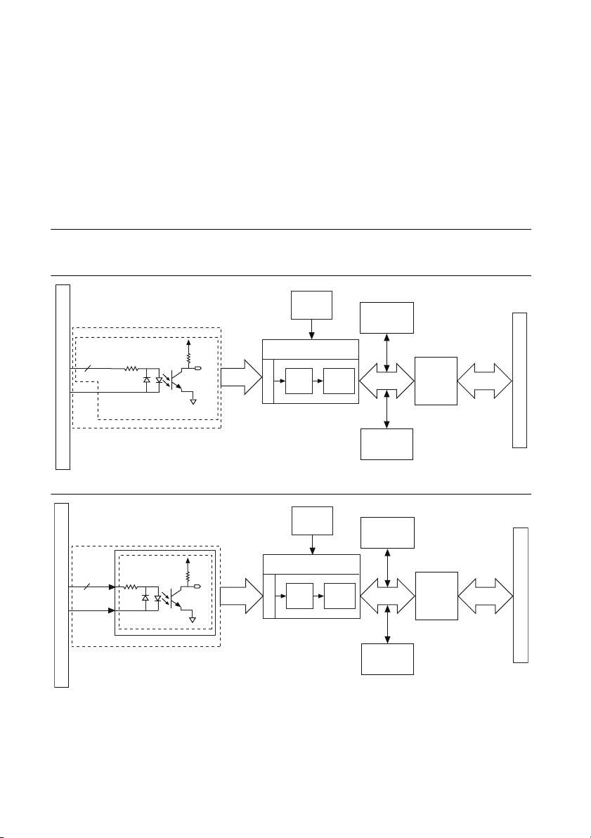
The following block diagrams illustrate the key functional components of the NI 651x devices.
Figure 1-1. NI 6510 Block Diagram
10 MHz
PX.<0..7>
32
COM
I/O Connector
x32 Bank Isolated Input Channels
VCC
DI
32 Digital
Inputs
Clock
Industrial Digital
Input Control FPGA
Digital
Filtering
Input Lines
Change
Detection
Flash
Memory
Data/Control
Configuration
Control
PCI Bus
Interface
Data/Control
PCI Bus
PX.<0..7>
8
PX.COM
I/O Connector
x8 Bank Isolated Digital Input Ports
x8 Inputs per Port
1-2 | ni.com
Figure 1-2. NI 6511 Block Diagram
10 MHz
Clock
Vcc
DI
64 Digital
Inputs
Industrial Digital
Input Control FPGA
Digital
Filtering
Input Lines
Change
Detection
Data/Control
Configuration
Flash
Memory
Control
PCI Bus
Interface
Data/Control
PCI/PXI/CompactPCI Bus
Page 12
Industrial Digital
Output Control FPGA
Output Lines
Programmable
Power-Up States
Watchdog Timer
64 Digital
Outputs
PX.COM
PX.Vcc
PX.<0..7>
8
x8 Bank Isolated Digital Output Ports
PCI/PXI/CompactPCI Bus
10 MHz
Clock
Data/Control
PCI Bus
Interface
Data/Control
Flash
Memory
Configuration
Control
DO
x8 Outputs per Port
Vol tage
Regulator
I/O Connector
Vol tage
Regulator
PX.COM (Vcc)
PX.<0..7>
I/O Connector
PX.GND
x8 Bank Isolated Digital Output Ports
x8 Outputs per Port
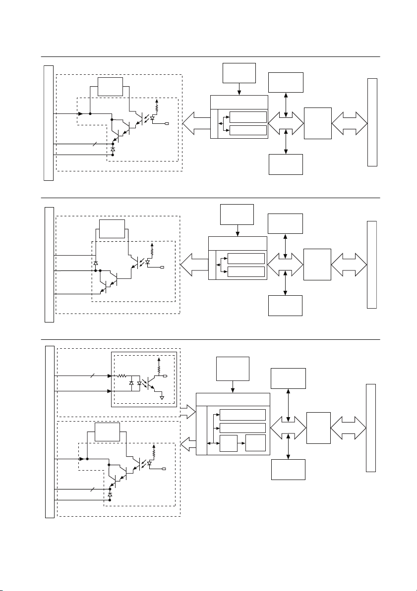
Figure 1-3. NI 6512 Block Diagram
Figure 1-4. NI 6513 Block Diagram
10 MHz
Clock
Industrial Digital
Output Control FPGA
Programmable
Output Lines
Power-Up States
Watchdog Timer
Configuration
64 Digital
DO
Outputs
Flash
Memory
Data/Control
Control
NI 651x User Manual
PCI Bus
Data/Control
Interface
PCI/PXI/CompactPCI Bus
PX.<0..7>
PX.COM
x4 Bank Isolated Digital Input Ports
I/O Connector
PX.Vcc
PX.<0..7>
PX.COM
x4 Bank Isolated Digital Output Ports
8
Vol tage
Regulator
8
Figure 1-5. NI 6514 Block Diagram
Vcc
DI
32
x8 Inputs per Port
x8 Outputs per Port
Digital
Inputs
Digital
Outputs
DO
DIO Lines
32
Industrial Digital
I/O Control FPGA
Filtering
10 MHz
Clock
Programmable
Power-Up States
Watchdog Timer
Digital
Change
Detection
Flash
Memory
Data/Control
Configuration
PCI Bus
Interface
Control
© National Instruments | 1-3
Data/Control
PCI/PXI/CompactPCI Bus
Page 13
Chapter 1 NI 651x Fundamentals
PX.COM (Vcc)
PX.<0..7>
PX.GND
DO
x8 Outputs per Port
x4 Bank Isolated Digital Output Ports
PCI/PXI/CompactPCI Bus
Data/Control
PCI Bus
Interface
10 MHz
Clock
32
Digital
Outputs
32
Digital
Inputs
I/O Connector
8
PX.COM
PX.<0..7>
Vcc
x4 Bank Isolated Digital Input Ports
x8 Inputs per Port
DI
Industrial Digital
I/O Control FPGA
DIO Lines
Programmable
Power-Up States
Watchdog Timer
Change
Detection
Digital
Filtering
Data/Control
Flash
Memory
Configuration
Control
Vol tage
Regulator
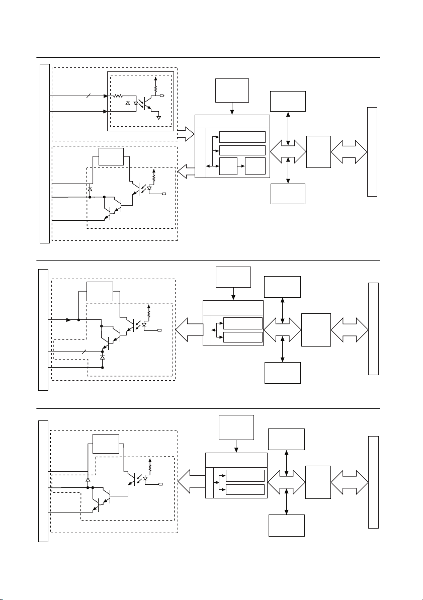
Figure 1-6. NI 6515 Block Diagram
Figure 1-7. NI 6516 Block Diagram
Vol tage
Regulator
VCC
I/O Connector
PX.<0..7>
32
COM.GND
x32 Bank Isolated Output Channels
10 MHz
Clock
Industrial Digital
Output Control FPGA
Programmable
Output Lines
Power-Up States
Watchdog Timer
32 Digital
DO
Outputs
Flash
Memory
Data/Control
Configuration
Control
PCI Bus
Interface
Data/Control
PCI Bus
COM (VCC)
PX.<0..7>
I/O Connector
GND
1-4 | ni.com
Figure 1-8. NI 6517 Block Diagram
Vol tage
Regulator
x32 Bank Isolated Output Channels
32 Digital
DO
Outputs
10 MHz
Clock
Industrial Digital
Output Control FPGA
Programmable
Power-Up States
Watchdog Timer
Output Lines
Flash
Memory
Data/Control
Configuration
Control
PCI Bus
Interface
Data/Control
PCI Bus
Page 14
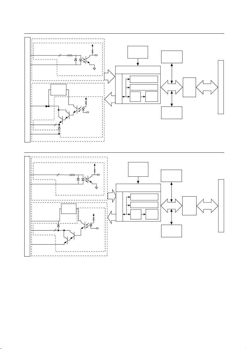
Figure 1-9. NI 6518 Block Diagram
I/O Connector
PCI Bus
Data/Control
PCI Bus
Interface
10 MHz
Clock
16
IN.COM
P<1..2>.<0..7>
VCC
x16 Bank Isolated Input Channels
DI
Industrial Digital
I/O Control FPGA
DIO Lines
Programmable
Power-Up States
Watchdog Timer
Change
Detection
Digital
Filtering
Data/Control
Flash
Memory
Configuration
Control
OUT.COM (VCC)
P<2..3>.<0..7>
GND
DO
Voltage
Regulator
x16 Bank Isolated Output Channels
16
16
Digital
Inputs
16
Digital
Outputs
NI 651x User Manual
P<0..1>.<0..7>
IN.COM
I/O Connector
VCC
P<2..3>.<0..7>
OUT.COM (GND)
16
x16 Bank Isolated
Input Channels
Vol tage
Regulator
16
x16 Bank Isolated
Output Channels
VCC
DI
16
Digital
Inputs
DO
16
Digital
Outputs
10 MHz
Industrial Digital
I/O Control FPGA
DIO Lines
Digital
Filtering
Clock
Programmable
Power-Up States
Watchdog Timer
Change
Detection
Figure 1-10. NI 6519 Block Diagram
Flash
Memory
Data/Control
Configuration
Control
PCI Bus
Interface
Data/Control
PCI Bus
© National Instruments | 1-5
Page 15
2
NI 651x Features
This chapter describes the National Instruments digital I/O features available for NI 651x
devices. For more information on the NI industrial DIO feature set, refer to the Complete
Industrial Digital I/O and Counter/Timer Tutorial. To access this tutorial, visit
and enter the code rdcidi.
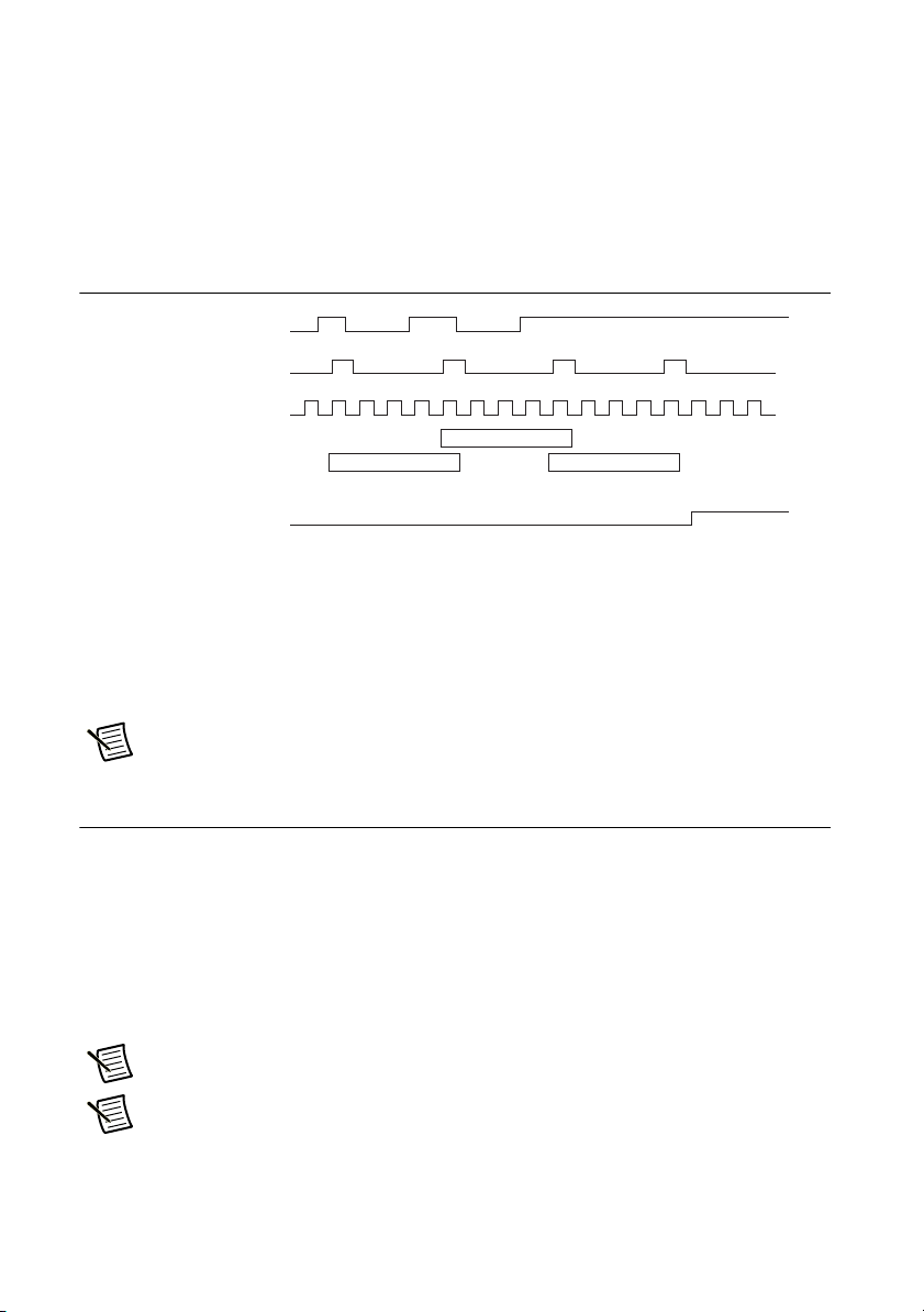
Digital Filtering
Use the digital filter option available on the NI 651x input lines to eliminate glitches on input
data. When used with change detection, filtering can also reduce the number of changes to
examine and process.
You can configure the digital input channels to pass through a digital filter after the
photocouplers, and you can control the timing interval the filter uses. The filter blocks pulses
that are shorter than half of the specified timing interval and passes pulses that are longer than
the specified interval. Intermediate-length pulses—pulses longer than half of the interval but less
than the interval—may or may not pass the filter.
The filter operates on the inputs from the photocouplers. Photocouplers turn on faster than they
turn off and pass rising edges faster than falling edges.
Table 2-1 lists the pulse widths guaranteed to be passed and blocked.
ni.com/info
Table 2-1. NI 651x Digital Filter Timing Intervals
Filter
Interval
t
interval
You can enable filtering on as many input lines as is necessary for your application. All filtered
lines share the same timing interval, which ranges from 200 s to 200 ms.
Internally, the filter uses two clocks: the sample clock and the filter clock. The sample clock has
a 100 ns period. The filter clock is generated by a counter and has a period equal to one half of
the specified timing interval. The input signal is sampled on each rising edge of the sample clock,
which is every 100 ns. However, a change in the input signal is recognized only if it maintains
its new state for at least two consecutive rising edges of the filter clock.
Pulse Width Passed Pulse Width Blocked
Low Pulse High Pulse Low Pulse High Pulse
t
+ 200 s t
interval
interval
t
/2 (t
interval
© National Instruments | 2-1
interval
/2) – 200
s
Page 16
Chapter 2 NI 651x Features
External
Signal
External
Signal
Sampled
Filter
Clock
Sample Clock (100 ns)
Filtered
Signal
HHHHH
HLLHH
HLLHH
A
B
C
The filter clock is programmable and allows you to control how long a pulse must last to be
recognized. The sample clock provides a fast sample rate to ensure that input pulses remain
constant between filter clocks.
Digital Filtering Example
Figure 2-1 shows a filter configuration with a t
Figure 2-1. Digital Filtering Example
In periods A and B, the filter blocks the glitches because the external signal does not remain
steadily high from one rising edge of the filter clock to the next. In period C, the filter passes the
transition because the external signal remains steadily high. Depending on when the transition
occurs, the filter may require up to two filter clocks—one full filter interval—to pass a transition.
Figure 2-1 shows a rising (0 to 1) transition. The same filtering applies to falling (1 to 0)
transitions.
filter interval (t
interval
/2 filter clock).
interval
Programmable Power-Up States
At power-up, the output drives on the NI 651x device is disabled. All output lines are
user-configurable for an on or off state. User-configurable power-up states are useful for
ensuring that the NI 651x device powers up in a known state.
To use MAX (recommended) to program the power-up states, select the device and click the
Properties button. Refer to the software documentation for information about how to program
the power-up states using NI-DAQ with LabVIEW or other National Instruments application
development environments (ADEs).
2-2 | ni.com
Note NI 6512/6513/6516/6517 devices do not support digital filtering.
Note The response time of programmable power-up states is 400 ms.
Note NI 6510/6511 devices do not support programmable power-up states.
Page 17
NI 651x User Manual
Change Detection
You can program NI 651x devices to send an interrupt when a change occurs on any input line.
The DIO device can monitor changes on selected input lines or on all input lines. It can monitor
for rising edges (0 to 1), falling edges (1 to 0), or both. When an input change occurs, the DIO
device generates an interrupt, and the NI-DAQ driver then notifies the software.
Note Excessive change detections can affect system performance. Use digital
filtering to minimize the effects of noisy input lines.
The DIO device sends a change detection when any one of the changes occurs, but it does not
report which line changed or if the line was rising or falling. After a change, you can read the
input lines to determine the current line states. The maximum rate of change detection is
determined by the software response time, which varies from system to system.
An overflow bit indicates that an additional rising or falling edge has been detected before the
software could process the previous change.
Refer to the software documentation for information about how to set up and implement the
change detection.
Change Detection Example
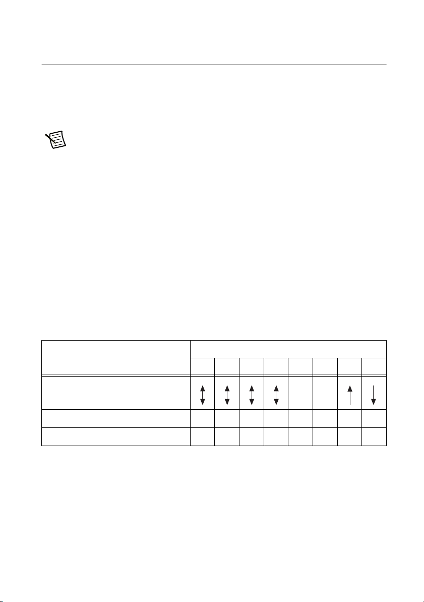
Table 2-2 shows a change detection example for six bits of one port.
Table 2-2. Change Detection Example
Bit
7 6 5 4 3 2 1 0
Changes to detect — —
Enable rising-edge detection yes yes yes yes no no yes no
Enable falling-edge detection yes yes yes yes no no no yes
This example assumes the following line connections:
• Bits 7, 6, 5, and 4 are connected to data lines from a four-bit TTL output device. The DIO
device detects any change in the input data so you can read the new data value.
• Bit 1 is connected to a limit sensor. The DIO device detects rising edges on the sensor,
which correspond to over-limit conditions.
• Bit 0 is connected to a switch. The software can react to any switch closure, which is
represented by a falling edge. If the switch closure is noisy, enable digital filtering for this
line.
© National Instruments | 2-3
Page 18

Chapter 2 NI 651x Features
In this example, the DIO device reports rising edges only on bit 1, falling edges only on bit 0,
and rising and falling edges on bits 7, 6, 5, and 4. The DIO device reports no changes for bits 3
and 2. After receiving notification of a change, you can read the port to determine the current
values of all eight lines. You cannot read the state of any lines that are configured for change
detection until the change detection interrupt occurs.
Note NI 6512/6513/6516/6517 devices do not support change detection.
Watchdog Timer
The watchdog timer is a software configurable feature used to set critical outputs to safe states
in the event of a software failure, a system crash, or any other loss of communication between
the application and the NI 651x device.
Note The NI-DAQmx Watchdog feature is meant to protect a system from software
errors and hangs. In the case of a PXI system with remote control through MXI, a lost
MXI connection could result in unexpected Watchdog behavior and therefore
improperly implemented Watchdog states.
When the watchdog timer is enabled, if the NI 651x device does not receive a watchdog reset
software command within the time specified for the watchdog timer, the outputs go to a
user-defined safe state and remain in that state until the watchdog timer is disarmed by the
application and new values are written, the NI 651x device is reset, or the computer is restarted.
The expiration signal that indicates an expired watchdog will continue to assert until the
watchdog is disarmed. After the watchdog timer expires, the NI 651x device ignores any writes
until the watchdog timer is disarmed.
You can set the watchdog timer timeout period to specify the amount of time that must elapse
before the watchdog timer expires. The counter on the watchdog timer is configurable up to
32
–1) 100 ns (approximately seven minutes) before it expires.
(2
Note NI 6510/6511 devices do not support the watchdog timer.
2-4 | ni.com
Page 19
3
Digital I/O
I/O Connector
NI 6510 I/O Connector
The 37-pin D-SUB connector on the NI 6510 provides access to the digital inputs. The digital
I/O available on this connector includes 32 inputs. For easy connection to the digital I/O
connector, use the National Instruments SH37F-37M shielded digital I/O cable with the CB-37F
connector block. For more information on digital I/O connectivity options, refer to Chapter 5,
Cables and Accessories.
Caution Do not make connections to the digital I/O that exceed the maximum I/O
specifications. Doing so could permanently damage the NI 6510 and the computer.
Refer to the NI 651x Specifications, available at
about maximum input ratings.
The input lines on the NI 6510 consist of input photocouplers, which react to a voltage
differential rather than only to a voltage increase. If the voltage connected to a digital input is
either greater than or less than the voltage connected to COM by at least the logic threshold, the
reading on the digital line will be logic high, even though in one instance the digital line has a
lower voltage level than COM.
ni.com/manuals, for information
For more information, refer to the Pin Assignments section.
NI 6511 I/O Connector
The 100-pin high-density SCSI connector on the NI 6511 provides access to the digital inputs.
The digital I/O available on this connector includes 64 inputs. For easy connection to the digital
I/O connector, use the National Instruments SH100-100-F shielded digital I/O cable with the
SCB-100 connector block, or use the R1005050 ribbon cable with the CB-50 or CB-50LP
connector block. For more information on digital I/O connectivity options, refer to Chapter 5,
Cables and Accessories.
Caution Do not make connections to the digital I/O that exceed the maximum I/O
specifications. Doing so could permanently damage the NI 6511 and the computer.
Refer to the NI 651x Specifications, available at
about maximum input ratings.
ni.com/manuals, for information
© National Instruments | 3-1
Page 20

Chapter 3 Digital I/O
The input lines on the NI 6511 consist of input photocouplers, which react to a voltage
differential rather than only to a voltage increase. If the voltage connected to a digital input is
either greater than or less than the voltage connected to PX.COM by at least the logic threshold,
the reading on the digital line will be logic high, even though in one instance the digital line has
a lower voltage level than PX.COM.
For more information, refer to the Pin Assignments section.
NI 6512/6513 I/O Connector
The 100-pin high-density SCSI connector on the NI 6512/6513 provides access to the digital
inputs and outputs. The digital I/O available on this connector includes 64 outputs. For easy
connection to the digital I/O connector, use the National Instruments SH100-100-F shielded
digital I/O cable with the SCB-100 connector block, or use the R1005050 ribbon cable with the
CB-50 or CB-50LP connector block. For more information on digital I/O connectivity options,
refer to Chapter 5, Cables and Accessories.
Caution Do not make connections to the digital I/O that exceed the maximum I/O
specifications. Doing so could permanently damage the NI 6512/6513 and the
computer. Refer to the NI 651x Specifications, available at
information about maximum input ratings.
The output lines on the NI 6512 consist of photocouplers and Darlington arrays. To connect to
these signals, connect a 5 V to 30 V power supply to VCC, connect COM (GND) to ground, and
cross a load between digital output and COM (GND).
ni.com/manuals, for
The output lines on the NI 6513 consist of photocouplers and Darlington arrays. To connect to
these signals, connect a 5 V to 30 V power supply to COM (VCC), connect GND to ground, and
cross a load between digital output and COM (VCC).
For more information, refer to the Pin Assignments section.
NI 6514/6515 I/O Connector
The 100-pin high-density SCSI connector on the NI 6514/6515 provides access to the digital
inputs and outputs. The digital I/O available on this connector includes 32 inputs and 32 outputs.
For easy connection to the digital I/O connector, use the National Instruments SH100-100-F
shielded digital I/O cable with the SCB-100 connector block, or use the R1005050 ribbon cable
with the CB-50 or CB-50LP connector block. For more information on digital I/O connectivity
options, refer to Chapter 5, Cables and Accessories.
Caution Do not make connections to the digital I/O that exceed the maximum I/O
specifications. Doing so could permanently damage the NI 6514/6515 and the
computer. Refer to the NI 651x Specifications, available at
information about maximum input ratings.
3-2 | ni.com
ni.com/manuals, for
Page 21

NI 651x User Manual
The input lines on the NI 6514/6515 consist of input photocouplers, which react to a voltage
differential rather than only to a voltage increase. If the voltage connected to a digital input is
either greater than or less than the voltage connected to PX.COM by at least the logic threshold,
the reading on the digital line will be logic high, even though in one instance the digital line has
a lower voltage level than PX.COM.
The output lines on the NI 6514 consist of photocouplers and Darlington arrays. To connect to
these signals, connect a 5 V to 30 V power supply to VCC, connect COM (GND) to ground, and
cross a load between digital output and COM (GND).
The output lines on the NI 6515 consist of photocouplers and Darlington arrays. To connect to
these signals, connect a 5 V to 30 V power supply to COM (VCC), connect GND to ground, and
cross a load between digital output and COM (VCC).
For more information, refer to the Pin Assignments section.
NI 6516/6517 I/O Connector
The 37-pin D-SUB connector on the NI 6516/6517 provides access to the digital inputs and
outputs. The digital I/O available on this connector includes 32 outputs. For easy connection to
the digital I/O connector, use the National Instruments SH37F-37M shielded digital I/O cable
with the CB-37F connector block. For more information on digital I/O connectivity options,
refer to Chapter 5, Cables and Accessories.
Caution Do not make connections to the digital I/O that exceed the maximum I/O
specifications. Doing so could permanently damage the NI 6516/6517 and the
computer. Refer to the NI 651x Specifications, available at ni.com/manuals, for
information about maximum input ratings.
The output lines on the NI 6516 consist of photocouplers and Darlington arrays. To connect to
these signals, connect a 5 V to 30 V power supply to VCC, connect COM (GND) to ground, and
cross a load between digital output and COM (GND).
The output lines on the NI 6517 consist of photocouplers and Darlington arrays. To connect to
these signals, connect a 5 V to 30 V power supply to COM (VCC), connect GND to ground, and
cross a load between digital output and COM (VCC).
For more information, refer to the Pin Assignments section.
NI 6518/6519 I/O Connector
The 37-pin D-SUB connector on the NI 6518/6519 provides access to the digital inputs and
outputs. The digital I/O available on this connector includes 32 inputs and 32 outputs. For easy
connection to the digital I/O connector, use the National Instruments SH37F-37M shielded
digital I/O cable with the CB-37F connector block. For more information on digital I/O
connectivity options, refer to Chapter 5, Cables and Accessories.
© National Instruments | 3-3
Page 22

Chapter 3 Digital I/O
Caution Do not make connections to the digital I/O that exceed the maximum I/O
specifications. Doing so could permanently damage the NI 6518/6519 and the
computer. Refer to the NI 651x Specifications, available at
ni.com/manuals, for
information about maximum input ratings.
The input lines on the NI 6518/6519 consist of input photocouplers, which react to a voltage
differential rather than only to a voltage increase. If the voltage connected to a digital input is
either greater than or less than the voltage connected to IN.COM by at least the logic threshold,
the reading on the digital line will be logic high, even though in one instance the digital line has
a lower voltage level than IN.COM.
The output lines on the NI 6518 consist of photocouplers and Darlington arrays. To connect to
these signals, connect a 5 V to 30 V power supply to VCC, connect OUT.COM (GND) to
ground, and cross a load between digital output and OUT.COM (GND).
The output lines on the NI 6519 consist of photocouplers and Darlington arrays. To connect to
these signals, connect a 5 V to 30 V power supply to OUT.COM (VCC), connect GND to
ground, and cross a load between digital output and OUT.COM (VCC).
For more information, refer to the Pin Assignments section.
3-4 | ni.com
Page 23

NI 651x User Manual
Pin Assignments
NI 6510 Pin Assignments
Figure 3-1 shows the pin assignments for the SH37F-37M cable when connecting to the NI 6510
device. The naming convention for each pin is PX.Y, where X is the port (P) number, and Y is the
line number or name.
Figure 3-1. NI 6510 Pin Assignments
1
P0.1
P0.3
P0.5
P0.7
P1.0
P1.2
P1.4
P1.6
COM
P2.1
P2.3
P2.5
P2.7
P3.0
P3.2
P3.4
P3.6
COM
20
21
22
23
24
25
26
27
28
29
30
31
32
33
34
35
36
37
P0.0
2
P0.2
3
P0.4
4
P0.6
5
COM
6
P1.1
7
P1.3
8
P1.5
9
P1.7
P2.0
10
P2.2
11
P2.4
12
P2.6
13
COM
14
P3.1
15
P3.3
16
P3.5
17
P3.7
18
COM
19
For more information on the NI 6510 signals, refer to the Signal Descriptions section.
© National Instruments | 3-5
Page 24

Chapter 3 Digital I/O
NI 6511 SH100-100-F Pin Assignments
Figure 3-2 shows the pin assignments for the SH100-100-F cable when connecting to the
NI 6511 device. The naming convention for each pin is PX.Y, where X is the port (P) number,
and Y is the line number or name.
3-6 | ni.com
Page 25

NI 651x User Manual
25
24
23
22
21
20
19
18
17
16
15
14
13
12
11
10
9
8
7
6
5
4
3
2
1
75
74
73
72
71
70
69
68
67
66
65
64
63
62
61
60
59
58
57
56
55
54
53
52
51
50
49
48
47
46
45
44
43
42
41
40
39
38
37
36
35
34
33
32
31
30
29
28
27
26
100
99
98
97
96
95
94
93
92
91
90
89
88
87
86
85
84
83
82
81
80
79
78
77
76
NC
P6.COM
P6.COM
P6.COM
P6.COM
P6.7
P6.6
P6.5
P6.4
P6.3
P6.2
P6.1
P6.0
P4.COM
P4.COM
P4.COM
P4.COM
P4.7
P4.6
P4.5
P4.4
P4.3
P4.2
P4.1
P4.0
NC
P2.COM
P2.COM
P2.COM
P2.COM
P2.7
P2.6
P2.5
P2.4
P2.3
P2.2
P2.1
P2.0
P0.COM
P0.COM
P0.COM
P0.COM
P0.7
P0.6
P0.5
P0.4
P0.3
P0.2
P0.1
P0.0
NC
P7.COM
P7.COM
P7.COM
P7.COM
P7.7
P7.6
P7.5
P7.4
P7.3
P7.2
P7.1
P7.0
P5.COM
P5.COM
P5.COM
P5.COM
P5.7
P5.6
P5.5
P5.4
P5.3
P5.2
P5.1
P5.0
NC
P3.COM
P3.COM
P3.COM
P3.COM
P3.7
P3.6
P3.5
P3.4
P3.3
P3.2
P3.1
P3.0
P1.COM
P1.COM
P1.COM
P1.COM
P1.7
P1.6
P1.5
P1.4
P1.3
P1.2
P1.1
P1.0
NC = No Connect
Figure 3-2. NI 6511 Pin Assignments for the SH100-100-F Cable
© National Instruments | 3-7
Page 26

Chapter 3 Digital I/O
For more information on the NI 6511 signals, refer to the Signal Descriptions section.
NI 6511 R1005050 Pin Assignments
Figure 3-3 shows the pin assignments for the R1005050 cable when connecting to the NI 6511
device. The naming convention for each pin is PX.Y, where X is the port (P) number, and Y is the
line number or name.
Figure 3-3. NI 6511 Pin Assignments for the R1005050 Cable
Positions 1 through 50
P0.0
P0.2
P0.4
P0.6
P0.COM
P0.COM
P2.0
P2.2
P2.4
P2.6
P2.COM
P2.COM
NC
P4.1
P4.3
P4.5
P4.7
P4.COM
P4.COM
P6.1
P6.3
P6.5
P6.7
P6.COM
P6.COM
12
3 4
56
78
910
11 12
13 14
15 16
17 18
19 20
21 22
23 24
25 26
27 28
29 30
31 32
33 34
35 36
37 38
3940
41 42
43 44
45 46
47 48
49 50
P0.1
P0.3
P0.5
P0.7
P0.COM
P0.COM
P2.1
P2.3
P2.5
P2.7
P2.COM
P2.COM
P4.0
P4.2
P4.4
P4.6
P4.COM
P4.COM
P6.0
P6.2
P6.4
P6.6
P6.COM
P6.COM
NC
NC = No Connect
Positions 51 through 100
P1.0
P1.2
P1.4
P1.6
P1.COM
P1.COM
P3.0
P3.2
P3.4
P3.6
P3.COM
P3.COM
NC
P5.1
P5.3
P5.5
P5.7
P5.COM
P5.COM
P7.1
P7.3
P7.5
P7.7
P7.COM
P7.COM
12
3 4
56
78
910
11 12
13 14
15 16
17 18
19 20
21 22
23 24
25 26
27 28
29 30
31 32
33 34
35 36
37 38
3940
41 42
43 44
45 46
47 48
49 50
P1.1
P1.3
P1.5
P1.7
P1.COM
P1.COM
P3.1
P3.3
P3.5
P3.7
P3.COM
P3.COM
P5.0
P5.2
P5.4
P5.6
P5.COM
P5.COM
P7.0
P7.2
P7.4
P7.6
P7.COM
P7.COM
NC
For more information on the NI 6511 signals, refer to the Signal Descriptions section.
NI 6512 SH100-100-F Pin Assignments
Figure 3-4 shows the pin assignments for the SH100-100-F cable when connecting to the
NI 6512 device. The naming convention for each pin is PX.Y, where X is the port (P) number,
and Y is the line number or name.
3-8 | ni.com
Page 27

NI 651x User Manual
25
24
23
22
21
20
19
18
17
16
15
14
13
12
11
10
9
8
7
6
5
4
3
2
1
75
74
73
72
71
70
69
68
67
66
65
64
63
62
61
60
59
58
57
56
55
54
53
52
51
50
49
48
47
46
45
44
43
42
41
40
39
38
37
36
35
34
33
32
31
30
29
28
27
26
100
99
98
97
96
95
94
93
92
91
90
89
88
87
86
85
84
83
82
81
80
79
78
77
76
P6.+5V
P6.VCC
P6.VCC
P6.VCC
P6.COM (P6.GND)
P6.7
P6.6
P6.5
P6.4
P6.3
P6.2
P6.1
P6.0
P4.VCC
P4.VCC
P4.VCC
P4.COM (P4.GND)
P4.7
P4.6
P4.5
P4.4
P4.3
P4.2
P4.1
P4.0
NC
P2.VCC
P2.VCC
P2.VCC
P2.COM (P2.GND)
P2.7
P2.6
P2.5
P2.4
P2.3
P2.2
P2.1
P2.0
P0.VCC
P0.VCC
P0.VCC
P0.COM (P0.GND)
P0.7
P0.6
P0.5
P0.4
P0.3
P0.2
P0.1
P0.0
P7.+5V
P7.VCC
P7.VCC
P7.VCC
P7.COM (P7.GND)
P7.7
P7.6
P7.5
P7.4
P7.3
P7.2
P7.1
P7.0
P5.VCC
P5.VCC
P5.VCC
P5.COM (P5.GND)
P5.7
P5.6
P5.5
P5.4
P5.3
P5.2
P5.1
P5.0
NC
P3.VCC
P3.VCC
P3.VCC
P3.COM (P3.GND)
P3.7
P3.6
P3.5
P3.4
P
3.3
P3.2
P3.1
P3.0
P1.VCC
P1.VCC
P1.VCC
P1.COM (P1.GND)
P1.7
P1.6
P1.5
P1.4
P1.3
P1.2
P1.1
P1.0
NC = No Connect
Figure 3-4. NI 6512 Pin Assignments for the SH100-100-F Cable
© National Instruments | 3-9
Page 28

Chapter 3 Digital I/O
For more information on the NI 6512 signals, refer to the Signal Descriptions section.
NI 6512 R1005050 Pin Assignments
Figure 3-5 shows the pin assignments for the R1005050 cable when connecting to the NI 6512
device. The naming convention for each pin is PX.Y, where X is the port (P) number, and Y is the
line number or name.
Figure 3-5. NI 6512 Pin Assignments for the R1005050 Cable
Positions 1 through 50 Positions 51 through 100
P0.0
P0.2
P0.4
P0.6
P0.COM (P0.GND)
P0.VCC
P2.0
P2.2
P2.4
P2.6
P2.COM (P2.GND)
P2.VCC
NC
P4.1
P4.3
P4.5
P4.7
P4.VCC
P4.VCC
P6.1
P6.3
P6.5
P6.7
P6.VCC
P6.VCC
12
3 4
56
78
910
11 12
13 14
15 16
17 18
19 20
21 22
23 24
25 26
27 28
29 30
31 32
33 34
35 36
37 38
3940
41 42
43 44
45 46
47 48
49 50
P0.1
P0.3
P0.5
P0.7
P0.VCC
P0.VCC
P2.1
P2.3
P2.5
P2.7
P2.VCC
P2.VCC
P4.0
P4.2
P4.4
P4.6
P4.COM (P4.GND)
P4.VCC
P6.0
P6.2
P6.4
P6.6
P6.COM (P6.GND)
P6.VCC
P6.+5V
NC = No Connect
P1.0
P1.2
P1.4
P1.6
P1.COM (P1.GND)
P1.VCC
P3.0
P3.2
P3.4
P3.6
P3.COM (P3.GND)
P3.VCC
NC
P5.1
P5.3
P5.5
P5.7
P5.VCC
P5.VCC
P7.1
P7.3
P7.5
P7.7
P7.VCC
P7.VCC
12
3 4
56
78
910
11 12
13 14
15 16
17 18
19 20
21 22
23 24
25 26
27 28
29 30
31 32
33 34
35 36
37 38
3940
41 42
43 44
45 46
47 48
49 50
P1.1
P1.3
P1.5
P1.7
P1.VCC
P1.VCC
P3.1
P3.3
P3.5
P3.7
P3.VCC
P3.VCC
P5.0
P5.2
P5.4
P5.6
P5.COM (P5.GND)
P5.VCC
P7.0
P7.2
P7.4
P7.6
P7.COM (P7.GND)
P7.VCC
P7.+5V
For more information on the NI 6512 signals, refer to the Signal Descriptions section.
NI 6513 SH100-100-F Pin Assignments
Figure 3-6 shows the pin assignments for the SH100-100-F cable when connecting to the
NI 6513 device. The naming convention for each pin is PX.Y, where X is the port (P) number,
and Y is the line number or name.
3-10 | ni.com
Page 29

NI 651x User Manual
25
24
23
22
21
20
19
18
17
16
15
14
13
12
11
10
9
8
7
6
5
4
3
2
1
75
74
73
72
71
70
69
68
67
66
65
64
63
62
61
60
59
58
57
56
55
54
53
52
51
50
49
48
47
46
45
44
43
42
41
40
39
38
37
36
35
34
33
32
31
30
29
28
27
26
100
99
98
97
96
95
94
93
92
91
90
89
88
87
86
85
84
83
82
81
80
79
78
77
76
P6.+5V
P6.GND
P6.GND
P6.GND
P6.COM (P6.VCC)
P6.7
P6.6
P6.5
P6.4
P6.3
P6.2
P6.1
P6.0
P4.GND
P4.GND
P4.GND
P4.COM (P4.VCC)
P4.7
P4.6
P4.5
P4.4
P4.3
P4.2
P4.1
P4.0
NC
P2.GND
P2.GND
P2.GND
P2.COM (P2.VCC)
P2.7
P2.6
P2.5
P2.4
P2.3
P2.2
P2.1
P2.0
P0.GND
P0.GND
P0.GND
P0.COM (P0.VCC)
P0.7
P0.6
P0.5
P0.4
P0.3
P0.2
P0.1
P0.0
P7.+5V
P7.GND
P7.GND
P7.GND
P7.COM (P7.VCC)
P7.7
P7.6
P7.5
P7.4
P7.3
P7.2
P7.1
P7.0
P5.GND
P5.GND
P5.GND
P5.COM (P5.VCC)
P5.7
P5.6
P5.5
P5.4
P5.3
P5.2
P5.1
P5.0
NC
P3.GND
P3.GND
P3.GND
P3.COM (P3.VCC)
P3.7
P3.6
P3.5
P3.4
P
3.3
P3.2
P3.1
P3.0
P1.GND
P1.GND
P1.GND
P1.COM (P1.VCC)
P1.7
P1.6
P1.5
P1.4
P1.3
P1.2
P1.1
P1.0
NC = No Connect
Figure 3-6. NI 6513 Pin Assignments for the SH100-100-F Cable
© National Instruments | 3-11
Page 30

Chapter 3 Digital I/O
For more information on the NI 6513 signals, refer to the Signal Descriptions section.
NI 6513 R1005050 Pin Assignments
Figure 3-7 shows the pin assignments for the R1005050 cable when connecting to the NI 6513
device. The naming convention for each pin is PX.Y, where X is the port (P) number, and Y is the
line number or name.
Figure 3-7. NI 6513 Pin Assignments for the R1005050 Cable
Positions 1 through 50 Positions 51 through 100
P0.0
P0.2
P0.4
P0.6
P0.COM (P0.VCC)
P0.GND
P2.0
P2.2
P2.4
P2.6
P2.COM (P2.VCC)
P2.GND
NC
P4.1
P4.3
P4.5
P4.7
P4.GND
P4.GND
P6.1
P6.3
P6.5
P6.7
P6.GND
P6.GND
12
3 4
56
78
910
11 12
13 14
15 16
17 18
19 20
21 22
23 24
25 26
27 28
29 30
31 32
33 34
35 36
37 38
3940
41 42
43 44
45 46
47 48
49 50
P0.1
P0.3
P0.5
P0.7
P0.GND
P0.GND
P2.1
P2.3
P2.5
P2.7
P2.GND
P2.GND
P4.0
P4.2
P4.4
P4.6
P4.COM (P4.VCC)
P4.GND
P6.0
P6.2
P6.4
P6.6
P6.COM (P6.VCC)
P6.GND
P6.+5V
NC = No Connect
P1.0
P1.2
P1.4
P1.6
P1.COM (P1.VCC)
P1.GND
P3.0
P3.2
P3.4
P3.6
P3.COM (P3.VCC)
P3.GND
NC
P5.1
P5.3
P5.5
P5.7
P5.GND
P5.GND
P7.1
P7.3
P7.5
P7.7
P7.GND
P7.GND
12
3 4
56
78
910
11 12
13 14
15 16
17 18
19 20
21 22
23 24
25 26
27 28
29 30
31 32
33 34
35 36
37 38
3940
41 42
43 44
45 46
47 48
49 50
P1.1
P1.3
P1.5
P1.7
P1.GND
P1.GND
P3.1
P3.3
P3.5
P3.7
P3.GND
P3.GND
P5.0
P5.2
P5.4
P5.6
P5.COM (P5.VCC)
P5.GND
P7.0
P7.2
P7.4
P7.6
P7.COM (P7.VCC)
P7.GND
P7.+5V
For more information on the NI 6513 signals, refer to the Signal Descriptions section.
NI 6514 SH100-100-F Pin Assignments
Figure 3-8 shows the pin assignments for the SH100-100-F cable when connecting to the
NI 6514 device. The naming convention for each pin is PX.Y, where X is the port (P) number,
and Y is the line number or name.
3-12 | ni.com
Page 31

NI 651x User Manual
Figure 3-8. NI 6514 Pin Assignments for the SH100-100-F Cable
1
51
P0.0
P0.1
P0.2
P0.3
P0.4
P0.5
P0.6
P0.7
P0.COM
P0.COM
P0.COM
P0.COM
P2.0
P2.1
P2.2
P2.3
P2.4
P2.5
P2.6
P2.7
P2.COM
P2.COM
P2.COM
P2.COM
NC
P4.0
P4.1
P4.2
P4.3
P4.4
P4.5
P4.6
P4.7
P4.COM (P4.GND)
P4.VCC
P4.VCC
P4.VCC
P6.0
P6.1
P6.2
P6.3
P6.4
P6.5
P6.6
P6.7
P6.COM (P6.GND)
P6.VCC
P6.VCC
P6.VCC
P6.+5V
10
11
12
13
14
15
16
17
18
19
20
21
22
23
24
25
26
27
28
29
30
31
32
33
34
35
36
37
38
39
40
41
42
43
44
45
46
47
48
49
50
2
52
3
53
4
54
5
55
6
56
57
7
58
8
59
9
60
61
62
63
64
65
66
67
68
69
70
71
72
73
74
75
76
77
78
79
80
81
82
83
84
85
86
87
88
89
90
91
92
93
94
95
96
97
98
99
100
P1.0
P1.1
P1.2
P1.3
P1.4
P1.5
P1.6
P1.7
P1.COM
P1.COM
P1.COM
P1.COM
P3.0
P3.1
P3.2
P3.3
P3.4
P3.5
P3.6
P3.7
P3.COM
P3.COM
P3.COM
P3.COM
NC
P5.0
P5.1
P5.2
P5.3
P5.4
P5.5
P5.6
P5.7
P5.COM (P5.GND)
P5.VCC
P5.VCC
P5.VCC
P7.0
P7.1
P7.2
P7.3
P7.4
P7.5
P7.6
P7.7
P7.COM (P7.GND)
P7.VCC
P7.VCC
P7.VCC
P7.+5V
NC = No Connect
© National Instruments | 3-13
Page 32

Chapter 3 Digital I/O
P6.VCC
P6.VCC
P6.7
P6.5
P6.3
P6.1
P4.VCC
P4.VCC
P4.7
P4.5
P4.3
P4.1
NC
P2.COM
P2.COM
P2.6
P2.4
P2.2
P2.0
P0.COM
P0.COM
P0.6
P0.4
P0.2
P0.0
P6.+5V
P6.COM (P6.GND)
P6.6
P6.2
P6.0
P4.VCC
P4.COM (P4.GND)
P6.VCC
P6.4
P4.6
P4.4
P4.2
P4.0
P2.COM
P2.COM
P2.7
P2.5
P2.3
P2.1
P0.COM
P0.COM
P0.7
P0.5
P0.3
P0.1
49 50
47 48
45 46
43 44
41 42
3940
37 38
35 36
33 34
31 32
29 30
27 28
25 26
23 24
21 22
19 20
17 18
15 16
13 14
11 12
910
78
56
3 4
12
Positions 1 through 50 Positions 51 through 100
49 50
47 48
45 46
43 44
41 42
3940
37 38
35 36
33 34
31 32
29 30
27 28
25 26
23 24
21 22
19 20
17 18
15 16
13 14
11 12
910
78
56
3 4
12
P7.VCC
P7.VCC
P7.7
P7.5
P7.3
P7.1
P5.VCC
P5.VCC
P5.7
P5.5
P5.3
P5.1
NC
P3.COM
P3.COM
P3.6
P3.4
P3.2
P3.0
P1.COM
P1.COM
P1.6
P1.4
P1.2
P1.0
P7.+5V
P7.COM (P7.GND)
P7.6
P7.2
P7.0
P5.VCC
P5.COM (P5.GND)
P7.VCC
P7.4
P5.6
P5.4
P5.2
P5.0
P3.COM
P3.COM
P3.7
P3.5
P3.3
P3.1
P1.COM
P1.COM
P1.7
P1.5
P1.3
P1.1
NC = No Connect
For more information on the NI 6514 signals, refer to the Signal Descriptions section.
NI 6514 R1005050 Pin Assignments
Figure 3-9 shows the pin assignments for the R1005050 cable when connecting to the NI 6514
device. The naming convention for each pin is PX.Y, where X is the port (P) number, and Y is the
line number or name.
Figure 3-9. NI 6514 Pin Assignments for the R1005050 Cable
For more information on the NI 6514 signals, refer to the Signal Descriptions section.
NI 6515 SH100-100-F Pin Assignments
Figure 3-10 shows the pin assignments for the SH100-100-F cable when connecting to the
NI 6515 device. The naming convention for each pin is PX.Y, where X is the port (P) number,
and Y is the line number or name.
3-14 | ni.com
Page 33

NI 651x User Manual
Figure 3-10. NI 6515 Pin Assignments for the SH100-100-F Cable
1
P0.0
P0.1
P0.2
P0.3
P0.4
P0.5
P0.6
P0.7
P0.COM
P0.COM
P0.COM
P0.COM
P2.0
P2.1
P2.2
P2.3
P2.4
P2.5
P2.6
P2.7
P2.COM
P2.COM
P2.COM
P2.COM
NC
P4.0
P4.1
P4.2
P4.3
P4.4
P4.5
P4.6
P4.7
P4.COM (P4.VCC)
P4.GND
P4.GND
P4.GND
P6.0
P6.1
P6.2
P6.3
P6.4
P6.5
P6.6
P6.7
P6.COM (P6.VCC)
P6.GND
P6.GND
P6.GND
P6.+5V
51
52
53
54
55
56
57
58
59
60
61
62
63
64
65
66
67
68
69
70
71
72
73
74
75
76
77
78
79
80
81
82
83
84
85
86
87
88
89
90
91
92
93
94
95
96
97
98
99
100
P1.0
P1.1
P1.2
P1.3
P1.4
P1.5
P1.6
P1.7
P1.COM
P1.COM
P1.COM
P1.COM
P3.0
P3.1
P3.2
P3.3
P3.4
P3.5
P3.6
P3.7
P3.COM
P3.COM
P3.COM
P3.COM
NC
P5.0
P5.1
P5.2
P5.3
P5.4
P5.5
P5.6
P5.7
P5.COM (P5.VCC)
P5.GND
P5.GND
P5.GND
P7.0
P7.1
P7.2
P7.3
P7.4
P7.5
P7.6
P7.7
P7.COM (P7.VCC)
P7.GND
P7.GND
P7.GND
P7.+5V
2
3
4
5
6
7
8
9
10
11
12
13
14
15
16
17
18
19
20
21
22
23
24
25
26
27
28
29
30
31
32
33
34
35
36
37
38
39
40
41
42
43
44
45
46
47
48
49
50
NC = No Connect
© National Instruments | 3-15
Page 34

Chapter 3 Digital I/O
P6.GND
P6.GND
P6.7
P6.5
P6.3
P6.1
P4.GND
P4.GND
P4.7
P4.5
P4.3
P4.1
NC
P2.COM
P2.COM
P2.6
P2.4
P2.2
P2.0
P0.COM
P0.COM
P0.6
P0.4
P0.2
P0.0
P6.+5V
P6.COM (P6.VCC)
P6.6
P6.2
P6.0
P4.GND
P4.COM (P4.VCC)
P6.GND
P6.4
P4.6
P4.4
P4.2
P4.0
P2.COM
P2.COM
P2.7
P2.5
P2.3
P2.1
P0.COM
P0.COM
P0.7
P0.5
P0.3
P0.1
49 50
47 48
45 46
43 44
41 42
3940
37 38
35 36
33 34
31 32
29 30
27 28
25 26
23 24
21 22
19 20
17 18
15 16
13 14
11 12
910
78
56
3 4
12
Positions 1 through 50 Positions 51 through 100
49 50
47 48
45 46
43 44
41 42
3940
37 38
35 36
33 34
31 32
29 30
27 28
25 26
23 24
21 22
19 20
17 18
15 16
13 14
11 12
910
78
56
3 4
12
P7.GND
P7.GND
P7.7
P7.5
P7.3
P7.1
P5.GND
P5.GND
P5.7
P5.5
P5.3
P5.1
NC
P3.COM
P3.COM
P3.6
P3.4
P3.2
P3.0
P1.COM
P1.COM
P1.6
P1.4
P1.2
P1.0
P7.+5V
P7.COM (P7.VCC)
P7.6
P7.2
P7.0
P5.GND
P5.COM (P5.VCC)
P7.GND
P7.4
P5.6
P5.4
P5.2
P5.0
P3.COM
P3.COM
P3.7
P3.5
P3.3
P3.1
P1.COM
P1.COM
P1.7
P1.5
P1.3
P1.1
NC = No Connect
For more information on the NI 6515 signals, refer to the Signal Descriptions section.
NI 6515 R1005050 Pin Assignments
Figure 3-11 shows the pin assignments for the R1005050 cable when connecting to the NI 6515
device. The naming convention for each pin is PX.Y, where X is the port (P) number, and Y is the
line number or name.
Figure 3-11. NI 6515 Pin Assignments for the R1005050 Cable
For more information on the NI 6515 signals, refer to the Signal Descriptions section.
3-16 | ni.com
Page 35

NI 651x User Manual
1
2
3
4
5
6
7
8
9
10
11
12
13
14
15
16
17
18
19
20
21
22
23
24
25
26
27
28
29
30
31
32
33
34
35
36
37
P0.0
P0.2
P0.4
P0.6
VCC
P1.1
P1.3
P1.5
P1.7
P2.0
P2.2
P2.4
P2.6
VCC
P3.1
P3.3
P3.5
P3.7
COM (GND)
P0.1
P0.3
P0.5
P0.7
P1.0
P1.2
P1.4
P1.6
VCC
P2.1
P2.3
P2.5
P2.7
P3.0
P3.2
P3.4
P3.6
VCC
NI 6516 Pin Assignments
Figure 3-12 shows the pin assignments for the SH37F-37M cable when connecting to the
NI 6516 device. The naming convention for each pin is PX.Y, where X is the port (P) number,
and Y is the line number or name.
Figure 3-12. NI 6516 Pin Assignments
For more information on the NI 6516 signals, refer to the Signal Descriptions section.
© National Instruments | 3-17
Page 36

Chapter 3 Digital I/O
NI 6517 Pin Assignments
Figure 3-13 shows the pin assignments for the SH37F-37M cable when connecting to the
NI 6517 device. The naming convention for each pin is PX.Y, where X is the port (P) number,
and Y is the line number or name.
Figure 3-13. NI 6517 Pin Assignments
1
P0.1
P0.3
P0.5
P0.7
P1.0
P1.2
P1.4
P1.6
GND
P2.1
P2.3
P2.5
P2.7
P3.0
P3.2
P3.4
P3.6
GND
20
21
22
23
24
25
26
27
28
29
30
31
32
33
34
35
36
37
2
3
4
5
6
7
8
9
10
11
12
13
14
15
16
17
18
19
P0.0
P0.2
P0.4
P0.6
GND
P1.1
P1.3
P1.5
P1.7
P2.0
P2.2
P2.4
P2.6
GND
P3.1
P3.3
P3.5
P3.7
COM (VCC)
For more information on the NI 6517 signals, refer to the Signal Descriptions section.
3-18 | ni.com
Page 37

NI 651x User Manual
NI 6518 Pin Assignments
Figure 3-14 shows the pin assignments for the SH37F-37M cable when connecting to the
NI 6518 device. The naming convention for each pin is PX.Y, where X is the port (P) number,
and Y is the line number or name.
Figure 3-14. NI 6518 Pin Assignments
1
P0.1
P0.3
P0.5
P0.7
P1.1
P1.3
P1.5
P1.7
VCC
VCC
P2.1
P2.3
P2.5
P2.7
P3.1
P3.3
P3.5
P3.7
20
21
22
23
24
25
26
27
28
29
30
31
32
33
34
35
36
37
P0.0
2
P0.2
3
P0.4
4
P0.6
5
P1.0
6
P1.2
7
P1.4
8
P1.6
9
IN.COM
VCC
10
P2.0
11
P2.2
12
P2.4
13
P2.6
14
P3.0
15
P3.2
16
P3.4
17
P3.6
18
OUT.COM (GND)
19
For more information on the NI 6518 signals, refer to the Signal Descriptions section.
© National Instruments | 3-19
Page 38

Chapter 3 Digital I/O
NI 6519 Pin Assignments
Figure 3-15 shows the pin assignments for the SH37F-37M cable when connecting to the
NI 6519 device. The naming convention for each pin is PX.Y, where X is the port (P) number,
and Y is the line number or name.
Figure 3-15. NI 6519 Pin Assignments
1
P0.1
P0.3
P0.5
P0.7
P1.1
P1.3
P1.5
P1.7
GND
GND
P2.1
P2.3
P2.5
P2.7
P3.1
P3.3
P3.5
P3.7
20
21
22
23
24
25
26
27
28
29
30
31
32
33
34
35
36
37
P0.0
2
P0.2
3
P0.4
4
P0.6
5
P1.0
6
P1.2
7
P1.4
8
P1.6
9
IN.COM
GND
10
P2.0
11
P2.2
12
P2.4
13
P2.6
14
P3.0
15
P3.2
16
P3.4
17
P3.6
18
OUT.COM (VCC)
19
For more information on the NI 6519 signals, refer to the Signal Descriptions section.
3-20 | ni.com
Page 39

NI 651x User Manual
Signal Descriptions
NI 6510 Signal Descriptions
Table 3-1. NI 6510 Signal Descriptions
Input or
Pin Number Signal Name
1, 2, 3, 4, 20, 21, 22, 23P0.<0..7> Input Data lines for port 0
5, 14, 19, 28, 37 COM Input Common lines for all ports
6, 7, 8, 9, 24, 25, 26, 27P1.<0..7> Input Data lines for port 1
10, 11, 12, 29, 30, 31, 32P2.<0..7> Input Data lines for port 2
Output
Signal Description
15, 16, 17, 18, 33, 34,
35, 36
P3.<0..7> Input Data lines for port 3
NI 6511 Signal Descriptions
Table 3-2. NI 6511 Signal Descriptions
Input or
Pin Number Signal Name
1, 2, 3, 4, 5, 6, 7, 8, 13, 14,
15, 16, 17, 18, 19, 20, 26, 27,
28, 29, 30, 31, 32, 33, 38, 39,
40, 41, 42, 43, 44, 45, 51, 52,
53, 54, 55, 56, 57, 58, 63, 64,
65, 66, 67, 68, 69, 70, 76, 77,
78, 79, 80, 81, 82, 83, 88, 89,
90, 91, 92, 93, 94, 95
9, 10, 11, 12, 21, 22, 23, 24,
34, 35, 36, 37, 46, 47, 48, 49,
59, 60, 61, 62, 71, 72, 73, 74,
84, 85, 86, 87, 96, 97, 98, 99
25, 50, 75, 100 NC — No connection
P<0..7>.<0..7> Input Data lines for ports
P<0..7>.COM Input Common lines for
Output
Signal Description
0 through 7
ports 0 through 7
© National Instruments | 3-21
Page 40

Chapter 3 Digital I/O
NI 6512 Signal Descriptions
Table 3-3. NI 6512 Signal Descriptions
Pin Number Signal Name
Input or
Output
Signal Description
1, 2, 3, 4, 5, 6, 7, 8, 13, 14,
15, 16, 17, 18, 19, 20, 26, 27,
P<0..7>.<0..7> Output Data lines for ports
0 through 7
28, 29, 30, 31, 32, 33, 38, 39,
40, 41, 42, 43, 44, 45, 51, 52,
53, 54, 55, 56, 57, 58, 63, 64,
65, 66, 67, 68, 69, 70, 76, 77,
78, 79, 80, 81, 82, 83, 88, 89,
90, 91, 92, 93, 94, 95
9, 21, 34, 46, 59, 71, 84, 96 P<0..7>.COM
(GND)
Input Ground for ports
0 through 7;
isolated from the
computer power
supply
10, 11, 12, 22, 23, 24, 35, 36,
37, 47, 48, 49, 60, 61, 62, 72,
P<0..7>.VCC Input Power lines for ports
0 through 7
73, 74, 85, 86, 87, 97, 98, 99
25, 75 NC — No connection
50, 100 P<6..7>.+5V Output +5 V for ports 6 and 7
3-22 | ni.com
Page 41

NI 6513 Signal Descriptions
Table 3-4. NI 6513 Signal Descriptions
Pin Number Signal Name
Input or
Output
NI 651x User Manual
Signal Description
1, 2, 3, 4, 5, 6, 7, 8, 13, 14, 15,
16, 17, 18, 19, 20, 26, 27, 28,
29, 30, 31, 32, 33, 38, 39, 40,
41, 42, 43, 44, 45, 51, 52, 53,
54, 55, 56, 57, 58, 63, 64, 65,
66, 67, 68, 69, 70, 76, 77, 78,
79, 80, 81, 82, 83, 88, 89, 90,
91, 92, 93, 94, 95
9, 21, 34, 46, 59, 71, 84, 96 P<0..7>.COM
10, 11, 12, 22, 23, 24, 35, 36,
37, 47, 48, 49, 60, 61, 62, 72,
73, 74, 85, 86, 87, 97, 98, 99
25, 75 NC — No connection
50, 100 P<6..7>.+5V Output +5 V for ports 6 and
P<0..7>.<0..7> Output Data lines for ports
0 through 7
Input Power lines for ports
(VCC)
P<0..7>.GND Input Ground for ports
0 through 7
0 through 7;
isolated from the
computer power
supply
7
NI 6514 Signal Descriptions
Table 3-5. NI 6514 Signal Descriptions
Input or
Pin Number Signal Name
Output
Signal Description
1, 2, 3, 4, 5, 6, 7, 8 P0.<0..7> Input Data lines for port 0
9, 10, 11, 12 P0.COM Input Common lines for port 0
51, 52, 53, 54, 55, 56, 57, 58 P1.<0..7> Input Data lines for port 1
59, 60, 61, 62 P1.COM Input Common lines for port 1
13, 14, 15, 16, 17, 18, 19, 20 P2.<0..7> Input Data lines for port 2
21, 22, 23, 24 P2.COM Input Common lines for port 2
© National Instruments | 3-23
Page 42

Chapter 3 Digital I/O
Table 3-5. NI 6514 Signal Descriptions (Continued)
Input or
Pin Number Signal Name
Output
Signal Description
63, 64, 65, 66, 67, 68, 69, 70 P3.<0..7> Input Data lines for port 3
71, 72, 73, 74 P3.COM Input Common lines for port 3
25, 75 NC — No connection
26, 27, 28, 29, 30, 31, 32, 33 P4.<0..7> Output Data lines for port 4
34 P4.COM (GND) Input Ground for port 4;
isolated from the
computer power supply
35, 36, 37 P4.VCC Input Power lines for port 4
76, 77, 78,79, 80, 81, 82, 83 P5.<0..7> Output Data lines for port 5
84 P5.COM (GND) Input Ground for port 5;
isolated from the
computer power supply
85, 86, 87 P5.VCC Input Power lines for port 5
38, 39, 40, 41, 42, 43, 44, 45 P6.<0..7> Output Data lines for port 6
46 P6.COM (GND) Input Ground for port 6;
isolated from the
computer power supply
47, 48, 49 P6.VCC Input Power lines for port 6
50 P6.+5V Output +5 V for port 6
88, 89, 90, 91, 92, 93, 94, 95 P7.<0..7> Output Data lines for port 7
96 P7.COM (GND) Input Ground for port 7;
isolated from the
computer power supply
97, 98, 99 P7.VCC Input Power lines for port 7
100 P7.+5V Output +5 V for port 7
3-24 | ni.com
Page 43

NI 651x User Manual
NI 6515 Signal Descriptions
Table 3-6. NI 6515 Signal Descriptions
Input or
Pin Number Signal Name
1, 2, 3, 4, 5, 6, 7, 8 P0.<0..7> Input Data lines for port 0
9, 10, 11, 12 P0.COM Input Common lines for port 0
51, 52, 53, 54, 55, 56, 57, 58 P1.<0..7> Input Data lines for port 1
59, 60, 61, 62 P1.COM Input Common lines for port 1
13, 14, 15, 16, 17, 18, 19, 20 P2.<0..7> Input Data lines for port 2
21, 22, 23, 24 P2.COM Input Common lines for port 2
63, 64, 65, 66, 67, 68, 69, 70 P3.<0..7> Input Data lines for port 3
71, 72, 73, 74 P3.COM Input Common lines for port 3
25, 75 NC — No connection
26, 27, 28, 29, 30, 31, 32, 33 P4.<0..7> Output Data lines for port 4
34 P4.COM (VCC) Input Power line for port 4
Output
Signal Description
35, 36, 37 P4.GND Input Ground for port 4;
isolated from the
computer power supply
76, 77, 78,79, 80, 81, 82, 83 P5.<0..7> Output Data lines for port 5
84 P5.COM (VCC) Input Power line for port 5
85, 86, 87 P5.GND Input Ground for port 5;
isolated from the
computer power supply
38, 39, 40, 41, 42, 43, 44, 45 P6.<0..7> Output Data lines for port 6
46 P6.COM (VCC) Input Power line for port 6
47, 48, 49 P6.GND Input Ground for port 6;
isolated from the
computer power supply
50 P6.+5V Output +5 V for port 6
88, 89, 90, 91, 92, 93, 94, 95 P7.<0..7> Output Data lines for port 7
© National Instruments | 3-25
Page 44

Chapter 3 Digital I/O
Table 3-6. NI 6515 Signal Descriptions (Continued)
Input or
Pin Number Signal Name
Output
Signal Description
96 P7.COM (VCC) Input Power line for port 7
97, 98, 99 P7.GND Input Ground for port 7;
isolated from the
computer power supply
100 P7.+5V Output +5 V for port 7
NI 6516 Signal Descriptions
Table 3-7. NI 6516 Signal Descriptions
Input or
Pin Number Signal Name
1, 2, 3, 4, 20, 21, 22, 23 P0.<0..7> Output Data lines for port 0
6, 7, 8, 9, 24, 25, 26, 27 P1.<0..7> Output Data lines for port 1
10, 11, 12, 13, 29, 30, 31, 32 P2.<0..7> Output Data lines for port 2
15, 16, 17, 18, 33, 34, 35, 36 P3.<0..7> Output Data lines for port 3
Output
Signal Description
5, 14, 28, 37 VCC Input Power lines for all
ports
19 COM (GND) Input Common line for all
ports
NI 6517 Signal Descriptions
Table 3-8. NI 6517 Signal Descriptions
Input or
Pin Number Signal Name
1, 2, 3, 4, 20, 21, 22, 23 P0.<0..7> Output Data lines for port 0
6, 7, 8, 9, 24, 25, 26, 27 P1.<0..7> Output Data lines for port 1
10, 11, 12, 13, 29, 30, 31, 32 P2.<0..7> Output Data lines for port 2
15, 16, 17, 18, 33, 34, 35, 36 P3.<0..7> Output Data lines for port 3
3-26 | ni.com
Output
Signal Description
Page 45

NI 651x User Manual
Table 3-8. NI 6517 Signal Descriptions (Continued)
Input or
Pin Number Signal Name
Output
Signal Description
19 COM (VCC) Input Power line for all ports
5, 14, 28, 37 GND Input Ground for all ports
NI 6518 Signal Descriptions
Table 3-9. NI 6518 Signal Descriptions
Input or
*
Pin Number Signal Name
1, 2, 3, 4, 20, 21, 22, 23 P0.<0..7> Input Data lines for port 0
5, 6, 7, 8, 24, 25, 26, 27 P1.<0..7> Input Data lines for port 1
11, 12, 13, 14, 30, 31, 32, 33 P2.<0..7> Output Data lines for port 2
15, 16, 17, 18, 34, 35, 36, 37 P3.<0..7> Output Data lines for port 3
9 IN.COM Input Common line for all
10, 28, 29 VCC Input Power lines for all
Output
Signal Description
input channels
ports
19 OUT.COM
(GND)
Input Ground for all output
channels
* The NI 6518 inputs are isolated from the outputs.
NI 6519 Signal Descriptions
Table 3-10. NI 6519 Signal Descriptions
Input or
*
Pin Number Signal Name
1, 2, 3, 4, 20, 21, 22, 23 P0.<0..7> Input Data lines for port 0
5, 6, 7, 8, 24, 25, 26, 27 P1.<0..7> Input Data lines for port 1
11, 12, 13, 14, 30, 31, 32, 33 P2.<0..7> Output Data lines for port 2
15, 16, 17, 18, 34, 35, 36, 37 P3.<0..7> Output Data lines for port 3
Output
Signal Description
© National Instruments | 3-27
Page 46

Chapter 3 Digital I/O
Table 3-10. NI 6519 Signal Descriptions (Continued)
Input or
*
Pin Number Signal Name
Output
Signal Description
9 IN.COM Input Common line for all
input channels
10, 28, 29 GND Input Ground for all ports
19 OUT.COM
(VCC)
* The NI 6519 inputs are isolated from the outputs.
Input Power line for all
output channels
3-28 | ni.com
Page 47

4
Power Connections
Isolation
NI 6510
The NI 6510 has 32 channels that consist of four eight-line ports. All channels belong to one
isolated bank and use the same common. The NI 6510 digital inputs are isolated from the
computer power supply. Isolated photocouplers provide isolation.
NI 6511
The inputs in each bank of the NI 6511 device are isolated from the inputs in other banks, from
PX.COM pins in other banks, and from the computer power supply. All lines in the same input
bank use the same common. Isolated photocouplers provide isolation.
NI 6512/6513
The outputs in each bank of the NI 6512/6513 device are isolated from the outputs in other
banks, from the +5 V and PX.GND pins in other banks, and from the computer power supply.
All lines in the same output bank use the same common power and ground. Isolated
photocouplers provide isolation.
NI 6514/6515
The inputs and outputs in each bank of the NI 6514/6515 are isolated from the inputs and outputs
in other banks, from the +5 V and PX.GND pins in other banks, and from the computer power
supply. All lines in the same input or output bank use the same common power and ground.
Isolated photocouplers provide isolation.
NI 6516/6517
The NI 6516/6517 has 32 channels that consist of four eight-line ports. All channels belong to
one isolated bank and use the same common. The NI 6516/6517 digital outputs are isolated from
the computer power supply. Isolated photocouplers provide isolation.
NI 6518/6519
The NI 6518/6519 has 32 channels that consist of four eight-line ports. Ports 0 and 1 (inputs)
belong to the same bank, and Ports 2 and 3 (outputs) belong to the same bank, and inputs are
isolated from outputs. Each bank shares the same common. The NI 6518/6519 digital inputs and
© National Instruments | 4-1
Page 48

Chapter 4 Power Connections
outputs are isolated from the computer power supply and from one another. Isolated
photocouplers provide isolation.
Optically Isolated Inputs (NI 6510/6511/6514/6515/6518/6519)
The input lines provide 32 lines of optically isolated digital input on the NI 6510/6514/6515
device, 64 lines of optically isolated digital input on the NI 6511 device, and 16 lines of optically
isolated digital input on the NI 6518/6519 device. These inputs contain an AC input
photocoupler and a resistor for current limiting. The maximum input voltage (V
is 30 V DC.
Sensing DC Voltages
(NI 6510/6511/6514/6515/6518/6519 only) These devices can sense DC signals from 11 V to
DC power supply levels up to 30 V.
Applying a DC voltage of at least 11 V across the two input terminals registers a logic high for
that input. If no voltage is present (a voltage of 4 V or less), the device registers a logic low for
that input. DC voltages between 4 V and 11 V are invalid and register an unreliable value.
Input Signal Connection Example
(NI 6510/6511/6514/6515/6518/6519 only) The following figures show signal connections for
a supply connected to an isolated input on these devices. The power supply can be any DC
voltage within the device range. Refer to the NI 651x Specifications, available at
manuals
, for information about voltage ranges.
Figure 4-1. NI 6510 Signal Connection Example
) on these lines
IN
ni.com/
0 V ~ +30 V
0 V ~ –30 V
4-2 | ni.com
+3.3 V
P<0..3>.<0..7>
or
COM
AC Input
Photocoupler
NI 6510
Page 49

Figure 4-2. NI 6511 Input Signal Connection Example
+3.3 V
P<0..7>.<0..7>
P<0..7>.COM
NI 6511
0 V ~ +30 V
or
0 V ~ – 30 V
AC Input
Photocoupler
Figure 4-3. NI 6514/6515 Input Signal Connection Example
P<0..3>.<0..7>
0 V ~ +30 V
or
0 V ~ –30 V
P<0..3>.COM
AC In put
Photocoupler
NI 6514/15
Figure 4-4. NI 6518/6519 Input Signal Connection Example
NI 651x User Manual
+3.3 V
0 V ~ +30 V
or
0 V ~ –30 V
P<0..1>.<0..7>
IN.COM
AC In p
Photocoupler
NI 6518/19
+
3.3 V
ut
© National Instruments | 4-3
Page 50

Chapter 4 Power Connections
Optically Isolated Outputs with Darlington Arrays (NI 6512/6513/6514/6515/6516/6517/6518/6519)
The outputs on the NI 6512/6513/6514/6515/6516/6517/6518/6519 device are optically isolated
photocouplers with Darlington arrays. You can configure the outputs as follows:
• Writing a 1 (logic high) to an output line switches on one channel of the Darlington array
and allows current to pass through the output line.
• Writing a 0 (logic low) to an output line switches off one channel of the Darlington array
and prohibits current from passing through the output line.
•
(NI 6512/6513/6514/6515 only) In order to use the +5 V isolated power lines on Bank 6
or Bank 7, you must connect an external power supply over +8 V on Bank 6 or 7
respectively.
Note The maximum external voltage on these lines is 30 V DC.
Note The power at the I/O connector is derived from the output Vcc
(user-provided). The output Vcc must be greater than 10 V DC to ensure that the
output voltage is in the range of +4.3 V DC to +6.3 V DC
Caution Do not reverse the external voltage polarity or exceed the maximum
output specifications. Doing so could permanently damage the
NI 6512/6513/6514/6515/
6516/6517/6518/6519 device and the power supply if it is not protected.
Power-On and Power-Off Conditions
(NI 6512/6513/6514/6515/6516/6517/6518/6519 only) At power-on and power-off, the
Darlington arrays on these devices switch off.
4-4 | ni.com
Page 51

NI 651x User Manual
Voltage
Regulator
P<0..7>.COM (GND)
P<0..7>.<0..7>
+
–
DC
LOAD
+5 V ~ +30 V
Output
Photocoupler
+3.3 V
P<0..7>.VCC
NI 6512
Darlington
Driver
Voltage
Regulator
P<4..7>.COM (GND)
P<4..7>.<0..7>
+
–
DC
LOAD
+5 V ~ +30 V
Output
Photocoupler
+3.3 V
P<4..7>.VCC
NI 6514
Darlington
Driver
Output Signal Connection Example (Sourcing Current)
The following figures show examples of driving a load with the photocouplers and Darlington
arrays (sourcing current).
Figure 4-5. NI 6512 Output Signal Connection Example
Figure 4-6. NI 6514 Output Signal Connection Example
© National Instruments | 4-5
Page 52

Chapter 4 Power Connections
Voltage
Regulator
COM (GND)
P<0..3>.<0..7>
+
–
DC
LOAD
+5 V ~ +30 V
Output
Photocoupler
+3.3 V
VCC
NI 6516
Darlington
Driver
Voltage
Regulator
COM (GND)
P<2..3>.<0..7>
+
–
LOAD
+5 V
~ +30 V
DC
Output
Photocoupler
+3.3 V
VCC
NI 6518
Darlington
Driver
Figure 4-7. NI 6516 Output Signal Connection Example
Figure 4-8. NI 6518 Output Signal Connection Example
Distributing Current (NI 6516/6518 Only)
In applications that drive many high-current loads, a large amount of current must be returned
on the VCC pins. When connecting the NI 6516/6518 to multiple loads, physically connect to
all VCC pins on the device, as shown in Figure 4-9 and Figure 4-10. Connecting to all VCC pins
distributes the current evenly among the VCC pins and lowers the amount of current driven on
any single cable wire and on the accessory terminals.
4-6 | ni.com
Page 53

Figure 4-9. NI 6516 GND Connection Example
R
L0 ...
P0.0
P0.1
P0.2
P3.7
VCC, Pin 5
VCC, Pin14
VCC, Pin 28
VCC, Pin 37
COM
+
–
+5 V ~ +30 V
Figure 4-10. NI 6518 GND Connection Example
VCC, Pin10
VCC, Pin 28
VCC, Pin 29
+
P0.0
P0.1
P0.2
+5 V ~ +30 V
–
NI 651x User Manual
P3.7
R
L0 ...
COM
Refer to the NI SH37F-37M Cable section of Chapter 5, Cables and Accessories, for more
information.
Output Signal Connection Example (Sinking Current)
The following figures show examples of driving a load with the photocouplers and Darlington
arrays (sinking current).
Caution Make sure that P<0..7>.COM (VCC) is connected to the positive pole of
the power supply and that P<0..7>.GND is connected to the negative pole of the
© National Instruments | 4-7
Page 54

Chapter 4 Power Connections
Voltage
Regulator
P<0..7>.COM (VCC)
P<0..7>.<0..7>
P<0..7>.GND
+
–
DC
LOAD
+5 V ~ +30 V
Output
Photocoupler
+3.3 V
NI 6513
Darlington
Driver
Voltage
Regulator
P<4..7>.COM (VCC)
P<4..7>.<7..0>
P<4..7>.GND
+
–
DC
LOAD
+5 V ~ +30 V
Output
Photocoupler
+3.3 V
NI 6515
Darlington
Driver
power supply. Failure to do so could permanently damage the NI 6513 device and the
power supply if it is not protected.
Figure 4-11. NI 6513 Output Signal Connection Example
Caution Make sure that P<4..7>.COM (VCC) is connected to the positive pole of
the power supply and that P<4..7>.GND is connected to the negative pole of the
power supply. Failure to do so could permanently damage the NI 6515 device and the
power supply if it is not protected.
4-8 | ni.com
Figure 4-12. NI 6515 Output Signal Connection Example
Caution Make sure that COM (VCC) is connected to the positive pole of the
power supply and that GND is connected to the negative pole of the power supply.
Failure to do so could permanently damage the NI 6517 device and the power supply
if it is not protected.
Page 55

NI 651x User Manual
Voltage
Regulator
COM (VCC)
P<0..3>.<0..7>
GND
+
–
DC
LOAD
+5 V ~ +30 V
Output
Photocoupler
+3.3 V
NI 6517
Darlington
Driver
Voltage
Regulator
OUT.COM (VCC)
P<2..3>.<0..7>
GND
+
–
DC
LOAD
+5 V ~ +30 V
Output
Photocoupler
+3.3 V
NI 6519
Darlington
Driver
Figure 4-13. NI 6517 Output Signal Connection Example
Caution Make sure that OUT.COM (VCC) is connected to the positive pole of the
power supply and that GND is connected to the negative pole of the power supply.
Failure to do so could permanently damage the NI 6519 device and the power supply
if it is not protected.
Figure 4-14. NI 6519 Output Signal Connection Example
Distributing Current (NI 6517/6519 Only)
In applications that drive many high-current loads, a large amount of current must be returned
on the GND pins. When connecting the NI 6517/6519 to multiple loads, physically connect to
all GND pins on the device, as shown in Figure 4-15 and Figure 4-16. Connecting to all GND
pins distributes the current evenly among the GND pins and lowers the amount of current driven
on any single cable wire and on the accessory terminals.
© National Instruments | 4-9
Page 56

Chapter 4 Power Connections
Figure 4-15. NI 6517 GND Connection Example
COM (VCC)
R
L0 ...
P0.0
P0.1
P0.2
P3.7
GND, Pin 5
GND, Pin14
GND, Pin 28
GND, Pin 37
+
+5 V ~ +30 V
–
Figure 4-16. NI 6519 GND Connection Example
OUT.COM (VCC)
R
L0
...
P0.0
P0.1
P0.2
P3.7
GND, Pin 10
GND, Pin 28
GND, Pin 29
+
+5 V ~ +30 V
–
Refer to the NI SH37F-37M Cable section of Chapter 5, Cables and Accessories, for more
information.
4-10 | ni.com
Page 57

5
Cables and Accessories
National Instruments offers the following products for use with NI 651x devices.
Caution For compliance with Electromagnetic Compatibility (EMC)
requirements, this product must be operated with shielded cables and accessories. If
unshielded cables or accessories are used, the EMC specifications are no longer
guaranteed unless all unshielded cables and/or accessories are installed in a shielded
enclosure with properly designed and shielded input/output ports.
Accessories for 37-Pin Devices
National Instruments offers the following connectivity options for use with 37-pin safety low
voltage (60 V DC/42.4 V peak/30 V RMS) NI 6510/6516/6517/6518/6519 devices.
Choose from the following screw terminal connectivity options:
• CB-37F Connector Block—part number 778672-01 (vertical) and 778673-01 (horizontal)
• CB-37F-LP Unshielded, I/O Connector Block with 37-Pin D-SUB—part number
779353-01
With one of the following cabling options:
– SH37F-37M Shielded Cable—part number 778621-01 (1 m) and 778621-02 (2 m)
– SH37F-P-4 37-Pin Female-to-Pigtails Shielded I/O Cable—part number 778620-04
(4 m)
– R37F-37M-1 37-Pin Female-to-Male Ribbon I/O Cable—part number 779195-01
(1 m)
You may also choose from the following custom connectivity options:
• SH37F-P-4 37-Pin Female-to-Pigtails Shielded I/O Cable—part number 778620-04 (4 m)
• TB-37F-37CP 37-Pin Crimp & Poke Terminals, Shell with Strain Relief—part number
779185-01
• TB-37F-37SC 37-Pin Solder Cup Terminals, Shell with Strain Relief—part number
779184-01
For more information about optional equipment available from National Instruments, refer to the
National Instruments catalog or visit the National Instruments Web site at
ni.com.
© National Instruments | 5-1
Page 58

Chapter 5 Cables and Accessories
NI SH37F-37M Cable
The NI SH37F-37M cable is a 37-pin shielded cable that provides direct connection to 37-pin
651x devices. This cable uses 26 AWG wire that has a maximum current rating of 1.2 A per line.
Some devices that can be physically connected to this cable have current ratings that exceed this
limitation. The NI SH37F-37M cable is not intended for use with hazardous voltages (greater
than 60 V DC, 42.4 V peak, or 30 V RMS).
Ensure that the DIO device does not exceed the maximum current rating by evenly distributing
the current among the VCC pins on the NI 6516 and NI 6518 devices, or among the GND pins
on the NI 6517 and NI 6519 devices. For more information, refer to the Distributing Current
(NI 6516/6518 Only) section and Distributing Current (NI 6517/6519 Only) section of
Chapter 4, Power Connections.
For quick connection to the I/O connector, use the National Instruments CB-37F terminal block
with the NI SH37F-37M cable.
Accessories for 100-Pin Devices
National Instruments offers the following products for use with NI 6511/6512/6513/6514/6515
devices.
Cable (Part Number) Accessory (Part Number)
SH100-100-F shielded cable
(185095)
R1005050 ribbon cable (182762) CB-50 connector block, DIN-rail mount (776164)
For more information about optional equipment available from National Instruments, refer to the
National Instruments catalog or visit the National Instruments Web site at
SCB-100 connector block (776990)
CB-50LP connector block, panel mount (777101)
ni.com.
SH100-100-F Cable
The SH100-100-F cable is a 100-pin shielded cable that provides direct connection to 100-pin
devices. For quick connection to the I/O connector, use the National Instruments SCB-100
terminal block with the SH100-100-F cable.
R1005050 Ribbon Cable
The 100-pin R1005050 ribbon cable splits into two 50-pin cables for direct connection to one or
two 50-pin accessories. The 100-pin connector that joins the two cables plugs into the I/O
connector on the DIO device.
For quick connection to the I/O connector, use the CB-50 or CB-50LP terminal blocks with the
R1005050 cable.
5-2 | ni.com
Page 59

A
NI Services
NI provides global services and support as part of our commitment to your success. Take
advantage of product services in addition to training and certification programs that meet your
needs during each phase of the application life cycle; from planning and development through
deployment and ongoing maintenance.
To get started, register your product at
As a registered NI product user, you are entitled to the following benefits:
• Access to applicable product services.
• Easier product management with an online account.
• Receive critical part notifications, software updates, and service expirations.
Log in to your MyNI user profile to get personalized access to your services.
ni.com/myproducts.
Services and Resources
• Maintenance and Hardware Services—NI helps you identify your systems’ accuracy and
reliability requirements and provides warranty, sparing, and calibration services to help you
maintain accuracy and minimize downtime over the life of your system. Vis it
services
– Warranty and Repair—All NI hardware features a one-year standard warranty that
– Calibration—Through regular calibration, you can quantify and improve the
• System Integration—If you have time constraints, limited in-house technical resources, or
other project challenges, National Instruments Alliance Partner members can help. To learn
more, call your local NI office or visit ni.com/alliance.
for more information.
is extendable up to five years. NI offers repair services performed in a timely manner
by highly trained factory technicians using only original parts at an NI service center.
measurement performance of an instrument. NI provides state-of-the-art calibration
services. If your product supports calibration, you can obtain the calibration certificate
for your product at ni.com/calibration.
ni.com/
© National Instruments | A-1
Page 60

Appendix A NI Services
• Training and Certification—The NI training and certification program is the most
effective way to increase application development proficiency and productivity. Visit
ni.com/training for more information.
– The Skills Guide assists you in identifying the proficiency requirements of your
current application and gives you options for obtaining those skills consistent with
your time and budget constraints and personal learning preferences. Visit ni.com/
skills-guide
to see these custom paths.
– NI offers courses in several languages and formats including instructor-led classes at
facilities worldwide, courses on-site at your facility, and online courses to serve your
individual needs.
• Technical Support—Support at ni.com/support includes the following resources:
– Self-Help Technical Resources—Visit
ni.com/support for software drivers and
updates, a searchable KnowledgeBase, product manuals, step-by-step troubleshooting
wizards, thousands of example programs, tutorials, application notes, instrument
drivers, and so on. Registered users also receive access to the NI Discussion Forums
ni.com/forums. NI Applications Engineers make sure every question submitted
at
online receives an answer.
– Software Support Service Membership—The Standard Service Program (SSP) is a
renewable one-year subscription included with almost every NI software product,
including NI Developer Suite. This program entitles members to direct access to
NI Applications Engineers through phone and email for one-to-one technical support,
as well as exclusive access to online training modules at
self-paced-training
. NI also offers flexible extended contract options that
ni.com/
guarantee your SSP benefits are available without interruption for as long as you need
them. Visit ni.com/ssp for more information.
• Declaration of Conformity (DoC)—A DoC is our claim of compliance with the Council
of the European Communities using the manufacturer’s declaration of conformity. This
system affords the user protection for electromagnetic compatibility (EMC) and product
safety. You can obtain the DoC for your product by visiting
ni.com/certification.
For information about other technical support options in your area, visit ni.com/services,
or contact your local office at ni.com/contact.
You also can visit the Worldwide Offices section of
ni.com/niglobal to access the branch
office websites, which provide up-to-date contact information, support phone numbers, email
addresses, and current events.
A-2 | ni.com
Page 61

Glossary
Symbol Prefix Value
nnano10
micro 10
m milli 10
k kilo 10
A
Aamperes
ASIC Application Specific Integrated Circuit
C
CCelsius
D
–9
–6
–3
3
DI digital input
DMA direct memory access—A method by which data can be transferred
to/from computer memory from/to a device or memory on the bus
while the processor does something else. DMA is the fastest method
of transferring data to/from computer memory.
DO digital output
© National Instruments | G-1
Page 62

Glossary
F
Form A relay a single-pole single-throw (SPST) relay with a default state of
normally open
Form C relay a single-pole double-throw (SPDT) relay that breaks the connection
with one throw before making contact with the other
(break-before-make)
G
GND ground signal
H
hex hexadecimal
I
inductive load A reactive load in which the inductive reactance exceeds the
capacitive reactance and therefore carries a lagging current with
respect to the voltage across the terminals.
L
latching the ability to keep a relay contact in its current state if power is
removed
logic A sequence of functions made up of circuits designed to perform an
operation.
LSB least significant bit
M
MSB most significant bit
G-2 | ni.com
Page 63

NI 651x User Manual
N
non-latching relay A type of electromechanical relay that has an initial position of
normally closed (NC). This position is maintained by the force of a
spring or permanent magnet while no current flows. The normally
open (NO) contact is maintained by the force of a magnetic field while
current flows through the coil. When the current stops, the relay
reverts back to its initial NC position.
P
PCI Peripheral Component Interconnect—A high-performance expansion
bus architecture originally developed by Intel to replace ISA and
EISA. It is achieving widespread acceptance as a standard for PCs and
workstations; it offers a theoretical maximum transfer rate of 132
Mbytes/s.
port A digital port, consisting of four or eight lines of digital input and/or
output.
S
Ssamples
s seconds
SCSI Small Computer System Interface. Interface for communication
between devices.
signal conditioning The manipulation of signals to prepare them for digitizing.
T
TTL transistor-transistor logic
© National Instruments | G-3
Page 64

Glossary
V
VCC Supply voltage; for example, the voltage a computer supplies to its
plug-in devices.
V DC volts direct current
VI virtual instrument—A combination of hardware and/or software
elements, typically used with a PC, that has the functionality of a
classic standalone instrument.
VI input voltage
W
Wwatts
G-4 | ni.com
Page 65

Index
A
accessories
for 100-pin devices, 5-2
for 37-pin devices, 5-1
B
block diagrams. See functional overview
C
change detection, 2-3
example, 2-3
components. See functional overview
configuration, 1-1
D
digital filtering, 2-1
example, 2-2
digital I/O
NI 6510, 3-1
NI 6511, 3-1
NI 6512/6513, 3-2
NI 6514/6515, 3-2
NI 6516/6517, 3-3
NI 6518/6519, 3-3
distributing current
NI 6516, 4-6
NI 6517, 4-9
NI 6518, 4-6
NI 6519, 4-9
F
functional overview
NI 6510 (figure), 1-2
NI 6511 (figure), 1-2
NI 6512 (figure), 1-3
NI 6513 (figure), 1-3
NI 6514 (figure), 1-3
NI 6515 (figure), 1-4
NI 6516 (figure), 1-4
NI 6517 (figure), 1-4
NI 6518 (figure), 1-5
NI 6519 (figure), 1-5
fundamentals
NI 6510, 1-1
NI 6511, 1-1
NI 6512/6513, 1-1
NI 6514/6515, 1-1
NI 6516/6517, 1-1
NI 6518/6519, 1-1
I
I/O connector
NI 6510, 3-1
NI 6511, 3-1
NI 6512/6513, 3-2
NI 6514/6515, 3-2
NI 6516/6517, 3-3
NI 6518/6519, 3-3
input signal connection example, 4-2
NI 6510 (figure), 4-2
NI 6511 (figure), 4-3
NI 6514/6515 (figure), 4-3
NI 6518/6519 (figure), 4-3
isolation
NI 6510, 4-1
NI 6511, 4-1
NI 6512/6513, 4-1
NI 6514/6515, 4-1
NI 6516/6517, 4-1
NI 6518/6519, 4-1
N
NI 6510
change detection, 2-3
digital filtering, 2-1
functional overview (figure), 1-2
fundamentals, 1-1
optically isolated inputs, 4-2
pin assignments, 3-5
signal descriptions, 3-21
NI 6511
change detection, 2-3
digital filtering, 2-1
© National Instruments | I-1
Page 66

Index
functional overview (figure), 1-2
optically isolated inputs, 4-2
pin assignments
for the R1005050 cable, 3-8
for the SH100-100-F cable, 3-6
signal descriptions, 3-21
NI 6512
functional overview (figure), 1-3
optically isolated outputs with
Darlington arrays, 4-4
pin assignments
for the R1005050 cable, 3-10
for the SH100-100-F cable, 3-8
programmable power-up states, 2-2
signal descriptions, 3-22
watchdog timer, 2-4
NI 6513
functional overview (figure), 1-3
optically isolated outputs with
Darlington arrays, 4-4
pin assignments
for the R1005050 cable, 3-12
for the SH100-100-F cable, 3-10
programmable power-up states, 2-2
signal descriptions, 3-23
watchdog timer, 2-4
NI 6514
change detection, 2-3
digital filtering, 2-1
functional overview (figure), 1-3
optically isolated inputs, 4-2
optically isolated outputs with
Darlington arrays, 4-4
pin assignments
for the R1005050 cable, 3-14
for the SH100-100-F cable, 3-12
programmable power-up states, 2-2
signal descriptions, 3-23
watchdog timer, 2-4
NI 6515
change detection, 2-3
digital filtering, 2-1
functional overview (figure), 1-4
optically isolated inputs, 4-2
optically isolated outputs with
Darlington arrays, 4-4
pin assignments
for the R1005050 cable, 3-16
for the SH100-100-F cable, 3-14
programmable power-up states, 2-2
signal descriptions, 3-25
watchdog timer, 2-4
NI 6516
functional overview (figure), 1-4
optically isolated outputs with
Darlington arrays, 4-4
pin assignments, 3-17
programmable power-up states, 2-2
signal descriptions, 3-26
watchdog timer, 2-4
NI 6517
functional overview (figure), 1-4
optically isolated outputs with
Darlington arrays, 4-4
pin assignments, 3-18
programmable power-up states, 2-2
signal descriptions, 3-26
watchdog timer, 2-4
NI 6518
change detection, 2-3
digital filtering, 2-1
functional overview (figure), 1-5
optically isolated inputs, 4-2
optically isolated outputs with
Darlington arrays, 4-4
pin assignments, 3-19
programmable power-up states, 2-2
signal descriptions, 3-27
watchdog timer, 2-4
NI 6519
change detection, 2-3
digital filtering, 2-1
functional overview (figure), 1-5
optically isolated inputs, 4-2
optically isolated outputs with
Darlington arrays, 4-4
pin assignments, 3-20
programmable power-up states, 2-2
signal descriptions, 3-27
I-2 | ni.com
Page 67

NI 651x User Manual
watchdog timer, 2-4
NI 651x features
change detection, 2-3
example, 2-3
digital filtering, 2-1
example, 2-2
programmable power-up states, 2-2
watchdog timer, 2-4
NI SH37F-37M cable, 5-2
O
optically isolated inputs, 4-2
optically isolated outputs with Darlington
arrays, 4-4
distributing current
NI 6516, 4-6
NI 6517, 4-9
NI 6518, 4-6
NI 6519, 4-9
output signal connection example
sinking current, 4-7
sourcing current, 4-5
power-on and power-off conditions, 4-4
output signal connection example
sinking current, 4-7
NI 6513 (figure), 4-8
NI 6515 (figure), 4-8
NI 6517 (figure), 4-9
NI 6519 (figure), 4-9
sourcing current, 4-5
NI 6512 (figure), 4-5
NI 6514 (figure), 4-5
NI 6516 (figure), 4-6
NI 6518 (figure), 4-6
P
pin assignments
NI 6510, 3-5
NI 6511
for the R1005050 cable, 3-8
for the SH100-100-F cable, 3-6
NI 6512
for the R1005050 cable, 3-10
for the SH100-100-F cable, 3-8
NI 6513
for the R1005050 cable, 3-12
for the SH100-100-F cable, 3-10
NI 6514
for the R1005050 cable, 3-14
for the SH100-100-F cable, 3-12
NI 6515
for the R1005050 cable, 3-16
for the SH100-100-F cable, 3-14
NI 6516, 3-17
NI 6517, 3-18
NI 6518, 3-19
NI 6519, 3-20
power connections, 4-1
power-on and power-off conditions, 4-4
programmable power-up states, 2-2
R
related documentation, ix
S
sensing DC voltages, 4-2
SH100-100-F cable, 5-2
signal connection example
input signal connection example, 4-2
NI 6510 (figure), 4-2
NI 6511 (figure), 4-3
NI 6514/6515 (figure), 4-3
NI 6518/6519 (figure), 4-3
output signal connection example
sinking current, 4-7
NI 6513 (figure), 4-8
NI 6515 (figure), 4-8
NI 6517 (figure), 4-9
NI 6519 (figure), 4-9
sourcing current, 4-5
NI 6512 (figure), 4-5
NI 6514 (figure), 4-5
NI 6516 (figure), 4-6
NI 6518 (figure), 4-6
signal descriptions
NI 6510, 3-21
NI 6511, 3-21
NI 6512, 3-22
NI 6513, 3-23
NI 6514, 3-23
© National Instruments | I-3
Page 68

Index
NI 6515, 3-25
NI 6516, 3-26
NI 6517, 3-26
NI 6518, 3-27
NI 6519, 3-27
signals
connection examples (input)
NI 6510, 4-2
NI 6511, 4-3
NI 6514/6515, 4-3
NI 6518/6519, 4-3
connection examples (output)
sinking current
NI 6513, 4-8
NI 6515, 4-8
NI 6517, 4-9
NI 6519, 4-9
sourcing current
NI 6512, 4-5
NI 6514, 4-5
NI 6516, 4-6
NI 6518, 4-6
sinking current
output signal connection example, 4-7
NI 6513, 4-8
NI 6515, 4-8
NI 6517, 4-9
NI 6519, 4-9
sourcing current
output signal connection example, 4-5
NI 6512, 4-5
NI 6514, 4-5
NI 6516, 4-6
NI 6518, 4-6
I-4 | ni.com
 Loading...