

National Instruments PCI-6023E, PCI-MIO-16XE-50, PCI-MIO-16E-4, PCI-MIO-16E-1, PCI-6024E Programmer's Manual
...Page 1

DAQ
PCI E Series Register-Level Programmer Manual
Multifunction I/O Boards for PCI Bus Computers
PCI E Series RLPM
November 1998 Edition
Part Number 341079B-01
Page 2

Internet Support
E-mail: support@natinst.com
FTP Site: ftp.natinst.com
Web Address: http://www.natinst.com
Bulletin Board Support
BBS United States: 512 794 5422
BBS United Kingdom: 01635 551422
BBS France: 01 48 65 15 59
Fax-on-Demand Support
512 418 1111
Telephone Support (USA)
Tel: 512 795 8248
Fax: 512 794 5678
International Offices
Australia 03 9879 5166, Austria 0662 45 79 90 0, Belgium 02 757 00 20, Brazil 011 288 3336,
Canada (Ontario) 905 785 0085, Canada (Québec) 514 694 8521, Denmark 45 76 26 00, Finland 09 725 725 11,
France 01 48 14 24 24, Germany 089 741 31 30, Hong Kong 2645 3186, Israel 03 6120092, Italy 02 413091,
Japan 03 5472 2970, Korea 02 596 7456, Mexico 5 520 2635, Netherlands 0348 433466, Norway 32 84 84 00,
Singapore 2265886, Spain 91 640 0085, Sweden 08 730 49 70, Switzerland 056 200 51 51, Taiwan 02 377 1200,
United Kingdom 01635 523545
National Instruments Corporate Headquarters
6504 Bridge Point Parkway Austin, Texas 78730-5039 USA Tel: 512 794 0100
© Copyright 1998 National Instruments Corporation. All rights reserved.
Page 3

Important Information
Warranty
The PCI E Series boards are warranted against defects in materials and workmanship for a period of one year from the
date of shipment, as evidenced by receipts or other documentation. National Instruments will, at its option, repair or
replace equipment that proves to be defective during the warranty period. This warranty includes parts and labor.
The media on which you receive National Instruments software are warranted not to fail to execute programming
instructions, due to defects in materials and work man ship, for a peri od of 90 d ays from da te o f sh ipm ent, as evi denced
by receipts or other documentation. National Instruments will, at its option, repair or replace software media that do not
execute programming instructions if National Instruments receives noti ce of su ch defect s d uring th e warranty perio d.
National Instruments does not warrant that the op eration of t he soft ware shall b e uni nterrup ted or erro r free.
A Return Material Authorization (RMA) number must b e ob tain ed fro m th e facto ry an d clearl y mark ed on t he outsi de
of the package before any equipment wil l be accepted for warranty work. National Instruments will pay the shippi ng costs
of returning to the owner parts which are covered by warran ty.
National Instruments believes that the information in this manual is accurate. The document has been c arefully reviewed
for technical accuracy. In the event that technical or typographical errors exist, National Instruments reserves the right to
make changes to subsequent editions of th is do cume nt with ou t p rio r no ti ce to hold ers o f thi s ed itio n. The read er sh ou ld
consult National Instruments if errors are suspected. In no event shall National Instruments be liable for any damages
arising out of or related to this docume nt o r th e in form ati on con tai ned in i t.
XCEPT AS SPECIFIED HEREIN
E
ANY WARRANTY OF MERCHANTABILITY OR FITNESS FOR A PARTICULAR PURPOSE
BY FAULT OR NEGLIGENCE ON THE PART OF NATIONAL INSTRUMENTS SHALL BE LIMITED TO THE AMOUNT THERETOFORE PAID BY THE
CUSTOMER
OR INCIDENTAL OR CONSEQUENTIAL DAMAGES, EVEN IF ADVISED OF THE POSSIBILITY THEREOF
National Instruments will apply regardless of the form of action, wh ether in con tract or tort , incl udin g n egli gen ce.
Any action against National Instruments must be brought within one year after the cause of action accrues. National
Instruments shall not be liable for any delay in performance due to causes beyond its reasonable control. The warranty
provided herein does not cover damages, defects, malfuncti ons, or s ervice failur es caused by own er’s fai lure to fol low
the National Instruments installation, operation, or maintenance instructions; owner’s modification of the product;
owner’s abuse, misuse, or negligent acts; and power failure or surges, fire, flood, accident, actions of third parties,
or other events outside reasonable control.
ATIONAL INSTRUMENTS WILL NOT BE LIABLE FOR DAMAGES RESULTING FROM LOSS OF DATA, PROFITS, USE OF PRODUCTS
. N
ATIONAL INSTRUMENTS MAKES NO WARRANTIES, EXPRESS OR IMPLIED, AND SPECIFICALLY DISCLAIMS
, N
Copyright
Under the copyright laws, this publication may not be reproduced or transmitted in any form, electronic or mechanical,
including photocopying, recording, storing in an information retrieval system, or translating, in whole or in part, without
the prior written consent of National Instruments Corporation.
USTOMER’S RIGHT TO RECOVER DAMAGES CAUSED
. C
. This limitation of the liability of
,
Trademarks
CVI™, DAQ-PnP™, DAQ-STC™, LabVIEW™, MITE™, NI-DAQ™, NI-PGIA™, RTSI™, and SCXI™ are trademarks of
National Instruments Corporation.
Product and company names listed are trademarks or trade names of their respective companies.
WARNING REGARDING MEDICAL AND CLINICAL USE OF NATIONAL INSTRUMENTS PRODUCTS
National Instruments products are not designed with com ponent s and tes ting inten ded to ensure a l evel of reliab ilit y
suitable for use in treatment and diagnosis of humans. Applications of National Instruments products invol ving m edical
or clinical treatment can create a potential for accidental injury caused by product failure, or by errors on the part of the
user or application designer. Any use or application of National Instruments products for or involving medical or clinical
treatment must be performed by properly trained and qualified medical personnel, and all traditional medical safeguards,
equipment, and procedures that are appropriate in the particular situation to prevent serious injury or death should always
continue to be used when National Instruments products are being used . National Instrum ents product s are NOT intended
to be a substitute for any form of established process, procedure, or equipment used to monitor or safeguard human health
and safety in medical or clinical treatment.
Page 4

Contents
About This Manual
Organization of This Manual.........................................................................................xii
Conventions Used in This Manual.................................................................................xii
Related Documentation........................................... .......................................................xiii
Customer Communication.............................................................................................xiii
Chapter 1
General Description
General Characteristics.................................................................................................. 1-1
Chapter 2
Theory of Operation
Functional Overview......................................................................................................2-1
PCI Interface Circuitry....................................................................................2-6
Analog Input and Timing Circuitry .................................................................2-7
Analog Triggering...........................................................................................2-19
Analog Output and Timing Circuitry..............................................................2-20
Digital I/O Circuitry........................................................................................2-24
Timing I/O Circuitry........................................................................................2-24
RTSI Bus Interface Circuitry...........................................................................2-25
Analog Input Circuitry......................................................................2-8
Data Acquisition Timing Circuitry...................................................2-11
Single-Read Timing............................................................2-11
Data Acquisition Sequence Timing....................................2-12
Posttrigger and Pretrigger Acquisition. .............................................2-18
Analog Output Circuitry ...................................................................2-21
Analog Output Timing Circuitry.......................................................2-22
Single-Point Output............................................................2-22
Waveform Generation ........................................................2-23
Chapter 3
Register Map and Descriptions
Register Map..................................................................................................................3-1
Register Sizes ..................................................................................................3-3
Register Descriptions.....................................................................................................3-3
Misc Register Group........................................................................................3-3
Serial Command Register .................................................................3-4
©
National Instruments Corporation v PCI E Series RLPM
Page 5

Contents
Chapter 4
Programming
PCl Local Bus....................................................... ..................................... ....................4-1
Windowing Registers ....................................................................................................4-5
Programming Examples ................................................................................................4-5
Digital I/O............................................... .......................................................................4-7
Analog Input..................................................................................................................4-8
Misc Command Register ..................................................................3-5
Status Register..................................................................................3-6
Analog Input Register Group..........................................................................3-7
ADC FIFO Data Register.................................................................3-8
Configuration Memory Low Register ..............................................3-9
Configuration Memory High Register..............................................3-11
Analog Output Register Group.......................................................................3-15
AO Configuration Register...............................................................3-16
DAC FIFO Data Register.................................................................3-18
DAC0 Direct Data Register..............................................................3-19
DAC1 Direct Data Register..............................................................3-20
DMA Control Register Group.........................................................................3-21
AI AO Select Register....................................... ...............................3-22
G0 G1 Select Register ......................................................................3-23
DAQ-STC Register Group ..............................................................................3-24
FIFO Strobe Register Group...........................................................................3-24
Configuration Memory Clear Register.............................................3-24
ADC FIFO Clear Register................................................................3-24
DAC FIFO Clear Register................................................................3-24
PCI Initialization for the IBM Compatible System ........................................4-2
Re-mapping the PCI E Series Board...............................................................4-3
PCI Initialization for the Macintosh................................................................4-4
Example 1 .......................................................................................................4-7
Example 2 .......................................................................................................4-7
Example 1 .......................................................................................................4-9
Example 2 .......................................................................................................4-12
Example 3 .......................................................................................................4-14
Example Program .............................................................................4-15
Example 4 .......................................................................................................4-17
Programming the MITE for Different DMA Transfers....................4-20
Example 5 .......................................................................................................4-21
Example 6 .......................................................................................................4-23
Example 7 .......................................................................................................4-25
Example 8 .......................................................................................................4-27
PCI E Series RLPM vi
©
National Instruments Corporation
Page 6

Analog Output................................................................................................................4-31
General-Purpose Counter/Timer....................................................................................4-45
RTSI Trigger Lines Programming Considerations........................................................ 4-52
Analog Triggering..........................................................................................................4-52
Interrupt Programming ..................................................................................................4-56
Interrupt Sharing............................................................................................................4-56
DMA Programming.......................................................................................................4-57
Chapter 5
Calibration
About the EEPROM ...................................................................................................... 5-1
NI-DAQ Calibration Function.......................................................................................5-17
Contents
Example 9........................................................................................................4-29
Example 1........................................................................................................4-32
Example 2........................................................................................................4-34
Example 3........................................................................................................4-39
Example 4........................................................................................................4-41
Example 5........................................................................................................4-43
Example Program..............................................................................4-43
Example 1........................................................................................................4-45
Example 2........................................................................................................4-47
Example 3........................................................................................................4-49
The Link Chaining Mode for DMA Transfer..................................................4-58
Calibration DACs............................................................................................5-14
Appendix A
Customer Communication
Glossary
Index
©
National Instruments Corporation vii PCI E Series RLPM
Page 7

Contents
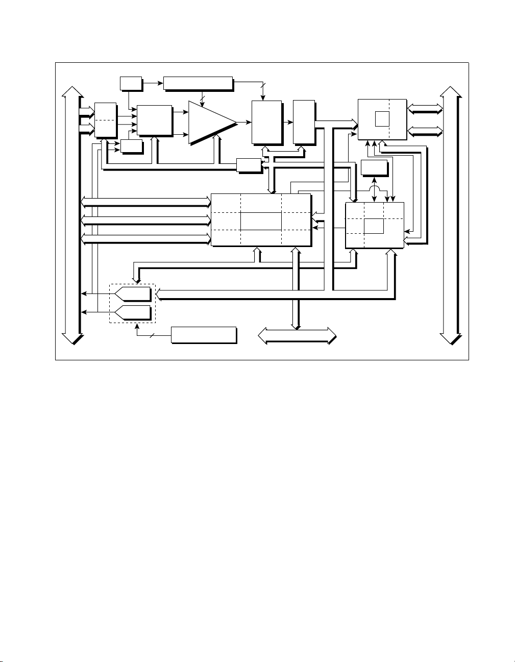
Figures
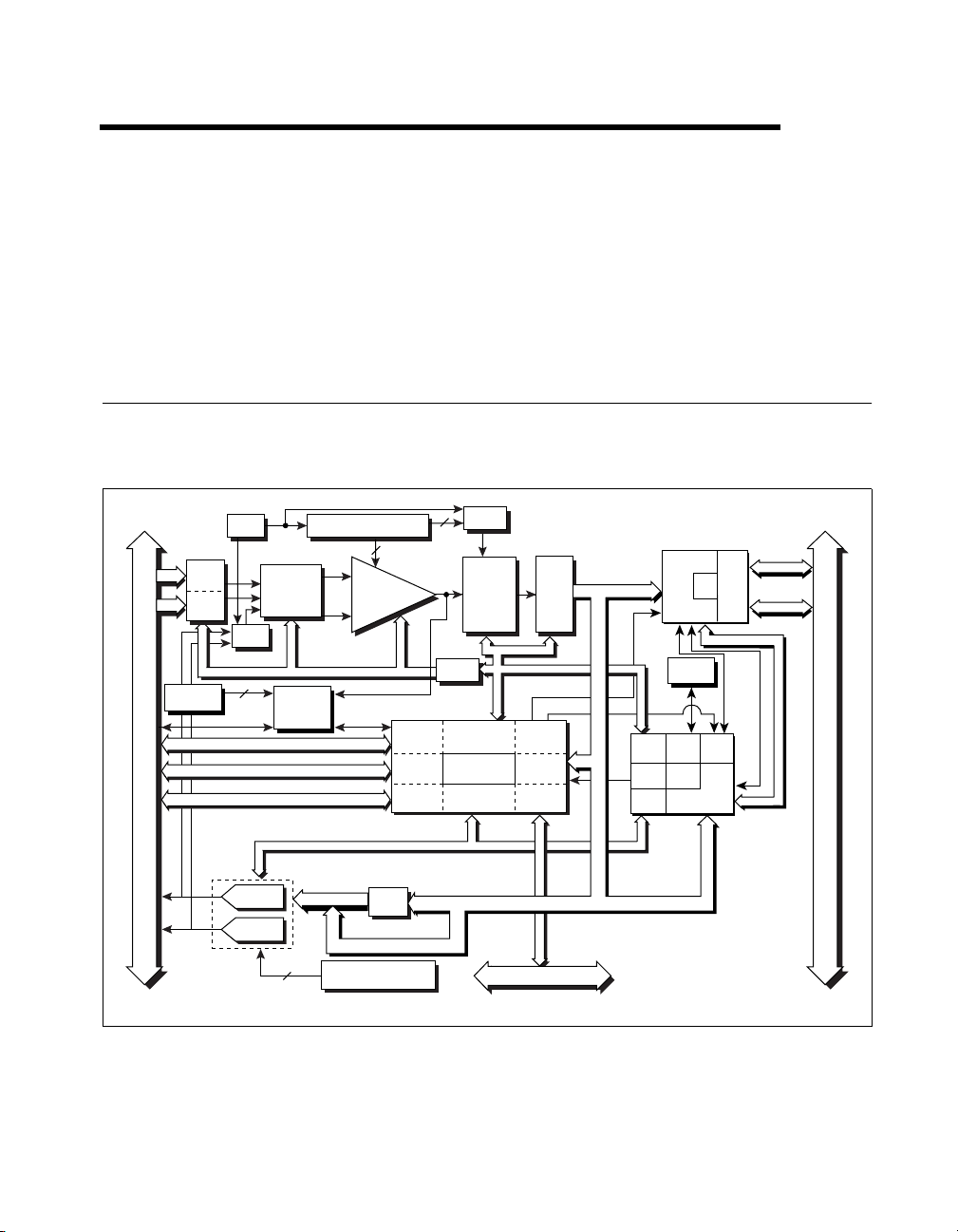
Figure 2-1. PCI-MIO-16E-1, PCI-MIO-16E-4, and PCI-6071E Block Diagram ..... 2-1
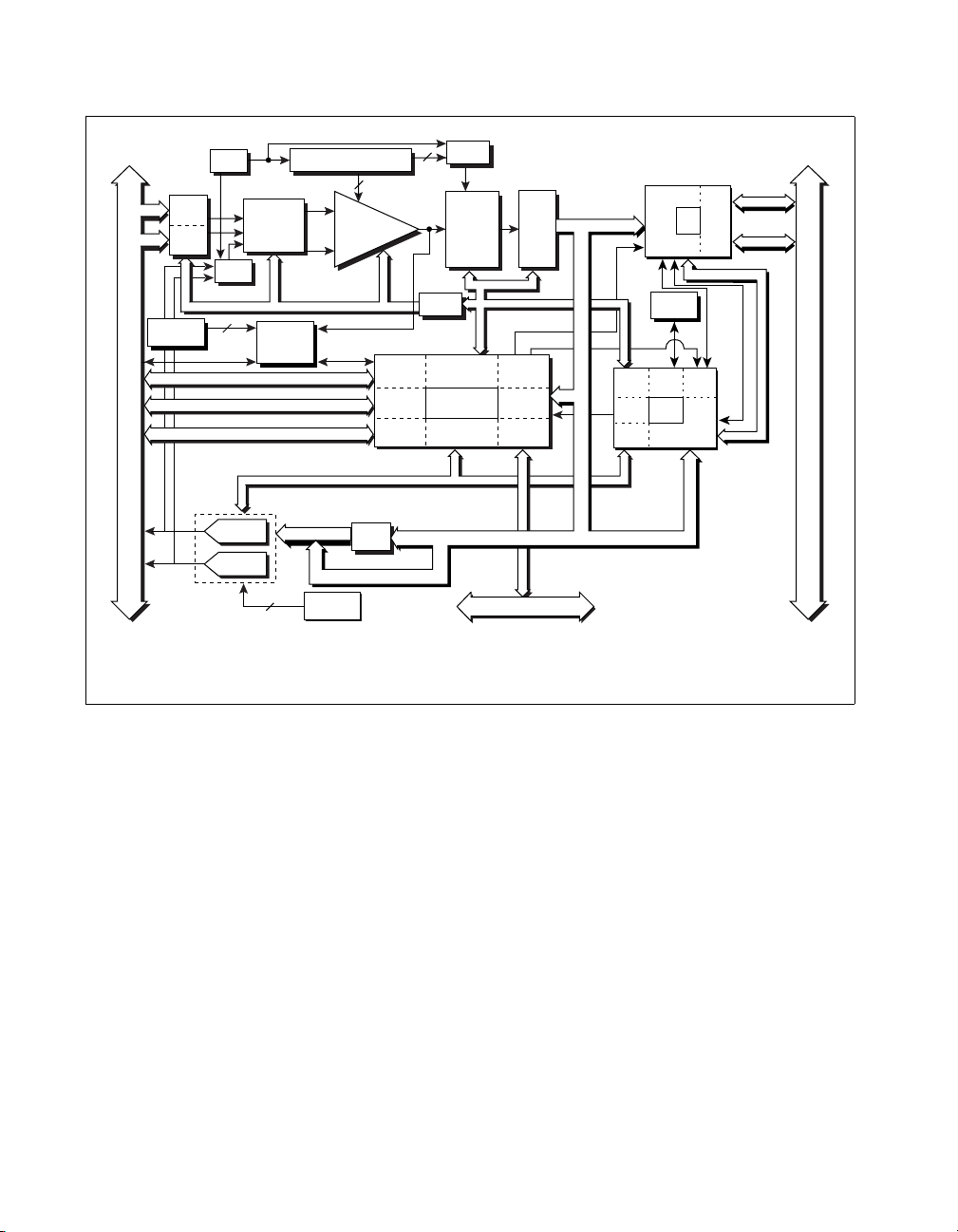
Figure 2-2. PCI-MIO-16XE-10, PCI-6052E, and PCI-6031E Block Diagram......... 2-2
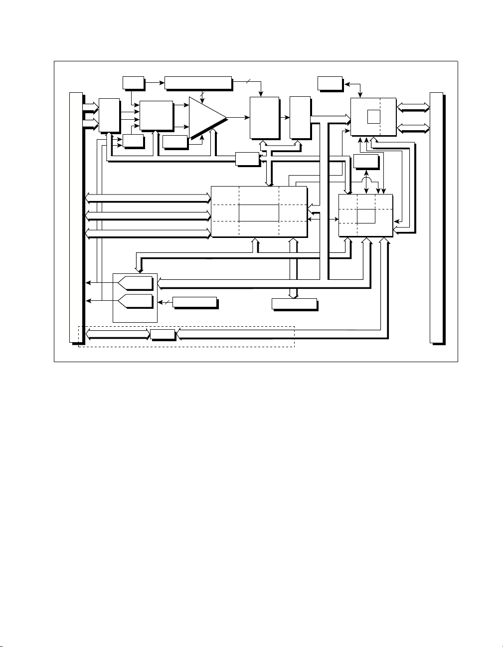
Figure 2-3. PCI-6023E, PCI-6024E, and PCI-6025E Block Diagram ...................... 2-3
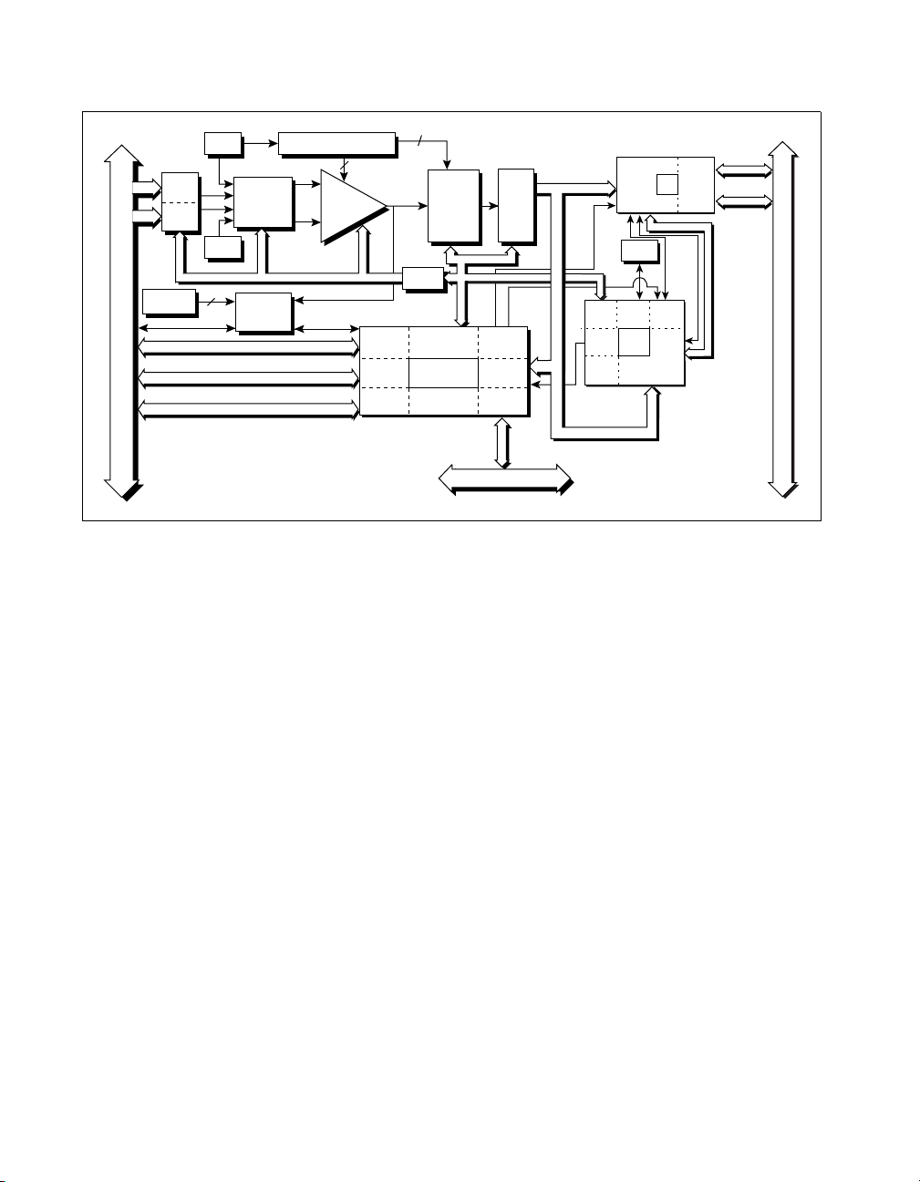
Figure 2-4. PCI-6032E and PCI-6033E Block Diagram ........................................... 2-4
Figure 2-5. PCI-MIO-16XE-50 Block Diagram........................................................2-5
Figure 2-6. PCI Bus Interface Circuitry Block Diagram...........................................2-7
Figure 2-7. Analog Input and Data Acquisition Circuitry Block Diagram ............... 2-8
Figure 2-8. ADC Timing ............................. ..............................................................2-12
Figure 2-9. Timing of Scan in Example 1 .................................................................2-14
Figure 2-10. Multirate Scanning of Two Channels.....................................................2-15
Figure 2-11. Multirate Scanning of Two Channels with 1:x Sampling Rate...............2-15
Figure 2-12. Multirate Scanning of Two Channels with 3:1:1 Sampling Rate ........... 2-16
Figure 2-13. Multirate Scanning of Three Channels with 4:2:1 Sampling Rate .........2-16
Figure 2-14. Multirate Scanning without Ghost..........................................................2-17
Figure 2-15. Occurrences of Conversion on Channel 1 in Example 3........................ 2-17
Figure 2-16. Successive Scans Using Ghost................................................................ 2-17
Figure 2-17. Analog Output Circuitry Block Diagram................................................2-20
Figure 2-18. DAQ-STC Counter Diagram ..................................................................2-24
Figure 2-19. RTSI Bus Interface Circuitry Block Diagram ........................................ 2-26
Tables
Figure 4-1. Analog Trigger Structure........................................................................4-54
Figure 4-2. DMA Structure........................................................................................4-57
Figure 4-3. DMA Link Chaining Mode Structure.....................................................4-59
Figure 5-1. EEPROM Read Timing .......................................................................... 5-2
Figure 5-2. Calibration AC Write Timing.................................................................5-16
Table 2-1. PGIA Gain Set Verses Board ...............................................................2-9
Table 2-2. Analog Input Configuration Memory ..................................................2-18
Table 3-1. PCI E Series Register Map ..................................................................3-2
Table 3-2. PCI E Series Windowed Register Map.................................................3-3
Table 3-3. PGIA Gain Selection.............................................................................3-10
Table 3-4. Calibration Channel Assignments.........................................................3-12
Table 3-5. Differential Channel Assignments........................................................3-13
Table 3-6. Nonreferenced Single-Ended Channel Assignments ...........................3-13
Table 3-7. Referenced Single-Ended Channel Assignments..................................3-14
Table 3-8. Auxiliary Channel Assignments ...........................................................3-15
Table 3-9. Channel Assignments............................................................................3-15
PCI E Series RLPM viii
©
National Instruments Corporation
Page 8

Contents
Table 5-1. PCI-MIO-16E-1, PCI-MIO-16E-4, PCI-6071E EEPROM Map ..........5-3
Table 5-2. PCI-MIO-16XE-50 EEPROM Map .....................................................5-5
Table 5-3. PCI-MIO-16XE-10, PCI-6031E, PCI-6032E,
and PCI-6033E EEPROM Map ............................................................5-7
Table 5-4. PCI-6023E EEPROM Map ...................................................................5-9
Table 5-5. PCI-6024E and PCI-6025E EEPROM Map .........................................5-10
Table 5-6. PCI-6052E EEPROM Map ..................................................................5-12
Table 5-7. Type of CALDAC Used on Board .......................................................5-14
©
National Instruments Corporation ix PCI E Series RLPM
Page 9

About This Manual
This manual describes the registers and register map of the PCI E Series
boards and contains information concerning their register-level
programming.
The DAQ-STC, a National Instruments system timing controller ASIC, is
the timing engine that drives the PCI E Series boards. Consequently, the
timing and programming sections in this manual repeat certain information
from, or draw your attention to, sections in the DAQ-STC Technical
Reference Manual. You must use your register-level programmer manual
along with the DAQ-STC Technical Reference Manual for a complete
understanding of PCI E Series board programming.
Unless otherwise noted, text applies to all boards in the PCI E Series. The
PCI E Series boards are:
• PCI-MIO-16E-1
• PCI-MIO-16E-4
• PCI-MIO-16XE-10
• PCI-MIO-16XE-50
• PCI-6023E
• PCI-6024E
• PCI-6025E
• PCI-6031E (MIO-64XE-10)
• PCI-6032E (AI-16XE-10)
• PCI-6033E (AI-64XE-10)
• PCI-6052E
• PCI-6071E (MIO-64E-1)
The PCI E Series boards are high-performance multifunction analog,
digital, and timing I/O boards for the PCI bus computers. Supported
functions include analog input, analog output, digital I/O, and timing I/O.
©
National Instruments Corporation xiii PCI E Series RLPM
Page 10

About This Manual
Organization of This Manual
The PCI E Series Register-Level Programmer Manual is organized as
follows:
• Chapter 1, General Description, describes the general characteristics
of the PCI E Series boards.
• Chapter 2, Theory of Operation, contains a functional overview of the
PCI E Series boards and explains the operation of each functional unit
making up the PCI E Series boards.
• Chapter 3, Register Map and Descriptions, describes in detail the
address and function of each of the PCI E Series control and status
registers.
• Chapter 4, Programming, contains programming instructions for
operating the circuitry on the PCI E Series boards.
• Chapter 5, Calibration, explains how to calibrate the analog input and
output sections of the PCI E Series boards by reading calibration
constants from the EEPROM and writing them to the calibration
DACs.
• Appendix A, Customer Communication, contains forms you can use to
request help from National Instruments or to comment on our products
and manuals.
• The Glossary contains an alphabetical list and description of terms
used in this manual, including abbreviations, acronyms, metric
prefixes, mnemonics, and symbols.
• The Index contains an alphabetical list of key terms and topics in this
manual, including the page where you can find each one.
Conventions Used in This Manual
The following conventions are used in this manual:
<> Angle brackets containing numbers separated by an ellipsis represent a
range of values associated with a bit or signal name—for example,
DBIO<3..0>.
This icon to the left of bold italicized text denotes a note, which alerts you
to important information.
PCI E Series RLPM xiv
©
National Instruments Corporation
Page 11

About This Manual
bold Bold text denotes the names of menus, menu items, parameters, dialog
boxes, dialog box buttons or options, icons, windows, Windows 95 tabs,
or LEDs.
bold italic Bold italic text denotes a note, caution, or warning.
italic Italic text denotes variables, emphasis, a cross reference, or an introduction
to a key concept. This font also denotes text from which you supply the
appropriate word or value, as in Windows 3.x.
Macintosh Macintosh refers to all Macintosh computers with the PCI bus, unless
otherwise noted.
monospace Text in this font denotes text or characters that you should literally enter
from the keyboard, sections of code, programming examples, and syntax
examples. This font is also used for the proper names of disk drives, paths,
directories, programs, subprograms, subroutines, device names, functions,
operations, variables, filenames and extensions, and for statements and
comments taken from programs.
PC PC refers to the IBM PC AT and compatible computers with the PCI bus.
Related Documentation
The following National Instruments manuals contain general information
and operating instructions for the PCI E Series boards:
• PCI E Series User Manual
• DAQ-STC Technical Reference Manual
• PCI-6023E/6024E/6025E User Manual
Customer Communication
National Instruments wants to receive your comments on our products
and manuals. We are interested in the applications you develop with our
products, and we want to help if you have problems with them. To make it
easy for you to contact us, this manual contains comment and configuration
forms for you to complete. These forms are in Appendix A, Customer
Communication, at the end of this manual.
©
National Instruments Corporation xv PCI E Series RLPM
Page 12

General Description
This chapter describes the general characteristics of the PCI E Series
boards.
General Characteristics
The PCI E Series boards are Plug and Play-compatible multifunction
analog, digital, and timing I/O boards for the PCI bus computers. This
family of boards features 12-bit and 16-bit ADCs with 16 and 64 analog
inputs, 12-bit and 16-bit DACs with voltage outputs, eight TTL-compatible
digital I/O, and two 24-bit counter/timers for timing I/O. Because the
PCI E Series boards have no DIP switches, jumpers, or potentiometers,
they are easily configured and calibrated using software. This feature is
made possible by the National Instruments MITE bus interface chip to
connect the boards to the PCI I/O bus. The MITE implements the PCI Local
Bus Specification so that the DMA, interrupts, and base address are all
software configurable.
1
Note
©
National Instruments Corporation 1-1 PCI E Series RLPM
Revision C and earlier versions of the PCI-MIO-16XE-50 use the MITE as the
interface chip and do not support the DMA feature.
The PCI E Series boards use the National Instruments DAQ-STC system
timing controller for time-related functions. The DAQ-STC consists of
three timing groups that control analog input, analog output, and
general-purpose counter/timer functions. These groups include a total of
seven 24-bit and three 16-bit counters and a maximum timing resolution
of 50 ns.
A common characteristic with DAQ boards is that you cannot easily
synchronize several measurement functions to a common trigger or timing
event. The PCI E Series boards have the Real-Time System Integration
(RTSI) bus to solve this problem. The RTSI bus consists of our RTSI bus
interface and a ribbon cable to route timing and trigger signals between
several functions on up to five DAQ boards in your PCI bus computer.
The PCI E Series boards can interface to an SCXI system so that you can
acquire over 3,000 analog signals from thermocouples, RTDs, strain
gauges, voltage sources, and current sources. You can also acquire or
Page 13

Chapter 1 General Description
generate digital signals for communication and control. SCXI is the
instrumentation front end for plug-in DAQ boards.
Y our PCI E Series board is completely software configurable. Refer to your
PCI E Series User Manual if you have not already installed and configured
your board.
PCI E Series RLPM 1-2
©
National Instruments Corporation
Page 14
Theory of Operation
This chapter contains a functional overview of the PCI E Series boards and
explains the operation of each functional unit making up the PCI E Series
boards.
Functional Overview
The block diagram in Figures 2-1 through 2-5 give a functional overview
of each PCI E Series board.
Analog
Trigger
Calibration
DACs
+
Programmable
Gain
Amplifier
–
3
Trigger
Counter/
Timing I/O
Digital I/O
2
Configuration
Memory
Timing/Control
DAQ - STC
Analog Output
Timing/Control
Voltage
REF
(8)*
Analog
Muxes
(8)*
Calibration
Mux
Trigger Level
DACs
I/O Connector
2
Trigger
PFI / Trigger
Timing
Digital I/O (8)
Mux Mode
Selection
Switches
Circuitry
REF
Buffer
12-Bit
Sampling
A/D
Converter
Analog Input
AI Control
DMA/
Interrupt
Request
Bus
Interface
RTSI Bus
Interface
ADC
FIFO
Data (16)
Data (16)
IRQ
DMA
Analog
Input
Control
DAQ-STC
Bus
Interface
Analog
Output
Control
Generic
Bus
Interface
EEPROM
EEPROM
Control
MIO
Interface
MINI
MITE
Interface
Interface
DMA
I/O
Bus
PCI
Bus
Interface
2
Control
Address/Data
Address (5)
PCI Bus
AO Control
DAC0
DAC1
4
Calibration
DACs
DAC
FIFO
Data (16)
RTSI Bus
*(32) for the PCI-6071E
Figure 2-1.
©
National Instruments Corporation 2-1 PCI E Series RLPM
PCI-MIO-16E-1, PCI-MIO-16E-4, and PCI-6071E Block Diagram
Page 15
Chapter 2 Theory of Operation
Voltage
REF
(8)*
Analog
Muxes
(8)*
Trigger Level
DACs
Trigger
PFI / Trigger
Digital I/O (8)
I/O Connector
Timing
Calibration
Mux
2
Mux Mode
Selection
Switches
Analog
Trigger
Circuitry
Calibration
DACs
+
Programmable
Gain
Amplifier
–
3**
Trigger
Counter/
Timing I/O
Digital I/O
2
Configuration
Memory
Analog Input
Timing/Control
DAQ - STC
Analog Output
Timing/Control
AO Control
REF
Buffer
16-Bit
Sampling
A/D
Converter
AI Control
DMA/
Interrupt
Request
Bus
Interface
RTSI Bus
Interface
ADC
FIFO
Data (16)
Data (16)
IRQ
DMA
Analog
Input
Control
DAQ-STC
Bus
Interface
Analog
Output
Control
Generic
Bus
Interface
EEPROM
EEPROM
Control
MIO
Interface
MITE
Interface
Interface
DMA
Bus
I/O
PCI
Bus
Interface
Control
Address/Data
Address (5)
PCI Bus
DAC0
DAC1
4***
* (32) for the PCI-6031E
** (6) for the PCI-6052E
*** (8) for the PCI-6052E
Calibration
DACs
DAC
FIFO
Data (16)
RTSI Bus
Figure 2-2. PCI-MIO-16XE-10, PCI-6052E, and PCI-6031E Block Diagram
PCI E Series RLPM 2-2
©
National Instruments Corporation
Page 16
Chapter 2 Theory of Operation
Voltage
REF
(8)
Analog
Input
Muxes
(8)
Calibration
Mux
PFI / Trigger
Timing
I/O Connector
Digital I/O
DIO (24)
DAC0
DAC1
NOT ON 6023E
Analog Output
Analog Mode
Multiplexer
AO Control
Generator
82C55A
Calibration
Dither
Calibration DACs
6
6025E Only
DACs
PGIA
3
DIO Control
Trigger
Interface
Counter/
Timing I/O
Digital I/O
1
Converter
Configuration
Memory
Analog Input
Timing/Control
DAQ - STC
Analog Output
Timing/Control
A/D
ADC
FIFO
AI Control
DMA/
Interrupt
Request
Bus
Interface
RTSI Bus
Interface
RTSI Connector
IRQ
DMA
EEPROM
Data
Analog
Input
Control
DAQ-STC
Bus
Interface
Generic
Bus
Interface
EEPROM
EEPROM
Control
DAQ-
APE
MINIMITE
Interface
DMA
Interface
I/O
Bus
Interface
Bus
PCI
Control
Address/Data
Address
PCI Connector
Figure 2-3. PCI-6023E, PCI-6024E, and PCI-6025E Block Diagram
©
National Instruments Corporation 2-3 PCI E Series RLPM
Page 17
Chapter 2 Theory of Operation
Voltage
REF
(8)*
Analog
Muxes
(8)*
Calibration
Mux
DACs
2
Trigger
PFI / Trigger
Timing
Digital I/O (8)
Trigger Level
I/O Connector
* (32) for the PCI-6033E
Mux Mode
Selection
Switches
Analog
Trigger
Circuitry
Calibration
DACs
+
NI-PGIA
Gain
Amplifier
–
2
3
Trigger
Counter/
Timing I/O
Digital I/O
Configuration
Memory
Analog Input
Timing/Control
DAQ - STC
Analog Output
Timing/Control
16-Bit
Sampling
A/D
Converter
AI Control
IRQ
DMA/
Interrupt
Request
Bus
Interface
RTSI Bus
Interface
ADC
FIFO
DMA
Data (16)
Analog
Input
Control
DAQ-STC
Bus
Interface
Analog
Output
Control
Generic
Bus
Interface
EEPROM
EEPROM
Control
MIO
Interface
Interface
Bus
Interface
RTSI Bus
Figure 2-4. PCI-6032E and PCI-6033E Block Diagram
MITE
DMA
I/O
PCI
Bus
Interface
Control
Address/Data
Address (5)
PCI Bus
PCI E Series RLPM 2-4
©
National Instruments Corporation
Page 18
Chapter 2 Theory of Operation
Voltage
REF
(8)
Analog
Muxes
(8)
Calibration
Mux
PFI / Trigger
Timing
I/O Connector
Digital I/O (8)
DAC0
DAC1
Mux Mode
Selection
Switches
4
Calibration
DACs
+
Programmable
Gain
Amplifier
–
Calibration
DACs
2
2
16-Bit
Configuration
Memory
Sampling
A/D
Converter
ADC
FIFO
AI Control
IRQ
Data (16)
DMA
Trigger
Counter/
Timing I/O
Digital I/O
Analog Input
Timing/Control
DAQ - STC
Analog Output
Timing/Control
AO Control
Data (16)
DMA/
Interrupt
Request
Bus
Interface
RTSI Bus
Interface
RTSI Bus
Figure 2-5. PCI-MIO-16XE-50 Block Diagram
Analog
Input
Control
DAQ-STC
Bus
Interface
Analog
Output
Control
Generic
Bus
Interface
EEPROM
EEPROM
Control
Interface
MIO
MITE
Interface
DMA
Interface
I/O
Bus
Interface
PCI
Bus
Control
Address/Data
Address (5)
PCI Bus
The following major components make up the PCI E Series boards:
• PCI bus interface circuitry with Plug and Play capability (MITE)
• Analog input circuitry
• Analog trigger circuitry
• Analog output circuitry
• Digital I/O circuitry
• Timing I/O circuitry (DAQ-STC)
• RTSI bus interface circuitry
The internal data and control buses interconnect the components. Notice
that the DA Q-STC is the timing engine that provides precise timing signals
for the analog input and output operations. The timing I/O circuitry
information in this manual is skeletal in nature and is sufficient in most
cases. For register-level programming information, refer to the DAQ-STC
Technical Reference Manual.
©
National Instruments Corporation 2-5 PCI E Series RLPM
Page 19

Chapter 2 Theory of Operation
PCI Interface Circuitry
The PCI E Series interface circuitry consists of a PCI interface chip and
a digital control logic chip. The PCI interface chip provides a mechanism
for the PCI E Series to communicate with the PCI bus. The digital control
logic chip connects the PCI interface chip with the rest of the board. The
PCI E Series is fully com pliant with PCI Local Bus Specification,
Revision 2.0. Therefore, the base memory address and the interrupt level
for the board are stored inside the PCI interface chip at power on. You do
not need to set any switches or jumpers. The PCI bus is capable of 8-bit,
16-bit, or 32-bit transfers, but PCI E Series boards use only 8-bit or
16-bit transfers.
The bus-mastering capabilities of the MITE provides high-speed data
transfer between the board and system memory. The MITE contains three
DMA channels that can be used simultaneously for data transfer with
analog input, analog output, and the general-purpose counters. The MITE
can control the PCI bus and transfer the data without interrupting the
host processor.
The DAQ-STC can generate interrupts from over 20 sources and can route
these interrupts to the INTA line on the PCI bus interface. Using two
interrupt lines, such as INTB, INTC or INTD, is not permitted for the
PCI E Series since each function in the PCI E Series does not have its own
configuration space. PCI E Series boards have the DAQ-STC IRQOUT0
line connected to the MITE interrupt input. Therefore, when setting up
interrupts you must route all interrupts through IRQOUT0. See the
DAQ-STC Technical Reference Manual for more information.
PCI E Series RLPM 2-6
©
National Instruments Corporation
Page 20
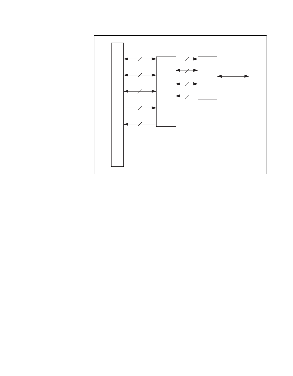
Data/Address Address
Chapter 2 Theory of Operation
Interface Control
Arbitration
System
PCI Bus
INTA
Figure 2-6. PCI Bus Interface Circuitry Block Diagram
Analog Input and Timing Circuitry
The PCI E Series boards have 16 and 64 analog input channels and a timing
core within the DAQ-STC that is dedicated to analog input operation.
Figure 2-7 shows a general block diagram for the analog input circuitry.
MITE
PCI
Interface
Chip
Data
Control
Interrupt
DAQ-STC
IRQOUT0
Control/Data
©
National Instruments Corporation 2-7 PCI E Series RLPM
Page 21
Chapter 2 Theory of Operation
AISense
ACH0
ACH1
ACH2
ACH3
ACH4
ACH5
ACH6
ACH7
ACH8
ACH9
ACH10
…
…
…
…
ACH15*
Input Multiplexer
Calibration
Sources
AIGND
Cal Mux
Mode
Selection
Channel
Type
Calibration
DACs
Dither
PGIA
ADC FIFO
Gain
Polarity
Convert
Channel
Number
*ACH63 for PCI-6071E, PCI-6031E, and PCI-6033E
Figure 2-7. Analog Input and Data Acquisition Circuitry Block Diagram
Analog Input Circuitry
The general model for analog input on the PCI E Series boards
includes input multiplexer, multipl e xer mode selection switches,
a software-programmable gain instrumentation amplifier, calibration
hardware, a sampling ADC, a 16-bit wide data FIFO, and a configuration
memory.
The configuration memory defines the parameters to use for each
conversion. Each entry in the conf iguration memory includes channel type,
channel number, bank, gain, polarity, dither, general trigger, and last
channel. The configuration memory is a 512-entry deep FIFO that is
initialized prior to the start of the acquisition sequence. It can be
incremented after every conversion, allowing the analog input
configuration to vary on a per conversion basis. Once the FIFO is empty,
PCI E Series RLPM 2-8
©
National Instruments Corporation
Page 22

Chapter 2 Theory of Operation
the DAQ-STC asserts the FIFO retransmit signal, which restores the FIFO
data to its original state.
The channel type field indicates the resource type to be used during
the conversion and controls the multiplexer mode selection switches.
These resources include calibration channels, analog input channels in
differential, referenced single-ended, or nonreferenced single-ended mode,
or a ghost channel. The ghost channel type indicates that a conversion
should occur but that the data should not be stored in the data FIFO. This
type is useful for multirate scanning, which is described later in
this chapter.
The channel number indicates which channel of the specified type will be
used during the conversion, while the bank field indicates which bank of
16 channels is active. This bank field is used on boards that hav e more than
16 channels. These bits control the input multiplexers.
The programmable gain instrumentation amplifier (PGIA) serves two
purposes on the PCI E Series boards. The PGIA applies gain to the input
signal, amplifying an analog input signal before sampling and conversion
to increase measurement resolution and accuracy. This gain is determined
by the gain field in the configuration memory. It also provides polarity
selection for the input signal, which is also controlled by the configuration
memory . In unipolar mode, the input range includes only positive voltages.
In bipolar mode, the input signal may also be a negative voltage. The
PGIA provides gains shown in Table 2-1.
Table 2-1. PGIA Gain Set Verses Board
Gain
PCI-MIO-16E-1
PCI-MIO-16E-4
PCI-6071E
PCI-6052E
PCI-MIO-16XE-50
PCI-MIO-16XE-50
PCI-6031E
PCI-6032E
PCI-6033E
PCI-6023E
PCI-6024E
PCI-6025E
0.5 ✓ — — ✓
1 ✓ ✓ ✓ ✓
2 ✓ ✓ ✓ —
5 ✓ — ✓ —
10 ✓ ✓ ✓ ✓
20 ✓ — ✓ —
©
National Instruments Corporation 2-9 PCI E Series RLPM
Page 23

Chapter 2 Theory of Operation
Table 2-1. PGIA Gain Set Verses Board (Continued)
Gain
PCI-MIO-16E-1
PCI-MIO-16E-4
PCI-6071E
PCI-6052E
PCI-MIO-16XE-50
PCI-MIO-16XE-50
PCI-6031E
PCI-6032E
PCI-6033E
PCI-6023E
PCI-6024E
PCI-6025E
50 ✓ — ✓ —
100 ✓ ✓ ✓ ✓
The dither circuitry adds approximately 0.5 LSB rms of white Gaussian
noise to the signal being converted by the ADC. This addition is useful
for applications, such as calibration, involving averaging to increase the
resolution of the board to more than the resolution of the ADC. In such
applications, which are often lower frequency in nature, adding the dither
decreases noise modulation and improves differential linearity. Dither
should be disabled for high-speed applications not involving averaging
because it would only add noise. When taking DC measurements, such as
when calibrating the board, you should enable dither and average about
1,000 points to take a single reading. This process removes the effects of
quantization, reduces measurement noise, and improves resolution. Notice
that dither cannot be disabled on the PCI-MIO-16XE-50,
PCI-MIO-16XE-10, PCI-6031E, PCI-6032E, PCI-6052E, or PCI-6033E.
The last channel bit is used to indicate that this is the last conversion in a
scan. The DAQ-STC will end the scan on the conversion with this bit set.
The PCI E Series boards use sampling, successive approximation ADCs
with 12 or 16 bits of resolution with maximum conversion rates between
50 µs and 800 ns. The converter can resolve its input range into 4,096
different steps for the 12-bit ADC and 65,536 for the 16-bit ADC. The input
range of the 12-bit boards is ±5 V in bipolar mode and 0 to +10 V in
unipolar mode. These modes correspond to ranges of –2,048 to 2,047 in
unipolar mode and 0 to 4,095 in bipolar mode. The input range of the 16-bit
boards is ±10 V in bipolar mode and 0 to +10 V in unipolar mode. These
modes correspond to ranges of –32,768 to 32,767 in bipolar mode and 0 to
65,535 in unipolar mode.
The PCI E Series boards include a 16-bit wide FIFO to buffer the analog
input data. This buffering will increase the maximum rate that the analog
input can sustain during continuous acquisition. The FIFO is 2,048 words
deep on the PCI-MIO-16XE-50, and 512 words deep on the other
PCI E Series boards. The DAQ-STC shifts the data into the FIFO from the
ADC when the conversion is complete. This buffering allows the ADC to
begin a new con version ev en though the data has not yet been read from the
PCI E Series RLPM 2-10
©
National Instruments Corporation
Page 24

Chapter 2 Theory of Operation
board. This buffering also pr o vides more time for the soft war e or DMA to
respond and read the analog input data from the board. If the FIFO is full
and another conversion completes, an error condition called FIFO overflow
occurs and the data from that conversion is lost. The FIFO not empty,
half-full, and full flags are available to generate interrupts or DMA requests
for the data transfer.
Measurement reliability is assured through the onboard calibration
circuitry of the board. This circuitry uses an internal, stable 5 V reference
that is measured at the factory against a higher accuracy reference; its
value is then stored in the EEPROM. With this stored reference value,
the board can be recalibrated at any time under any number of different
environmental conditions in order to remove errors caused by time and
temperature drift. The EEPROM stores calibration constants that can be
read and then written to calibration DACs that adjust input offset, output
offset, and gain errors associated with the analog input section. When the
board leaves the factory, the upper one-fourth of the EEPROM is protected
and cannot be overwritten. The lower three-fourths is unprotected, and the
top fourth of that can be used to store alternate calibration constants for the
different conditions under which you use the board.
Data Acquisition Timing Circuitry
This section describes the different methods of acquiring A/D data from a
single channel or multiple channels.
From this section through the end of this manual, you are assumed to have
a working knowledge of the DAQ-STC features. These features are
explained in the DAQ-STC Technical Reference Manual. If you have not
read the functional description of each DAQ-STC module, you must do so
before completing this register-level programmer manual.
Single-Read Timing
To acquire data from the ADC, initiate a single conversion and read the
resulting value from the ADC FIFO buffer after the conversion is complete.
You can generate a single conversion in three different ways—apply an
active pulse to the CONVERT* pin of the I/O connector, generate a falling
edge on the sample-interval counter of the DAQ-STC, or strobe the
©
National Instruments Corporation 2-11 PCI E Series RLPM
Page 25

Chapter 2 Theory of Operation
CONVERT*
ADC_BUSY*
SHIFTIN*
appropriate bit in a register in the PCI E Series register set. Any one of
these operations will generate the timing shown in Figure 2-8.
Figure 2-8. ADC Timing
When SHIFTIN* shifts the ADC value into the ADC FIFO buffer, the
AI_FIFO_Empty_St bit in the status register is cleared, which indicates
that valid data is av ailable to be read. Single conversion timing of this type
is appropriate for reading channel data on an ad hoc basis. However , if you
need a sequence of conversions, the time interval between successive
conversions is not constant because it relies on the softw are to generate the
conversions. For finely timed conversions that require triggering and
gating, you must program the boards to automatically generate timed
signals that initiate and gate conversions. This is known as a data
acquisition (DAQ) sequence.
Data Acquisition Sequence Timing
The following counters are used for a data acquisition sequence:
• Scan interval (SI) 24 bits
• Sample interval (SI2) 16 bits
• Divide by (DIV) 16 bits
• Scan counter (SC) 24 bits
This section presents a concise summary of only the most important
features of your board. For a complete description of all the analog input
modes and features of the PCI E Series boards, refer to the DAQ-STC
Technical Reference Manual.
The most basic timing signal in the analog input model is the CONVERT*
signal. A group of precisely timed CONVERT* pulses is a SCAN. The
sequence of channels selected in each conversion in a SCAN is
programmed in the configuration memory prior to starting the operation.
The SI2 counter is a 16-bit counter in the DAQ-STC. This counter
PCI E Series RLPM 2-12
©
National Instruments Corporation
Page 26

Chapter 2 Theory of Operation
determines the interval between CONVERT* pulses. It can be programmed
for a maximum interval of 3.3 ms and a minimum interval of 50 ns. If
alternate slow timebases are used, the maximum interval is 0.65 s. Each
time the counter reaches terminal count (TC), a CONVERT* pulse is
generated. Alternatively, CONVERT* pulses could be given externally.
A SCAN sequence is started by the ST AR T pulse, which is generated by the
TC of the SI counter. This counter is a 24-bit counter that determines the
time between the start of each SCAN. The minimum duration is 50 ns and
the maximum duration is 0.8 s when the internal 20 MHz timebase is used.
If the internal 100 kHz timebase is used, the maximum is 167 s. The ST ART
pulse triggers the SI2 counter to generate CONVERT* pulses. With each
conversion, the conf iguration memory advances by one and selects the next
set of analog input conditions—channel number, gain, polarity, etc. A
STOP pulse ends the SCAN sequence. This STOP could be generated in
two ways—either by using the LASTCHANNEL bit in the configuration
memory or by programming the 16-bit DIV counter to count the number of
conversions per SCAN and using the terminal count of the DIV counter as
a STOP pulse.
The SC is a 24-bit counter that counts the number of scans. The data
acquisition sequence can be programmed to stop when the terminal count
of this counter is reached. Notice that the START and STOP signals could
also be supplied externally.
Example 1: To acquire 50 scans, with each scan consisting of one sample
on channel 0 at gain 50, one sample on channel 5 at gain 2, and one sample
on channel 3 at gain 10, with a SCAN interval of 100 µs and a sample
interval of 10 µs, program your configuration memory as follows:
1. Channel 0, gain 50
2. Channel 5, gain 2
3. Channel 3, gain 10, last channel
You should program SI2 for 10 µs, SI for 100 µs, and SC for 50 scans.
©
National Instruments Corporation 2-13 PCI E Series RLPM
Page 27

Chapter 2 Theory of Operation
START
(TC of SI)
Figure 2-9 shows the timing for each scan in Example 1.
100 µs
10 µs
CONVERT
STOP
(last channel
or DIV TC)
Channel 0 Channel 5
Channel 3
Figure 2-9. Timing of Scan in Example 1
The START pulse starts each scan. The first CONVERT pulse samples
channel 0, the second CONVERT pulse samples channel 5, and the third
CONVERT pulse samples channel 3. The STOP pulse ends the scan.
Example 1 allows you to sample all three channels at a rate of 10 kS/s per
channel (100 µs sample interval period). To achieve different rates for
different channels, you must do multirate scanning.
Multirate Scanning without Using Ghost
Example 2: To sample channel 0 at 10 kS/s and channel 1 at 5 kS/s, both at
gain 1 with 50 scans, program the configuration memory as follows:
1. Channel 0, gain 1
2. Channel 1, gain 1, last channel
3. Channel 0, gain 1, last channel
PCI E Series RLPM 2-14
©
National Instruments Corporation
Page 28
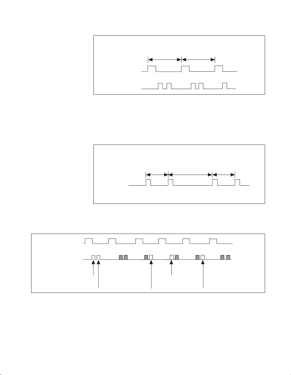
Chapter 2 Theory of Operation
Program SI for 100 µs, SI2 for 10 µs. Figure 2-10 shows the timing
sequence for two scans.
Sampling Rate
Channel 0: Channel 1 = 2:1
START
CONVERT
Channel 0Channel 0 Channel 1
STOP
Figure 2-10. Multirate Scanning of Two Channels
This sequence of two scans is repeated 25 times to complete the acquisition.
Notice that channel 0 is sampled once every 100 µs. Hence, its sampling
rate is 10 kS/s, whereas channel 1 is sampled once every 200 µs. Its rate is
5 kS/s. Similarly, you could implement an y 1:x ratio of sampling rates. The
1
effective scan interval of the slower channel will be at the rate of the
-- -
x
faster channel. This implementation requires x scan sequences in the
configuration memory.
Also, you can implement a 1:1:x or 1:x:mx ratio for three channels, where
m is a non-negative integer. Figures 2-11, 2-12, and 2-13 show timing
sequences for different ratios. In these figures, the numbers above the
CONVERT pulses indicate the channels sampled in that conversion.
Sampling Rates
Channel 0: Channel 1 = 5:1
START
CONVERT
STOP
0
Figure 2-11. Multirate Scanning of Two Channels with 1:
©
National Instruments Corporation 2-15 PCI E Series RLPM
00
0
001
x
Sampling Rate
Page 29
Chapter 2 Theory of Operation
Sampling Rates
Channel 0: Channel 1: Channel 2 = 3:1:1
START
CONVERT
STOP
Sampling Rates
Channel 0: Channel 1: Channel 2 = 4:2:1
START
CONVERT
0 0 01 2
Figure 2-12. Multirate Scanning of Two Channels with 3:1:1 Sampling Rate
Here, channel 0 is sampled three times, whereas channels 1 and 2 are
sampled once every three scans.
0
000121
STOP
Figure 2-13. Multirate Scanning of Three Channels with 4:2:1 Sampling Rate
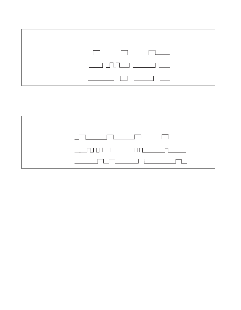
Multirate Scanning Using Ghost
If the ghost option in the configuration memory is set, that conversion
occurs but the data is not stored in the analog input FIFO. In other words,
a conversion is performed and the data is thrown away. By using this
option, multirate scanning with ratios such as x:y are possible, within the
limits imposed by the size of the configuration memory.
Figures 2-14 and 2-16 illustrate the advantages of using the ghost feature.
Figure 2-15 shows Example 3 timing, and Figure 2-16 shows the same
example using ghost.
Example 3: channel 1: channel 0 = 2:3 (without ghost).
PCI E Series RLPM 2-16
©
National Instruments Corporation
Page 30
Chapter 2 Theory of Operation
Sampling Rates
Channel 0: Channel 1 = 3:2
Start
Convert
0
t
1
t
1
0
0
Figure 2-14. Multirate Scanning without Ghost
In Example 3, channel 0 is sampled correctly. Although channel 1 is
sampled twice, it does not yield a 50% duty cycle. This type of acquisition
will result in imprecise rates. Figure 2-15 shows the relative occurrences of
convert pulses in Figure 2-14.
Channel 1, Example 3
t2t
Convert
t
Figure 2-15. Occurrences of Conversion on Channel 1 in Example 3
To rectify the problem, use ghost as illustrated in Figure 2-16.
Start
Convert
01 01 01 01 01 01
Figure 2-16. Successive Scans Using Ghost
The shaded conversions are ghost conversions. The short arrows indicate
channel 0 samples and the long arrows indicate channel 1 samples that are
actually stored in the FIFOs.
©
National Instruments Corporation 2-17 PCI E Series RLPM
Page 31

Chapter 2 Theory of Operation
Table 2-2 shows what the configuration memory should look like.
Table 2-2.
Analog Input Configuration Memory
Channel Ghost Last Channel
0 — —
1 — last channel
0 ghost —
1 ghost last channel
0 ghost —
1 — last channel
0 — —
1 ghost last channel
0 ghost —
1 — last channel
0 ghost —
1 ghost last channel
Now both channel 0 and channel 1 are sampled with 50% duty cycle.
Posttrigger and Pretrigger Acquisition
Whereas a data acquisition operation normally ends when the SC counts
down to zero, it can be initiated either through software, by strobing a bit
in a control register in the DAQ-STC, or by suitable external triggers.
There are two internal trigger lines—START1 and START2. These appear
at the connector on pins called PFI0/Trig1 and PFI1/Trig2, respectively.
ST AR T1 is used as a trigger line in the posttrigger mode. Since the ST AR T1
pulse can be generated through software by strobing a bit, all of the
examples discussed so far can be generally categorized as posttrigger
acquisition. In the classic posttrigger mode case, the data acquisition
circuitry is armed by software but does not start acquiring data until a pulse
is given on the START1 line. Then the acquisition starts and ends when the
SCAN counter counts down to zero.
In the pretrigger mode, data is acquired before and after the trigger. In this
mode, both START1 and ST ART2 lines are used. There are two counts for
PCI E Series RLPM 2-18
©
National Instruments Corporation
Page 32

Chapter 2 Theory of Operation
the SCAN counter—the pretrigger count and the posttrigger count. To
begin with, the pretrigger count is loaded into the SC. Acquisition is then
started through either software by strobing a bit, or through hardware by
externally pulsing the ST AR T1 pin of the connector. Acquisition then starts
and data is acquired. When the SC counts down to zero, the scans continue
and data still gets acquired. During this time, the board waits for a STAR T2
pulse but the SC does not count. Also, the SC gets loaded with the
posttrigger count. When a START2 pulse is received, the SC once again
starts counting. When it reaches zero, the operation ends. Refer to the
Acquisition Level Timing and Control section of Chapter 2 in the DAQ-STC
Technical Reference Manual for timing examples of pretrigger and
posttrigger modes.
Variations:
• Posttrigger and pretrigger modes can be retriggerable. This means
that after one posttrigger or pretrigger operation is over, the SC gets
reloaded and the board sits waiting for an additional START1. This
can continue indefinitely and can be disabled through software.
• A special mode in the DAQ-STC allows continuous software-initiated
acquisition to continue indefinitely . In this mode, the SC gets reloaded
each time it counts down to zero. The acquisition can be stopped by
disarming the SC. When the SC counts down to zero, acquisition stops.
Analog Triggering
All PCI E Series boards except the PCI-MIO-16XE-50, PCI-6023E,
PCI-6024E, and PCI-6025E have an analog trigger in addition to the digital
triggers. To use analog triggering to start an acquisition sequence, select
either the PFI0/Trig1 input on the I/O connector or one of the analog input
pins. An analog input pin allows you to apply gain to the external signal for
more flexible triggering conditions. The INT/EXTTRIG bit in the Misc.
Command Register selects the source. PFI0/Trig1 pin has an input voltage
range of ±10 V.
An 8-bit serial DAC sets each of the high and low thresholds in the
PCI-MIO-16E-1, PCI-6071E, and the PCI-MIO-16E-4. For the
PCI-MIO-16XE-10, PCI-6031E, PCI-6032E, and PCI-6033 E, a 12-bit
serial DAC sets each of the high and low thresholds. These thresholds are
within plus/minus full scale. The selected input is compared against each
of these thresholds by a comparator. The outputs of the comparators are
connected to the DAQ-STC analog trigger inputs 0 and 1. Within the
DA Q-STC, these signals can be routed to any of the internal timing signals.
You can trigger on either a positive or negative slope or on absolute values.
©
National Instruments Corporation 2-19 PCI E Series RLPM
Page 33

Chapter 2 Theory of Operation
Refer to the DAQ-STC Technical Reference Manual and the NI-DAQ
Function Reference Manual for more information on analog triggering.
For a detailed description of these modes, and timing diagrams, and for a
description of other modes not discussed here, refer to the DAQ-STC
Technical Reference Manual.
Analog Output and Timing Circuitry
The PCI E Series boards (except the PCI-6023E, PCI-6032E and
PCI-6033E) have two analog output channels and a timing core within the
DAQ-STC that is dedicated to analog output operation. Figure 2-17 shows
a general block diagram for the analog output circuitry.
LDAC0*
DAQ-STC
DAC0WR*
LDAC1*
DAC1WR*
Data Bus
FIFO DAC0
FIFO
Bypass
+10 V Reference
Figure 2-17.
Analog Output Circuitry Block Diagram
DAC1
MUX
MUX
DAC0OUT
I/O Connector
DAC1OUT
Extref
PCI E Series RLPM 2-20
©
National Instruments Corporation
Page 34

Chapter 2 Theory of Operation
Analog Output Circuitry
The general model for analog output on the PCI E Series boards includes
two channels of double-buffered analog output with programmable
polarity, reference source, and reglitching circuit, as well as a FIFO to
buffer the data. However, not all of the PCI E Series boards contain every
one of these features.
Each analog output channel contains a 12-bit DA C, an amplif ication stage,
and an onboard voltage reference, except for the PCI-MIO-16XE-10,
PCI-6052E, and PCI-6031E, which have a 16-bit DA C. The output voltage
will be proportional to the voltage reference (Vref) multiplied by the digital
code loaded into the DAC. Note that the output will be set to 0 V on power
up. The polarity, reference source, and reglitching circuit are all configured
in the AO Configuration Register.
The voltage reference source for each DAC is selectable from the onboard
reference or a voltage supplied at the EXTREF pin on the I/O connector,
except for the PCI-MIO-16XE-50, PCI-MIO-16XE-10, PCI-6024E,
PCI-6025E, and PCI-6031E which only supports the onboard reference.
The onboard reference is fixed at +10 V. The external reference can be
either a DC or an AC signal. If you apply an AC reference, the analog
output channel acts as a signal attenuator and the AC signal appears at the
output attenuated by the digital code. For unipolar output the voltage is
simply attenuated. Four quadrant multiplication occurs in bipolar output,
where the signal will not only be attenuated but also inverted for negative
digital codes.
The DAC output can be configured to produce either a unipolar or bipolar
output range, except for the PCI-MIO-16XE-50, which supports only
bipolar output. A unipolar output has an output range of 0 to +Vref
–1 LSB V. A bipolar output has an output voltage range of –Vref to
Vref –1 LSB V). For unipolar output, the data written to the DAC is
interpreted in straight binary format. For bipolar output, the data is
interpreted as two’s complement format. One LSB is the v oltage increment
corresponding to an LSB change in the digital code word. For a 12-bit
DA C, 1 LSB = (Vref)/4,096 in unipolar mode, and 1 LSB = (Vref)/2,048 in
bipolar mode. For a 16-bit DA C, 1 LSB = (Vref)/65,536 in unipolar mode,
and 1 LSB = (Vref)/32,768 in bipolar mode.
Using the 12-bit DAC and onboard 10 V reference will produce an output
voltage range of 0 to 9.9976 V in steps of 2.44 mV for unipolar output and
an output voltage range of –10 to +9.9951 V in steps of 4.88 mV for bipolar
operation. Using 16-bit DAC and onboard 10 V reference will produce an
output range of 0 to 9.9998 V in steps of 153 µV for unipolar output and an
©
National Instruments Corporation 2-21 PCI E Series RLPM
Page 35

Chapter 2 Theory of Operation
output voltage range of –10 to 9.9997 V in steps of 305 µV for bipolar
operation.
In normal operation, a DAC output will glitch whenever it is updated
with a new value. The glitch energy differs from code to code and appears
as distortion in the frequency spectrum. Each analog output of the
PCI-MIO-16E-1, PCI-6052E, and PCI-6071E contains a reglitch circuit
that generates uniform glitch energy at ev ery code rather than large glitches
at the major code transitions. This uniform glitch energy appears as a
multiple of the update rate in the frequency spectrum. Notice that this
reglitch circuit does not eliminate the glitches; it only makes them more
uniform in size.
The PCI-MIO-16E-1, PCI-MIO-16XE-10, PCI-6031E, PCI-6052E, and
PCI-6071E include 2 kword-deep FIFOs to buffer the analog output data.
The PCI-MIO-16E-4 has 512 word-deep FIFOs. This buffering will
increase the maximum rate that the analog output can sustain for waveform
generation. It can also be used to store a complete waveform which can be
output repetitively without any further data transfer to the FIFO. The
PCI-MIO-16XE-50, PCI-6024E, and PCI-6025E has a zero-depth virtual
FIFO.
Analog Output Timing Circuitry
This section describes the different methods of setting the analog output
voltage, including single-point updating and waveform generation. The
DAQ-STC provides the timing signals necessary to write to the DACs and
update them.
The DACs are double buffered and can be individually configured for
immediate update or timed update mode. In immediate update mode, the
double buffering of the DAC is disabled and the value written to the DAC
will appear immediately on the output after the write completes. In the
timed update mode, the double buffering is enabled. When double
buffering is enabled, writing the digital value loads that value into the buffer
stage of the DAC. When an update signal is received, the analog output of
the DAC changes.
Single-Point Output
The data values can be written directly to the DACs under software control
without the use of the timing engine provided in the DAQ-STC. This is
typically useful for setting the analog outputs to DC levels, where precise
timing of the output change is not important. Writing directly to the DACs
is accomplished by writing the desired value to the DAC<0..1> Direct Data
PCI E Series RLPM 2-22
©
National Instruments Corporation
Page 36

Chapter 2 Theory of Operation
Register. This action will store the value in the first buffer of the DAC. If
the DAQ-STC is programmed for immediate updating mode, the value will
also be applied to the analog output. If the DAQ-STC is programmed for
timed updating mode, the appropriate update signal, LDAC0* or LDAC1*,
must be asserted by writing to the appropriate DAQ-STC register.
Waveform Generation
The timing engine in the DAQ-STC can be used for waveform generation,
where the update signals connected to the DACs can be generated at precise
intervals. In this model, the DAQ-STC will generate the update signals and
then transfer the data values for the next update to the first buffer of
the DACs.
The update interval counter (UI) is 24 bits wide and generates the update
pulses. These update pulses can be routed to the D ACs. The update counter
(UC) is 24 bits wide and counts the number of updates. The value loaded
into this counter defines a buffer. The buffer counter (BC) determines how
many times a buffer should be repeated. These counters define an analog
output sequence.
The DAQ-STC will transfer the data values for the next update after each
update pulse. This data transfer will be from the analog output FIFO. Some
of the boards have large 2 kword FIFOs and some have 512 word FIFOs;
others are zero-deep virtual FIFOs. The large FIFOs are true FIFOs, where
data can be written to the FIFOs as long as they are not full, and can be read
from when they are not empty . In this case, the DAQ-STC will transfer the
data from the FIFO to the DACs when the FIFO is not empty. If the FIFO
is empty, the DAQ-STC will delay the transfer until more data is written
into the FIFO.
The zero-deep virtual FIFOs are not true FIFOs, but they do provide a
software compatible method for waveform generation. When the
DAQ-STC generates an update signal and is ready to transfer data, the
board will clear the FIFO full flag. This FIFO full flag can be used by
interrupts or DMA to transfer data to the virtual FIFO. The virtual FIFO
will not actually buffer the data, instead it will transfer it directly to the first
buffer of the destination D AC. After the data has been transferred, the board
will set the FIFO full flag, indicating that no more data is required. Note
that the half-full and empty flags do not provide useful information for data
transfer and should not be used.
The large FIFOs can also be used to generate repetitive waveforms at
very high speeds and without using any bus bandwidth. The FIFOs can be
loaded with the desired waveform and the DAQ-STC can be programmed
©
National Instruments Corporation 2-23 PCI E Series RLPM
Page 37
Chapter 2 Theory of Operation
Digital I/O Circuitry
to retransmit the same FIFO data to the DACs over and over. When the
FIFO is empty, the retransmit signal is asserted, which restores that FIFO
data to its original state.
When both DA Cs are used in wa veform generation, the data in the FIFO is
interleaved; in other words, every alternate sample belongs to one DAC.
The PCI E Series boards have eight digital I/O lines. Each of the eight
digital lines can be individually programmed to be input or output, if used
in parallel. For serial data transfer, DIO4 is used as the serial data in pin,
and DIO0 is used as the serial data out pin.
You can use handshaking with the EXTSTROBE* pin to do either parallel
or serial data transfer. Refer to the DAQ-STC Technical Reference Manual
for more details on the DIO features.
The external strobe signal EXTSTROBE* is a general-purpose strobe
signal. Software can set the output of the EXTSTROBE* pin to either a
high or low state. EXTSTROBE* is not necessarily part of the digital I/O
circuitry , b ut is included here because you can use it to latch digital output
from the PCI E Series into an external device.
Timing I/O Circuitry
The DAQ-STC has two 24-bit general purpose counter/timers. The
counters are numbered 0 and 1 and are diagrammed as shown in
Figure 2-18.
Figure 2-18.
PCI E Series RLPM 2-24
SOURCE
Counter
OUT
GATE
UPDOWN
DAQ-STC Counter Diagram
©
National Instruments Corporation
Page 38

The counter counts the transitions, or edges, on the SOURCE line when the
GATE is enabled and generates timing signals at its OUT output pin. The
UPDOWN pin determines the direction of counting. Active polarities of
these pins are software selectable in the DAQ-STC. Notice that on the
PCI E Series boards only the SOURCE, GATE, and OUT pins are brought
out to the I/O connector. The UPDOWN pin for counter 0 is internally
connected to DIO6, and to DIO7 for counter 1. T o dri ve the UPDO WN pin
from the connector, you must tri-state the corresponding DIO line.
The SOURCE of these counters can be selected to be one of the 10 PFI
lines, the seven RTSI lines, the internal 20 MHz or 100 kHz timebases, or
the TC of the other counter. With the last option, the two counters can be
concatenated. Similarly, the GATE can also be selected from a variety of
different sources. The sources for both of these signals are described in the
DAQ-STC Technical Reference Manual.
RTSI Bus Interface Circuitry
The PCI E Series is interfaced to the National Instruments RTSI bus. The
RTSI bus has seven trigger lines and a system clock line. You can wire all
National Instruments PCI E Series boards with RTSI bus connectors inside
the PCI bus computer and share these signals. Figure 2-19 shows a block
diagram of the RTSI bus interface circuitry.
Chapter 2 Theory of Operation
©
National Instruments Corporation 2-25 PCI E Series RLPM
Page 39

Chapter 2 Theory of Operation
Trigger
RTSI Bus Connector
Clock
DAQ-STC
TRIG1
TRIG2
CONVERT*
UPDATE*
WFTRIG
GPCTR0_SOURCE
GPCTR0_GATE
GPCTR0_OUT
7
RTSI Switch
mux
STARTSCAN
AIGATE
SISOURCE
AOGATE
UISOURCE
AO2GATE
UI2SOURCE
GPCTR1_SOURCE
GPCTR1_GATE
RTSI_OSC (20 MHz)
Figure 2-19. RTSI Bus Interface Circuitry Block Diagram
The RTSI functionality is provided in the DAQ-STC chip. This RTSI
trigger module consists of seven 12-to-1 multiplexers that dri ve seven R TSI
Trigger bus signals and four 8-to-1 multiplexers that drive the four RTSI
board signals.
Any of the seven RTSI trigger bus signals can be driven by eight internally
generated timing signals and the four RTSI board signals. Similarly, the
four RTSI board signals can be driven by any of the RTSI trigger bus
signals. Of the four RTSI board signals, only one is used. By programming
certain bits in the DAQ-STC, you can drive the CONVERT pulse onto
RTSI_BRD0 and then onto any of the TRIGGER lines.
PCI E Series RLPM 2-26
©
National Instruments Corporation
Page 40

Register Map and Descriptions
This chapter describes in detail the address and function of each of the PCI E Series board
control and status registers.
If you plan to use an application software package such as NI-DAQ, LabVIEW, or
LabWindows/CVI with your PCI E Series board, you need not read this chapter. However,
you gain added insight into your PCI E Series board by reading this chapter.
Register Map
T able 3-1 shows the register map for the PCI E Series boards and gives the register name, the
register offset address, the type of the register (read-only, write-only, or read-and-write), and
the size of the register in bits. Obtain the actual register address by adding the appropriate
register offset to the memory base address of the PCI E Series board.
Registers are grouped in the table by function. Each register group is introduced in the order
shown in Table 3-1, then described in detail, including a bit-by-bit description.
The DAQ-STC has 180 different registers. The more frequently used registers have been
given lower offset addresses an d are shown in Table 3-1 as the DAQ-STC Register Group.
The advantage of having lower offset addresses is that they can be accessed directly or
through the DAQ-STC windowed mode. You can access the remaining registers in the
DA Q-STC only in the windowed mode. In this mode, the address of the register is first written
to the Window Address Register. The data to be written is then written to the Window Data
Register . Using windowed mode has the adv antage of reducing the address space of the board
from 180 to 32 bytes. However, this reduced address space is at the cost of two write
operations to write data to or two read operations to read data from a register.
3
©
National Instruments Corporation 3-1 PCI E Series RLPM
Page 41

Chapter 3 Register Map and Descriptions
Table 3-1. PCI E Series Register Map
Offset Address
Register Name
Misc Register Group
Serial Command
Misc Command
Status
Analog Input Register Group
ADC FIFO Data Register
Configuration Memory Low
Configuration Memory High
Analog Output Register Group
AO Configuration
DAC FIFO Data
DAC0 Direct Data
DAC1 Direct Data
DMA Control Register Group
AI AO Select
G0 G1 Select
DAQ-STC Register Group
Window Address
Window Data
Interrupt A Acknowledge
Interrupt B Acknowledge
AI Command 2
AO Command 2
G0 Command
G1 Command
AI Status 1
AO Status 1
G Status
AI Status 2
AO Status 2
DIO Parallel Input
0D
0F
01
1C
10
12
16
1E
18
1A
09
0B
0
2
4
6
8
A
C
E
4
6
8
A
C
E
13
15
1
28
16
18
22
30
24
26
9
11
0
2
4
6
8
10
12
14
4
6
8
10
12
14
Type SizeHex Decimal
Write-only
Write-only
Read-only
Read-only
Write-only
Write-only
Write-only
Write-only
Write-only
Write-only
Write-only
Write-only
Read-and-write
Read-and-write
Write
Write
Write
Write
Write
Write
Read
Read
Read
Read
Read
Read
8-bit
8-bit
8-bit
16-bit
16-bit
16-bit
16-bit
16-bit
16-bit
16-bit
8-bit
8-bit
16-bit
16-bit
16-bit
16-bit
16-bit
16-bit
16-bit
16-bit
16-bit
16-bit
16-bit
16-bit
16-bit
16-bit
PCI E Series RLPM 3-2
©
National Instruments Corporation
Page 42

Chapter 3 Register Map and Descriptions
Table 3-2.
Register Name
FIFO Strobe Register Group
Configuration Memory Clear
ADC FIFO Clear
DAC FIFO Clear
Register Sizes
Two different transfer sizes for read-and-write operations are available on the
computer—byte (8-bit) and word (16-bit). Table 3-1 shows the size of each PCI E Series
register. For example, reading the ADC FIFO Data Register requires a 16-bit (word) read
operation at the selected address, whereas writing to the Misc Command Register requires
an 8-bit (byte) write operation at the selected address. For proper board operation you must
adhere to these register size accesses. Avoid performing a byte access on a word location or
performing a word access on a byte location; these are invalid operations. The register sizes
are very important.
Register Descriptions
This section discusses each of the PCI E Series registers in the order shown in Table 3-1. Each
register group is introduced, followed by a detailed bit description. The individual register
description gives the address, type, word size, and bit map of the register, followed by a
description of each bit.
PCI E Series Windowed Register Map
Offset Address
52
53
54
82
83
84
Write-only
Write-only
Write-only
Type SizeHex Decimal
16-bit
16-bit
16-bit
The register bit map shows a diagram of the register with the MSB shown on the left (bit 15
for a 16-bit register, bit 7 for an 8-bit register), and the LSB shown on the right (bit 0). A
square represents each bit and contains the bit name. An asterisk (*) after the bit name
indicates that the bit is inverted (negative logic).
In many of the registers, several bits are labeled Reserved. When a re gister is read, these bits
may appear set or cleared but should be ignored because they have no signif icance. When you
write to a register, set these bits to zero.
Misc Register Group
The three registers making up the Misc Register Group include two command registers that
control the serial DACs, EEPROM, and analog trigger source, and one status register that
includes EEPROM information.
Bit descriptions of the three registers making up the Misc Register Group are given on the
following pages.
©
National Instruments Corporation 3-3 PCI E Series RLPM
Page 43

Chapter 3 Register Map and Descriptions
Serial Command Register
The Serial Command Register contains six bits that control PCI E Series serial EEPROM and
DACs. The contents of this register are cleared upon power up and after a reset condition.
Address: Base address + 0D (hex)
Type: Write-only
Word Size: 8-bit
Bit Map:
7 6 5 4 3 2 1 0
Reserved Reserved SerDacLd2 SerDacLd1 SerDacLd0 EEPromCS SerData SerClk
Bit Name Description
7–6 Reserved Reserved—Always write 0 to these bits.
5 SerDacLd2 Serial DAC Load2—This bit is used to load the third set of
serial DACs with the serial data previously shifted into the
DACs.
4 SerDacLd1 Serial DAC Load1—This bit is used to load the second set
of serial DACs with the serial data previously shifted into
the DACs.
3 SerDacLd0 Serial DAC Load0—This bit is used to load the first set of
serial DACs with the serial data previously shifted into the
DACs.
2 EEPromCS EEPROM Chip Select—This bit controls the chip select of
the onboard EEPROM used to store calibration constants.
When EEPromCS is set, the chip select signal to the
EEPROM is enabled.
1 SerData Serial Data—This bit is the data for the onboard serial
devices—the calibration EEPROM and the serial DACs.
This bit should be set to the desired value pri or to the
active write to the SerClk bit.
0 SerClk Serial Clock—This bit is the clock input to the onboard
serial devices. In order to access these devices, this bit is
used to clock data in or out as appropriate. See Chapter 5,
Calibration, for more information.
PCI E Series RLPM 3-4
©
National Instruments Corporation
Page 44

Chapter 3 Register Map and Descriptions
Misc Command Register
The Misc Command Register contains one bit that controls the PCI E Series analog trigger
source. The contents of this register are cleared upon power up and after a reset condition.
Address: Base address + 0F (hex)
Type: Write-only
Word Size: 8-bit
Bit Map:
7 6 5 4 3 2 1 0
Int/Ext Trig Reserved Reserved Reserved Reserved Reserved Reserved Reserved
Bit Name Description
7 Int/Ext Trig Internal/External Analog Trigger—This bit controls the
analog trigger source. If this bit is set, the output of the
PGIA2 is selected as the trigger source. If this bit is
cleared, the TRIG1 signal from the I/O connector is
selected as the trigger source.
6–0 Reserved Reserved—Always write 0 to these bits.
©
National Instruments Corporation 3-5 PCI E Series RLPM
Page 45

Chapter 3 Register Map and Descriptions
Status Register
The Status Register is used to indicate the status of the calibration EEPROM output.
Address: Base address + 01 (hex)
Type: Read-only
Word Size: 8-bit
Bit Map:
7 6 5 4 3 2 1 0
Reserved Reserved Reserved Reserved Reserved Reserved Reserved PROMOUT
Bit Name Description
7–1 Reserved Reserved—Ignore returned bits.
0 PROMOUT EEPROM Output Data—This bit reflects the serial output
data of the serial EEPROM.
PCI E Series RLPM 3-6
©
National Instruments Corporation
Page 46

Analog Input Register Group
The three registers making up the Analog Input Register Group control the analog input
circuitry and can be used to read the ADC FIFO contents. Reading the ADC FIFO Data
Register location transfers data from the PCI E Series ADC data FIFO to the computer.
Writing to the Configuration Memory Low and Configuration Memory High Register
locations sets up channel configuration information for the analog input section. This
information is necessary for single conversions as well as for single- and multiple-channel
data acquisition sequences.
Chapter 3 Register Map and Descriptions
©
National Instruments Corporation 3-7 PCI E Series RLPM
Page 47

Chapter 3 Register Map and Descriptions
ADC FIFO Data Register
The ADC FIFO Data Register returns the oldest ADC conversion value stored in the ADC
FIFO. Reading the ADC FIFO removes that value and leaves space for another ADC
conversion value to be stored. Values are shifted into the ADC FIFO whenever an ADC
conversion is complete unless the GHOST bit is set in that entry of the Configuration
Memory.
The ADC FIFO is emptied when all values it contains are read. The empty, half-full, and full
flags from the ADC data FIFO are available in a status re gister in the D AQ-STC. These flags
indicate when the FIFO is empty, half-full, or full, respectively. Whenever the FIFO is not
empty, the stored data can be read from the ADC FIFO Data register.
The values returned by reading the ADC Data Register are available in two different binary
formats: straight binary, which generates only positi ve numbers, or two’ s complement binary ,
which generates both positive and negative numbers. The binary format used is determined
by the mode in which the ADC is configured. Following is the bit pattern returned for
either format:
Address: Base address + 1C (hex)
Type: Read-only
Word Size: 16-bit
Bit Map:
15 14 13 12 11 10 9 8
D15 D14 D13 D12 D11 D10 D9 D8
7 6 5 4 3 2 1 0
D7 D6 D5 D4 D3 D2 D1 D0
Bit Name Description
15–0 D<15..0> Data bits 15 through 0—These bits are the result of the
ADC conversion. The boards with a 12-bit ADC return
values ranging from 0 to 4,095 decimal (0x0000 to
0x0FFF) when the ADC is in unipolar mode, and –2,048 to
2,047 decimal (0xF800 to 0x07FF) when the ADC is in
bipolar mode. The boards with a 16-bit ADC return values
ranging from 0 to 65,535 decimal (0x0000 to 0xFFFF)
when the ADC is in unipolar mode and 32,768 to 32,767
decimal (0x8000 to 0x7FFF) when the ADC is in bipolar
mode. The mode is controlled by the Unip/Bip bit in the
Configuration Memory Low Register.
PCI E Series RLPM 3-8
©
National Instruments Corporation
Page 48

Chapter 3 Register Map and Descriptions
Configuration Memory Low Register
The Configuration Memory Low Register works with the Configuration Memory High
Register to control the input channel selection multiplexers, gain, range, and mode settings.
The values written to these registers are placed into the Configuration Memory, which is
sequenced through during an acquisition. This register contains seven of these bits. The
contents of the Configuration Memory are emptied by a control register in the DAQ-STC.
Address: Base address + 10 (hex)
Type: Write-only
Word Size: 16-bit
Bit Map:
15 14 13 12 11 10 9 8
LastChan Reserved Reserved GenTrig Reserved Reserved DitherEn Unip/Bip
7 6 5 4 3 2 1 0
Reserved Reserved Reserved Reserved Reserved Gain2 Gain1 Gain0
Bit Name Description
15 LastChan Last Channel—This bit should be set in the last entry of
the scan sequence loaded into the channel configuration
memory. More than one occurrence of the LastChan bit is
possible in the configuration memory list for the
interval-scanning mode. For example, there can be
multiple scan sequences in one memory list.
14–13, Reserved Reserved—Always write 0 to these bits.
11–10,
7–3
12 GenTrig General Trigger—This bit synchronizes actions in the
DAQ-STC with the scan list. When this bit is set, an active
low trigger pulse is sent into the RTSI_BRD0 input of the
DAQ-STC during the CONVERT signal. This trigger is
used at the application level and can perform such actions
as time stamping and starting waveform generation.
9 DitherEn Dither Enable—This bit controls the dither circuitry
feeding the analog input. If this bit is set, approximately
±0.5 LSB of white Gaussian noise is added to the input
signal. This bit is reserved on the PCI-MIO-16XE-50,
©
National Instruments Corporation 3-9 PCI E Series RLPM
Page 49

Chapter 3 Register Map and Descriptions
8 Unip/Bip Channel Unipolar/Bipolar—This bit configures the ADC
2–0 Gain<2..0> Channel Gain Sele ct 2 through 0—These th ree bits control
PCI-MIO-16XE-10, PCI-6031E, PCI-6032E, and
PCI-6033E and should be set to 1. Dither cannot be
disabled on the PCI-MIO-16XE-50, PCI-MIO-16XE-10,
PCI-6031E, PCI-6032E, and PCI-6033E.
for unipolar or bipolar mode. When Unip/Bip is set, the
ADC is configured for unipolar operation and values read
from the ADC Data Register are in straight binary format.
When Unip/Bip is clear, the ADC is configured for bipolar
operation and values. The data values are two’s
complement and automatically sign extended.
the gain settings of the input PGIA for the selected analog
channel. The gains shown in Table 3-3 can be selected on
the PCI E Series boards.
Table 3-3. PGIA Gain Selection
Gain<2..0> Actual Gain
000 0.5
1,2
1
Not supported on the PCI-MIO-16XE-50
2
Not supported on the PCI-MIO-16XE-10, PCI-6031E, PCI-6032E,
and PCI-6033E
3
Not supported on the PCI-6023E, PCI-6024E, and PCI-6025E.
PCI E Series RLPM 3-10
001 1
010 2
011 5
1, 3
100 10
101 20
110 50
111 100
©
National Instruments Corporation
3
1, 3
1, 3
Page 50

Chapter 3 Register Map and Descriptions
Configuration Memory High Register
The Configuration Memory High Register works with the Configuration Memory Low
Register to control the input channel selection multiplexers, gain, range, and mode settings.
This register contains nine of these bits. The contents of this register are cleared by a control
register in the DAQ-STC.
Address: Base address + 12 (hex)
Type: Write-only
Word Size: 16-bit
Bit Map:
15 14 13 12 11 10 9 8
Reserved ChanType2 ChanType1 ChanType0 Reserved Reserved Reserved Reserved
7 6 5 4 3 2 1 0
Reserved Reserved Reserved/
Bank 1
Reserved/
Bank 0
Chan3 Chan2 Chan1 Chan0
Bit Name Description
15, Reserved Reserved—Always write 0 to these bits.
11–6
14–12 ChanType<2..0>Channel Type 2 through 0—These bits indicate which type
of resource is active for the current entry in the scan list.
The following table lists the valid channel types.
Chan Type<2..0> Resource
000 Calibration
001 Differential
010 NRSE
011 RSE
100 X
101 Aux
110 X
111 Ghost
©
National Instruments Corporation 3-11 PCI E Series RLPM
Page 51

Chapter 3 Register Map and Descriptions
5-4 Reserved Reserved—Al ways write 0 to these bits (except for the
6031E, 6033E, and 6071E).
5–4 Bank<1..0> Bank Select 1 through 0—These bits indicate which sets of
resources are active for the current entry in the scan list.
PCI-6031E, PCI-6033E and PCI-6071E segment the
channels into the banks of 16. Not every resource uses all
of the bank bits. For example, PCI-6031E uses fo ur banks
of channels for the DIFF, NRSE and RSE resources, but
only one bank of CAL.
3–0 Chan<3..0> Channel Select 3 through 0—These bits indicate which
channel is active for the current resource in the scan list.
Not every resource uses all 16 channels in a bank. Channel
assignments for all PCI E Series or higher boards follow.
Table 3-4. Calibration Channel Assignments
Chan Type<2..0> = CAL
Chan<3..0> PGIA(+) PGIA(–) Purpose
0000 AOGND
1
AOGND
1
ADC Offset
0001 AOGND AIGND Ground Differential
2
0010
2
0011
0100 REF5V
DAC0OUT AOGND DAC 0 Offset/Linearity
DAC1OUT AOGND DAC 1 Offset/Linearity
1
REF5V
1
ADC Offset
0101 REF5V AI GND ADC Gain
2
0110
0111
1000
2
2
DAC0OUT REF5V DAC 0 Gain
DAC1OUT REF5V DAC 1 Gain
DAC1OUT DAC1OUT —
1001-1111 Reserved Reserved —
1
AIGND on the PCI-MIO-16XE-50, PCI-MIO-16XE-10, PCI-6031E, PCI-6032E, and PCI-6033E
2
Not valid for the PCI-6032E and PCI-6033E
PCI E Series RLPM 3-12
©
National Instruments Corporation
Page 52

Chapter 3 Register Map and Descriptions
Table 3-5. Differential Channel Assignments
Chan Type<2..0> = DIFF
Chan<3..0> PGIA(+) PGIA(–)
0000 ACh0 ACh8
0001 ACh1 ACh9
0010 ACh2 ACh10
0011 ACh3 ACh11
0100 ACh4 ACh12
0001 ACh5 ACh13
0110 ACh6 ACh14
0111 ACh7 ACh15
1xxx Reserved Reserved
Table 3-6. Nonreferenced Single-Ended Channel Assignments
Chan Type<2..0> = NRSE
Chan<3..0> PGIA(+) PGIA(–)
0000 ACh0 AISense
0001 ACh1 AISense
0010 ACh2 AISense
0011 ACh3 AISense
0100 ACh4 AISense
0101 ACh5 AISense
0110 ACh6 AISense
0111 ACh7 AISense
1000 ACh8 AISense
1001 ACh9 AISense
1010 ACh10 AISense
1011 ACh11 AISense
©
National Instruments Corporation 3-13 PCI E Series RLPM
Page 53

Chapter 3 Register Map and Descriptions
Table 3-6. Nonreferenced Single-Ended Channel Assignments (Continued)
Chan<3..0> PGIA(+) PGIA(–)
1100 ACh12 AISense
1001 ACh13 AISense
1110 ACh14 AISense
1111 ACh15 AISense
Table 3-7. Referenced Single-Ended Channel Assignments
Chan<3..0> PGIA(+) PGIA(–)
0000 ACh0 AIGround
0001 ACh1 AIGround
0010 ACh2 AIGround
Chan Type<2..0> = NRSE
Chan Type<2..0> = RSE
0011 ACh3 AIGround
0100 ACh4 AIGround
0101 ACh5 AIGround
0110 ACh6 AIGround
0111 ACh7 AIGround
1000 ACh8 AIGround
1001 ACh9 AIGround
1010 ACh10 AIGround
1011 ACh11 AIGround
1100 ACh12 AIGround
1001 ACh13 AIGround
1110 ACh14 AIGround
1111 ACh15 AIGround
PCI E Series RLPM 3-14
©
National Instruments Corporation
Page 54

Chapter 3 Register Map and Descriptions
Table 3-8.
Chan<3..0> PGIA (+) PGIA (–) Purpose
0100 TEMP AIGND Onboard temperature sensor.*
0000–0011
Reserved Reserved —
0101–1111
* The temperature sensor is not supported on Revision D and earlier of the PCI-MIO-16XE-50.
Table 3-9.
Chan Type<2..0> = GHOST
Chan<3..0> Purpose
xxxx Used to preserve timing for multirate sampling. No
acquisition is performed for this scan entry.
Analog Output Register Group
Note
The analog output register group is not valid for the PCI-6023E, PCI-6032E and
PCI-6033E.
Auxiliary Channel Assignments
Chan Type<2..0> = AUX
+100 mV = -40° C, +1.75 V = +125° C
Channel Assignments
The four registers making up the Analog Output Register Group access the two analog output
channels, the analog output FIFO, and the analog output configuration. Data can be
transferred to the DACs in one of two ways. Data can be directly sent to the DACs from the
host computer, or buffered from the host by the DAC data FIFO.
©
National Instruments Corporation 3-15 PCI E Series RLPM
Page 55

Chapter 3 Register Map and Descriptions
AO Configuration Register
The AO Configuration Re gister contains fi v e bits that control the PCI E Series analog output
configuration. The contents of this register are cleared upon power up and after a reset
condition.
Address: Base address + 16 (hex)
Type: Write-only
Word Size: 16-bit
Bit Map:
15 14 13 12 11 10 9 8
Reserved Reserved Reserved Reserved Reserved Reserved Reserved DACSel
7 6 5 4 3 2 1 0
Reserved Reserved Reserved Reserved GroundRef ExtRef ReGlitch BipDac
Bit Name Description
15–9, Reserved Reserved—Always write 0 to these bits.
7–4
8 DACSel DAC Select—This bit indicates which DAC is the
destination for the configuration bits in this register.
DAC0 will be selected when this bit is cleared, and DAC1
will be selected when set.
3 GroundRef Ground Reference—This bit connects the reference for
both DACs to ground when this bit is set. This i s useful for
calibration of the DAC linearity. This bit is not currently
implemented as a separate selection for the two DACs.
Therefore, its state is determined by the last value
written to this bit field. This bit is reserved on the
PCI-MIO-16XE-50, PCI-MIO-16XE-10, and PCI-6031E.
It should be set to 0.
2 ExtRef External Reference for DAC—This bit controls the
reference selection for the selected DAC. If this bit is set,
the reference used for the DAC is the external reference
voltage from the I/O connector. If this bit is cleared, the
internal +10 V
reserved on the PCI-MIO-16XE-50, PCI-MIO-16XE-10,
PCI E Series RLPM 3-16
is used for the DAC reference. This bit is
ref
©
National Instruments Corporation
Page 56

Chapter 3 Register Map and Descriptions
PCI-6024E, PCI-6025E, and PCI-6031E. It should be set
to 0.
1 ReGlitch Reglitch DAC—When set, this bit configures the selected
DAC to have a more uniform glitch when changing the
output at the expense of a higher average glitch energy.
This bit is reserved on the PCI-MIO-16E-4,
PCI-MIO-16XE-50, PCI-MIO-16XE-10, PCI-6032E, and
PCI-6031E. It should be set to 0.
0 BipDac Bipolar DAC—This bit configures the voltage range of the
selected DAC. If this bit is set, then the DAC is configured
for bipolar operation of –V
written to the DAC is interpreted in two’s complement
ref
to +V
In this mode, data
ref
.
format. If this bit is cleared, then the DAC is conf igured
for unipolar operation of 0 V to +V
. In this mode, data
ref
written to the DAC is interpreted in straight binary format.
This bit is reserved on the PCI-MIO-16XE-50 and should
be set to 1. The PCI-MIO-16XE-50, PCI-6024E, and
PCI-6025E DACs are always configured in bipolar mode.
©
National Instruments Corporation 3-17 PCI E Series RLPM
Page 57

Chapter 3 Register Map and Descriptions
DAC FIFO Data Register
The DAC FIFO Data Register is used to load the desired data into the DAC data FIFO.
The DAC FIFO is 2 kwords deep on the PCI-M IO-16E-1, PCI-MIO-16XE-10, PCI-6031E,
and PCI-6071E. The DA C FIFO is 512 words deep on the PCI-MIO-16E-4. The DAC FIFO
is 0 words deep on the PCI-MIO-16XE-50. The empty, half-full, and full flags from the 2
kword and 512 word DA C data FIFO are av ailable in a status register in the D A Q-STC. These
flags indicate when the FIFO is empty, half-full, or full, respectively. Only the full flag is
available on the boards with the 0 word deep DAC data virtual FIFO. Whenever the FIFO is
not full the host is free to write additional data.
Address: Base address + 1E (hex)
Type: Write-only
Word Size: 16-bit
Bit Map:
15 14 13 12 11 10 9 8
D15 D14 D13 D12 D11 D10 D9 D8
7 6 5 4 3 2 1 0
D7 D6 D5 D4 D3 D2 D1 D0
Bit Name Description
15–0 D<15..0> Data bits 15 thro ugh 0—The data to be written to th e DAC
data FIFO. This data is interpreted in straight binary form
when DAC is configured for unipolar operation. In
unipolar mode, the valid range is 0 to 65,536 for a 16-bit
DAC and 0 to 4,096 for a 12-bit DAC. When the DAC is
configured for bipolar operation, the data is interpreted in
two’s complement form. In bipolar mode, the valid range
is –32,768 to 32,767 for a 16-bit DAC and –2,048 to 2,047
for a 12-bit DAC.
PCI E Series RLPM 3-18
©
National Instruments Corporation
Page 58

Chapter 3 Register Map and Descriptions
DAC0 Direct Data Register
The DA C0 Direct Data Re gister loads the desired data directly into DAC0, without using the
DAC data FIFO.
Address: Base address + 18 (hex)
Type: Write-only
Word Size: 16-bit
Bit Map:
15 14 13 12 11 10 9 8
D15 D14 D13 D12 D11 D10 D9 D8
7 6 5 4 3 2 1 0
D7 D6 D5 D4 D3 D2 D1 D0
Bit Name Description
15–0 D<15..0> Data bits 15 through 0—The data to be written directly to
DAC0. This data is interpreted in straight binary form
when DAC0 is configured for unipolar operation. In
unipolar mode, the valid range is 0 to 65,536 for a 16-bit
DAC and 0 to 4,096 for a 12-bit DAC. When DAC0 is
configured for bipolar operation, the data is interpreted in
two’s complement form. In bipolar mode, the valid range
is –32,768 to 32,767 for a 16-bit DAC and –2,048 to 2,047
for a 12-bit DAC.
©
National Instruments Corporation 3-19 PCI E Series RLPM
Page 59

Chapter 3 Register Map and Descriptions
DAC1 Direct Data Register
The DA C1 Direct Data Re gister loads the desired data directly into DAC1, without using the
DAC data FIFO.
Address: Base address + 1A (hex)
Type: Write-only
Word Size: 16-bit
Bit Map:
15 14 13 12 11 10 9 8
D15 D14 D13 D12 D11 D10 D9 D8
7 6 5 4 3 2 1 0
D7 D6 D5 D4 D3 D2 D1 D0
Bit Name Description
15–0 D<15..0> Data bits 15 through 0—The data to be written directly
to DAC1. This data is interpreted in straight binary form
when DAC1 is configured for unipolar operation. In
unipolar mode, the valid range is 0 to 65,536 for a 16-bit
DAC and 0 to 4,096 for a 12-bit DAC. When DAC1 is
configured for bipolar operation, the data is interpreted in
two’s complement form. In bipolar mode, the valid range
is –32,768 to 32,767 for a 16-bit DAC and –2,048 to 2,047
for a 12-bit DAC.
PCI E Series RLPM 3-20
©
National Instruments Corporation
Page 60

DMA Control Register Group
The two registers making up the DMA Control Register Group configure the PCI E Series
boards DMA interface. The AI AO Select and G0 G1 Select Registers select the DMA
channels for the analog input, analog output, and general purpose counter timer resources.
The PCI E Series boards support four logical channels, which are ro uted through the three
physical DMA channels of the MITE. Only one physical DMA channel is supported on the
PCI-6023E, PCI-6024E, and PCI-6025E.
Chapter 3 Register Map and Descriptions
©
National Instruments Corporation 3-21 PCI E Series RLPM
Page 61

Chapter 3 Register Map and Descriptions
AI AO Select Register
The AI AO Select Register contains 8 bits that control the logical DMA selection for the
analog input and analog output resources. The contents of this register are cleared upon power
up and after a reset condition.
Address: Base address + 09 (hex)
Type: Write-only
Word Size: 8-bit
Bit Map:
7 6 5 4 3 2 1 0
Output D/
Reserved
Output C/
Reserved
Output B/
Reserved
Output A/
Reserved
Input D Input C Input B Input A
Bit Name Description
7-4 Reserved Reserved—Al ways write 0 to these bits (for PCI-6032E
and PCI-6033E only).
7–4 Output <D..A> Analog Output Logical Channel D through A—These four
bits select the logical channels of the MITE to be used by
the analog output. You can only set one of these bits at a
time (except for the PCI-6032E and PCI-6033E).
3–0 Input <D..A> Analog Input Logical Channel D through A—These four
bits select the logical channels to be used by the analog
input. You can only set one of these bits at a time.
PCI E Series RLPM 3-22
©
National Instruments Corporation
Page 62

Chapter 3 Register Map and Descriptions
G0 G1 Select Register
The G0 G1 Select Register contains 8 bits that control the logical DMA selection for the tw o
general purpose counter timer resources. The contents of this register are cleared upon power
up and after a reset condition.
Address: Base address + 0B (hex)
Type: Write-only
Word Size: 8-bit
Bit Map:
7 6 5 4 3 2 1 0
GPCT1 D GPCT1 C GPCT 1 B GPCT1 A GPCT0 D GPCT0 C GPCT0 B GPCT0 A
Bit Name Description
7–4 GPCT1 <D..A> General Purpose C ounter Timer 1 Logical Channel C
through A—These four bits select the MITE logical
channels that the GPCT1 uses. You can only set one of
these bits at a time.
3–0 GPCT0 <D..A> General Purpose C ounter Timer 0 Logical Channel C
through A—These four bits select the MITE logical
channels that the GPCT1 uses. You can only set one of
these bits at a time.
©
National Instruments Corporation 3-23 PCI E Series RLPM
Page 63

Chapter 3 Register Map and Descriptions
DAQ-STC Register Group
The registers making up the DAQ-STC Register Group configure and control the DAQ-STC
system timing controller ASIC. These registers are described in the DAQ-STC Technical
Reference Manual.
FIFO Strobe Register Group
The three registers making up the FIFO Strobe Register Group are used to clear the three
FIFOs on the PCI E Series.
Configuration Memory Clear Register
Accessing the Configuration Memory Clear Register clears all information in the channel
configuration memory and resets the write pointer to the first location in the memory.
Window Address: 52 (hex)
Type: Write-only
Word Size: 16-bit
Bit Map: Not applicable; no bits used
ADC FIFO Clear Register
Accessing the ADC FIFO Clear Register clears all information in the ADC data FIFO.
Window Address: 53 (hex)
Type: Write-only
Word Size: 16-bit
Bit Map: Not applicable; no bits used
DAC FIFO Clear Register
Accessing the DAC FIFO Clear Register clears all information in the DAC data FIFO.
Note
Window Address: 54 (hex)
Type: Write-only
Word Size: 16-bit
Bit Map: Not applicable; no bits used
PCI E Series RLPM 3-24
This Register is not valid for the PCI-6023E, PCI-6032E and PCI-6033E.
©
National Instruments Corporation
Page 64

Programming
This chapter contains programming instructions for operating the circuitry
on the PCI E Series boards.
Programming the PCI E Series boards involves writing to and reading from
registers on the board. Many of these registers belong to the DAQ-STC,
and you will find a listing of these registers in the DAQ-STC Technical
Reference Manual. For a list of all board registers not on the DA Q-STC, see
Chapter 3, Register Map and Descriptions, of this manual.
The programming steps for analog input, output, digital I/O, and timing
I/O are explained in the DAQ-STC Technical Reference Manual. These
operations are explained in terms of bitfields. A bitfield is defined as a
group of contiguous bits that jointly perform a function. Using bitfields has
the advantage of establishing an efficient mapping technique to the
underlying hardware. Also, the programming style becomes very modular,
and a functional description of every programming step is
easily understood.
Because the DAQ-STC Technical Reference Manual has detailed,
step-by-step programming instructions, this register-level programmer
manual gives a series of common programming examples with references
to the DAQ-STC Technical Reference Manual. The program for each
example is presented as it is in the DAQ-STC Technical Reference Manual;
that is, in terms of functions, with bitfields to be written for each function.
To impl ement the function, you need to perform a memory write to or a
memory read from the specified registers. The complete examples are
provided on the PCI E Series Register-Level Programmer Manual
Companion Disk.
4
PCl Local Bus
The PCI E Series boards are fully compatible with the PCI Local Bus
Specification, Version 2.1 from the PCI Special Interest Group (SIG). The
PCI Local Bus is a high performance, 32-bit bus with multiplexed address
and data lines. The PCI system arbitrates and assigns resources through
software, freeing you from manually setting switches and jumpers. You
©
National Instruments Corporation 4-1 PCI E Series RLPM
Page 65

Chapter 4 Programming
must configure the bus-related resources before attempting to execute a
register level program. Both the bus-related and data acquisition-related
PCI configurations are described in the PCI E Series User Manual.
PCI local bus boards can be used on any PCI bus system, however, this
manual only discusses IBM-compatible and Apple Macintosh systems. The
PCI E Series Register-Level Programmer Manual Companion Disk
contains different functions in C code for users to configure the
PCI E Series boards.
The following sections describe the outline of PCI initialization on the PC
and Macintosh. Detailed code and comments can be found on the
Companion Disk.
PCI Initialization for the IBM Compatible System
The PCI E Series boards use the MITE Application Specific Integrated
Circuit (ASIC) chip as the PCI bus interface. National Instruments
designed this ASIC specifically for data acquisition. In order for the board
to operate properly this chip must be configured. Ordinarily, NI-DAQ
performs this function, but if you are not using NI-DAQ, then you must
configure the MITE ASIC chip. The following sections explain how to
accomplish this.
The initialization is done by the
companion diskette.
Setup_Mite() performs the following functions:
1. It detects whether the PCI bus is present using the Is_PCI() function
while utilizing PCI BIOS calls
present.
2. It scans the PCI bus for all National Instruments PCI E Series boards
using Find_NI_Devices() function. PCI BIOS calls are again used to
find PCI boards that contain the National Instruments Vendor ID
(0x1093) and a valid PCI E Series device ID (for example the device
ID of the PCI-MIO-16XE-50 is 0x0162). If a board is found matching
these requirements, its pertinent information is stored in a data
structure.
3. It configures the device windows of the MITE and re-maps the board
under 1 MB in the memory map. See the companion diskette and the
Re-mapping the PCI E Series Board section in this chapter for
further information
1
The PCI SIG provides further information on the PCI BIOS calls.
PCI E Series RLPM 4-2
Setup_Mite() function found on the
1
. This verifies that the PCI bus is
©
National Instruments Corporation
Page 66

Re-mapping the PCI E Series Board
The PCI E Series board uses two base address registers (BAR). BAR points
to the base address for the MITE registers, while BAR1 points to the base
address of the board registers such as the DAQ-STC.
The size of each BAR is 4 KB and both are mapped into memory space.
Therefore, you cannot use the C language I/O space read and write
functions inp() and outp() to communicate with the PCI E Series board.
Both BARs most likely map above 1 MB in the memory map. This means
you must know how to perform memory cycles to extended memory , which
is very difficult under operating systems such as Windows.
The Setup_Mite() function provides you with the capability to re-map the
board under 1 MB making the communication much simpler. If you know
how to perform memory calls under Windows or your operating system
re-mapping the board is both unnecessary and undesirable.
The pseudo code shown below demonstrates how to re-map the board
below 1 MB. If you do not want to re-map the board, you must still perform
steps 4 and 5 to enable the device window of the MITE. All values and bit
masks are 32 bits and all pseudo code functions are of the format
function_name (address, data). This example assumes the new BAR0
address is 0xd000 and BAR1 address is 0xd1000. If you are using other
addresses, you must make the appropriate changes.
1. Write the address where you want to re-map the MITE (BAR0) to PCI
configuration space offset 0x10.
Using 0xd0000 for the new BAR0 address
PCI_Config_Write (0x10, 0xd0000)
2. Write the value 0xaeae to offset 0x340 from the new MITE address.
Mem_Write (0xd0340, 0xaeae)
3. Write the address where you want to re-map the board registers
(BAR1) to configuration space offset (0x14)
Using 0xd1000 for the new BAR1 address
PCI_Config_Write (0x14, 0xd1000)
4. Create the window_data_value by masking the board address.
If you are not re-mapping the board,
window_data_value = ((0xffffff 00 AND BAR1) OR (0x80))
If you are re-mapping the board,
window_data_value = ((0xffffff00 AND 0xd1000) OR (0x80))
window_data_value = 0xd1080 in this example.
Chapter 4 Programming
©
National Instruments Corporation 4-3 PCI E Series RLPM
Page 67

Chapter 4 Programming
5. Write the window data value to offset 0xc0 from the MITE (BAR0)
address.
If you are not re-mapping the board,
Mem_Write (BAR0 + 0xc0, window_data_value)
If you are re-mapping the board
Mem_Write (0xd00c0, window_data_value)
The code provided on the companion diskette to re-map the board under the
1 MB region does not operate successfully on PCs with PCI to PCI bridge
chips. These computers include the Dell Optiplex GXpro series. You must
re-write these functions for proper operation on these systems.
PCI Initialization for the Macintosh
The PCI E Series boards use the MITE Application Specific Integrated
Circuit (ASIC) chip as the PCI bus interface. National Instruments
designed this ASIC specifically for data acquisition. In order for the board
to operate properly this chip must be configured. Ordinarily, NI-DAQ
performs this function, but if you are not using NI-DAQ, then you must
configure the MITE ASIC chip. The following sections explain how to
accomplish this.
The initialization is done by the
consists of two parts. First, the PCI bus is scanned for all National
instruments PCI E Series boards. An NI-DAQ function
boards that contain the National Instruments vendor ID (0x1093) and
PCI E Series board ID (for example, the board ID for the
PCI-MIO-16XE-50 is 0x0162) in their configuration space. If a board is
found, the program stores pertinent information of the board into a
data structure.
Second, the MITE board windows must be configured. The NI-DAQ
function stores the
Mite_Address from Base Address Register 0 located
at PCI configuration space 0x10 and the board address from Base Address
Register 1 located at PCI configuration space 0x14. The windo w is enabled
by performing a memory write to offset 0XC0 from the MITE address
(BAR0). The DAQ-STC registers can then be read or written to from the
board address (BAR1) + offset.
1
Information on NI-DAQ function calls can be obtained from the
PCI E Series RLPM 4-4
Setup_Mite() function. Setup_Mite()
1
finds all PCI
NI-DAQ Function Reference Manual
©
National Instruments Corporation
.
Page 68

Windowing Registers
Since the DAQ-STC contains a large number of registers (180), eight
address lines would be required to decode the addresses in direct address
mode. In addition to the DAQ-STC registers, the PCI E Series boards
have other discrete registers. In order to retain compatibility with th e AT
E Series boards, which have a limited address space, the PCI E Series
boards use the same windowing scheme for the DAQ-STC.
The windowing scheme allows a smaller address space requirement for
the DAQ-STC at the ex pense of requiring more accesses to perform the
same task. To write to a register in Windowed mode, write the address
offset to the Window_Address_Register. Write the bit pattern (data) to
the Window_Data_Write_Register. Similarly, to read from a register
in Windowed mode, write the address offset to the
Window_Address_Register; read from the Window_Data_Read_Register.
Programming Examples
The programs presented in this chapter are broken into three sections:
Digital I/O, Analog Input, and Analog Output. Each example provides the
pseudo-code for the main program. The examples follow the procedure
presented in detail in the DAQ-STC Technical Reference Manual, and
further explanation of the functions are in this manual. Each program is
also provided in its entirety on the PCI E Series Register Level
Programmer Manual Companion Disk.
Chapter 4 Programming
The Companion Disk also contains the support files necessary to run the
examples. The support files for the PC are under the PC directory on the
disk; the support files for the Macintosh are under the Mac directory, and
all of the examples are under the examples directory . Include all of the f iles
under the PC or Mac directory and the appropriate example file in your
project. In addition, Macintosh users should include the NI-DA Q library for
Macintosh as a shared library.
©
National Instruments Corporation 4-5 PCI E Series RLPM
Page 69

Chapter 4 Programming
The support files for the PC include lowio.h, pci.h, eserrlp.h,
lowio.c, pci.c, pc_rw.c, and pc_ini.c. lowio.c has the low
level routines for memory read and write. essrrlp.h declares the
external function prototypes and the register addresses;
Setup_Mite function, which searches for the PCI board and reassigns
the
pc_ini.c includes
the board address. pc_rw.c contains the functions which read and
write from Windows and board discrete registers:
DAQ_STC_Windowed_Mode_Write, DAQ_STC_Windowed_Mode_Read,
Board_Write, Board_Write_8bit, and Board_Read.
The support files for the Macintosh include
mac_ini.c. NI-DAQ Library has the routines for memory read and write.
essrrlp.h declares the external function prototypes and the register
addresses;
mac_ini.c includes the Setup_Mite function which searches
for the PCI-MIO board and saves the board address.
eserrlp.h, mac_rw.c and
mac_rw.c contains
the functions which read and write from Windows and board discrete
registers:
DAQ_STC_Windowed_Mode_Read, Board_Write, Board_Write_8bit
and
DAQ_STC_Windowed_Mode_Write,
Board_Read. In addition, Macintosh users should include the NI-DAQ
library since the NI-DAQ library has the low-level routines for reading
the configuration.
Before beginning register-level programming of the analog input and
analog output sections, you should test the Windowed addressing scheme.
T o test the W indo wed addressing scheme, use a simple example to operate
on the DIO lines. When this example works, try to write code for the other
sections.
As mentioned in Chapter 2 of the DAQ-STC Technical Reference Manual,
several write-only registers on the DAQ-STC contain bitfields that control
a number of functionally independent parts of the chip. To update bitfields,
you must set or clear bits without changing the status of the remaining bits
in the register. Sinc e you cannot read these registers to determine which bits
are set, you should maintain a software copy of the write-only registers.
Note For simplicity these examples do not include software copies of the registers. If
you wish to write your own examples, or modify these examples, we strongly
recommend adding software copies of the write-only registers. Please refer to
Chapter 2, Register and Bitfield Programming Considerations, in the DAQ-STC
Technical Reference Manual for further information.
PCI E Series RLPM 4-6
©
National Instruments Corporation
Page 70

Digital I/O
Example 1
Chapter 4 Programming
Chapter 7 of the DAQ-STC Technical Reference Manual describes the DIO
module of the DAQ-STC and illustrates an example (C language) in
Windowed mode to toggle the DIO lines. Example 1 verifies that the
Windowed addressing scheme works. Example 2 illustrates digital I/O.
This example illustrates the use of Windowed registers by toggling the
digital lines.
First configure all the digital lines as outputs. Write 0x0 through 0xFF
to the DIO output register and make sure the digital lines toggle.
(This example is also presented in Chapter 7 of the DAQ-STC Technical
Reference Manual.)
1. Set up the PCI board resources. Use the function
provided on the Companion Disk.
2. Configure all the digital lines as outputs.
DIO_Control_Register = 0xFF;
3. Output the digital patterns.
for (i=0;i<=255;i++)
{
DIO_Output_Register = i;
}
Setup_Mite
Example 2
This example shows how to perform digital I/O.
Configure digital lines 0, 2, 4, and 6 as outputs and the remaining lines as
inputs. Wrap back the output lines to the input lines. Write patterns 0b0000
and 0b1111 to the output lines. Read back the input pins to verify the data.
Also check some intermediate patterns.
1. Set up the PCI board resources. Use the function
provided on the Companion Disk.
2. Configure lines 0, 2, 4, and 6 as outputs and 1, 3, 5, and 7 as inputs.
DIO_Control_Register = 0x55;
3. Write the digital pattern.
DIO_Output_Register = 0x00;
©
National Instruments Corporation 4-7 PCI E Series RLPM
Setup_Mite
Page 71

Chapter 4 Programming
Analog Input
4. Read the digital pattern.
Pattern = DIO_Parallel_Input Register;
5. Repeat Steps 3 and 4 for subsequent patterns.
See Chapter 2 in the DAQ-STC Technical Reference Manual for
information on programming analog input and the relevant registers. This
section also describes the programming sequences for the various functions
and organizes these functions for a particular operation. Individual bitfield
descriptions are also provided.
Programming the PCI E Series boards for analog input can be divided into
writing to and reading from two main register groups: discrete board
registers and DAQ-STC registers. The following functions configure the
board by calling the
Setup_Mite;
Configure_Board;
Board_Read and Board_Write
functions:
Analog input DAQ-STC programming consists of the following functions
which call the
DAQ_STC_Windowed_Mode_Write functions:
AI_Initialize_Configuration_Memory_Ouput,
MSC_Clock_Configure,
Clear_FIFO,
AI_Reset_All,
AI_Board_Personalize,
FIFO_Request,
AI_Hardware_Gating,
AI_Trigger_Signals,
Number_of_Scans,
AI_Scan_Start,
AI_End_of_Scan,
Convert_Signal,
AI_Interrupt_Enable,
AI_Arming,
AI_Start_The_Acquisition,
DAQ_STC_Windowed_Mode_Read and
As the analog input examples increase in complexity, more of these
functions will be necessary. The functions will be presented in the
applicable examples; subsequent examples address only the specific
differences from Example 1. This manual provides the structure and
PCI E Series RLPM 4-8
©
National Instruments Corporation
Page 72

Example 1
Chapter 4 Programming
pseudo-code for each example. The PCI E Series Register Level
Programmer Manual Companion Disk contains the complete programs.
The following pseudo-code examples and the programs on the Companion
Disk follow the flowchart structure presented in the DAQ-STC Technical
Reference Manual.
This example acquires one sample from channel 0.
Connect a voltage source to ACH0 on the I/O connector. Configure
channel 0 for bipolar RSE with no dithering. No external multiplexers are
present. Sample analog input channel 0 at a gain of 1 and read the unscaled
result. Compare the unscaled value to the input voltage.
The first two steps set up the E Series board, and the subsequent steps
configure the DAQ-STC.
1. Set up the PCI board resources. Use the function
Setup_Mite
provided on the Companion Disk.
2. Configure the analog channel for the given settings.
The function
Configure_Board clears the configuration memory,
clears the ADC FIFO, and then sets channel 0 to the given settings.
(Clearing the configuration memory and ADC FIFO require windowed
mode writes as well as board writes.)
Write_Strobe_0_Register
Write strobe 0 = 1;
Write_Strobe_1_Register
Write strobe 1 = 1;
Configuraton_Memory_High_Register
Channel number = 0;
Channel type = 3;
Configuration_Memory_Low_Register
Last channel = 1;
Gain = 1;
Polarity = 0;
Dither enable = 0;
3. The programming of the DAQ-STC begins with the clock
configuration.
The function
MSC_Clock_Configure selects the timebase for the
DAQ-STC.
©
National Instruments Corporation 4-9 PCI E Series RLPM
Page 73

Chapter 4 Programming
Clock_and_FOUT_Register
Slow internal timebase = 1;
Divide timebase by two = 1;
Clock to board = 1;
Board divide by two =1;
4. Call the function
Clear_FIFO to clear the ADC FIFO.
Write_Strobe_1_Register
Write strobe 1 = 1;
5. The function
AI_Reset_All stops any other activities in progress and
start the configuration process.
Joint_Reset_Register
AI reset = 1;
AI configuration start = 1;
Interrupt_A_Ack_Register = 0x3F80;
AI_Mode_1_Register
Reserved one = 1;
AI start stop = 1;
Joint_Reset_Register
AI configuration start = 0;
AI configuration end = 1;
6.
AI_Board_Personalize sets the DAQ-STC for the PCI E Series
board.
Joint_Reset_Register
AI configuration start = 1;
Clock_and_FOUT_Register
Output divide by two = 1;
Set the AI_Personal_Register = 0xA4A0;
Set the AI_Output_Control Register = 0x032E;
Joint_Reset_Register
AI configuration start = 0;
AI configuration end = 1;
7. Call the function
AI_Initialize_Configuration_Memory_Output to output one
pulse and access the first value in the configuration FIFO.
AI_Command_1_Register
Convert pulse = 1;
PCI E Series RLPM 4-10
©
National Instruments Corporation
Page 74

Chapter 4 Programming
8. The function AI_Board_Environmentalize configures the board
for any external multiple xers.
Joint_Reset_Register
AI configuration start = 1;
AI_Mode_2_Register
External mux present = 0;
Joint_Reset_Register
AI configuration start = 0;
AI configuration end = 1;
9. Call
AI_Trigger_Signals to set the triggering options.
Joint_Reset_Register
AI configuration start = 1;
AI_Mode_1_Register
Trigger once = 1;
AI_Trigger_Select_Register
Start edge = 1;
Start sync = 1;
Joint_Reset_Register
AI configuration start = 0;
AI configuration end = 1;
10. The function
AI_Scan_Start selects the scan start event.
Joint_Reset_Register
AI configuration start = 1;
AI_Start_Stop_Select_Register
Start edge = 1;
Start sync = 1;
Joint_Reset_Register
AI configuration start = 0;
AI configuration end = 1;
11. Call the function
AI_End_of_Scan to select the end of scan event.
Joint_Reset_Register
AI configuration start = 1;
AI_Start_Stop_Select_Register
Stop select = 19;
Stop sync = 1;
Joint_Reset_Register
AI configuration start = 0;
AI configuration end = 1;
©
National Instruments Corporation 4-11 PCI E Series RLPM
Page 75

Chapter 4 Programming
Example 2
12. Call the function Clear_FIFO to clear the ADC FIFO.
Write_Strobe_1_Register
Write strobe 1 = 1;
13. Now start the acquisition with
AI_Start_The_Acquisition
.
AI_Command_1_Register
Convert Pulse = 1;
14. Poll the AI FIFO not empty flag in the AI_Status_1_Register until not
empty and read the ADC FIFO data in the ADC_FIFO_Data_Register.
Do
{
If (AI FIFO not empty) then
read FIFO data;
} while (FIFO not read)
Example 2 illustrates the manner in which to program the STC for
scanning.
Acquire 5 scans at a scan interval of 1 ms. The scan list contains channels
5, 4, 1, and 0, respectively. The channels are configured as RSE at a gain of
1. Within each scan, the sample interv al should be 100 µs. Dithering should
remain off during the operation. No external multiplexers are used. Use
polled input to acquire the data.
1. Perform Analog Input Example 1 Step 1.
2. Perform Analog Input Example 1 Step 2 for each channel in the scan
list. Only channel 0 has Last channel set to 1.
3. Perform Analog Input Example 1 Steps 3-9.
4. Call the function
Number_of_Scans to load the number of scans.
Joint_Reset_Register
AI configuration start = 1;
AI_SC_Load_A_Registers (24 bits)
Number of posttrigger scans -1 = 4;
AI_Command_1_Register
AI SC Load = 1;
Joint_Reset_Register
AI configuration start = 0;
AI configuration end = 1;
PCI E Series RLPM 4-12
©
National Instruments Corporation
Page 76

Chapter 4 Programming
5. The function AI_Scan_Start selects the scan start event.
Joint_Reset_Register
AI configuration start = 1;
AI_Start_Stop_Select_Register
Start edge = 1;
Start sync = 1;
AI_SI_Load_A_Registers (24 bits)
AI SI special ticks -1 = 1;
AI_Command_1_Register
AI SI load = 1;
AI_SI_Load_A_Registers (24 bits)
AI SI ordinary ticks -1 = 19999;
Joint_Reset_Register
AI configuration start = 0;
AI configuration end = 1;
6. Perform Analog Input Example 1 Step 11.
7.
Convert_Signal
selects the convert signal for the acquisition.
Joint_Reset_Register
AI configuration start = 1;
AI_SI2_Load_A_Register
AI SI2 special ticks -1 = 1999;
AI_SI2_Load_B_Register
AI SI2 ordinary ticks -1 = 1999;
AI_Mode_2_Register
AI SI2 reload mode = 1;
AI_Command_1_Register
AI SI2 load = 1;
AI_Mode_2_Register
AI SI2 initial load source = 1;
Joint_Reset_Register
AI configuration start = 0;
AI configuration end = 1;
8. Perform Analog Input Example 1 Step 4.
©
National Instruments Corporation 4-13 PCI E Series RLPM
Page 77

Chapter 4 Programming
Example 3
9. Call AI_Arming to arm the analog input counter.
AI_Command_1_Register
AI SC arm = 1;
AI SI arm = 1;
AI SI2 arm = 1;
AI DIV arm = 1;
10. The function
AI_Start_The_Acquisition starts the acquisition
process.
AI_Command_2_Register
AI START1 Pulse = 1;
11. Poll the AI FIFO not empty flag in the AI_Status_1_Register until not
empty and read the ADC FIFO data in the ADC_FIFO_Data_Register.
Do
{
If (AI FIFO not empty) then
read FIFO data;
} while (20 samples have not been read)
Example 3 performs the same acquisition as Example 2, but with
interrupts.
Acquire 5 scans at a scan interval of 1 ms. The scan list contains channels
5, 4, 1, and 0 respectively. The channels are configured as RSE at a gain of
1. Within each scan, the sample interval should be 100 µs. Dithering should
remain off during the operation. No external multiplexers are used. Use
interrupts to acquire the data.
Only minor modifications to Analog Input Example 2 are needed for this
example. Instead of installing the interrupt service routine (ISR) as an
interrupt, this example emulates the operation of the interrupt by polling the
status register in the DAQ-STC. When the status register indicates an
interrupt, the main loop transfers control to the ISR. To use the example
ISR as an actual interrupt, learn how to install software interrupts on your
system. Generally, the procedure is as follows:
1. Determine the software interrupt number corresponding to the IRQ
line you are using.
2. Use the OS specific functions such as
DOS to replace the default interrupt handler with your ISR. Y ou should
disable interrupts during this step.
3. Reset the interrupt controller hardware.
PCI E Series RLPM 4-14
getvect() and setvect() for
©
National Instruments Corporation
Page 78

Chapter 4 Programming
4. Perform your analog input.
5. After the analog input operation completes, re-install the default
interrupt handler.
Example Program
1. Perform Analog Input Example 1 Step 1.
2. Perform Analog Input Example 1 Step 2 for each channel in the scan
list. Only channel 0 has Last channel set to 1.
3. Perform Analog Input Example 1 Steps 3-9.
4. Call the function
Joint_Reset_Register
AI configuration start = 1;
AI_SC_Load_A_Registers (24 bits)
Number of posttrigger scans -1 = 4;
AI_Command_1_Register
AI SC Load = 1;
Joint_Reset_Register
AI configuration start = 0;
AI configuration end = 1;
5. The function
Joint_Reset_Register
AI configuration start = 1;
AI_Start_Stop_Select_Register
Start edge = 1;
Start sync = 1;
AI_SI_Load_A_Registers (24 bits)
AI SI special ticks -1 = 1;
AI_Command_1_Register
AI SI load = 1;
AI_SI_Load_A_Registers (24 bits)
AI SI ordinary ticks -1 = 19999;
Joint_Reset_Register
AI configuration start = 0;
AI configuration end = 1;
6. Perform Analog Input Example 1 Step 11.
Number_of_Scans to load the number of scans.
AI_Scan_Start selects the scan start event.
©
National Instruments Corporation 4-15 PCI E Series RLPM
Page 79

Chapter 4 Programming
7. Convert_Signal selects the convert signal for the acquisition.
Joint_Reset_Register
AI configuration start = 1;
AI_SI2_Load_A_Register
AI SI2 special ticks -1 = 1999;
AI_SI2_Load_B_Register
AI SI2 ordinary ticks -1 = 1999;
AI_Mode_2_Register
AI SI2 reload mode = 1;
AI_Command_1_Register
AI SI2 load = 1;
AI_Mode_2_Register
AI SI2 initial load source = 1;
Joint_Reset_Register
AI configuration start = 0;
AI configuration end = 1;
8. Perform Analog Input Example 1 Step 4.
9. The function
AI_Interrupt_Enable enables interrupts for the
acquisition.
Interrupt_A_Enable_Register
AI FIFO interrupt enable = 1;
AI error interrupt enable = 1;
Interrupt_Control_Register
MSC IRQ pin = 0;
MSC IRQ enable = 1;
10. Call
AI_Arming to arm the analog input counter.
AI_Command_1_Register
AI SC arm = 1;
AI SI arm = 1;
AI SI2 arm = 1;
AI DIV arm = 1;
11. Install the interrupt service routine to handle the int errupt.
Interrupt_Service_Routine()
read FIFO data;
increment sample counter;
PCI E Series RLPM 4-16
©
National Instruments Corporation
Page 80

Example 4
Chapter 4 Programming
12. The function AI_Start_The_Acquisition starts the acquisition
process.
AI_Command_2_Register
AI START1 Pulse = 1;
13. Poll the AI FIFO not empty flag in the AI_Status_1_Register until not
empty and call the ISR.
Do
{
If (AI FIFO not empty) then
call
Interrupt_Service_Routine;
} while (20 samples have not been read)
Example 4 performs the same acquisition as Example 2, but with DMA.
This example scans four channels 10 times using DMA to transfer data
from the AI FIFO. Acquire 10 scans with a scan interval of 1 ms. The scan
list contains channels 5, 4, 1, and 0, respectively , each at a gain of 1 and in
RSE mode. Within each scan, the sample interval should be 100 µs.
Dithering should remain off during the acquisition. Use DMA to transfer
data from the FIFO. The DMA controller puts the data into two different
buffers, each has a size of 40 bytes. This example constructs a linked list to
contain the information about the buffers, such as their physical address,
logical address and total transfer bytes. Y ou need to pass the linked list head
node to
MITE_DMAProgram to program the MITE.
Since the physical address calculation is only valid for real mode on a PC,
this example only runs under DOS. If you want to program DMA under
other operating systems, you must learn about the memory’s physical
address calculation and the usage of virtual memory. For example, if you
want to program DMA under Windows or Macintosh OS, make sure that
you lock the memory locations for DMA, so the virtual memory manager
cannot move the data from current physical memory location. This example
provides a basic outline for you to program the MITE for DMA transfers.
dma.c contains the functions
MITE_DMAdisarm. miteregb.h contains the bit field assignment for the
MITE_DMAProgram, MITE_DMAarm, and
MITE.
1. Perform Analog Input Example 1 Step 1.
2. Perform Analog Input Example 1 Step 2 for each channel in the scan
list. Only channel 0 has Last channel set to 1.
3. Perform Analog Input Example 1 Steps 3-9.
©
National Instruments Corporation 4-17 PCI E Series RLPM
Page 81

Chapter 4 Programming
4. Call the function Number_of_Scans to load the number of scans.
Joint_Reset_Register
AI configuration start = 1;
AI_SC_Load_A_Registers (24 bits)
Number of posttrigger scans -1 = 4;
AI_Command_1_Register
AI SC Load = 1;
Joint_Reset_Register
AI configuration start = 0;
AI configuration end = 1;
5. The function
AI_Scan_Start selects the scan start event.
Joint_Reset_Register
AI configuration start = 1;
AI_Start_Stop_Select_Register
Start edge = 1;
Start sync = 1;
AI_SI_Load_A_Registers (24 bits)
AI SI special ticks -1 = 1;
AI_Command_1_Register
AI SI load = 1;
AI_SI_Load_A_Registers (24 bits)
AI SI ordinary ticks -1 = 19999;
Joint_Reset_Register
AI configuration start = 0;
AI configuration end = 1;
6. Perform Analog Input Example 1 Step 11.
7.
Convert_Signal selects the convert signal for the acquisition.
Joint_Reset_Register
AI configuration start = 1;
AI_SI2_Load_A_Register
AI SI2 special ticks -1 = 1999;
AI_SI2_Load_B_Register
AI SI2 ordinary ticks -1 = 1999;
AI_Mode_2_Register
AI SI2 reload mode = 1;
AI_Command_1_Register
AI SI2 load = 1;
PCI E Series RLPM 4-18
©
National Instruments Corporation
Page 82

Chapter 4 Programming
AI_Mode_2_Register
AI SI2 initial load source = 1;
Joint_Reset_Register
AI configuration start = 0;
AI configuration end = 1;
8. Perform Analog Input Example 1 Step 4.
9. AI_Arming to arm the analog input counter
AI_Command_1_Register
AI SC arm = 1;
AI SI arm = 1;
AI SI2 arm = 1;
AI DIV arm = 1;
10. Construct the buffer information linked list. Each node contains the
information about one buffer: Every node stores each b uffer's physical
address and logical address, and total transfer bytes for that buffer.
11. Set up the DRQ channel
AI_AO_Select_Register
DMA Channel A enable=1;
12. Call the function
MITE_DMAProgram
to set up the MITE for DMA
transfer
You need to pass the following parameters to the function:
BufferinfoNodeHeadPtr: Point to the buffer information linked list
head node.
NumberOfBuffer: Number of buffers you use for DMA
transfers
dmaChannel: DMA channel you want to use, there are
four DMA channels on each PCI board
(0 to 3).
direction: Your DMA transfer direction (INPUT or
OUTPUT)
continuous: Perform continuous DMA transfer
(FALSE or TRUE)
drqnum: DRQ channel you want to use. Make sure
it is the same in Step 11 (0 to 3).
©
National Instruments Corporation 4-19 PCI E Series RLPM
Page 83

Chapter 4 Programming
13. The function AI_Start_The_Acquisition starts the acquisition
process.
AI_Command_2_Register
AI START1 Pulse = 1;
14. Call the function
MITE_DMAarm to start the DMA transfer.
15. Loop to check the status about how many bytes still remain in process.
This loop stops when the number of transfers remaining exceeds the
number of buffers. When DMA finishes transferring data to each
buffer, transfers remaining becomes 0. Thus, there are at least n
transfers remaining for n buffer transfers.
do {
Call the
MITE_DMAgettransfersRemaining to check the
number of bytes remaining
if (transfersRemaining==0) increase transfersendcount;
} while (transfersendount<=NumberOfBuffer);
16. Print out the data in the buffers
17. Call the function
MITE_DMAdisarm to disarm the MITE for DMA.
18. Release the memory storage used by the buf fer information linked list.
Programming the MITE for Different DMA Transfers
To use DMA transfer for Analog Output, store the output data in the buffers
and construct the output buffer information linked list. Then, perform all
the steps above but pass OUTPUT for the direction parameter to the
function
To perform two or more DMA transfers at the same time, use different
DMA and DRQ channels for different DMA transfers. For example, you
want to have DMA transfers for analog input and analog output at the same
time. Use DRQ channel 0 and DMA channel 0 for analog input, and DRQ
channel 1 and DMA channel 1 for analog output. In other words, use only
one DMA channel and one DRQ channel to perform either analog input or
analog output. When using two or more channels for DMA transfers, call
the functions
operate analog input and analog output at the same time, call the function
MITE_DMAProgram and pass the input buffer information link ed list head
node pointer, number of buffers, 0 for drqnum, INPUT for direction,
FA LSE for continuous and 0 for dmachannel. Call the function
MITE_DMAProgram again and pass the output buffer information linked
list head node pointer, number of bu ffer, 1 for drqnum, OUTPUT for
direction, FA LSE for continuous and 1 for dmachannel. Then call
MITE_DMAarm twice for DMA channel 0 and channel 1. After the DMA
MITE_DMAProgram.
MITE_DMAProgram, MITE_DMAarm two or more times. To
PCI E Series RLPM 4-20
©
National Instruments Corporation
Page 84

Example 5
Chapter 4 Programming
transfers finish, call MITE_DMAdisarm twice for DMA channel 0 and
channel 1.
Example 5 performs the same acquisition as Example 2, but with the start
trigger and scan start pulses applied externally.
Acquire 5 scans. The scan list contains channels 5, 4, 1, and 0, respectively ,
each at a gain of 1 and in RSE mode. The acquisition should begin on a start
trigger applied to PFI0. The sample rate should be set to 100 µs, and the
start pulses should be connected to PFI1 to trigger each scan. Use polled
input to read the AI FIFO data.
1. Perform Analog Input Example 1 Step 1.
2. Perform Analog Input Example 1 Step 2 for each channel in the scan
list. Only channel 0 has Last channel set to 1.
3. Perform Analog Input Example 1 Steps 3 through 8.
4. Call
AI_Trigger_Signals to set the triggering options.
Joint_Reset_Register
AI configuration start = 1;
AI_Mode_1_Register
AI trigger once = 1;
AI_Trigger_Select_Register = 0x8061;
Joint_Reset_Register
AI configuration start = 0;
AI configuration end = 1;
5. Call the function
Number_of_Scans to load the number of scans.
Joint_Reset_Register
AI configuration start = 1;
AI_SC_Load_A_Registers (24 bits)
Number of posttrigger scans -1 = 4;
AI_Command_1_Register
AI SC Load = 1;
Joint_Reset_Register
AI configuration start = 0;
AI configuration end = 1;
6. The function
AI_Scan_Start selects the scan start event.
Joint_Reset_Register
AI configuration start = 1;
©
National Instruments Corporation 4-21 PCI E Series RLPM
Page 85

Chapter 4 Programming
AI_START_STOP_Select_Register = 0x0062;
Joint_Reset_Register
AI configuration start = 0;
AI configuration end = 1;
7. Perform Analog Input Example 1 Step 11.
8.
Convert_Signal selects the convert signal for the acquisition.
Joint_Reset_Register
AI configuration start = 1;
AI_Mode_3_Register
AI SI2 source = 1;
AI_SI2_Load_A_Register
AI SI2 special ticks -1 = 1999;
AI_SI2_Load_B_Register
AI SI2 ordinary ticks -1 = 1999;
AI_Mode_2_Register
AI SI2 reload mode = 1;
AI_Command_1_Register
AI SI2 load = 1;
AI_Mode_2_Register
AI SI2 initial load source = 1;
Joint_Reset_Register
AI configuration start = 0;
AI configuration end = 1;
9. Perform Analog Input Example 1 Step 4.
10. Call
AI_Arming to arm the analog input counter.
AI_Command_1_Register
AI SC arm = 1;
AI SI arm = 0;
AI SI2 arm = 1;
AI DIV arm = 1;
11. Poll the AI FIFO not empty flag in the AI_Status_1_Register until not
empty and read the ADC FIFO data in the ADC_FIFO_Data_Register.
Do
{
If (AI FIFO not empty) then
read FIFO data;
} while (20 samples have not been read)
PCI E Series RLPM 4-22
©
National Instruments Corporation
Page 86

Example 6
Chapter 4 Programming
Example 6 performs 20 scans as in Example 2. Additionally, an external
start and stop trigger control the acquisition.
Acquire 20 scans. The scan list contains channels 5, 4, 1, and 0,
respectively, each at a gain of 1 and in RSE mode. The acquisition should
begin on a start trigger applied to PFI0. Set the sample rate to 100 µs.
Connect the stop trigger to PFI1. Acquire 10 scans after the stop trigger,
leaving 10 scans before the stop trigger. Use polled input to read the AI
FIFO data.
1. Perform Analog Input Example 1 Step 1.
2. Perform Analog Input Example 1 Step 2 for each channel in the scan
list. Only channel 0 has Last channel set to 1.
3. Perform Analog Input Example 1 Steps 3 through 8.
4. Call
AI_Trigger_Signals to set the triggering options.
Joint_Reset_Register
AI configuration start = 1;
AI_Mode_1_Register
AI trigger once = 1;
AI_Trigger_Select_Register = 0xB161;
Joint_Reset_Register
AI configuration start = 0;
AI configuration end = 1;
5. Call the function
Number_of_Scans to load the number of scans.
Joint_Reset_Register
AI configuration start = 1;
AI_Mode_2_Register
AI pretrigger = 1;
AI_SC_Load_B_Registers (24 bits)
Number of pretrigger scans -1 = 9;
AI_Mode_2_Register
AI SC initial load source = 1;
AI SC reload mode = 1;
AI_SC_Load_A_Registers (24 bits)
Number of posttrigger scans -1 = 9;
AI_Command_1_Register
AI SC load = 1;
©
National Instruments Corporation 4-23 PCI E Series RLPM
Page 87

Chapter 4 Programming
Joint_Reset_Register
AI configuration start = 0;
AI configuration end = 1;
6. The function
AI_Scan_Start selects the scan start event.
Joint_Reset_Register
AI configuration start = 1;
AI_START_STOP_Select_Register = 0x0060;
AI_SI_Load_A_Registers (24 bits)
AI SI special ticks -1 = 1;
AI_Command_1_Register
AI SI load = 1;
AI_SI_Load_A_Registers (24 bits)
AI SI ordinary ticks -1 = 19999;
Joint_Reset_Register
AI configuration start = 0;
AI configuration end = 1;
7. Perform Analog Input Example 1 Step 11.
8.
Convert_Signal selects the convert signal for the acquisition.
Joint_Reset_Register
AI configuration start = 1;
AI_SI2_Load_A_Register
AI SI2 special ticks -1 = 1999;
AI_SI2_Load_B_Register
AI SI2 ordinary ticks -1 = 1999;
AI_Mode_2_Register
AI SI2 reload mode = 1;
AI_Command_1_Register
AI SI2 load = 1;
AI_Mode_2_Register
AI SI2 initial load source = 1;
Joint_Reset_Register
AI configuration start = 0;
AI configuration end = 1;
9. Perform Analog Input Example 1 Step 4.
PCI E Series RLPM 4-24
©
National Instruments Corporation
Page 88

Example 7
Chapter 4 Programming
10. Call AI_Arming to arm the analog input counter.
AI_Command_1_Register
AI SC arm = 1;
AI SI arm = 1;
AI SI2 arm = 1;
AI DIV arm = 1;
11. Poll the AI FIFO not empty flag in the AI_Status_1_Register until not
empty and read the ADC FIFO data in the ADC_FIFO_Data_Register.
Do
{
If (AI FIFO not empty) then
read FIFO data;
if (count = 80)
reset count to 0;
} while (SC_TC flag in the AI_Status_1_Register is not set or the
AIFIFO not empty)
Example 7 performs the same scanning as Example 2, but as a single wire
acquisition.
Acquire 5 scans. The scan list contains channels 5, 4, 1, and 0, respectively ,
each at a gain of 1 and in RSE mode. The START and CONVERT signals
should be applied to PFI0. Use polled input to read the AI FIFO data.
1. Perform Analog Input Example 1 Step 1.
2. Perform Analog Input Example 1 Step 2 for each channel in the scan
list. Only channel 0 has Last channel set to 1.
3. Perform Analog Input Example 1 Steps 3 through 9.
4. Call the function
Number_of_Scans to load the number of scans.
Joint_Reset_Register
AI configuration start = 1;
AI_SC_Load_A_Registers (24 bits)
Number of posttrigger scans -1 = 4;
AI_Command_1_Register
AI SC Load = 1;
Joint_Reset_Register
AI configuration start = 0;
AI configuration end = 1;
©
National Instruments Corporation 4-25 PCI E Series RLPM
Page 89

Chapter 4 Programming
5. The function AI_Scan_Start selects the scan start event.
Joint_Reset_Register
AI configuration start = 1;
AI_START_STOP_Select_Register = 0x0021;
Joint_Reset_Register
AI configuration start = 0;
AI configuration end = 1;
6. Perform Analog Input Example 1 Step 11.
7.
Convert_Signal selects the convert signal for the acquisition.
Joint_Reset_Register
AI configuration start = 1;
AI_Mode_2_Register
AI SC gate enable = 1;
AI START STOP gate enable = 1;
AI_Mode_1_Register
AI CONVERT source select = 1;
AI CONVERT source polarity = 1;
Joint_Reset_Register
AI configuration start = 0;
AI configuration end = 1;
8. Perform Analog Input Example 1 Step 4.
9. Call
AI_Arming to arm the analog input counter.
AI_Command_1_Register
AI SC arm = 1;
AI SI arm = 0;
AI SI2 arm = 0;
AI DIV arm = 1;
10. The function
AI_Start_The_Acquisition starts the acquisition
process.
AI_Command_2_Register
AI START1 pulse = 1;
11. Poll the AI FIFO not empty flag in the AI_Status_1_Register until not
empty and read the ADC FIFO data in the ADC_FIFO_Data_Register.
Do
{
If (AI FIFO not empty) then
read FIFO data;
} while (20 samples have not been read)
PCI E Series RLPM 4-26
©
National Instruments Corporation
Page 90

Example 8
Chapter 4 Programming
This example samples one channel on an AMUX-64T.
Use the factory default settings on the AMUX-64T, internal power,
single-board configuration, no temperature setting, and the shield
unconnected. Sample channel 3 on the AMUX-64T to acquire 100 samples
at a sample interval of 10 µs. Connect a voltage source to channel 3, and
compare the unscaled results to the applied voltage. Read the samples using
polled input.
1. Perform Analog Input Example 1 Step 1.
2. Perform Analog Input Example 1 Step 2 for channel 3.
3. Perform Analog Input Example 1 Steps 3 through 6.
4. Call the function
AI_Initialize_Configuration_Memory_Output to output one
pulse and access the first value in the configuration FIFO. This
function also configures the DIO circuitry for the AMUX-64T.
AI_Command_1_Register
AI convert pulse = 1;
DIO_Control_Register = 0x0003;
DIO_Output_Register = 0x0003;
DIO_Control_Register = 0x0803;
DIO_Control_Register = 0x0003;
5. Perform Analog Input Example 1 Steps 8 through 9.
6. Call the function
Number_of_Scans to load the number of scans.
Joint_Reset_Register
AI configuration start = 1;
AI_SC_Load_A_Registers (24 bits)
Number of posttrigger scans -1 = 99;
AI_Command_1_Register
AI SC Load = 1;
Joint_Reset_Register
AI configuration start = 0;
AI configuration end = 1;
7. The function
AI_Scan_Start selects the scan start event.
Joint_Reset_Register
AI configuration start = 1;
AI_START_STOP_Select_Register = 0x0060;
©
National Instruments Corporation 4-27 PCI E Series RLPM
Page 91

Chapter 4 Programming
AI_SI_Load_A_Registers (24 bits)
AI SI special ticks -1 = 1
AI_Command_1_Register
AI SI load = 1;
AI_SI_Load_A_Registers (24 bits)
AI AI ordinary ticks -1 = 199;
Joint_Reset_Register
AI configuration start = 0;
AI configuration end = 1;
8. Perform Analog Input Example 1 Step 11.
9.
Convert_Signal selects the convert signal for the acquisition.
Joint_Reset_Register
AI configuration start = 1;
AI_SI2_Load_A_Register
AI SI2 special ticks -1 = 1;
AI_SI2_Load_B_Register
AI SI2 ordinary ticks -1 = 1;
AI_Mode_2_Register
AI SI2 reload mode = 1;
AI_Command_1_Register
AI SI2 load = 1;
AI_Mode_2_Register
AI SI2 initial load source = 1;
Joint_Reset_Register
AI configuration start = 0;
AI configuration end = 1;
10. Perform Analog Input Example 1 Step 4.
11. Call
AI_Arming to arm the analog input counter.
AI_Command_1_Register
AI SC arm = 1;
AI SI arm = 1;
AI SI2 arm = 1;
AI DIV arm = 1;
12. Now start the acquisition with
AI_Start_The_Acquisition
AI_Command_2_Register
AI START1 pulse = 1;
.
PCI E Series RLPM 4-28
©
National Instruments Corporation
Page 92

Example 9
Chapter 4 Programming
13. Poll the AI FIFO not empty flag in the AI_Status_1_Register until not
empty and read the ADC FIFO data in the ADC_FIFO_Data_Register.
Do
{
If (AI FIFO not empty) then
read FIFO data;
} while (100 samples have not been read)
This example scans 8 channels on an AMUX-64T.
Use the default settings on the AMUX-64T, internal power, single-board
configuration, no temperature setting, and the shield unconnected. Scan
channels 0 through 7 on the AMUX-64T. Acquire 10 scans at a scan
interval of 200 µs and a sample interval of 20 µs. Connect a voltage source
to channels 0 through 3 and ground channels 4 through 7. Compare the
unscaled results to the applied voltage. Read the samples using polled
input.
1. Perform Analog Input Example 1 Step 1.
2. Perform Analog Input Example 1 Step 2 for channels 0 and 1. Only
channel 1 has Last channel set to 1.
3. Perform Analog Input Example 1 Steps 3 through 6.
4. Call the function
AI_Initialize_Configuration_Memory_Output to output one
pulse and access the first value in the configuration FIFO. This
function also configures the DIO circuitry for the AMUX-64T.
AI_Command_1_Register
AI convert one pulse = 1;
AI_Mode_2_Register
AI external mux present = 1;
DIO_Control_Register = 0x0800;
DIO_Control_Register = 0x0000;
DIO_Output_Register = 0x0000;
DIO_Control_Register = 0x0003;
DIO_Control_Register = 0x0803;
DIO_Control_Register = 0x0003;
5. The function
AI_Board_Environmentalize configures the board
for any external multiple xers.
Joint_Reset_Register
AI configuration start = 1;
©
National Instruments Corporation 4-29 PCI E Series RLPM
Page 93

Chapter 4 Programming
AI_Mode_2_Register
External mux present = 1;
AI_Output_Control_Register
AI external mux clock select = 3;
AI_DIV_Load_A_Register
AI number of channels ratio -1 = 3;
AI_Command_1_Register
AI DIV load = 1;
Joint_Reset_Register
AI configuration start = 0;
AI configuration end = 1;
6. Perform Analog Input Example 1 Step 9.
7. Call the function
Number_of_Scans to load the number of scans.
Joint_Reset_Register
AI configuration start = 1;
AI_SC_Load_A_Registers (24 bits)
Number of posttrigger scans - 1 = 99;
AI_Command_1_Register
AI SC Load = 1;
Joint_Reset_Register
AI configuration start = 0;
AI configuration end = 1;
8. The function
AI_Scan_Start selects the scan start event.
Joint_Reset_Register
AI configuration start = 1;
AI_START_STOP_Select_Register = 0x0060;
AI_SI_Load_A_Registers (24 bits)
AI SI special ticks - 1 = 1
AI_Command_1_Register
AI SI load = 1;
AI_SI_Load_A_Registers (24 bits)
AI AI ordinary ticks - 1 = 3999;
Joint_Reset_Register
AI configuration start = 0;
AI configuration end = 1;
9. Perform Analog Input Example 1 Step 11.
PCI E Series RLPM 4-30
©
National Instruments Corporation
Page 94

Chapter 4 Programming
10. Convert_Signal selects the convert signal for the acquisition.
Joint_Reset_Register
AI configuration start = 1;
AI_SI2_Load_A_Register
AI SI2 special ticks - 1 = 399;
AI_SI2_Load_B_Register
AI SI2 ordinary ticks -1 = 399;
AI_Mode_2_Register
AI SI2 reload mode = 1;
AI_Command_1_Register
AI SI2 load = 1;
AI_Mode_2_Register
AI SI2 initial load source = 1;
Joint_Reset_Register
AI configuration start = 0;
AI configuration end = 1;
11. Perform Analog Input Example 1 Step 4.
12. Call AI_Arming to arm the analog input counter.
AI_Command_1_Register
AI SC arm = 1;
AI SI arm = 1;
AI SI2 arm = 1;
AI DIV arm = 1;
13. Now start the acquisition with
AI_Command_2_Register
AI START1 pulse = 1;
14. Poll the AI FIFO not empty flag in the AI_Status_1_Register until not
empty and read the ADC FIFO data in the ADC_FIFO_Data_Register.
Do
{
If (AI FIFO not empty) then
read FIFO data;
} while (80 samples have not been read)
AI_Start_The_Acquisition
.
Analog Output
Chapter 3 of the DAQ-STC Technical Reference Manual contains all the
information on the analog output timing/control module of the DAQ-STC,
©
National Instruments Corporation 4-31 PCI E Series RLPM
Page 95

Chapter 4 Programming
with specific programming steps in the Programming Information section.
The instructions are arranged in a sequence of functions, which are used in
the examples below to program the DAQ-STC. Because the PCI-6032E
and PCI-6033E do not have analog output circuitry, they cannot run analog
output examples.
Analog output DAQ-STC programming consists of the following
functions:
AO_Reset_All;
MSC_Clock_Configure;
AO_Board_Personalize;
AO_Triggering;
AO_Counting;
AO_Updating;
AO_Channels;
AO_LDAC_Source_And_Update_Mode;
AO_Errors_To_Stop_On;
AO_FIFO;
AO_Arming;
AO_Start_The_Acquisition;
As the analog output examples increase in complexity, more of these
functions will be necessary. The functions will be presented in the
applicable examples; subsequent examples address only the specific
differences from Example 1. This manual provides the structure and
pseudo-code for each example. The PCI E Series Register Level
Programmer Manual Companion Disk contains the complete programs.
The following pseudo-code examples and the programs on the Companion
Disk follow the flowchart structure presented in the DAQ-STC Technical
Reference Manual.
Example 1
This is an example of CPU write to the DAC.
Write 5 V to DAC1 in bipolar mode. Use internal reference and disable
reglitching. The data FIFO is not used. Use the immediate update mode to
update the output on DAC1.
1. Set up the PCI board resources. Use the function
provided on the Companion Disk.
2. Configure the board by setting the following board level bits.
PCI E Series RLPM 4-32
Setup_Mite
©
National Instruments Corporation
Page 96

Chapter 4 Programming
AO_Configuration_Register
DACSel<3..0> = 1;
BipDac = 1;
ExtRef = 0;
ReGlitch = 0;
GroundRef = 0;
3. Call
AO_Reset_All to reset the DAQ-STC.
Joint_Reset_Register
AO configuration start = 1;
AO_Command_1_Register
AO disarm = 1;
Interrupt_B_Enable_Register = 0x0000;
AO_Personal_Register
AO BC source select = 1;
Interrupt_B_Ack_Register = 0x3F98;
Joint_Reset_Register
AO configuration start = 0;
AO configuration end = 1;
4. Call
AO_Board_Personalize to configure the DAQ-STC.
Joint_Reset_Register
AO_Configuration_Start = 1;
If (Board Type = PCI-MIO-16E-1, PCI-6071E or PCI-MIO-16E-4)
AO_Personal_Register = 0x1410;
Else
AO_Personal_Register = 0x1430;
Clock_and_FOUT_Register = 0x1B20;
AO_Output_Control_Register = 0x0000;
AO_START_Select_Register = 0x 0000;
Joint_Reset_Register
AO configuration start = 0;
AO configuration end = 1;
5. Call
AO_LDAC_Source_And_Update_Mode to set the update mode
to immediate update mode.
Joint_Reset_Register
AO configuration start = 1;
©
National Instruments Corporation 4-33 PCI E Series RLPM
Page 97

Chapter 4 Programming
Example 2
AO_Command_1_Register
AO LDAC0 source select = 0;
AO DAC0 update mode = 0;
AO LDAC1 source select = 0;
AO DAC1 update mode = 0;
Joint_Reset_Register
AO configuration start = 0;
AO configuration end = 1;
6. Write to the DA C1 Data Register . In bipolar mode, +10 V corresponds
to 2,047 (0x07FF) and –10 V corresponds to –2,048 (0xF800). Hence,
+5 V corresponds to 1,024 (0x0400). Writing this to the DAC1 data
register results in +5 V appearing at the DAC1OUT line.
This example generates a waveform using polled writes to the data FIFO.
Initialize the buffer with 3000 points. Use polled writes to write each point
to the data FIFO. Updates occur every 2 ms. Output the buffer five times.
Confirm operation with an oscilloscope.
1. Perform Analog Output Example 1 Step 1.
2. Load an array with the voltages of the waveform to be output. In
bipolar mode, +10 V corresponds to 2,047 (0x07FF) and –10 V
corresponds to –2,048 (0xF800). To convert the voltage you want to
output to the binary value, use the following formula:
binary value = (voltage/10) * 2048
3. Configure the board by setting the following board level bits.
AO_Configuration_Register:
DACSel<3..0> = 1;
BipDac = 1;
ExtRef = 0;
ReGlitch = 0;
GroundRef = 0;
4. Reset the data FIFO.
5. Pre-load the data FIFO with the voltages from the array.
while (FIFO is not full and there is more data to write)
{
AO_DAC_FIFO_Data = data;
}
PCI E Series RLPM 4-34
©
National Instruments Corporation
Page 98

Chapter 4 Programming
6. Call MSC_Clock_Configure to program the timebase options.
Clock_and_FOUT_Register = 0x1B00;
7. Call
AO_Reset_All to program the timebase options.
Joint_Reset_Register
AO configuration start = 1;
AO_Command_1_Register
AO disarm = 1;
Interrupt_B_Enable_Register = 0x0000;
AO_Personal_Register
AO BC source select = 1;
Interrupt_B_Ack_Register = 0x3F98;
Joint_Reset_Register
AO configuration start = 0;
AO configuration end = 1;
8. Call
AO_Board_Personalize to configure the DAQ-STC for the
MIO board. Use the following bitfield settings:
Joint_Reset_Register
AO_Configuration_Start = 1;
If (Board Type = PCI-MIO-16E-1, PCI-6071E or PCI-MIO-16E-4)
AO_Personal_Register = 0x1410;
Else
AO_Personal_Register = 0x1430;
Clock_and_FOUT_Register = 0x1B20;
AO_Output_Control_Register = 0x0000;
AO_START_Select_Register = 0x 0000;
Joint_Reset_Register
AO configuration start = 0;
AO configuration end = 1;
9. Call
AO_Triggering to program the trigger signal. Configure the
DAQ-STC to trigger once and use a software START1 trigger.
Joint_Reset_Register
AO configuration start = 1;
AO_Mode_1_Register
AO trigger once = 1;
©
National Instruments Corporation 4-35 PCI E Series RLPM
Page 99

Chapter 4 Programming
AO_Trigger_Select_Register
AO START1 select = 0;
AO START1 polarity = 0;
AO START1 edge = 1;
AO START1 sync = 1;
AO_Mode_3_Register
AO trigger length = 0;
Joint_Reset_Register
AO configuration start = 0;
AO configuration end = 1;
10. Call
AO_Counting to program the buffer size and the number of
buffers. Configure the DAQ-STC for non-continuous operation
(AO will stop on BC_TC). Load the BC counter with 4 (output the
buffer 5 times). Load the UC counter with 3000 (the first buffer
contains 3000 points). Write 2999 to UC Load Register A (each
subsequent buffer contains 3000 points).
Joint_Reset_Register
AO configuration start = 1;
AO_Mode_1_Register
AO continuous = 0;
AO_Mode_2_Register
AO BC initial load source = 0;
AO_BC_Load_A_Registers (24 bits)
Number of buffers -1 = 4;
AO_Command_1_Register
AO BC load =1;
AO_Mode_2_Register
AO UC initial load source = 0;
AO_UC_Load_A_Registers (24 bits)
Points per buffer = 3000;
AO_Command_1_Register
AO UC load = 1;
AO_UC_Load_A_Registers (24 bits)
Points per buffer - 1 = 2999;
Joint_Reset_Register
AO configuration start = 0;
AO configuration end = 1;
11. Call
AO_Updating to program the update interval. Use the internal
UPDATE mode. Set the UI source to A O_IN_T IMEB ASE1. Load the
PCI E Series RLPM 4-36
©
National Instruments Corporation
Page 100

Chapter 4 Programming
UI counter with 1 (minimum delay from the START1 to the first
UPDATE). Write 0x9C40 to UI Load Register A (2 ms update
interval).
Joint_Reset_Register
AO configuration start = 1;
AO_Command_2_Register
AO BC gate enable = 0;
AO_Mode_1_Register
AO UPDATE source select = 0;
AO UPDATE source polarity = 0;
AO_Mode_1_Register
AO UI source select = 0;
AO UI source polarity = 0;
AO_Mode_2_Register
AO UI initial load source = 0;
AO UI reload mode = 0;
AO_UI_Load_A_Registers (24 bits)
AO UI special ticks -1 = 1;
AO_Command_1_Register
AO UI load = 1;
AO_UI_Load_A_Registers (24 bits)
AO UI ordinary ticks - 1 = 9C40;
Joint_Reset_Register
AO configuration start = 0;
AO configuration end = 1;
12. Call
AO_Channels to select single channel output.
Joint_Reset_Register
AO configuration start = 1;
AO_Mode_1_Register
AO multiple channels = 0;
AO_Output_Control_Register
AO number of channels = 1;
Joint_Reset_Register
AO configuration start = 0;
AO configuration end = 1;
©
National Instruments Corporation 4-37 PCI E Series RLPM
 Loading...