

Page 1

DAQ
PCI-4451/4452 User Manual
Dynamic Signal Acquisition Device for PCI
April 1998 Edition
Part Number 321891A-01
Page 2

Internet Support
E-mail: support@natinst.com
FTP Site: ftp.natinst.com
Web Address: http://www.natinst.com
Bulletin Board Support
BBS United States: 512 794 5422
BBS United Kingdom: 01635 551422
BBS France: 01 48 65 15 59
Fax-on-Demand Support
512 418 1111
Telephone Support (USA)
Tel: 512 795 8248
Fax: 512 794 5678
International Offices
Australia 03 9879 5166, Austria 0662 45 79 90 0, Belgium 02 757 00 20, Brazil 011 288 3336,
Canada (Ontario) 905 785 0085, Canada (Québec) 514 694 8521, Denmark 45 76 26 00, Finland 09 725 725 11,
France 01 48 14 24 24, Germany 089 741 31 30, Hong Kong 2645 3186, Israel 03 6120092, Italy 02 41 3091,
Japan 03 5472 2970, Korea 02 596 7456, Mexico 5 520 2635, Netherlands 0348 433466, Norway 32 84 84 00,
Singapore 2265886, Spain 91 640 0085, Sweden 08 730 49 70, Switzerland 056 200 51 51, Taiwan 02 377 1200,
United Kingdom 01635 523545
National Instruments Corporate Headquarters
6504 Bridge Point Parkway Austin, Texas 78730-5039 USA Tel: 512 794 0100
© Copyright 1998 National Instruments Corporation. All rights reserved.
Page 3

Important Information
Warranty
The PCI-4451/4452 is warranted against defe cts in mate ria l s and workmanship for a period of one year from the date of
shipment, as evidenced by receipts or other documentation. National Instruments will, at its option, repair or replace
equipment that proves to be defective during the warranty period. This warranty includes parts and labor.
The media on which you receive National Instruments software are warranted not to fail to execute programming
instructions, due to defects in materials and workmanship, for a period of 90 days from date of shipment, as evidenced
by receipts or other documentation. National Instruments will, at its option, repair or replace software media that do not
execute programming instructions if National Instruments receives notice of such defects during the warranty period.
National Instruments does not warrant that the operation of the software shall be uninterrupted or error free.
A Return Material Authorization (RMA) number must be obtained from the factory and clearly marked on the outside
of the package before any equipment will be accepted for warranty wo rk. National Instru ments will pay the shippi ng costs
of returning to the owner part s which are c overed by warranty.
National Instruments believes that the informatio n in this manual is accurate. The document ha s been careful ly reviewed
for technical accurac y. In the even t that te chn ical or t ypograp hic al errors ex ist, Nation al Inst rumen ts res erves the righ t to
make changes to subsequent editions of this document without prior notice to holders of this edition. The reader should
consult National Instruments if errors are suspected. In no event shall National Instruments be liable for any damages
arising out of or related to this document or the information contained in it.
XCEPT AS SPECIFIED HEREIN
E
ANY WARRANTY OF MERCHANTABILITY OR FITNESS FOR A PARTICULAR PURPOSE
BY FAULT OR NEGLIGENCE ON THE PART OF NATIONAL INSTRUMENTS SHALL BE LIMITED TO THE AMOUNT THERETOFORE PAID BY THE
CUSTOMER
OR INCIDENTAL OR CONSEQUENTIAL DAMAGES, EVEN IF ADVISED OF THE POSSIBILITY THEREOF
National Instruments will apply regardless of the form of action, whether in contract or tort, including negligence.
Any action against National Instruments must be brought within one year after the cause of action accrues. National
Instruments shall not be liable for any delay in performance due to causes beyond its reasonable control. The warranty
provided herein does not cover damages, defects, malfunctions, or service failures caused by owner’s failure to follow
the National Instruments installation, operation, or maintenance instructions; owner’s modification of the product;
owner’s abuse, misuse, or negligent acts; and power failure or surges, fire, flood, accident, actions of third parties,
or other events outside reasonable control.
ATIONAL INSTRUMENTS WILL NOT BE LIABLE FOR DAMAGES RESULTING FROM LOSS OF DATA, PROFITS, USE OF PRODUCTS
. N
ATIONAL INSTRUMENTS MAKES NO WARRANTIES, EXPRESS OR IMPLIED, AND SPECIFICALLY DISCLAIMS
, N
Copyright
Under the copyright laws, this publication may not be reproduced or transmitted in any form, electronic or mechanical,
including photocopyi ng, recordi ng, sto ring in an inform ati on retriev al syste m, or translat ing , in whole or in part, with out
the prior written consent of National Instruments Corporation.
USTOMER’S RIGHT TO RECOVER DAMAGES CAUSED
. C
. This limitation of the liability of
,
Trademarks
ComponentWorks™, CVI™, LabVIEW™, Measure™, NI-DAQ™, and VirtualBench™ are trademarks of Nationa l
Instruments Corporation.
Product and company names listed are trademarks or trade names of their respective companies.
WARNING REGARDING MEDICAL AND CLINICAL USE OF NATIONAL INSTRUMENTS PRODUCTS
National Instruments products are not designed with components and testing intended to ensure a level of reliability
suitable for use in treatment and diagnosis of humans. Applications of National Instruments products involving medical
or clinical treatment can create a potential for accidental injury caused by product failure, or by errors on the part of the
user or application des igner. An y use or ap plica tion of Na tiona l Instrume nts p roducts for or inv olvi ng medic al or c linica l
treatment must be performed by properly trained and qualifie d medic al pe rsonnel, an d all traditio nal med ical sa feguards,
equipment, and p roce dures tha t ar e a ppropria te in th e pa rticula r s itua tion to p revent s erious inju ry or d eath shou ld alway s
continue to be used whe n National Instruments pro ducts are being use d. Nation al Instrumen ts product s are NOT inte nded
to be a substitute for any fo rm of establis hed process, pro cedure, or e quipment us ed to monito r or safeguard h uman heal th
and safety in medical or clinical treatment.
Page 4

Contents
About This Manual
Organization of This Manual.........................................................................................ix
Conventions Used in This Manual.................................................................................x
National Instruments Documentation............. ...... ..... ........................................ ............xi
Related Documentation..................................................................................................xi
Customer Communication.............................................................................................xi
Chapter 1
Introduction
What You Need to Get Started......................................................................................1-2
Unpacking......................................................................................................................1-2
Software Programming Choices....................................................................................1-3
National Instruments Application Software....................................................1 -3
Optional Equipment.......................................................................................................1-4
Custom Cabling .............................................................................................................1-4
Chapter 2
Installation and Configuration
Software Installation......................................................................................................2-1
Hardware Installation.....................................................................................................2-1
Device Configuration................................................................................... ..................2-2
Chapter 3
Hardware Overview
Analog Input..................................................................................................................3-3
Input Mode ............................................................................... .......................3-3
Input Coupling......................................................... ..... ...................................3-3
Input Polarity and Input Range........................................................................3-3
Considerations for Selecting Input Ranges.....................................................3-4
Analog Output................................................................................................................3-5
Output Mode....................................................................................................3-5
Output Polarity and Output Range..................................................................3-5
Trigger ...........................................................................................................................3-6
RTSI Triggers ..................................................................................................3-9
Digital I/O......................................................................................................................3-10
Timing Signal Routing...................................................................................................3-11
Programmable Function Inputs....................................................................... 3 -11
©
National Instruments Corporation v PCI-4451/4452 User Manual
Page 5

Contents
Device and RTSI Clocks.................................................................................3-11
Selecting Sample/Update Clock Frequency..................................................................3-12
Device Configuration Issues......................... ...... ...... ....................................... ..............3-13
Chapter 4
Signal Connections
I/O Connectors...............................................................................................................4-1
Analog I/O Connector Signal Descriptions ....................................................4-2
Digital I/O Connector Signal Descriptions.....................................................4-5
Analog Input Signal Connections..................................................................................4-9
Types of Signal Sources................................................................................................4-10
Floating Signal Sources ..................................................................................4-10
Ground-Referenced Signal Sources................................................................4-10
Analog Output Signal Connections...............................................................................4-11
Analog Power Connections........................................................................................... 4-12
Digital I/O Signal Connections ..................................................................................... 4-12
Digital Power Connections............................................................................................ 4-14
Timing Connections...................................................................................................... 4-14
Programmable Function Input Connections ...................................................4-14
Acquisition Timing Connections.......................... ...... ..... ...............................4-15
Waveform Generation Timing Connections...................................................4-18
General-Purpose Timing Signal Connections.................................................4-19
Field Wiring Considerations..........................................................................................4-24
PFI0/TRIG1 (EXT_TRIG) Signal....................................................4-16
PFI1/TRIG2 (PRETRIG) Signal ...................................................... 4-17
CONVERT* Signal..........................................................................4-17
EXTSTROBE* Signal......................................................................4-18
WFTRIG Signal................................................................................4-18
UPDATE* Signal .............................................................................4-18
GPCTR0_SOURCE Signal ..............................................................4-19
GPCTR0_GATE Signal ........................................................... ...... ..4-20
GPCTR0_OUT Signal......................................................................4-20
GPCTR0_UP_DOWN Signal...........................................................4-20
GPCTR1_SOURCE Signal ..............................................................4-21
GPCTR1_GATE Signal ........................................................... ...... ..4-21
GPCTR1_OUT Signal......................................................................4-22
GPCTR1_UP_DOWN Signal...........................................................4-22
FREQ_OUT Signal....................................... ..... ...... .........................4-24
PCI-4451/4452 User Manual vi
©
National Instruments Corporation
Page 6

Chapter 5
Calibration
Loading Calibration Constants......................................................................................5-1
Self-Calibration..............................................................................................................5-2
External Calibration.......................................................................................................5-2
Traceable Recalibration.................................................................................................5-3
Chapter 6
Theory of Analog Operation
Functional Overview......................................................................................................6-1
Analog Input Circuitry................................................................................................... 6 -1
Input Coupling......................................................... ..... ...................................6-2
Calibration............ ...... ....................................... ..............................................6-2
Antialias Filtering........................................ ...... ...... ....................................... .6-3
The ADC .........................................................................................................6-8
Noise................................................................................................................6-9
Analog Output Circuitry................................................................................................6-10
Anti-Image Filtering........................................................................................6-10
The DAC .........................................................................................................6-12
Calibration.......................................................................................................6-12
Mute Feature........................................... ..... ...... ........................................ ......6-13
Contents
Appendix A
Specifications
Appendix B
Pin Connections
Appendix C
Customer Communication
Glossary
Index
©
National Instruments Corporation vii PCI-4451/4452 User Manual
Page 7

Contents
Figures
Figure 3-1. Digital Function Block Diagram...........................................................3-1
Figure 3-2. Analog Function Block Diagram..........................................................3-2
Figure 3-3. Below-Low-Level Triggering Mode.....................................................3-7
Figure 3-4. Above-High-Level Triggering Mode.................................................. ..3-8
Figure 3-5. Inside-Region Triggering Mode ...........................................................3-8
Figure 3-6. High-Hysteresis Triggering Mode........................................................ 3-8
Figure 3-7. Low-Hysteresis Triggering Mode.........................................................3-9
Figure 3-8. RTSI Bus Signal Connection................................................................3-10
Figure 4-1. Analog Pin Connections .......................................................................4-2
Figure 4-2. Digital Pin Connections........................................................................4-5
Figure 4-3. Analog Input Stage ...............................................................................4-9
Figure 4-4. Analog Output Channel Block Diagram............................................... 4-11
Figure 4-5. Digital I/O Connections........................................................................4-13
Figure 4-6. Typical Posttriggered Acquisition ........................................................4-15
Figure 4-7. Typical Pretriggered AcquisitionPFI1.................................................. 4-16
Figure 4-8. EXTSTROBE* Signal Timing .............................................................4-18
Figure 4-9. GPCTR0_SOURCE Signal Timing......................................................4-19
Figure 4-10. GPCTR0_OUT Signal Timing .............................................................4-20
Figure 4-11. GPCTR1_SOURCE Signal Timing......................................................4-21
Figure 4-12. GPCTR1_OUT Signal Timing .............................................................4-22
Figure 4-13. GPCTR Timing Summary ....................................................................4-23
Figure 6-1. Input Frequency Response....................................................................6-5
Figure 6-2. Input Frequency Response Near the Cutoff..........................................6-6
Figure 6-3. Alias Rejection at the Oversample Rate...............................................6-7
Figure 6-4. Comparison of a Clipped Signal to a Proper Signal .............................6-8
Figure 6-5. Signal Spectra in the DAC....................................................................6-11
Figure A-1. Idle Channel Noise (Typical)................................................................A-4
Figure B-1. 68-Pin Digital Connector for any Digital Accessory............................B-2
Tables
Table 3-1. Actual Range and Measurement Precision...........................................3-4
Table 3-2. Actual Range and Measurement Precision...........................................3-6
Table 4-1. Analog I/O Connector Pin Assignment................................................4-3
Table 4-2. Analog I/O Signal Summary.................................................................4-4
Table 4-3. Digital I/O Connector Pin Assignment................................................. 4-6
Table 4-4. Digital I/O Signal Summary .................................................................4-8
PCI-4451/4452 User Manual viii
©
National Instruments Corporation
Page 8

About This Manual
This manual describes the electrical and mechanical aspects of the
PCI-4451 and PCI-4452 devices and cont ains information co ncerning their
operation. Unless otherwise noted, the text applies to both devices.
The PCI-4451 and PCI-4452 are high-performance, high-accuracy analog
input/output (I/O) devices for the PCI bus. These devices also support
digital I/O (DIO) functions, counter/timer functions, and external trigger
functions.
Organization of This Manual
The PCI-4451/4452 User Manual is organized as follows:
• Chapter 1, Introduction, describes the PCI-4451 and PCI-4452
devices, lists what yo u need to get start ed, explains how to u npack your
devices, and describes the optional software and optional equipment.
• Chapter 2, Installation and Configuration, explains how to install and
configure your PCI-4451/4452 device.
• Chapter 3, Hardware Overview, presents an overview of the hardware
functions on your PCI-4451/4452 device.
• Chapter 4, Signal Connections, describes how to make input and
output connections to your PCI-4451/4452 device via the analog I/O
and digital I/O connectors of the device.
• Chapter 5, Calibration, discusses the calibration procedures for your
PCI-4451/4452 device.
• Chapter 6, Theory of Analog Operation, contains a functional
overview and explains the operation of each analog functional unit
making up the PCI-4451/4452.
• Appendix A, Specifications, lists the specifications of the
PCI-4451/4452.
• Appendix B, Pin Connections, describes the pin connections on the
optional 68-pin digital accessories for the PCI-4451/4452 devices.
• Appendix C, Customer Communication, contains forms you can use to
request help from National I nstruments or to comment on our products
and manuals.
©
National Instruments Corporation ix PCI-4451/4452 User Manual
Page 9

About This Manual
•The Glossary contains an alphabetical list and description of terms
used in this manual, including abbreviations, acronyms, metric
prefixes, mnemonics, and symbols.
•The Index contains an alphabetical list of key terms and topics in this
manual, including the page where you can find each one.
Conventions Used in This Manual
The following conventions are used in this manual:
<> Angle brackets enclose the name of a key on the keyboard—for example,
<shift>. Angle brackets containing numbers separated by an ellipsis
represent a range of values associated with a bit or signal name—for
example, DBIO<3..0>.
♦ The ♦ symbol indicates that the text following it applies only to a specific
product, a specific operating system, or a specific software version.
* An asterisk following a signal name denotes an ACTIVE LOW signal.
This icon to the left of bold italicized text denotes a note, which alerts you
to important information.
!
bold italic Bold italic text denotes an activity objective, note, caution, or warning.
DSA DSA refers to dynamic signal acquisition.
italic Italic text denotes v ariables, emphasis, a cross reference, or an introduction
SE SE means referenced single ended (RSE). SE and RSE are equivilant.
PCI-4451/4452 User Manual x
This icon to the left of bold italicized text denotes a caution, which advises
you of precautions to take to avoid injury, data loss, or a system crash.
to a key concept. This font also denotes text from which you supply the
appropriate word or value, as in NI-DAQ 6.x.
©
National Instruments Corporation
Page 10

National Instruments Documentation
The PCI-4451/4452 User Manual is one piece of the documentation set
for your DAQ system. You could have any of several types of manuals
depending on the hardware and software in your system. Use the manuals
you have as follows:
• Software documentation—You may have both application software
and NI-DAQ software documentation. National Instruments
application software includes ComponentWorks, LabVIEW,
LabWindows/CVI, Measure, and VirtualBench. After you set up your
hardware system, use either your application softw are do cumen t ation
or the NI-DAQ documentation to help you write your application. If
you have a large, complicated system, it is worthwhile to look through
the software documentation before you configure your hardware.
• Accessory installation guides or manuals—If you are using accessory
products, read the terminal block and cable assembly installation
guides. They explain how to physically connect the relevant pieces
of the system. Consult these guides when you are making your
connections.
About This Manual
Related Documentation
The following documents contain information you may find helpful:
• BNC-2140 User Manual
• National Instruments Application Note 025, Field Wiring and Noise
Considerations for Analog Signals
• PCI Local Bus Specification Revision 2.0
Customer Communication
National Instruments wants to receive your comments on our products
and manuals. We are interest ed in the applications you develop with our
products, and we want to help if you have problems with them. To make it
easy for you to contact us, thi s manual contains comment and conf iguration
forms for you to complete. These forms are in Appendix C, Customer
Communication, at the end of this manual.
©
National Instruments Corporation xi PCI-4451/4452 User Manual
Page 11

Introduction
This chapter describes the PC I-445 1 and PCI -4452 d evices , lists what you
need to get started, explains how to unpack you r devices, and describes the
optional software and optional equipment.
The PCI-4451/4452 are high-performance, high-accuracy analog I/O
devices for the PCI bus. These de vices are members of the PCI-DSA series
and are specifically designed for demanding dynamic signal acquisition
applications. The PCI-4451 has two channels of 16-bit simultaneously
sampled input at 204.8 kS/s and two channels of 16-bit simultaneously
updated output at 51.2 kS/s, while the PC I-4452 has four chan nels of 16-bit
simultaneously sampled analog input at 204.8 kS/s. Inf ormation on anal og
output applies only to the PCI-4451, where as information on anal og input
applies to both the PCI-4451 and the PCI-4452.
Both the analog input and the analog output circuitry have oversampling
delta-sigma modulating converters. Delta-sigma converters are inherently
linear, provide built-in brick-wall anti-aliasing/imaging filters, and have
specifications that exceed other conventional technology for this
application with regard to THD, SNR, and amplitude flatness. You can use
these high-quality specifications and features to acquire or generate signals
with high-accuracy and fidelity without introducing n oise or out-of-band
aliases.
1
Applications include audio signal processing and analysis, acoustics and
speech research, sonar, audio frequency test and measurement, vibration
and modal analysis, or any application requ iring high-fidelity signal
acquisition with a bandwidth up to 95 kHz or signal generation with a
bandwidth up to 23 kHz.
©
National Instruments Corporation 1-1 PCI-4451/4452 User Manual
Page 12

Chapter 1 Introduction
What You Need to Get Started
To set up and use your PCI-4451 or PCI-4452, you will need the following:
❑ One of the following devices:
PCI-4451
PCI-4452
❑ PCI-4451/4452 Series User Manual
❑ You may have one or more of the following software packages and
documentation:
LabVIEW for Windows
LabWindows/CVI for Windows
NI-DAQ for PC Compatibles
VirtualBench-DSA
ComponentWorks
Measure
❑ Your co mputer
Unpacking
❑
SHC68-C68-A1
analog cable
❑ BNC-2140 accessory
Your PCI-4451/4452 is shipped in an antistatic plastic package to prevent
electrostatic damage to the device. Electrostatic discharge can damage
components on the instrument. To avoid such damage in handling the
device, take the following precautions:
• Ground yourself vi a a grounding strap or by hold ing a grounded obj ect.
• Touch the plastic package to a metal part of your computer chassis
before removing the device from the package.
• Remove the device from the package and inspect the device for loose
components or any other si gn of damage. Notify National In struments
if the device appears damaged in any way. Do not install a damaged
device into your computer.
• Never touch the exposed pins of connectors.
PCI-4451/4452 User Manual 1-2
©
National Instruments Corporation
Page 13

Software Programming Choices
There are several options to choose from to program and use your
National Instruments device. You can use LabVIEW for Windows,
LabWindows/CVI for Windows, VirtualBench-DSA, ComponentWorks,
and Measure.
National Instruments Application Software
LabVIEW and LabWindows/CVI are innovative program development
software packages for data acquisition and control applications. LabVIEW
uses graphical programming, whereas LabWindows/CVI enhances
traditional programing languages. Both packages include extensive
libraries for data acquisition, instrument control, data analysis, and
graphical data presentation.
LabVIEW features interactive graphics, a state-of-the-art user interface,
and a powerful graphical programming language. The LabVIEW Data
Acquisition VI Library, a series of VIs for using LabVIEW with National
Instruments device hardware, is included with LabVIEW. The LabVIEW
Data Acquisition VI Library is functionally equivalent to the NI-DAQ
software.
Chapter 1 Introduction
LabWindows/CVI features interactive graphics, a state-of-the-art user
interface, and uses the ANSI C programming language. The
LabWindows/CVI Data Acquisition, a series of functions for using
LabWindows/CVI with National Instruments device hardware, is included
with the NI-DAQ software kit. The LabWindows/CVI Data Acquisition
library is functionally equivalent to the NI-DAQ software.
VirtualBench is a suite of VIs that allows you to use your data acquisition
products just as you use stand-alone instruments, but you benefit from
processing, display, and storage capabilities of PCs. VirtualBench
instruments load and save waveform data to disk in the same forms used in
popular spreadsheet programs and word processors. A report generation
capability complements the raw data storage by adding timestamps,
measurements, user name, and comments.
The complete VirtualBench suite contains VirtualBench-Scope,
VirtualBench-DSA, VirtualBench-Function Generator, VirtualBench-FG,
VirtualBench-Arb, VirtualBench-AODC, VirtualBench-DIO,
VirtualBench-DMM, and VitualBench-Logger. Your PCI 4451/4452
comes with VirtualBench-DSA. VirtualBench-DSA is a turnkey
©
National Instruments Corporation 1-3 PCI-4451/4452 User Manual
Page 14

Chapter 1 Introduction
application you can use to make measurements as you would with a
standard dynamic analyzer.
ComponentWorks contains tools for data acquisition and instrument
control built on NI-DAQ driver software. ComponentWorks provides a
higher-level programming interface for building virtual instruments with
Visual Basic, V isual C++, Borland Delphi, and Microsoft Internet Explorer .
With Com ponentW orks, you can use al l of the configurat ion tools, resource
management utilities, and interactive control utilities included in NI-DAQ.
Measure is a data acquisition and instrument control add-in for Microsoft
Excel. With Measure, you can acquire data directly from plug-in DAQ
boards, GPIB instruments, or serial (RS-232) devices. Measure has
easy-to-use dialogs for configurin g your measurements. Your data is placed
directly into Excel worksheet cells, from which you can perform your
analysis and report generations using the full power and flexibility of Excel.
Optional Equipment
National Instruments offers a variety of products to use with your
PCI-4451/4452 series devices, including cables and connector blocks as
follows:
•
SHC50-68 digital cable
•
Shielded and DIN rail mountable 68-pin connector blocks
•
RTSI cables
Custom Cabling
National Instruments offers cable s of different l engths and the BNC-2140
DSA accessory to connect your analog I/O to the PCI-4451/4452. National
Instruments recommends you do not develop your own cabling solution
due to the difficulty of working with the high-density connector and the
need to maintain high signal integrity . Howeve r, if your application
requires that you develop your own cable use the following guidelines:
• Use shielded twisted-pair wires for each differential analog input or
output channel pair. Since the signals are differential, using this type
of wire yields the best results.
• When connecting the cable shields, be sure to connect the analog input
grounds to the AIGND pins and the analog output grounds to the
AOGND pins. For a conne ctor pin assignment, refer to Table 4- 1,
Analog I/O Connector Pin Assignment.
PCI-4451/4452 User Manual 1-4
©
National Instruments Corporation
Page 15

Chapter 1 Introduction
• To create your own accessories, you can use an AMP 68-pin
right-angle PWB receptacle header, part number 787254-1.
• Recommended manufacturer part numbers for the 68-pin mating
connector for the cable assembly are as follows:
– AMP 68-position straight cable plug, part number 787131-3
– AMP 68-position backshell with jackscrews, part number
787191-1
National Instruments also offers cables of differ ent lengths and accessories
to connect your digital I/O si gn als to th e PC I-4451/4452. To develop your
own cable, the mating connector for the digital I/O is a 50-position
receptacle. For a connector pinout assignment, refer to Table 4-3, Digital
I/O Connector Pin Assignment. Recommended manufacturer part numbers
for this mating connector are as follows:
• 50-position straight cable plug, part number 787131-1
• 50-position backshell with jackscrews, part number 787233-1
Refer to Appendix B, Pin Connections , for pin assign ments of digital
accessories and cables.
©
National Instruments Corporation 1-5 PCI-4451/4452 User Manual
Page 16

Installation and Configuration
This chapter explains how to install and configure your PCI-4451/4452
device.
Software Installation
2
Note
Install your software before you install your PCI-4451/4452 device.
If you are using NI-DAQ, refer to your NI-DAQ release notes. Find the
installation section for your operating system and follow the instructions
given there. If you are using LabVIEW, LabWindows/CVI, or other
National Instruments application software, refer to the appropriate release
notes. After you have installed your application software, refer to your
NI-DAQ release notes and follow the instructions given there for your
operating system and application software package.
Hardware Installation
You can install the PCI-4451/4452 device in any available PCI expansion
slot in your computer. However, to achieve the best noise performance,
leave as much room as possible between the PCI-4451/4452 device and
other devices and hardware. The following are general installation
instructions, but consult your computer user manual or techn ical reference
manual for specific instructions and warnings:
1. Write down the PCI-4451/4452 device serial number in the
PCI-4451/4452 Hardware and Software Configuration Form in
Appendix C, Customer Communication, of this manual.
2. Turn off and unplug your computer.
3. Remove the top cover or access port to the I/O channel.
4. Remove the expansion slot cover on the back panel of the computer.
5. Insert the PCI-4451/4452 device into a 5 V PCI slot. It should fit
snugly, but do not force the device into place.
6. Screw the mounting bracket of the PCI-4451/4452 device to the back
panel rail of the computer.
©
National Instruments Corporation 2-1 PCI-4451/4452 User Manual
Page 17

Chapter 2 Installation and Configuration
7. Check the installation.
8. Replace the cover.
9. Plug in and turn on your computer.
The PCI-4451/4452 de vice is now installe d. Y ou are now ready t o configure
your software.
Device Configuration
The PCI-4451/4452 devices are completely software configurable.
However, you must perform two types of configuration—bus-related and
data acquisition-related.
The PCI-4451/4452 devices are fully compatible with the industry
standard PCI Local Bus Specification Revision 2.0. The PCI system
automatically performs all bus-related configurations and requires no
interaction from you. Bus-related configuration includes setting the device
base memory address and interrupt channel.
Data acquisition related configuration includes such setting s as an alog
input polarity and range, analog input mode, and others. You can modify
these settings through National Instruments application level software,
such as ComponentWorks, LabVIEW, LabWindows/CVI, and
VirtualBench or driver software such as NI-DAQ.
PCI-4451/4452 User Manual 2-2
©
National Instruments Corporation
Page 18
Hardware Overview
This chapter presents an overview of the hardware functions on your
PCI-4451/4452 device. Figure 3-1 shows a block diagram of the digital
functions. Figure 3-2 shows a block diagram of the analog functions.
The two function blocks connect through the analog mezzanine bus.
Analog Mezzanine Bus (to Analog Section)
Analog Mezzanine Control
3
Clock Generator
Digital I/O Bus
RTSI Bus
†
PCI-4451 only
Direct Digital
Synthesis
DAQ-STC
Clock Control
General Control
Functions
MITE
PCI Controller
PCI Bus
Figure 3-1.
Parallel <-> Serial
Converter
FIFO and DMA
Control
Digital Function Block Diagram
AI FIFO
AO FIFO
†
©
National Instruments Corporation 3-1 PCI-4451/4452 User Manual
Page 19
Chapter 3 Hardware Overview
Analog Bus
ENABLE0
ENABLE1
Output
Enable
DIFF
ATTEN
††
DAC0
ADC0
LP
DIFF
Gain
Filter
AMP
AMP
DIFF
ATTEN
††
DAC1
ADC1
LP
DIFF
Gain
Filter
AMP
AMP
†
ADC2
LP
Filter
DIFF
Gain
AMP
†
LP
DIFF
Gain
ADC3
Filter
AMP
Control
Attenuation
Calibration
Gain/Offset
Manager
DAC Clock
DAC Control
General Control
Serial Data Manager
Digital
Detect
Overrange
ADC Control
Calibration
Gain/Offset
Detect
Analog
Overrange
Gain
Control
ADC Clock
Manager
Trigger
EEPROM
Control
Analog Mezzanine Bus (to Digital Section)
MUX0
ATTEN
0 dB/20 dB
MUX0
AC/DC
Coupling
MUX0
INPUT/CAL
MUX1
ATTEN
0 dB/20 dB
MUX1
AC/DC
Coupling
MUX1
INPUT/CAL
MUX2
ATTEN
0 dB/20 dB
MUX2
AC/DC
Coupling
MUX2
INPUT/CAL
Analog Bus
Figure 3-2.
PCI-4451/4452 User Manual 3-2
MUX3
ATTEN
0 dB/20 dB
MUX3
AC/DC
Coupling
MUX3
INPUT/CAL
MUX
ATTEN
Control
MUX
AC/DC
Control
MUX
Control
INPUT/CAL
Analog Function Block Diagram
PCI-4451 only
††
PCI-4452 only
†
©
National Instruments Corporation
Page 20

Analog Input
Input Mode
Input Coupling
Chapter 3 Hardware Overview
The analog input section of each PCI-4451/4452 device is software
configurable. You can select di fferent anal og input con figuratio ns through
application software. The following sections describe in detail each of the
analog input categories.
The PCI-4451/4452 devices use differential (DIFF) inputs. You can
configure the input as a referenced single ended (SE) channel using the
BNC-2140 DSA accessory. For more information, please refer to the
BNC-2140 Use r Manual. In DIFF mode, one line connects to the positive
input of the channel, and the other connects to the negative inp ut of the
same channel. You can connect the differential input to SE or DIFF signals,
either floating or ground-referenced. However, grounding the negative
input from floating sources may impr ove the measurement quality by
removing the common-mode noise.
The PCI-4451/4452 has a software-programmable switch that determines
whether a capacitor is placed in the signal path. If the switch is set for DC,
the capacitor is bypassed and any DC offset present in the source signal is
passed to the ADC. If the source has a significant amount of unwanted
offset (bias voltage), you must set the switch for AC coupling to place the
capacitor in the signal path and take full advantage of the input signal
range.
Input Polarity and Input Range
The PCI-4451/4452 devices operate in bipolar mode. Bipolar input
means that the input voltage range is between –V
The PCI-4451/4452 has a bipolar input range of 20 V (±10 V) for a
gain of 1.0 (0 dB).
You can program the range settings on a per channel basis so that you can
configure each input channel uniquely. The software-programmable gain
on these devices increases their overall flexibility by matching the input
signal ranges to those that the ADC can accommodate. With the proper gain
setting, you can use the full resolution of the ADC to measure the input
signal. Table 3-1 shows the overall input range and precision according to
the input range configuration and gain used.
©
National Instruments Corporation 3-3 PCI-4451/4452 User Manual
/2 and +V
ref
/2.
ref
Page 21

Chapter 3 Hardware Overview
Table 3-1.
Linear Gain Gain Input Range Precision
0.1 –20 dB ±42.4 V
Actual Range and Measurement Precision
2
3.0518 mV
1
2
0.316 –10 dB ±31.6 V 965.05 µV
1.0 0 dB ±10.0 V 305.18 µV
3.16 10 dB ±3.16 V 96.505 µV
10 20 dB ±1.00 V 30.518 µV
31.6 30 dB ±0.316 V 9.6505 µV
100 40 dB ±0.100 V 3.0518 µV
316 50 dB ±31.6 mV 965.05 nV
1000 60 dB ±10.0 mV 305.18 nV
1
The value of 1 LSB of the 16-bit ADC; that is, the voltage increment corresponding to a
change of one count in t h e ADC 16-bit count.
2
The actual input range is by design ±100 V; howe ver, the device is not tested or certified
to operate in this range.
See Appendix A,
Specifications
, for absolute ma ximum ratings.
All data read from the ADC is interpreted as two’s complement format. In
two’s complement mode, digital data values read from the analog input
channel are either positive or negative.
Considerations for Selecting Input Ranges
The input range you select depends on the expected range of the incoming
signal. A large input range can accommodate a large signal variation but
reduces the voltage resolution. Choosing a smaller input range improves
the voltage resolution but can result in the input signal going out of range.
For best results, match the input range as closely as possible to the expected
range of the input signal.
If the input range is not appropriately chosen, an input signal can be clipped
and introduce large errors that are easily identified in the frequency
spectrum. The PCI-4451/4452 is equipped with overrange detection
circuits in both the analog and digital sections of each input channel. These
circuits determine if an input signal has exceeded the selected input
voltage. Chapter 6, Theory of Analog Operation, provides a m ore in-depth
explanation of how overranges can occur.
PCI-4451/4452 User Manual 3-4
©
National Instruments Corporation
Page 22

Chapter 3 Hardware Overview
Caution If you exceed the rated input voltages, you can damage the computer and the
!
connected equipment.
Analog Output
The analog output section of t he PCI-4451 device is software-con figurable.
You can select different analog output configurations through application
software designed to control the PCI-4451. The followi ng sections describe
in detail each of the analog output categories. Th e PCI-4451 device has two
channels of analog output voltage at the I/O connector.
Output Mode
The PCI-4451 device uses DIFF outputs. You can configure the outputs as
an SE channel using the BNC-21 40 DSA accessory. For more information,
please refer to the BNC-2140 User Manual. In DIFF mode, one line
connects to the positive input of the channel, and the other connects to the
negative input of that same channel. You can connect the differential output
to either SE or DIFF loads, either floating or gro und-referenced. Howev er,
grounding the ne gative output is recommended w hen driving floating
single-ended loads.
Output Polarity and Output Range
The PCI-4451 device operates in bipolar mode. Bipolar outp ut means that
the output voltage range is between –V
a bipolar output range of 20 V (±10 V) for an attenuation of 1.0 (0 dB).
You can program the range settings on a per channel basis so that you can
configure each output channel uniquely. The software-programmable
attenuation on these devices increases their overall flexibility by matching
the output signal ranges to the your application. Table 3-2 shows the overall
output range and precision according to the attenuation used.
©
National Instruments Corporation 3-5 PCI-4451/4452 User Manual
/2 and +V
ref
/2. The PCI-4451 has
ref
Page 23
Chapter 3 Hardware Overview
Table 3-2.
Attenuation
Linear
Actual Range and Measurement Precision
Attenuation
dB
1.0 0 dB ±10.0 V 305.18 µV
10 20 dB ±1.00 V 30.158 µV
100 40 dB ±0.100 V 3.0518 µV
∞ ∞ dB 0 V 0 V
1
The value of 1 LSB of the 16-bit DAC; that is, the voltage increment corresponding to a
change of one count in the DAC 16-bit count.
See Appendix A,
Note The device boots in a m ode with the outputs disabled
Specifications
, for absolute ma ximum ratings.
Although these functions appear similar, they are quite distinct and are
implemented to protect your external equipment from startup transients.
When the DACs no longer have data written to them, they automatically
retransmit the last data point they received. If you are expecting the data to return
to 0 V or any other voltage level, you
append the data to make it do so.
MUST
All data written to the DACs are interpreted as two’s complement format.
In two’s complement mode, data values written to the analog output
channel are either positive or negative.
Range Precision
infinitely (∞) attenuated.
AND
1
Trigger
In addition to supporting internal software tri ggering and external digital
triggering to initiate a data acquisition sequence, the PCI-44 51/4452 also
supports analog level triggering. You can configure the trigger circuit to
monitor any one of the analog input channels to generate the level trigger.
Choosing an input channel as the level trigger channel does not influence
the input channel capabilities. The level trigger circuit compares the full
16 bits of the programmed trigger level with the digitized 16-bit sample.
The trigger-level range is identical to the analog input voltage range. The
trigger-level resolution is the same as the precision for a given input range.
Refer to Table 3-1.
The trigger circuit generates an internal digital trigger based on the input
signal and the user-defined trigger levels. Any of the timing sections of the
DAQ-STC can use th is level trigger, including the analog input, analog
output, RTSI, and general-purpose counter/timer sections. For example,
PCI-4451/4452 User Manual 3-6
©
National Instruments Corporation
Page 24
Chapter 3 Hardware Overview
you can configure the analog input section to acquire a given number of
samples after the analog input signal crosses a specific threshold. As
another example, you can configure the analog output section to generate
an output waveform whenever the analog input signal crosses a specific
threshold.
Due to the nature of delta-sigma con v er ters, the triggering cir cuits o perate
on the digital output of the converter. Since the trigger is generated at the
output of the converter, triggers can occur only when a sample is actually
generated. Placing the triggering circuits on the digital side of the converter
does not affect most measurements unless an analog output is generated
based on the input trigger. In this case, you must be aware of the inheren t
delays of the finite impulse response (FIR) filters internal to the delta-sigma
conv erters and you must accoun t for the delays. The delay through th e input
converter is 42 sample periods, while the delay through the output converter
is 34.6 ±0.5 sample periods.
During repetitive sampling of a waveform, you may observe jitter due to the
uncertainty of where a trigger level falls compared to the actual digitized
data. Although this trigger jitter is never greater than one sample period, it
can seem quite bad when the sample rate is only twice the bandwid th of
interest. This jitter has no effect on the processing of the data, and you can
decrease this jitter by oversampling.
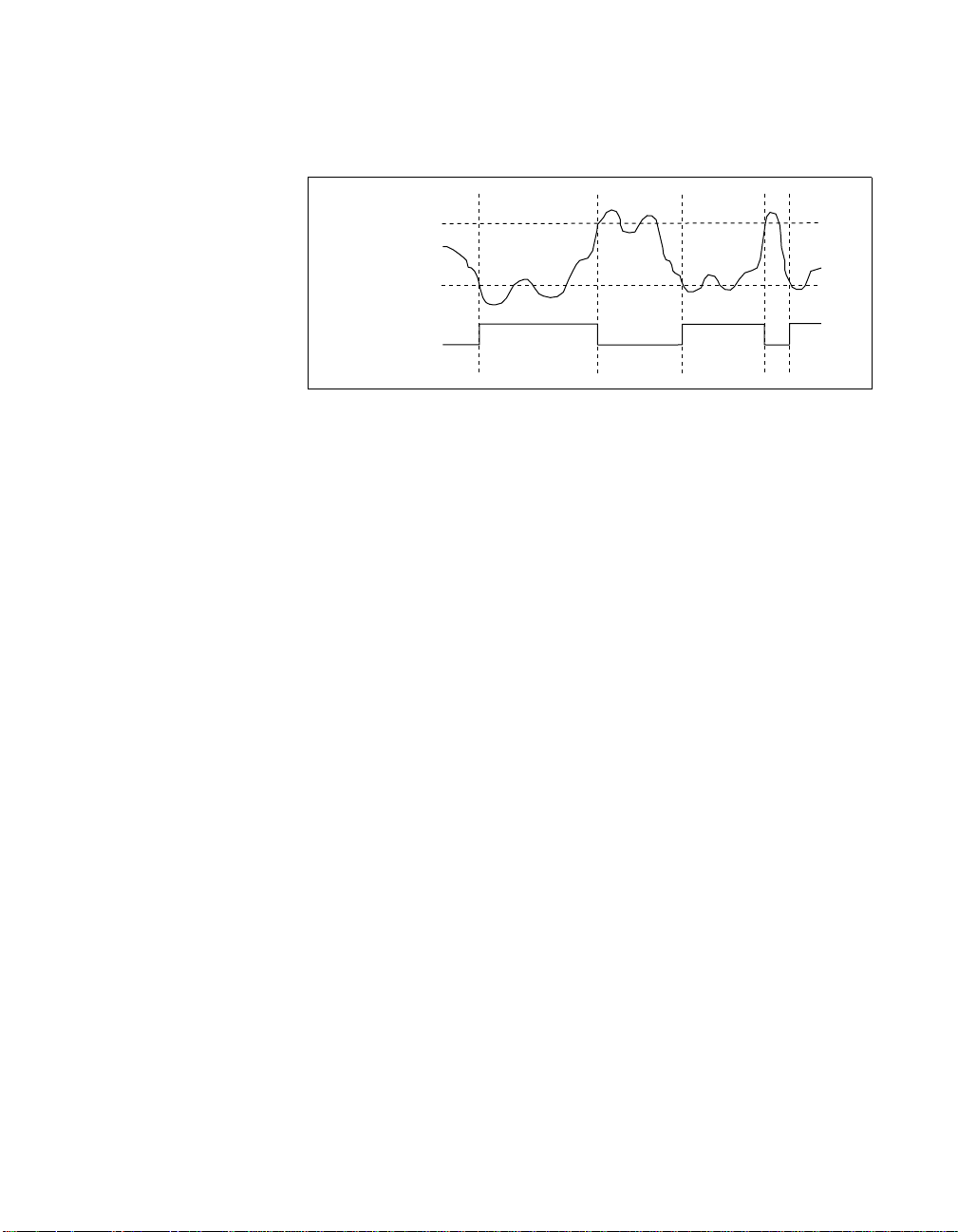
There are five analog level triggering modes available, as shown in
Figures 3-3 throug h 3-7. You can set lowValue and highValue
independently in the software.
In below-low-level triggering mode, shown in Figure 3-3, the trigger is
generated when the signal value is less than lowValue. HighValue is
unused.
lowValue
Trigger
Figure 3-3.
©
National Instruments Corporation 3-7 PCI-4451/4452 User Manual
Below-Low-Level Triggering Mode
Page 25

Chapter 3 Hardware Overview
In above-high-level triggering mode, the trigger is generated when the
signal value is greater than highValue. LowValue i s unu sed .
highValue
Trigger
Figure 3-4.
Above-High-Level Triggering Mode
In inside-region triggering mode, the trigger is generated when the signal
value is between the lowValue and the highValue.
highValue
lowValue
Trigger
Figure 3-5.
Inside-Region Triggering Mode
In high-hysteresi s trigger ing mode, the trigger i s generated when the signal
value is greater than highValue, with the hysteresis specified by lowValue.
highValue
lowValue
Trigger
Figure 3-6.
PCI-4451/4452 User Manual 3-8
High-Hysteresis Triggering Mode
©
National Instruments Corporation
Page 26
Chapter 3 Hardware Overview
In low-hysteresis triggering mode, the trigger is generated when the signal
value is less than lowValue, with the hysteresis specified by highValue.
highValue
lowValue
Trigger
RTSI Triggers
Figure 3-7.
Low-Hysteresis Triggering Mode
Y o u can use digital triggering through the RTSI bus and the external digital
50-pin connector using any one of the eight available programmable
function input (PFI) pi ns. PFI0/TRIG1 (EXT_TRIG) is the pin dedicated to
external digital triggering.
You can trigger the PCI-DSA devices from any other PCI-DSA device or
any National Instruments device that has the RTSI bus feature. You can
connect the devices through the RTSI bus cable. An external digital trigger
can also trigger multiple devices simultaneously by distributing that trigger
through the RTSI bus. You can select the polarity of the external digital
trigger.
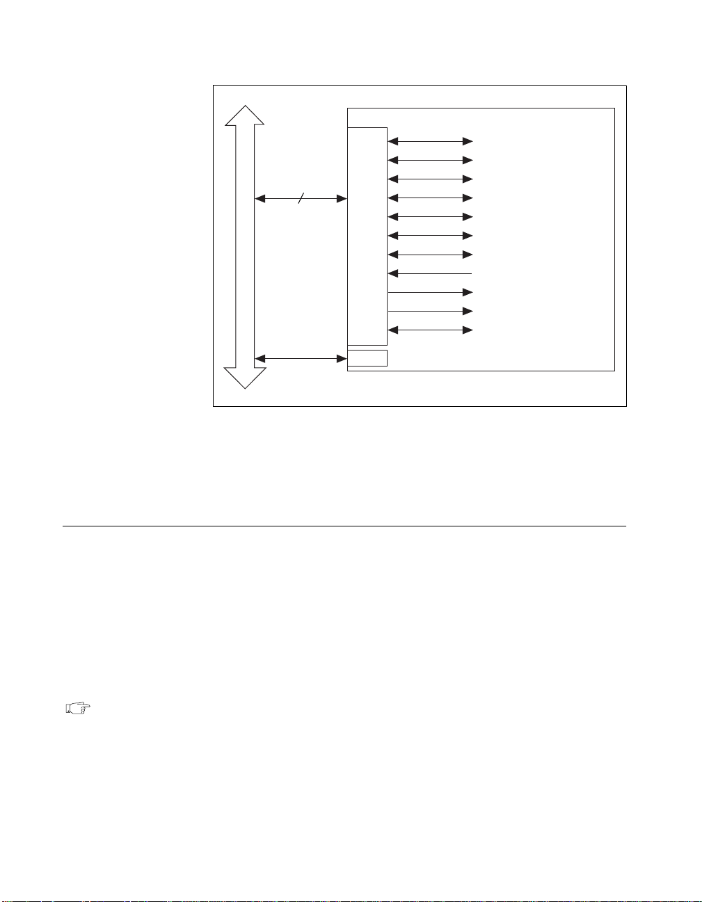
The seven RTSI trigger lines on the RTSI bus provide a very flexible
interconnection scheme for any PCI-4451/4452 device sharing the RTSI
bus. These bidirectional lines can drive any of eight timing signals onto the
RTSI bus and can receive any of these timing signals. This signal
connection scheme is shown in Figure 3-8.
©
National Instruments Corporation 3-9 PCI-4451/4452 User Manual
Page 27
Chapter 3 Hardware Overview
Trigger 7
RTSI Bus Connector
Clock
RTSI Switch
switch
DAQ-STC
TRIG1
TRIG2
CONVERT*
UPDATE*
WFTRIG
GPCTR0_SOURCE
GPCTR0_GATE
GPCTR0_OUT
GPCTR1_SOURCE
GPCTR1_GATE
RTSI_OSC (20 MHz)
Figure 3-8.
RTSI Bus Signal Connection
Refer to the Chapter 4, Signal Connections for a des c ript i on of the signals
shown in Figure 3-8.
Digital I/O
The PCI-4451/4452 devices contain eight lines of digital I/O for
general-purpose use through the 50-pin connector. You can individually
software-configure each line for either input or output.
The hardware up/down control for general-purpose counters 0 and 1 are
connected onboard to DIO6 and DIO7, respectively. Thus, you can use
DIO6 and DIO7 to control the general-purpose counters. The up/down
control signals are input only and do not affect the operation of the DIO
lines.
Note At system power-on and reset, the hardware sets both the PFI and DIO lines to
high impedance. This means that the device circuitry is not actively driving the
output either high or low. F or example, DIO(0) will be in the high impedance state
after power on, and Table 4-4, Digital I/O Signal Summary, shows that there is a
50 kΩ pull-up resistor. This pull-up resistor sets the DIO(0) pin to a logic high
when the output is in a high-impedance state. Take careful consideration of the
power-on state of the system to prevent any damage to external equipment.
PCI-4451/4452 User Manual 3-10
©
National Instruments Corporation
Page 28

Timing Signal Routing
The DAQ-STC provides a flexible interface for connecting timing signals
to other devices or to external circuitry. Your PCI-4451/4452 device uses
the RTSI bus to interconnect timing signals between devices, and uses the
PFI pins on the I/O connector to connect the device to external circuitry.
These connections enable the PCI-4 451/4452 device to both control and be
controlled by other devices and circuits.
There are a total of 13 timing signals internal to the DAQ-STC that you can
control by an external source. You can also control these timing signals by
signals generated internally to the DAQ-STC, and these selections are fully
software configurable. Many of these timing signals are also available as
outputs on the RTSI pins, as indicated in the RTSI Triggers section earlier
in this chapter, and on the PFI pins, as indicated in Chapter 4, Signal
Connections.
Programmable Function Inputs
The 10 PFIs are connected to the signal routing multiplexer for each timing
signal, and software can select one of the PFIs as the external source for a
given timing signal . It is im portant to note that you can use any of th e PFIs
as an input by any of the timing signals and that multiple timing signals can
use the same PFI simultaneously. This flexible routing scheme reduces the
need to change physical connections to the I/O connector for different
applications. You can also individually enable each of the PFI pins to
output a specific internal timing signal. For example, if you need the
GPCTR0_SOURCE signal as an output on the I/O connector, software can
turn on the output driver for the PFI8/GPCTR0_SOURCE pin.
Chapter 3 Hardware Overview
Note
Two o f the 10 PF I pi n s are n ot avai l ab le for general-purpose input on the di git a l
connector . You can confi gure PFI2/C ONVERT * and PFI5 /UPD A TE * as output s
only.
Device and RTSI Clocks
Some PCI-4451/4452 device functions require a frequency timebase to
generate the necessary timing signals for controlling general-purpose
signals at the 50-pin digital I/O connector. You canno t use these signals for
the generating the frequency of sample rates or update rates. Refer to
Selecting Sample/Update Cl ock Freq uency section for information on
sample/update clock generation.
©
National Instruments Corporation 3-11 PCI-4451/4452 User Manual
Page 29

Chapter 3 Hardware Overview
A PCI-4451/4452 device can use either its internal 20 MHz timebase or a
timebase received over the RTSI bus. In addition, if you configure the
device to use the internal timebase, you can pr ogram the de vi ce to dri v e its
internal timebase o ver the RTSI bus to anot her device that you program to
receive this timebase signal. The default configuration at startup is to use
the internal timebase without driving the RTSI bus timebase signal. This
timebase is software-selectable.
Selecting Sample/Update Clock Frequency
The two analog input channels of the PCI-4451 and the four inputs of the
PCI-4452 are simultaneously sampled at any software-programmable rate
from 5.0 kS/s to 204.8 kS/s in 190.7 µS/s increments (worst case). The
devices use direct digital synthesis (DDS) technology so that you can
choose the correct sample rate required for your application. All the input
channels acquire data at the same rate. One input channel cannot acquire
data at a different rate from another input channel.
The two analog output channels of the PCI-4451 are updated
simultaneously at any software programmable rate from 1.25 kS/s to
51.2 kS/s in 47.684 µS/s increments (worst case). The input sample rate
and output update rate on the PCI-4451 are synchronized and deri ved fro m
the same DDS clock. The input and output clocks may differ from each
other by a factor of 2 (1, 2, 4, 8, …, 128) while still maintaining their
synchronization as lon g as the lower bounds for update and sample rate are
maintained. All the output channels update data at the same rate. One
output channel cannot update data at a different rate from another output
channel.
The DDS clock signal and the synchronization start signal are transmitted
to other PCI-DSA devices via the RTSI bus. The PCI-4451/4452 can also
receive these signals to syn chronize the acquisition or wa veform generation
with other devices. In a multidevice system, a master device would drive
the clock and synchronization signal to other slave or receiving devices.
PCI-4451/4452 User Manual 3-12
©
National Instruments Corporation
Page 30

Device Configuration Issues
Selecting a sample rate that is less than two times the frequency of a band
of interest can lead you to believe the board is functioning improperly. By
undersampling the signal, you could receive what appears to be a DC
signal. This situation is due to the sharp antialiasing filters that remove
frequency components above the sampling frequency. If you have a
situation where this occurred, simply increase the sample rate until it meets
the requirements of the Shannon Sampling Theorem. For more information
on the filters and aliasing, refer to Chapter 6, Theory of Analog Opera tio n.
Unlike other converter technologies, delta-sigma converters must be run
continuously and at a minimum clock rate. To operate within guaranteed
specifications, the A/D con verters should operate at a minimum sample rate
of 5.0 kS/s and the D/A converters should operate at a minimum update rate
of 1.25 kS/s. This minimum rate is required to keep the internal circuitry of
the converters running within specifications. You are responsible for
selecting sample and update rates that fall within the specified limits.
Failure to do so could greatly affect the specifications.
Chapter 3 Hardware Overview
©
National Instruments Corporation 3-13 PCI-4451/4452 User Manual
Page 31

Signal Connections
This chapter describes how to make input and output connections to your
PCI-4451/4452 device via th e analog I/O and digital I/ O connectors of t he
device.
The analog I/O connector for the PCI-4451/4452 connects to the
BNC-2140 DSA accessory through the SHC68-C68-A1 shielded cable.
You can access the analog I/O of the PCI-4451/4452 using standard BNC
connectors on the BNC-2140. Y ou can connect the analog I/O sign als to the
shielded cable through a single 68-pin connector.
The digital I/O connector for the PCI-4451/4452 has 50 pins that you can
connect to generic 68-pi n t erm inal blocks through the SHC 50-68 shielded
cable. You can connect the digital I/O signals to the shielded cable through
a single 50-pin connector.
I/O Connectors
Table 4-1 describes the pin assignments for the 68-pin analog I/O
connector. Ta ble 4-3 describes the 50 -pin digital connec tor on the
PCI-4451/4452 devices. A signal description follows the connector
pinouts.
4
Caution
!
©
National Instruments Corporation 4-1 PCI-4451/4452 User Manual
Connections that exceed any of the maximum ratings of input or output signals
on the PCI-4451/4452 devices can damage the PCI-4451/4452 device, the
computer , and associated accessories. Maximum input ratings for each signal are
given in the Protection column of Table 4-2 and 4-4. National Instruments is not
liable for any damages resulting from s uch signal connections.
Page 32

Chapter 4 Signal Connections
Analog I/O Connector Signal Descriptions
Figure 4-1 shows the analog pin connections for the PCI-4451/4452.
-ACH0
NC
-ACH1
NC
ACH2-
NC
-ACH3
NC
NC
NC
NC
NC
NC
NC
NC
NC
NC
NC
NC
NC
NC
NC
NC
NC
-DAC0 OUT
NC
-DAC1 OUT
NC
NC
NC
NC
NC
+5 V
GND
135
236
337
438
539
640
741
842
943
10 44
11 45
12 46
13 47
14 48
15 49
16 50
17 51
18 52
19 53
20 54
21 55
22 56
23 57
24 58
25 59
26 60
27 61
28 62
29 63
30 64
31 65
32 66
33 67
34 68
+ACH0
GND
+ACH1
GND
+ACH2
GND
+ACH3
GND
NC
NC
NC
NC
NC
NC
NC
NC
NC
NC
NC
NC
NC
NC
NC
NC
+DAC0 OUT
GND
+DAC1 OUT
GND
NC
NC
NC
NC
+5 V
GND
Figure 4-1.
PCI-4451/4452 User Manual 4-2
Analog Pin Connections
©
National Instruments Corporation
Page 33

Chapter 4 Signal Connections
Table 4-1.
Signal Name Reference Direction Description
+ACH<0..3> AIGND Input +Analog Input Channel 0 throu gh 3—The PCI-4451 uses
−ACH<0..3>
AIGND Input
Analog I/O Connector Pin Assignment
+ACH<0..1> and the PCI-4452 uses +ACH<0..3>.
−Analog Input Channel 0 through 3—The PCI-4451 uses
−ACH<0..1> and the PCI-445 2 uses −ACH<0..3>.
AIGND — — Ana log Input Ground—These pins are the reference point for
single-ended measure m ents in SE configuration and t he bias
current return point for di fferential measurement s . Al l three
ground references—AIGND, AOGND, and DGND—are
connected together on your PCI-4451/4452 device, but each
serves a separate purpose.
+DAC0OUT
−DAC0OUT
+DAC1OUT
−DAC1OUT
AOGND — — Analog Output Ground—The anal og output voltages are
+5 V DGND Output +5 VDC Source—These pins are fused for up to 0. 5 A and
DGND — — Dig it al Ground—This pin supplies the reference for the +5
−DAC0OUT
+DAC0OUT Output
−DAC1OUT
+DAC1OUT Output
Output +Analog Output Channel 0—T hi s pin supplies the analog
non-inverting output channel 0. This pin is available only on
the PCI-4451.
−Analog Output Channel 0—This pin supplies the an al og
inverting output channel 0. This pin is available only on the
PCI-4451.
Output +Analog Output Channel 1—T hi s pin supplies the analog
non-inverting output channel 1. This pin is only available on
the PCI-4451.
−Analog Output Channel 1—This pin supplies the an al og
inverting output channel 1. This pin is only available on the
PCI-4451.
ultimately refere nc ed to this node. All three ground
references—AIGND, AOGND, and DGND—are connected
together on your PCI-4451/4 452 device, but each serves a
separate purpose.
supply power to the DSA signal conditioning accessories.
The fuse is s elf resetting.
VDC supply. All three ground references—AIGND, AOGND,
and DGND—are connected together on your PCI-4451/4452
device, but each serves a sep ara te purpose.
©
National Instruments Corporation 4-3 PCI-4451/4452 User Manual
Page 34

Chapter 4 Signal Connections
Table 4-2.
Signal
Signal Name
+ACH<0..3>
ACH<0..3>
−
AIGND
+DAC0OUT
DAC0OUT
−
+DAC1OUT
DAC1OUT
−
AOGND
DGND
+5 V
AI = Analog Input DIO = Digital Input/Outpu t
AO = Analog Output DO = Digital Output
†
±400 V/±400 V guarantee d by de sign, but not tested or certi fied to operate beyond ± 42. 4 V
Type and
Direction
AI
AI
AI — — — — — —
AO
AO
AO
AO
AO — — — — — —
DIO — — — — — —
DO
Impedance
Input/
Output
1 MΩ
in parallel
with
50 pF to
AIGND
1 MΩ
in parallel
with
50 pF to
AIGND
22 Ω to
DAC0OUT,
−
4.55 kΩ to
AOGND
22 Ω to
+DAC0OUT,
4.55 kΩ to
AOGND
22 Ω to
DAC1OUT,
−
4.55 kΩ to
AOGND
22 Ω to
+DAC1OUT,
4.55 kΩ to
AOGND
0.7 Ω Short-circuit to
Analog I/O Signal Summary
Protection
(V olts)
On/Off
±42.4 V/±42.4 V
±42.4 V/±42.4 V
Short-circuit to
DAC0OUT,
−
ground
Short-circuit to
+DAC0OUT,
ground
Short-circuit to
DAC1OUT,
−
ground
Short-circuit to
+DAC1OUT,
ground
ground
Source
(mA at V)
†
— — —
†
— — —
16.7 mA at
10 V
16.7 mA at
10 V
16.7 mA at
10 V
16.7 mA at
10 V
0.5A
Sink
(mA at
V)
— — —
— — —
— — —
— — —
— — —
Rise
Time
(ns)
Bias
±100 pA
±100 pA
PCI-4451/4452 User Manual 4-4
©
National Instruments Corporation
Page 35

Digital I/O Connector Signal Descriptions
Figure 4-2 shows the digital pin connections for the PCI-4451/4452.
Chapter 4 Signal Connections
FREQ_OUT
GPCTR0_OUT
PFI8/GPCTR0_SOURCE
PFI6/WFTRIG
PFI7
GPCTR1_OUT
PFI3/GPCTR1_SOURCE
PFI1/TRIG2 (PRETRIG)
CONVERT*
DIO(7)
DIO(6)
DIO(0)
DIO(2)
DIO(4)
DIO(3)
+5 V
+5 V
+5 V
N/C
N/C
N/C
N/C
N/C
N/C
N/C
126
227
328
429
530
631
732
833
934
10 35
11 36
12 37
13 38
14 39
15 40
16 41
17 42
18 43
19 44
20 45
21 46
22 47
23 48
24 49
25 50
DGND
PFI9/GPCTR0_GATE
DGND
UPDATE*
DGND
PFI4/GPCTR1_GATE
DGND
PFI0/TRIG1(EXT_TRIG)
DGND
RESERVED1
DGND
DIO(1)
DGND
EXTSTROBE*
DGND
DIO(5)
N/C
+5 V
DGND
N/C
DGND
N/C
DGND
N/C
DGND
Figure 4-2.
Digital Pin Connections
Refer to Appendix B, Pin Connections , for the digital pin connections of
the 68-pin connector.
©
National Instruments Corporation 4-5 PCI-4451/4452 User Manual
Page 36

Chapter 4 Signal Connections
Table 4-3.
Signal Name Reference Direction De scription
DIO<0..7> DGND Input or
DGND — — Digital Ground—This pin supplies the reference for the digital
+5 V DGND Output +5 VDC Source—These pins are fused for up to 1 A of +5 V
RESERVED1 DGND Output RESERVED—This pin is reserved. This signal is always high.
EXTSTROBE* DGND Output Externa l Strobe—This signal can be toggled under software
PFI0/TRIG1 (EXT_TRIG) DGND Input
PFI1/TRIG2 (PRETRIG) DGND Input
CONVERT* DGND Output A high-to-low edge on CONVERT* indicates that an A/D
PFI3/GPCTR1_SOURCE DGND Input
Digital I/O Connector Pin Assignment
Output
Output
Output
Digital I/O channels 0 through 7—Channels 6 and 7 can
control the up/down signal of general-purpose counters 0
and 1, respectivel y.
signals at the I/O connector as we ll as the +5 VDC supply.
supply. The fuse is self-resetting.
control to latch sign al s or trigger events on external devices.
TRIG1—As an input, this is a source for the data acquisition
trigger.
As an output, this signa l can drive external applications to
indicate that a trigger on the device has occurred. TRIG1 is the
start acquisi tion signal.
In LabVIEW, referred to as AI Start Trigger for both input and
output.
PFI1/TRIG2 (PRETRIG)—As an in put , this is one of the
PFIs.
As an output, this is the TRIG2 sig nal . In pre tri gger
applications, a low-to-high transition indicates the initiation of
the posttrigger conversi ons. TR IG2 is not used in posttrigger
applications.
In LabVIEW, referred to as AI Stop Trigger for both input and
output.
conversion is oc curring.
In LabVIEW, referred to as AI Convert.
PFI3/Counter 1 Source— As an input, this is one of the PFIs.
Output
PFI4/GPCTR1_GATE DGND Input
Output
UPDATE* DGND Output A high-to-low edge on UPDATE* indicates that a D/A
PCI-4451/4452 User Manual 4-6
As an output, this is the GPCTR1_SOURCE signal. This signal
reflects the actua l source connected to th e general-purpose
counter 1.
PFI4/Counter 1 G ate—As an input , th is is one of the PFIs.
As an output, this is the GPCTR1_GATE signal. This signal
reflects the actual gate signal connected to the general-purpose
counter 1.
conversion is oc curring.
In LabVIEW, referred to as AO Upda te.
©
National Instruments Corporation
Page 37

Chapter 4 Signal Connections
Table 4-3.
Signal Name Reference Direction De scription
GPCTR1_OUT DGND Out put General-Purpose Counter 1 Output
PFI6/WFTRIG DGND Input
PFI7 DGND Input PFI7—This is one of the PFIs.
PFI8/GPCTR0_SOURCE DGND Input
PFI9/GPCTR0_GATE DGND Input
GPCTR0_OUT DGND Out put General-Purpose Counter 0 Output
FREQ_OUT DGND Output Frequency Output—This output is from the frequency
Digital I/O Connector Pin Assignment (Continued)
PFI6/Waveform Trigger—As an input, this is one of the PFIs.
Output
Output
Output
As an output, this is the WFTRIG signal. In timed analog
output sequences, a low-to-high tran s ition indicates the
initiation of the wave form generation.
In LabVIEW, referred to as AO Start Trigger for both input
and output.
PFI8/Counter 0 Source—As an input, this is one of the
PFIs.
As an output, this is the GPCTR0_SOURCE signal. This signal
reflects the actua l source connected to th e general-purpose
counter 0.
PFI9/Counter 0 Gate—As a n input, this is one of the PFIs.
As an output, this is the GPCTR0_GATE signal. This signal
reflects the actual gate signal connected to the general-purpose
counter 0.
generator output.
©
National Instruments Corporation 4-7 PCI-4451/4452 User Manual
Page 38

Chapter 4 Signal Connections
Table 4-4.
Signal
Signal Name
DGND
+5 V
DIO<0..7>
RESERVED1
EXTSTROBE*
PFI0/TRIG1 (EXT_TRIG)
PFI1/TRIG2 (PRETRIG)
CONVERT*
PFI3/GPCTR1_SOURCE
PFI4/GPCTR1_GATE
GPCTR1_OUT
UPDATE*
PFI6/WFTRIG
PFI7
PFI8/GPCTR0_SOURCE
PFI9/GPCTR0_GATE
GPCTR0_OUT
FREQ_OUT
DIO = Digital Input/Output pu = pullup
DO = Digital Output DI = Digital Input
Note: The tolerance on the 50 kΩ pullup and pulldown resistors is very large. Actual value may range between 17 and 100 kΩ.
Type and
Direction
DIO —
DIO 0.15 Ω
DIO —
DO —
DO —
DIO —
DIO —
DO —
DIO —
DIO —
DO —
DO —
DIO —
DI —
DIO —
DIO —
DO —
DO —
Digital I/O Signal Summary
Impedance
Input/
Output
Protection
(V olts)
On/Off
— — —
Short-circuit
to ground
Vcc +0.5 13 at
— — —
— 3.5 at
Vcc +0.5 3.5 at
Vcc +0.5 3.5 at
— 3.5 at
Vcc +0.5 3.5 at
Vcc +0.5 3.5 at
— 3.5 at
— 3.5 at
Vcc +0.5 3.5 at
Vcc +0.5 — —
Vcc +0.5 3.5 at
Vcc +0.5 3.5 at
— 3.5 at
— 3.5 at
Source
(mA at V)
1A —
24 at 0.4
(Vcc
0.4)
−
5 at 0.4
(Vcc
0.4)
−
5 at 0.4
(Vcc
0.4)
−
5 at 0.4
(Vcc
0.4)
−
5 at 0.4
(Vcc
0.4)
−
5 at 0.4
(Vcc
0.4)
−
5 at 0.4
(Vcc
0.4)
−
5 at 0.4
(Vcc
0.4)
−
5 at 0.4
(Vcc
0.4)
−
5 at 0.4
(Vcc -0.4)
5 at 0.4
(Vcc
0.4)
−
5 at 0.4
(Vcc
0.4)
−
5 at 0.4
(Vcc
0.4)
−
5 at 0.4
(Vcc
0.4)
−
Sink
(mA at
V)
Rise
Time
(ns)
—
—
1.1
—
1.5
1.5
1.5
1.5
1.5
1.5
1.5
1.5
1.5
—
1.5
1.5
1.5
1.5
Bias
—
—
50 kΩ pu
50 kΩ pu
50 kΩ pu
50 kΩ pu
50 kΩ pu
50 kΩ pu
50 kΩ pu
50 kΩ pu
50 kΩ pu
50 kΩ pu
50 kΩ pu
50 kΩ pu
50 kΩ pu
50 kΩ pu
50 kΩ pu
50 kΩ pu
PCI-4451/4452 User Manual 4-8
©
National Instruments Corporation
Page 39

Analog Input Signal Connections
The analog input signals for the PCI-4451 /4452 d evices are +ACH<0..3>,
−ACH<0..3>, and AIGND. The +
analog input channels of your PCI-4451, and ±ACH<0..3> are tied to the
four analog input channels of your PCI-4452 device.
Chapter 4 Signal Connections
ACH<0..1> signals are tied to the two
!
+ACH
-ACH
AIGND
Caution
x
Calibration
Multiplexer
x
Exceeding the differential and common-mode input ranges distorts your input
signals.
AIGND is an analog input common signal that connects directly to the
ground system on the PCI -4451/44 52 de vices. You can use t his sign al for a
general analog ground tie point to your PCI-4451/4452 de vice if necessary ,
but connecting AIGND to other earth-connected grounds is not
recommended. AIGND is not directly available if you are using a
BNC-2140 accessory.
Figure 4-3 shows a diagram of your PCI-4451/4452 device analog input
stage.
20 dB
Attenuator
AIGND
Differential
Amplifier
+
–
Gain = 0 dB
Gain = 10 dB
Gain = 20 dB
Gain = 30 dB
Gain = 40 dB
Gain = 50 dB
Gain = 60 dB
Analog
Lowpass
Filter
A/D
Converter
0.047 F
1 GΩ
1 GΩ
0.047 F
= 3.4 Hz
f
c
DC/AC
Coupling
900 kΩ
100 kΩ
100 kΩ
900 kΩ
Gain = 0 dB
Gain = -20 dB
Figure 4-3.
Analog Input Stage
The analog input stage applies gain and common-mode voltage rejection
and presents high input impedance to the analog input signals connected to
your PCI-4451/4452 de vice. Si gnals are rou ted di rectly to t he positive and
negative inputs of the analog input stage on the device. The analog input
stage converts two input signals to a signal that is the difference between
the two input signals multiplied by the gain setting of the amplifier. The
©
National Instruments Corporation 4-9 PCI-4451/4452 User Manual
Page 40

Chapter 4 Signal Connections
amplifier output voltage is referenced to the ground for the device. Your
PCI-4451/4452 device A/D converter (ADC) measu res t his o ut put voltage
when it performs A/D conversi ons.
Connection of analo g input s ignals to your PCI -4451/4 452 de vice dep ends
on the configuration of the input signal sources. For most signals, you use
a DIFF configuration and simply connect the signal to +ACHx (where x is
the PCI-4451/4452 channel) and the signal ground (or signal minus, as
appropriate) to −ACHx. However, if a signal has a high output impedance
(greater than 1 kΩ) and is floating, you may find it useful to use an SE
configuration and tether the signal minus to AIGND to reduce
common-mode interference. You can make the DIFF and SE connections
through the BNC-2140 accessory.
Types of Signal Sources
When configuring the input ch annels and mak i ng s ignal co nnecti on s, f irst
determine whether the signal sources are floating or ground-referenced.
The following sections describe these two types of signals.
Floating Signal Sources
A floating signal sou rce does not connect in any way to the building ground
system but instead has an isolated ground-reference point. Some examples
of floating signal sources are outputs of transformers, thermocouples,
battery-powered devices, o ptical i solator ou tputs, and is olation am plifi ers.
An instrument or device that has an isolat ed output is a floating signal
source.
Ground-Referenced Signal Sources
A ground-referenced signal source connects in some way to the building
system ground and is, therefore, already connected to a common ground
point with respect to the PCI-4451/4452 device, assuming that you plug the
computer into the same power s ystem. Noni solat ed out puts of i nstrumen ts
and devices that plug into the building power system fall into this category.
The difference in ground potential between two instruments connected to
the same building po wer system is typicall y between 1 and 100 mV but can
be much higher if power distribution circuits are not properly connected.
For this reason, National Instruments does not recommend connecting
AIGND to the source signal ground system, since the difference between
the grounds can induce currents in the PCI-4451/4452 ground system.
PCI-4451/4452 User Manual 4-10
©
National Instruments Corporation
Page 41

Analog Output Signal Connections
The analog output signals for the PCI-4451 device are +DAC0OUT,
−DAC0OUT, +DAC1OUT, -DAC1OUT, and AOGND. +DAC0OUT and
−DAC0OUT are the plus and minus voltage output signals for analog
output channel 0. +DAC1OUT and −DAC1OUT are the plus and minus
voltage output signal, for analog output channel 1.
AOGND is a ground -reference signal for b oth analog output chann els. It is
connected directly to the ground system on the PCI-4451 device. You can
use this signal for a general analog ground tie point to your PCI-4451
device if necessary, but connecting AOGND to other earth-connected
grounds is not recommended. AOGND is not directly available if you are
using the BNC-2140 accessory.
The PCI-4451 has two analog output channels, either of which is illustrated
in Figure 4-4.
Chapter 4 Signal Connections
D/A
Converter
Gain = 0 dB
Gain = -20 dB
Gain = -40 dB
Gain = -∞ dB
100 kΩ
+DACxOUT
10 kΩ
-DAC
100 kΩ
AOGND
x
OUT
Attenuator
Balanced
Differential
Driver
Figure 4-4.
11 Ω
11 Ω
Analog Output Channel Block Diagram
The analog output stage is differential and balanced. Each output signal
consists of a plus connection, a minus connection, and a ground (A OGND)
connection. The actual output signal is the dif ference between the plus and
minus connections. The pair is balanced, meaning that, if the impedances
from each of the pair to AOGND is the same (or inf i nite), then the vo ltage
at the plus and minus terminals are equal but opposite, so that their
difference is the desired signal and their sum (or average) is zero. If
impedances from each of the pair to AOGND is not the same, the
connection is unbalanced, but the difference between the plus and minus
©
National Instruments Corporation 4-11 PCI-4451/4452 User Manual
Page 42

Chapter 4 Signal Connections
terminals is still equal to the desired signal. If the minus side is grounded,
the plus voltage is equal to the signal. Conversely, if the plu s sid e is
grounded, the minus voltage is equal to the negative of the signal. In all
cases, the difference is equal to the signal.
Connection of analog output signals from your PCI-4451 device depends
on the configuration of the devices receiving the signals. For most sig nals,
you use a DIFF configuration and simply connect +D A CxOUT (wher e x is
the PCI-4451 channel) to the signal and −DACxOUT to the signal ground
(or signal minus, as appropriate). When driving some floating devices,
however , you may sometimes find it helpful to use the SE configuration and
connect the floating ground system of the device to AOGND to reduce
common-mode noise coupled from an interfering source to the de v ice.You
can make DIFF and SE connections through the BNC-2140 accessory.
Analog Power Connections
Two pins on the analog I/O connector supply +5 V from the computer
power supply via a self-resetting fuse. The fuse will reset automatically
within a few seconds after the overcurrent condition is removed. These pins
are referenced to DGND and you can use them to power external analog
accessories like the BNC-2140.
• Power rating +4.65 to +5.25 VDC at 0.5 A
Caution
!
Do not under any circumstances connect these +5 V power pins directly to analog
ground, digital ground, or to any other voltage source on the PCI-4451/4452
device or any other device. Doing so can damage the PCI-4451/4452 device and
the computer. National Instruments is not liable for damages resulting from such
a connection.
Digital I/O Signal Connections
The digital I/O signals are DIO<0..7> and DGND. DIO<0..7> are the
signals making up the DIO por t. DGND is the ground-reference signal fo r
the DIO port. You can p rogram all lines in dividually to be inputs or o utputs.
PCI-4451/4452 User Manual 4-12
©
National Instruments Corporation
Page 43

LED
Chapter 4 Signal Connections
Figure 4-5 shows signal connections for three typical digital I/O
applications.
+5 V
DIO<4..7>
+5 V
Switch
I/O Connector
TTL Signal
Figure 4-5.
DGND
Digital I/O Connections
DIO<0..3>
Figure 4-5 shows DIO<0..3> configured for digital input and DIO<4..7>
configured for digital output. Digital input applications include receiving
TTL signals and sensing external device states such as the state of the
switch shown in Figure 4-5. Digital output applications include s e nding
TTL signals and driving external devices such as the LED shown in
Figure 4-5.
©
National Instruments Corporation 4-13 PCI-4451/4452 User Manual
Page 44

Chapter 4 Signal Connections
Digital Power Connections
Four pins on the digital I/O connector supply +5 V from the computer
power supply via a self-resetting fuse. The fuse will reset automatically
within a few seconds after the overcurrent condition is removed. These pins
are referenced to DGND and you can use them to power external digital
circuitry.
• Power rating +4.65 to +5.25 VDC at 1 A
Caution
!
Do not under any circumstances connect these +5 V power pins directly to analog
ground, digital ground, or to any other voltage source on the PCI-4451/4452
device or any other device. Doing so can damage the PCI-4451/4452 device and
the computer. National Instruments is not liable for damages resulting from such
a connection.
Timing Connections
All external control over the timing o f your PCI-4451/44 52 device is routed
through the 10 programmable function inputs labeled PFI0 through PFI9
(excluding PFI2 and PF I5). These signals are explained in detail in the next
section, Programmable Function Input Connections. Most of these PFIs
are bidirectional. As outputs they are not programmable and reflect the
state of acquisition, waveform generation, and general-purpose timing
signals. As inputs, the PFI signals are programmable and can control any
acquisition, waveform generation, and general-purpose timing signals.
The acquisition signals are explained in the Acquisition Timing
Connections section later in this chapter. The wa veform generation signals
are explained in the Waveform Generation Timing Connections section
later in this chapter. The general-purpose timing signals are explained in the
General-Purpose Timing Signal Connections section later in this chapter.
All digital timing connections are referenced to DGND.
Programmable Function Input Connections
You can individually enable each of the PFI pins to output a specific
internal timing signal. For example, if you need the GPCTR1_SOURCE
signal as an output on the I/O connector, software can turn on the output
driver for the PFI3/GPCTR1_SOURCE pin.
Caution
Be careful not to drive a PFI signal externally when it is configured as an output.
!
PCI-4451/4452 User Manual 4-14
©
National Instruments Corporation
Page 45

As an input, you can individually configure each PFI for edge or level
detection and for polarity selection as well. You can use the polarity
selection for any of the timing signals, but the edge or level detection
depends upon the particular timing signal being controlled. The detection
requirements for each timing signal are listed within the section that
discusses that individual signal.
In edge-detection mode, the minimum pulse width required is 10 ns. This
applies for both rising-edge and falling-edge polarity settings. There is no
maximum pulse-width requirement in edge-detect mode.
In level-detection mode, there are no minimum or maximum pulse-width
requirements imposed by the PFIs themselves, but there can be limits
imposed by the particular timing signal being controlled. These
requirements are listed later in this chapter.
Acquisition Timing Connections
The acquisition timing signals are PFI0/TRIG1, PFI1/TRIG2,
CONVERT*, and EXTSTROBE*.
Posttriggered data acquis ition allo ws you to vie w only data that is acquired
after a trigger event is received. A typical posttriggered acquisition
sequence is shown in Figure 4-6.
Chapter 4 Signal Connections
TRIG1
CONVERT*
Scan Counter
Figure 4-6.
©
National Instruments Corporation 4-15 PCI-4451/4452 User Manual
Typical Posttriggered Acquisition
13042
Page 46

Chapter 4 Signal Connections
TRIG1
Pretriggered data acquisition allows you to view data that is acquired b efore
the trigger of interest in addition to data acquired after the trigger.
Figure 4-7 shows a typical pretriggered acquisition sequence. The
description for each signal shown in these figures is included later in this
chapter.
TRIG2
CONVERT*
Sample Counter
Don't Care
01231 0222
Figure 4-7.
Typical Pretriggered Acquisition
Don't Care
PFI1
PFI0/TRIG1 (EXT_TRIG) Signal
Any PFI pin can externally input the PFI0/TRIG1 (EXT_TRIG) signal,
which is available as an output on the PFI0/TR IG 1 (EXT_TR I G) pin .
Refer to Figures 4-6 and 4-7 for the relationship of PFI0/TRIG1 to the
acquisition sequence.
As an input, the PFI0/TRIG1 signal is configured in the edge-detection
mode. You can select any PFI pin as the source for PFI0/TRIG1 and
configure the polarity selection for either rising or falling edge. The
selected edge of the PFI0/TRIG1 signal starts the data acqu isition sequence
for both posttriggered and pretriggered acquisitions. The PCI-4451/4452
supports analog level triggering on the PFI0/TRIG1 p in. See Chapter 3,
Hardware Overview, for more information on analog level triggering.
As an output, the PFI0/TRIG1 signal reflects the action that initiates an
acquisition sequence. This is true even if the acquisition is externally
triggered by another PFI signal. The output is an active high pulse with a
pulse width of 50 to 100 ns. This ou tput is set to tri-state at startup.
The device also uses the PFI0/TRIG1 signal to initiate pretriggered
acquisition operations. In most pretriggered applications, the PFI0/TRIG1
signal is generated by a software trigger. Refer to the PFI1/TRIG2 signal
description for a complete description of the use of PFI0/TRIG1 and
PFI1/TRIG2 in a pretriggered acquisition operation.
PCI-4451/4452 User Manual 4-16
©
National Instruments Corporation
Page 47

Chapter 4 Signal Connections
PFI1/TRIG2 (PRETRIG) Signal
Any PFI pin can externally input the PFI/1TRIG2 (PRETRIG) signa l,
which is available as an output on the PFI1/TR IG 2 (PR E TRIG) pin.
Refer to Figure 4-7 for the relationship of PFI1/TRIG2 to the acquisition
sequence.
As an input, the P F I1/ TR IG2 si gn al is co nfigured in edge-detection mode.
Y o u can select any PFI pin as the source for PFI1/TRIG2 and conf igure the
polarity selection for either rising or falling edge. The selected edge of the
PFI1/TRIG2 signal initiates the posttriggered phase of a pretriggered
acquisition sequence. In pretriggered mode, the PFI0/TRIG1 signal
initiates the data acquisition. The scan counter indicates the minimum
number of scans before PFI1/TRIG2 is recognized. After the scan counter
decrements to zero, it is loaded with the number of posttrigger scans to
acquire while the acquisition continues. The device ignores the
PFI1/TRIG2 signal if it is asserted prior to the scan counter decrementing
to zero. After the selected edge of PFI1/TRIG2 is received, the device
acquires a fixed number of scans and the acquisition stops. After
PFI1/TRIG2 is received, any additional PFI1/TRIG2 signals are ignored
until the acquisition is restarted. This mode acquires data both before and
after receiving PFI1/TRIG2.
As an output, the PFI1/TRIG2 signal reflects the posttrigger in a
pretriggered acquisition sequence. This is true even if the acquisition is
externally triggered by another PFI signal. The PFI1/TRIG2 signal is not
used in posttriggered data acquisition. The output is an active high pulse
with a pulse width of 50 to 100 ns. This output is set to tri-state at startup.
CONVERT* Signal
The CONVERT* signal is only available as an output on the CONVERT*
pin. The CONVERT* signal reflects the end of delta-sigma conversion on
the ADC. The output is an active-low pulse with a pulse width of 70 to 100
ns. This output is set to tri-state at startup.
©
National Instruments Corporation 4-17 PCI-4451/4452 User Manual
Page 48

Chapter 4 Signal Connections
EXTSTROBE* Signal
EXTSTROBE* is an output-only signal that generates either a single pulse
or a sequence of eight pulses in the hardware-strobe mode. An external
device can use this signal to latch signals or to trigger events. In
single-pulse mode, software controls the level of the EXTSTRO BE*
signal. A 10 µs and a 1.2 µs clock is available for generating a sequence
of eight pulses in hardware-strobe mode. Figure 4-8 shows the timing for
hardware-strobe mode EXTSTROBE* signal.
V
OH
V
OL
t
t
w
w
t
= 600 ns or 5 µs
w
Figure 4-8.
EXTSTROBE* Signal Timing
Waveform Generation Timing Connections
The waveform generation timing signals are WFTRIG and UPDATE*.
WFTRIG Signal
Any PFI pin can externally input the WFTRIG signal, which is available as
an output on the PFI6/WFTRIG pin.
As an input, the WFTRIG signal is configured in the edg e-detection mode.
You can select any PFI pin as the source for WFTRIG and configure the
polarity selection for either rising or falling edge. The selected edge of the
WFTRIG signal starts the waveform generation for the DACs.
As an output, the WFTRIG signal reflects the trigge r that in itiates
waveform generation. This is true even if the waveform generation is
externally triggered by another PFI signal. The output is an active high
pulse with a pulse width of 50 to 100 ns. This output is set to tri-state at
startup.
UPDATE* Signal
The UPDATE* signal is only availabl e as an o utput on t he UPDATE* pin .
The UPDATE* signal reflects the end of a delta-sigma conversion on the
DACs. The output is an active-low pulse with a pulse width of 70 to 100 ns.
This output is set to tri-state at startup.
PCI-4451/4452 User Manual 4-18
©
National Instruments Corporation
Page 49

General-Purpose Timing Signal Connections
The general-purpose timing signals are GPCTR0_SOURCE,
GPCTR0_GATE, GPCTR0_OUT, GPCTR0_UP_DOWN,
GPCTR1_SOURCE, GPCTR1_GATE, GPCTR1_OUT,
GPCTR1_UP_DOWN, and FREQ_OUT.
GPCTR0_SOURCE Signal
Any PFI pin can externally input the GPCTR0_SOURCE signal, which
is available as an output on the PFI8/GPCTR0_SOURCE pin.
As an input, the GPCTR0_SOURCE signal is configured in the
edge-detection mode. You can select any PFI pin as the source for
GPCTR0_SOURCE and configure the polarity selection for either rising
or falling edge.
As an output, the GPCTR0_SOURCE signal reflects the actual clock
connected to general-purpose counter 0. This is true even if another PFI
signal is externally inputting the source clock. This output is set to tri-state
at startup.
Figure 4-9 shows the timing requirements for the GPCTR0_SOURCE
signal.
Chapter 4 Signal Connections
t
p
t
Figure 4-9.
t
w
w
t
= 50 ns minimum
p
t
= 23 ns minimum
w
GPCTR0_SOURCE Signal Timing
The maximum allowed frequen cy is 20 MHz, with a minimum pulse width
of 23 ns high or low. There is no minimum frequency limitation.
The 20 MHz or 100 kHz timebase normally generates the
GPCTR0_SOURCE signal unless you select some external source.
©
National Instruments Corporation 4-19 PCI-4451/4452 User Manual
Page 50

Chapter 4 Signal Connections
GPCTR0_GATE Signal
Any PFI pin can externally input the GPCTR0_GATE signal, which is
available as an output on the PFI9/GPCTR0_GATE pin.
As an input, the GPCTR0_GATE signal is configured in the edge-detection
mode. You can select any PFI pin as the source for GPCTR0_GATE and
configure the polarity selection for either rising or falling edge. Y ou can use
the gate signal in a variety of different applications to perform actions such
as starting and stopping the counter, generating interrupts, saving the
counter contents, and so on.
As an output, the GPCTR0_GATE signal reflects the actual gate signal
connected to general-purpose counter 0. This is true even if the gate is being
externally generated by another PFI signal. This output is set to tri-state at
startup.
GPCTR0_OUT Signal
This signal is available only as an output on the GPCTR0_OUT pin. The
GPCTR0_OUT signal reflects the terminal count (TC) of general-p urp ose
counter 0. You have two software-s electable ou tput o ption s—pulse o n TC
and toggle output po larity on TC. The out put polarity is software selectable
for both options. This output is set to tri-state at startup. Figure 4-10 shows
the timing of the GPCTR0_OUT signal.
GPCTR0_SOURCE
GPCTR0_OUT
(Pulse on TC)
GPCTR0_OUT
(Toggle output on TC)
Figure 4-10.
GPCTR0_UP_DOWN Signal
This signal can be externally input on the DIO6 pin and is no t available as
an output on the I/O connector. The general-purpose counter 0 will count
down when this pin is at a logic low and count u p when it is at a logic high .
You can disable this input so that software can control the up-down
functionality and leave the DIO6 pin free for general use.
PCI-4451/4452 User Manual 4-20
TC
GPCTR0_OUT Signal Timing
©
National Instruments Corporation
Page 51

Chapter 4 Signal Connections
GPCTR1_SOURCE Signal
Any PFI pin can externally input the GPC TR1_SOURCE signal, which is
available as an output on the PFI3/GPCTR1_SOURCE pin.
As an input, the GPCTR1_S OURCE signal is conf igured in edge-detect ion
mode. Y ou can select an y PFI pin as the source for GPCTR1_SOURCE and
configure the polarity selection for either rising or falling edge.
As an output, the GPCTR1_SOURCE monitors the actual clock connected
to general-purpose counter 1. This is true even if the source clock is
externally generated by another PFI signal. This output is set to tri-state at
startup.
Figure 4-11 shows the ti ming requirements for the GP CTR1_SOURCE
signal.
t
p
t
Figure 4-11.
t
w
w
t
= 50 ns minimum
p
t
= 23 ns minimum
w
GPCTR1_SOURCE Signal Timing
The maximum allowed frequen cy is 20 MHz, with a minimum pulse width
of 23 ns high or low. There is no minimum frequency limitation.
The 20 MHz or 100 kHz timebase normally generates the
GPCTR1_SOURCE unless you select some external source.
GPCTR1_GATE Signal
Any PFI pin can externally input the GPCTR1_GATE signal, which is
available as an output on the PFI4/GPCTR1_GATE pin.
As an input, the GPCTR1_GATE signal is configured in edge-detection
mode. You can select any PFI pin as the source for GPCTR1_GATE and
configure the polarity selection for either rising or falling edge. Y ou can use
the gate signal in a variety of different applications to perform such actions
as starting and stopping the counter, generating interrupts, saving the
counter contents, and so on.
©
National Instruments Corporation 4-21 PCI-4451/4452 User Manual
Page 52

Chapter 4 Signal Connections
GPCTR1_SOURCE
GPCTR1_OUT
(Pulse on TC)
GPCTR1_OUT
(Toggle output on TC)
As an output, the GPCTR1_GATE signal monitors the actual gate signal
connected to general-purpose counter 1. This is true even if the gate is
externally generated by another PFI signal. This output is set to tri-state at
startup.
GPCTR1_OUT Signal
This signal is available only as an output on the GPCTR1_OUT pin. The
GPCTR1_OUT signal monitors the TC device general-purpose counter 1.
You have two software-selectable o utput options—puls e on TC and toggle
output polarity on TC. The output polarity is software selectable for bo th
options. This output is set to tri-state at startup. Figure 4-12 shows the
timing requirements for the GPCTR1_OUT signal.
TC
Figure 4-12.
GPCTR1_UP_DOWN Signal
This signal can be externally input on the DIO7 pin and is no t available as
an output on the I/O connector. General-purpose counter 1 counts down
when this pin is at a logic low and counts up at a logic high. This input can
be disabled so that software can control the up-down functionality and
leave the DIO7 pin free for general use. Figure 4-13
requirements for the GATE and SOURCE input signals and the timing
specifications for the OUT output signals of your PCI-4451/4452 device.
PCI-4451/4452 User Manual 4-22
GPCTR1_OUT Signal Timing
shows the timing
©
National Instruments Corporation
Page 53

Chapter 4 Signal Connections
SOURCE
GATE
OUT
t
sc
V
IH
V
IL
t
gsu
V
IH
V
IL
V
OH
V
OL
Source Clock Period
Source Pulse Width
Gate Setup Time
Gate Hold Time
Gate Pulse Width
Output Delay Time
t
gw
t
out
t 50 ns minimum
t
t
t
t
t
Figure 4-13.
sc
sp
gsu
gh
gw
out
GPCTR Timing Summary
t
sp
t
gh
23 ns minimum
10 ns minimum
0 ns minimum
10 ns minimum
80 ns maximum
t
sp
The GA TE and OUT signal transitions shown in Figure 4-13 are referenced
to the rising edge of the SOURCE signal. This timing diagram assumes that
you programmed the counters to count rising edges. The same timing
diagram, but with the source signal inverted and referenced to the falling
edge of the source signal , would apply when you programmed the counter
to count falling edges .
The GATE input timing parameters are referenced to the signal at the
SOURCE input or to one of the internally generated signals on your
PCI-4451/4452 device. Figure 4-13 shows the GATE signal referenced to
the rising edge of a source signal. The gate must be valid (either high or
low) for at least 10 ns before the rising or falling edge of a source signal for
the gate to take effect at that source edge, as shown by t
and tgh in
gsu
Figure 4-13. The gate signal is not required to be held af ter t he active edge
of the source signal.
If you use an internal timebase clock, the gate signal cannot be
synchronized with the clock. In this case, gates applied close to a source
edge take effect either on that source edge or on the next one. This
arrangement results in an uncertainty of one source clock period with
respect to unsynchronized gating sources.
©
National Instruments Corporation 4-23 PCI-4451/4452 User Manual
Page 54

Chapter 4 Signal Connections
The OUT output timing parameters are referenced to the signal at the
SOURCE input or to one of the internally generated clock signals on the
PCI-4451/4452 devices. Figure 4-13 shows the OUT signal referenced to
the rising edge of a source signal. Any OUT signal state changes occur
within 80 ns after the rising or falling edge of the source signal.
FREQ_OUT Signal
This signal is available only as an output on the FREQ_OUT pin. The
PCI-4451/4452 device frequency generator outputs the FREQ_OUT pin.
The frequency generator is a 4-bit counter that can divide its input clock b y
the numbers 1 through 16. The input clock of the frequency generator is
software-selectable from the internal 10 MHz and 100 k Hz timebases. The
output polarity is software selectable. This output is set to tri-state at
startup.
Field Wiring Considerations
Environmental noise can seriously influence the accuracy of measurements
made with your PCI-445 1/4452 device if you do not take pro per care when
running signal wires between sign al sources an d the devi ce. The follo wing
recommendations apply mainly to analog input signal routing to the device,
although they also apply to signal routing in general.
Minimize noise pickup and maximize measurement accuracy by taking the
following precautions:
• Use differential analog input connections to reject common-mode
noise.
• Use individually shielded, twisted-pair wires to connect analog input
signals to the device. W ith this type of wire, the signals attached to the
+ACHx and −ACHx inputs are twisted together and then covered with
a shield. You then connect this shield only at one point to the signal
source ground. This kind of connection is requi red for signals tra veling
through areas with large magnetic fields or high electromagnetic
interference.
• Route signals to the device carefully. Keep cabling away from noise
sources. The most common noise source in a PCI data acquisition
system is the video monitor. Separate the monitor from the analog
signals as much as possible.
PCI-4451/4452 User Manual 4-24
©
National Instruments Corporation
Page 55

Chapter 4 Signal Connections
The following recommendations apply for all signal connections to digital
signal routing from your PCI-4451/4452 device:
• The digital output signal integrity is greatly influenced by the length of
the cable being driven. Minimize cable lengths and use schmitt-trigger
devices to deglitch signals. Further conditioning may be req uired to
create a clean signal.
• Always try to couple a ground wi th a signal to minimize noi se pickup
and radiation.
The following recommendations apply for all signal connections to your
PCI-4451/4452 device:
• Separate PCI-4451/4452 device signal lines from high-current or
high-voltage lines. These lines can induce currents in or voltages on
the PCI-4451/4452 de v ice si gnal line s if th e y run i n parall el paths at a
close distance. To reduce the magnetic coupling between lines,
separate them by a reasonable distance if they run in parallel, or run the
lines at right angles to each other.
• Do not run signal lines through cond ui ts th at als o co ntai n p ower lines.
• Protect signal lines from magnetic fields caused by electric motors,
welding equipment, breakers, or transf ormers by running them through
special metal conduits.
For more information, refer to the application note, Field Wiring and Noise
Consideration for Analog Signals, available from National Instruments.
©
National Instruments Corporation 4-25 PCI-4451/4452 User Manual
Page 56

Calibration
5
This chapter discusses the calibration procedures for your PCI-4451/4452
device. Your PCI-4451/4452 is shipped with a calibration certificate. The
traceability information is stored in National Instruments corporate
databases and is not actually shown on your certificate. The certificate
contains a unique tracking nu mber linking your device to the database. You
can get a detailed calibration report from National Instruments for an
additional charge.
If you are using the NI-DAQ device driver, that software includes
calibration functions for performing all o f the steps in the calibration
process. Calibration refers to the process of minimizing measurement and
output voltage errors by making small circuit adjustments. On the
PCI-4451/4452 de vi ces , thes e adjus tment s ta k e the form of writing values
to onboard calib rati on DACs (CalD ACs). Some form of device calibration
is required for all but the most forgiving applications. If you do not calibrate
your device, your signals and measurements could have very large offset
and gain errors. The four lev els of calibration av ailable are described in this
chapter. Th e first le vel is the fastest, easiest, and least accurate, whereas the
last level is the slowest, most difficult, and most accurate.
Loading Calibration Constants
Your PCI-4451/4452 device is factory calibrated before shipment at
approximately 25° C to the levels indicated in Appendix A, Specifications.
The associated calibration constants—the values that were written to the
CalDACs to achieve calibration in the factory—are stored in the onboard
nonvolatile memory (EEPROM). Because the CalDACs have no memory
capability, they do not retain calibration information wh en the device is
unpowered. Loading calibration co nstants refers to the process of loading
the CalDACs with the values stored in the EEPROM. NI-DAQ software
determines when this is necessary and does it automatically.
The EEPROM contains a user-modifiable calibration area in addition to
the p ermanent factory calibration area. This means that you can load the
CalDA Cs with values either from the original factory calibration or from a
calibration that you subsequently performed. This method of calibration is
©
National Instruments Corporation 5-1 PCI-4451/4452 User Manual
Page 57

Chapter 5 Calibration
Self-Calibration
not very accurate because it does not take into account the fact that the
device measurement and output volt age errors can vary with time and
temperature. It is better to self-calibrate when you install the device in your
environmen t.
Your PCI-4451/4452 device can measure and correct for almost all of its
calibration-related errors without any external signal connections. Your
National Instruments software provides a self-calibration method. This
self-calibration process, which generally takes less than a minut e , is the
preferred method of assuring accuracy in your application. Initiate
self-calibration to minimize the effects of any offset and gain drifts,
particularly those due to warmup.
Your PCI-4451/4452 device has an o nboard calibration refere nce to ensure
the accuracy of self-calibration. Its specifications are listed in Appendix A,
Specifications. The reference voltage is measured at the factory and stored
in the EEPROM for subsequent self-calibrations.
Immediately after self-calibration, the only significant residual calibration
error could be gain error due to time or temperature drift of the onboard
voltage reference. This error is addressed by ex ternal calibration , which is
discussed in the following section, External Calibration. If you are
interested primarily in relative measurements, you can ignore a small
amount of gain error, and self-calibration should be sufficient.
If you calibrate your PCI-4451/4452 device while it is connected to a
BNC-2140 accessory, set each input channel to SE and connect each
channel + terminal to a channel - terminal through a BNC shunt. You can
also calibrate your PCI-4451/4452 device by removing the external cable
connected to the BNC-2140 accessory.
External Calibration
The onboard calibration reference voltage is stable enough for most
applications, but if you are using your device at an extreme temperature or
if the onboard reference has not been measured for a year or more, you may
wish to externally calibrate your device.
An external calibration refers to calibrating your device with a known
external reference rather than relying on the onboard reference.
Redetermining the value of the onboard reference is part of this process and
PCI-4451/4452 User Manual 5-2
©
National Instruments Corporation
Page 58

you can sav e the resul ts in the EEP ROM, so you shou ld not ha ve to per form
an external calibration very often. You can externally calibrate your de vice
by calling the NI-DAQ calibration function. To externally calibrate your
device, be sure to use a ver y accurate external DC referen ce. The reference
should be several times more accurate than the device itself. For example,
to calibrate the PCI-4451/4452, the external reference should have a DC
accuracy better than ±115 ppm (±0.001 dB).
Traceable Recalibration
Traceable recalibration is divided into three different areas—factory,
on-site and third party. Devices typically require this type of recalibration
every year.
If you require factory recalibration, send your PCI-4451/4452 back to
National Instruments. The device will be sent back to you with a new
calibration certificate. A detailed report may be requested for an additional
fee. Please check with National Instruments for additional information such
as cost and delivery times.
If your company has a metrology laboratory, you can recalibrate the
PCI-4451/4452 at your location (on-site). You can also send out your
PCI-4451/4452 for recalibration by a third party. Please contact National
Instruments for approved third-party calibration service providers.
Chapter 5 Calibration
©
National Instruments Corporation 5-3 PCI-4451/4452 User Manual
Page 59

Theory of Analog Operation
This chapter contains a functional overview and explains the operation of
each analog functional unit making up the PCI-4451/4452.
Functional Overview
See Figure 3 -2, Analog Function Block Diagram, for a general block
diagram of the PCI-4451/4452 analog functions.
Analog Input Circuitry
The PCI-4451 has two identical analog input channels. The PCI-4452 has
four identical analog input channels. An analog input channel is illustrated
in Figure 4-3, Analog Input Stage.
These input channels have 16-bit resolution and are simultaneously
sampled at softwar e-programmable rates from 5 t o 204.8 kS/s in 190.7µS/s
increments. This flexibility in sample rates makes the device well suited for
a wide variety of applications, including audio and vibration analysis.
6
The differential analog inputs have AC/DC coupling. You can use a
programmable gain amplifier stage on the inputs to select gains from
-20 to 60 dB in 10 dB steps. The input stage has differential connections,
allowing quiet measurement of either single-ended or differential signals.
The analog inputs have both analog and real-time digital filters
implemented in hardware to prevent aliasing. Input signals first pass
through lowpass analog filters to attenuate signals with frequency
components beyond the range of the ADCs. Then digital antialiasing filters
automatically adjust their cutoff frequency to remove frequency
components above half the programmed sampling rate. Because of this
advanced analog input design, you do not have to add any filters to prevent
aliasing. These filters do cause a delay of 42 conversion periods between
the input analog data and the digitized data.
©
National Instruments Corporation 6-1 PCI-4451/4452 User Manual
Page 60

Chapter 6 Theory of Analog Operation
The 90 dB dynamic range of the PCI-44 51/4452 devi ces is the result of low
noise and distortion and makes possible high-accuracy measurements. The
devices ha ve excelle nt amplitude flatness of ±0.1 dB, and have a maximum
total harmonic distortion (THD) specification of −92 dB at 1 kHz and a
worst case THD of −80 dB at higher frequencies.
State-of-the-art, 128-times oversampling, delta-sigma modulating ADCs
achieve the low noise and low distortion of the PCI-4451/4452. Because
these ADCs sample at 128 times the specified sampling rate with 1-bit
resolution, they produce nearly perfect linearity. Extremely flat,
linear-phase, lowpass digital filters then remove the quantization noise
from outside the band of interest, divide the sample rate by 128, and
increase the resolution to 16 bits. Using the delta-sigma modulating ADCs,
the PCI-4451/4452 are immune to the DNL distortion associated with
conventional data acquisition devices.
Input Coupling
The PCI-4451/4452 has a software programmable switch to individually
configure each input channel for AC or DC coupling. If the switch is set for
DC, the capacitor is bypassed, and any DC offset present in the source
signal being used passes to the ADC. The DC configuration is preferred
because it places one less component in the signal path and thus has higher
fidelity. The DC configuration is recommended if the signal source has
only small amounts of offset voltage (less than ±100 mV), or if the DC
content of the acquired signal is important.
If the source has a significant amount of unwan ted of fset (o r bias voltage),
you must set the switch for AC coupling to take full advantage of the input
signal range. Using AC coupling results in a drop in the low-frequency
response of the analog input. The −3 dB cut of f f requ ency is appr oximate ly
3.4 Hz, but the −0.01 dB cutoff frequency, for instance, is considerably
higher at approximately 70.5 Hz. The input coupling switch can connect
the input circuitry to ground instead of to the si gnal source. This connection
is usually made during of fset cal ib rat ion, which is described in Chapter 5,
Calibration.
Calibration
The PCI-4451/4452 analog inputs have calibration adjustments. Onboard
calibration DACs remove the offset and gain errors for each channel. For
complete calibration instructions, refer to Chapter 5, Calibration.
PCI-4451/4452 User Manual 6-2
©
National Instruments Corporation
Page 61

Antialias Filtering
Chapter 6 Theory of Analog Operation
A sampling system (such as an ADC) can represent signals of only limited
bandwidth. Specifically, a sampling rate of Fs can only represent signals
with a maximum frequency of Fs/2. This maximum frequency is known as
the Nyquist frequency. If a signal is input to the sampling system with
frequency components that exceed the Nyquist frequency, the sampler
cannot distinguish these parts of the signal from some signals with
frequency components less than the Nyquist frequency.
For example, suppose a sampler (such as an ADC) is sampling at 1,000 S/s.
If a 400 Hz sine wave is input, then the resulting samples accurately
represent a 400 Hz sine wave. Howev er, if a 600 Hz sine wav e is input, the
resulting samples again appear to represent a 400 Hz sine wave because this
signal exceeds the Nyquist frequenc y (500 Hz) by 10 0 Hz. In f act, any sine
wave with a frequency greater than 500 Hz that is input is represented
incorrectly as a signal between 0 and 500 Hz. The apparent frequency of
this sine wave is the absolute v alue of the dif ference between the frequ ency
of the input signal and the closest integer multiple of 1,000 Hz (the
sampling rate). Therefore, if a 2,325 Hz sine wave is input, its apparent
frequency is:
2,325 − (2)(1,000) = 325 Hz.
If a 3,975 Hz sine wave is input, its apparent frequency is:
(4)(1,000) − 3,975 = 25 Hz.
The process by which the sampler modulates these higher frequency
signals back into the 0 to 500 Hz baseband is called aliasing.
If the signal in the previous example is not a sine wa ve, the sign al can hav e
many components (harmonics) that lie above the Nyquist frequency. If
present, these harmonics are erroneously aliased back into the baseband
and added to the parts of the signal that are sampled accu rately, producing
a distorted sampled data se t. Input to the sampler only those signals that can
be accurately represented. All frequency components of such signals lie
below the Nyquist frequ e nc y. T o mak e s ure t hat only those signals go into
the sampler, a lowpass filter is applied to signals before they reach the
sampler. The PCI-4451/4452 has complete antialiasing filters.
The PCI-4451/4452 includes two stages of antialias filtering in each input
channel lowpass filter. This filter has a cutoff frequency of about 4 MHz
and a rejection of greater than 40 dB at 20 MHz. Because its cutoff
frequency is significantly higher than the data sample rate, the analog filter
©
National Instruments Corporation 6-3 PCI-4451/4452 User Manual
Page 62

Chapter 6 Theory of Analog Operation
has an extremely flat frequency response in the bandwidth of interest, and
it has very little phase error.
The analog filter precedes the analog sampler, which oper ates at 128 times
the selected sample rate (26.2144 MS/s in the case of a 204.8 kS/s sample
rate) and is actually a 1-bit ADC. The 1-bit, 128-times oversampled data
that the analog sampler produces is passed on to a digital antialiasing f ilter
that is built into the ADC chip. This filter also has extremely flat frequency
response and no phase error , but its roll-of f near the cutof f frequency (abou t
0.493 times the sample rate) is extremely sharp, and the rejection above
0.536 times the sample rate is greater than 85 dB. The output stage of the
digital filter resamples the higher frequency data stream at the output data
rate, producing 16-bit digital samples.
With the PCI-4451/4452 filters, you have the complete antialiasing
protection needed to sample signals accurately. The digital filter in each
channel passes only those signal components with frequencies that lie
below the Nyquist frequency or within one Nyquist bandwidth of multiples
of 128 times the sample rate. The analog filter in each channel rejects
possible aliases (mostly noise) from signals that lie near these multiples.
Figures 6-1 and 6-2 show the frequency response of the PCI-4451/4452
input circuitry.
PCI-4451/4452 User Manual 6-4
©
National Instruments Corporation
Page 63

Chapter 6 Theory of Analog Operation
Amplitude (dB)
0.00
–20.00
–40.00
–60.00
–80.00
–100.00
–120.00
0.00 0.20 0.40 0.60 0.80 1.00
Frequency/Sample Rate (f
)
s
Figure 6-1.
Input Frequency Response
©
National Instruments Corporation 6-5 PCI-4451/4452 User Manual
Page 64

Chapter 6 Theory of Analog Operation
Amplitude (dB)
0.00
–1.00
–2.00
–3.00
–4.00
–5.00
–6.00
0.43 0.44 0.45 0.46 0.47 0.48 0.49 0.50
Frequency/Sample Rate (f
)
s
Figure 6-2.
Input Frequency Response Near the Cutoff
Because the ADC samples at 128 times the data rate, frequency
components above 64 times the data rate can alias. The digital filter rejects
most of the frequency range over which aliasing can occur. However, the
filter can do nothing about components that lie close to 128 times the data
rate, 256 times the data rate, and so on, because it cannot distinguish these
components from components in the baseband (0 Hz to the Nyquist
frequency). If, for instance, the sample rate is 200 kS/s and a signal
component lies within 100 kHz of 25.6 MHz (128 × 200 kHz), this signal
is aliased into the passband region of the digital filter and is not attenuated.
The purpose of the analog filter is to remove these higher frequency
components near multiples of the oversampling rate before they get to the
sampler and the digital filter.
While the frequency response of the digital filter scales in proportion to the
sample rate, the frequency response of the analog filter remains fixed. The
response of the filter is optimized to produce good high-frequency alias
rejection while having a flat in-band frequency respo nse. Because this filter
is third order, its roll-off is rather slow . This means that, although the filter
has good alias rejection for high sample rates, it does not reject as well at
lower sample rates. The alias rejection near 128 times the sample rate
PCI-4451/4452 User Manual 6-6
©
National Instruments Corporation
Page 65

Alias Rejection (dB)
0.00
–10.00
–20.00
–30.00
–40.00
–50.00
–60.00
–70.00
–80.00
Sample Rate
Over-Sample
Frequency
Chapter 6 Theory of Analog Operation
versus sample rate is illustrated in Figure 6-3. For frequencies not near
multiples of the oversample rate, the rejection is better than 85 dB.
1 kS/s 10 kS/s 100 kS/s 1 MS/s
128 kHz
1.28 MHz
12.8 MHz 128 MHz
Figure 6-3.
Alias Rejection at the Oversample Rate
There is a form of aliasing that no filter can prevent. When a waveform
exceeds the voltage range of the ADC, it is said to be clipped or overranged.
When clipping occurs, the ADC assumes the closest value in its digital
range to the actual value of the signal, which is always either −32,768 or
+32,767. Clipping nearly alwa ys results in an abrupt change in th e slope of
the signal and causes the corrupted digital data to have high-frequency
energy. This energy is spread throughout the frequency spectrum, and
because the clipping happens after the antialiasing filters, the energy is
aliased back into the baseband. The remedy for this problem is simple: do
not allow the signal to exceed the nominal input range. Figure 6-4 shows
the spectra of 10.5 V
and 10.0 V
rms
, 3.0 kHz sine waves digiti zed at
rms
48 kS/s. The signal-to-THD plus noise ratio is 35 dB for the clipped
waveform and 92 dB for the properly ranged waveform. Notice that
aliases of all the harmonics due to clipping appear in Figure 6-4.
©
National Instruments Corporation 6-7 PCI-4451/4452 User Manual
Page 66

Chapter 6 Theory of Analog Operation
-0
-20
-40
-60
-80
-100
-120
-140
0 5000 10000 15000 20000 25000
a. Clipped Signal b. Proper Signal
Figure 6-4.
An overrange can occur on the analog signal as well as on the digitized
signal. Furthermore, an analog overrange can occur independently
from a digital overrange and vice-versa. For example, a piezoelectric
accelerometer may have a resonant frequency that, when stimulated, can
produce an overrange in the analog signal, but because the delta-sigma
technology of the ADC uses very sharp antialiasing f ilters, the overr ange is
not passed into the digitized signal. Conversely, a sharp transient on the
analog input may not ov errange, b ut due to the step r esponse of those same
delta-sigma antialiasing filters, the digitized data may be clipped.
-0
-20
-40
-60
-80
-100
-120
-140
0 5000 10000 15000 20000 25000
Comparison of a Clipped Signal to a Proper Signal
The ADC
The PCI-4451/4452 ADCs use a method of A/D conversion known as
delta-sigma modulation. If the data rate is 204.8 kS/s, each ADC actually
samples its input signal at 26.2144 MS/s (128 times the data rate) and
produces 1-bit samples that are applied to the digital filter. This filter then
expands the data to 16 bits, rejects signal components greater than
102.4 kHz (the Nyquist frequency), and resamples the data at the more
conventional rate of 204.8 kS/s.
Although a 1-bit quantizer intr oduces a lar ge amou nt of quan tiza tion error
to the signal, the 1-bit, 26 MS/s from the ADC carry all the information
used to produce 16-bit samples at 204.8 kS/s. The delta-sigma ADC
achieves this conversion from high speed to high resolution by ad ding a
large amount of random noise to t he signal so that the resulting quantizati on
noise, although large, is restricted to frequencies above 102.4kHz. This
noise is not correlated with the input signal and is almost completely
rejected by the digital filter.
PCI-4451/4452 User Manual 6-8
©
National Instruments Corporation
Page 67

Noise
Chapter 6 Theory of Analog Operation
The resulting output of the filter is a band-limited signal with a dynamic
range of over 90 d B. One of th e adv antages of a delta-sigma ADC is that it
uses a 1-bit DAC as an internal reference, whereas most 16-bit ADCs use
16-bit resistor-network DACs or capacitor-network D ACs. As a result, the
delta-sigma ADC is free from the kind of differential nonlinearity (DNL)
that is inherent in most high-resolution ADCs. This lack of DNL is
especially beneficial when the ADC is converting low-level signals, in
which noise and distortion are directly affected by converter DNL.
The PCI-4451/4452 an alog inp uts typical ly ha ve a dynamic r ange o f more
than 90 dB. The dynamic range of a circuit is the ratio of the magnitudes of
the largest signal the circuit can carry and the r esidual noise in the absence
of a signal. In a 16-bit system, the largest signal is taken to be a ful l-scale
sine wave that peaks at the codes +32,767 and −32,768. Such a sine wave
has an rms magnitude of 32,768/1.414 = 23,170.475 least significant bits
(LSBs).
A grounded channel of the PCI-4451/4452 has a noise level of about
0.65 LSB rms (this amount fluctuates). The ratio of 23,170.475 / 0.65 is
about 35647, or 91.0 dB— the dynamic range. Se veral factors can degrade
the noise performance of the inputs.
First, noise can be picked up from nearby electronics. The PCI -44 51/4 452
works best when it is kept as far away as possible from other plug-in
devices, power supplies, disk drives, and computer monitors. Cabling is
also critical. Make sure to use well-shielded coaxial or balanced cables fo r
all connections, and route the cables away from sources of interference
such as computer monitors, switching power supplies, and fluorescent
lights.
Finally, choose the sample rate carefully. Take advantage of the antialias
filtering that removes signals beyond the band of interest. Computer
monitor noise, for example, typically occurs at frequencies between
15 and 50 kHz. If the signal of interest is restricted to below 10 kHz, for
example, the antialias filters reject the monitor noise outside the frequency
band of interest. The frequency response inside the band of interest is not
influenced if the sample rate were between roughly 21.6 and 28 kS/s.
©
National Instruments Corporation 6-9 PCI-4451/4452 User Manual
Page 68

Chapter 6 Theory of Analog Operation
Analog Output Circuitry
The PCI-4451 has two an alog output channels , either of which is illustrated
in Figure 4-4, Analog Output Channel Block Diagram.
A common application for the analog output is to stimulate a system under
test while measuring the response with the analog inputs. The inpu t and
output sample clocks are synchronized and derived from the same DDS
clock. The input and output clocks can differ from each other by a factor of
2 (1, 2, 4, 8, ... 128) while still maintaining their synchronization. Output
conversions occur simultaneously at software-programmable rates from
1.25 to 51.2 kS/s, in increments of 47.684 µS/s.
The analog output circuitry uses eight-times oversampling interpolators
with 64-times oversampling delta-sigma modulators to generate
high-quality signals. The output chann el has a range up to ±10 V
(7.07 V
attenuation stage so you can choose attenuation of 0, −20, or −40 dB.
Because of the delta-sigma modulating DAC, the device is immune to DNL
distortion. The analog output stage generates signals with extremely low
noise and low distortion. Because the device has a 93 dB dynamic range , it
is possible to generate lo w- noise wa ve forms. The de vice al so has e xcellent
amplitude flatness of ±0. 2 dB wit hin the frequen c y range o f DC to 2 3 kHz
and has a total harmonic di s t orti on (T HD) of −95 dB at 1 kHz. With these
specifications, you are assured of the quality and integrity of the output
signals generated.
) and can be dri ven as SE or DIFF. The analog output also has an
rms
Anti-Image Filtering
A sampled signal repeats itself throughout the frequency spectrum. These
repetitions begin above one-h alf the sample rate (Fs) and, at least in theory,
continue up through the spectrum to infinity, as shown in Figure 6-5a.
Because the sample data actually represents only the frequency
components below one-half the sample rate (the baseband), it is desirable
to filter out all these extra images of the signal. The PCI-44 51 accomplishes
this filtering in two stages.
First, the
Then, a linear-phase digital filter removes almost all energy above one-half
the original sample rate and sends the data at the eight-times rate to the
DAC, as shown in Figure 6-5b. Some further (inherent) filtering occurs at
the DA C because the data is digitally sampled and held at eight times the
sample rate. This filtering has a sin x / x response, yielding nulls at multiples
PCI-4451/4452 User Manual 6-10
data is digitally resampled at eight times the original sample rate.
©
National Instruments Corporation
Page 69

of eight times the sample rate, as shown in Figure 6-5c. Still, images remain
and they must be filtered out. Each output channel of the PCI-4451 has
discrete-time (switched-capacitor) and continuous-time analog filters that
remove the high-frequency images, as shown in Figure 6-5d.
Baseband Signal Images
Amplitude
F
s
8 F
s
a. Spectrum of Sampled Signal
Chapter 6 Theory of Analog Operation
16 F
Frequency
s
Baseband Signal
AmplitudeAmplitude
F
s
Baseband Signal
F
s
Baseband Signal
Amplitude
F
s
Images After the Digital Filter
8 F
s
b. Spectrum of Signal After Digital Filter
Images After the DAC
8 F
s
c. Spectrum of Signal After DAC
8 F
s
d. Spectrum of Signal After Analog Filters
16 F
16 F
16 F
Frequency
s
Frequency
s
Frequency
s
Figure 6-5.
©
National Instruments Corporation 6-11 PCI-4451/4452 User Manual
Signal Spectra in the DAC
Page 70

Chapter 6 Theory of Analog Operation
The DAC
The 64-times oversampling delta-sigma DACs on the PCI-4451 work in the
same way as delta-sigma ADCs, only in reverse. The digital data fi rst
passes through a digital lowpass filter and then goes to the d elta-sigma
modulator.
In the ADC the delta-sigma modulator is analog circuitry that converts
high-resolution analog signals to high-rate, 1-bit digital da ta, w hereas in
the DAC the delta-sigma modulator is digital circuitry that converts
high-resolution digital data to high-rate, 1-bit digital data. As in the ADC,
the modulator frequency-shapes the quantization n oise so that almost all of
its energy is above the signal frequency (refer to The ADC, earlier in this
chapter).
The digital 1-bit data is then sent directly to a simple 1 -bit DAC. This
DAC can have only one of two analog values, and therefore is inherently
perfectly linear. The output of the DAC, however, has a large amount of
quantization noise at higher frequencies, and, as described in the section,
Anti-Image Filtering, some images still remain near multiples of eight
times the sample rate.
Two anal og filters eliminate the quantization noise and the images. The
first is a fifth-order, switched-capacitor filter in which the cutoff frequency
scales with the sample frequency and is approximately 0.52 times the
sample frequency. This filter has a four-pole Butterworth response and
an extra pole at about 1.04 times the sample frequency.
The second filter is a continuous-time, second-order Butterworth filter
in which the cutoff frequency (at 80 kHz) does not scale with the sample
frequency. This filter mainly removes high-frequency images from the
64-times oversampled switched-capacitor filter. These filters cause
a delay between the input digital data and the output analog data of
34.6 ±0.5 sample periods.
Calibration
The PCI-4451 analog outputs h ave calibration ad justments. Onbo ard
calibration DACs remove the offset and gain errors for each channel.
For complete calibration instructions, refer to Chapter 5, Calibration.
PCI-4451/4452 User Manual 6-12
©
National Instruments Corporation
Page 71

Mute Feature
Chapter 6 Theory of Analog Operation
The two-channel DAC chip on the PCI-4451 goes into mute mode if the
chip receives at least 4,096 consecutive zero values on both channels at
once. In mute mode, the outputs clamp to ground and the nois e floor drops
from about 92 dB belo w full-s cale to about 12 0 dB b elow ful l-scale. Upon
receiving any nonzero data, the DAC instantly reverts to normal mode.
Mute mode is designed to quiet the background noise to extremely low
levels when no waveforms are being generated. Mute mode has a slig htly
different offset from the normal offset when zeros are being sent. As a
result, the DAC has one offset for th e first 4, 096 zero sa mples and ano ther
offset in mute mode for as long as zeros are sent. This difference is usually
less than 1 mV.
©
National Instruments Corporation 6-13 PCI-4451/4452 User Manual
Page 72

Specifications
This appendix lists the specifications of the PCI-4451/44 52. These
specifications are typical at 25° C unless otherwise noted. The system must
be allowed to warm-up for 15 minutes to achieve the rated accuracy.
A
Note
Analog Input
Be sure to keep the cover on your computer to maintain forced air cooling.
Channel Characteristics
Number of channels...............................2 (PCI-4451) or 4 (PCI-4452),
simultaneously sampled
Input configuration.................................true differential
Resolution ..............................................16 bits
Type of ADC..........................................Delta-sigma, 128-times
oversampling
Sample rates ...........................................5 kS/s to 204.8 kS/s in increments
of 190.735 µS/s
Frequency accuracy................................±100 ppm
Input signal ranges.............................. ...software-selectable
Gain
Full-Scale Range (Peak)Linear Log
0.1
0.316
1 0 dB ±10.0
3.16 +10 dB ±3.16 V
10 +20 dB ±1.00 V
©
National Instruments Corporation A-1 PCI-4451/4452 User Manual
−20 dB
−10 dB
±42.4 V
±31.6 V
Page 73

Appendix A Specifications
Gain
Full-Scale Range (Peak)Linear Log
31.6 +30 dB ±0.316 V
100 +40 dB ±0.100 V
316 +50 dB ±0.0316 V
1000 +60 dB ±0.0100 V
FIFO buffer size......................................512 samples
Data transfers..........................................DMA, programmed I/O, interrupt
Transfer Characteristics
INL (relative accuracy)...........................±2 LSB
DNL........................................................±0.5 LSB typ, ±1 LSB max,
no missing codes
Offset (residual DC)
Gain Max Offset
−20 dB ±30 mV
−10 dB ±10 mV
0 dB ±3 mV
+10 dB ±1 mV
+20 dB ±300 µV
+30, +40, +50, +60 dB ±100 µV
Gain (amplitude accuracy)......................±0.1 dB, f
PCI-4451/4452 User Manual A-2
= 1 kHz
in
©
National Instruments Corporation
Page 74

Appendix A Specifications
Amplifier Characteristics
Input impedance.....................................1 MΩ in parallel with 50 pF
(+ and − each to AIGND)
Frequency response
Gain
0, +10, +20, +30, +40 dB................±0.1 dB, 0 to 95 kHz, 204.8 kS/s,
DC coupling
−20, −10, +50, +60 dB....................±1 dB, 0 to 95 kHz, ±0.1 dB,
0 to 20 kHz
−3 dB bandwidth....................................0.493 f
s
Input coupling.......................... .............. AC or DC, software-selectable
AC −3 dB cutoff frequency ............ 3.4 Hz
Common-mode range
Gain ≥0 dB................................... ...both + and − should remain within
±12 V of AIGND
Gain < 0 dB.....................................both + and − should remain within
±42.4 V of AIGND
Overvoltage protection...........................±42.4 V, powered on or off
(±400 V guarant eed by design,
but not tested or certified to
operate beyond ±42.4 V)
Inputs protected...............................ACH0, ACH1, ACH2, ACH3
Common mode rejection ratio
< 1 kHz)............................................90 dB, Gain ≥0 dB
(f
in
60 dB, Gain < 0 dB
©
National Instruments Corporation A-3 PCI-4451/4452 User Manual
Page 75

Appendix A Specifications
Noise
(dB Full-Scale)
–65.0
–70.0
–75.0
–80.0
–85.0
–90.0
–95.0
Gain = +60 dB
Gain = +50 dB
Gain = +40 dB
Gain = All Others
1,000,0001,000 10,000 100,000
Sample Rate (S/s)
Figure A-1.
Input noise spectral density ....................8 nV/ (achievable only at
Idle Channel Noise (Typical)
Hz
Gain = +50 dB or +60 dB)
Dynamic Characteristics
Alias-free bandwidth ..............................DC to 0.464 f
Alias rejection.........................................80 dB, 0.536 fs < fin < 63.464 f
Spurious-free dynamic range..................95 dB
THD........................................................−80 dB; −90 dB for f
IMD ........................................................−1 00 dB (CCI F 14 kHz + 15 kHz)
Crosstalk (channel separation)................−100 dB, DC to 100 kHz
PCI-4451/4452 User Manual A-4
s
signal < 1 V
rms
©
National Instruments Corporation
< 20 kHz or
in
s
Page 76

Phase linearity........................................±1°, Gain ≥ 0 dB,
Interchannel phase..................................±1°, Gain ≥ 0 dB,
Interchannel gain mismatch...................±0.1dB, for all gains
Signal delay............................................42 sample periods, any sample
Onboard Calibration Reference
DC level .................................................5.000 V ±2.5 mV
Temperature coefficient.........................±5 ppm/° C max
Appendix A Specifications
±2°, Gain < 0 dB
±2°, Gain < 0 dB
(same configuration all input
channels)
(same configuration for all input
channels)
rate (time from when signal enters
analog input to when digital data
is available)
Long-term stability.................................±15 ppm/
1000 h,
Analog Output
♦ PCI-4451 only
Channel Characteristics
Number of channels...............................2 simultaneously updated
Output configuration..............................balanced differential
Resolution ..............................................16 bits
Type of DAC..........................................Delta-sigma, 64-times
oversampling
Sample rates...........................................1.25 to 51.2 kS/s in increments
of 47.684 µS/s
Frequency accuracy................................±100 ppm
©
National Instruments Corporation A-5 PCI-4451/4452 User Manual
Page 77

Appendix A Specifications
Output signal range, software-selectable
Attenuation
Linear Log
Full
-scale Range
1 0 dB ±10.0 V
10 20 dB ±1.00 V
100 40 dB ±0.100 V
FIFO buffer size......................................512 samples
Data transfers..........................................DMA, programmed I/O, Interrupt
Transfer Characteristics
Offset (residual DC) ...............................±5 mV max, any gain
Gain (amplitude accuracy)......................±0.1 dB, f
= 1 kHz
out
Voltage Output Characteristics
Output impedance...................................22 Ω between + and −
DACxOUT, 4.55 kΩ to AOGND
Frequency response ................................±0.2 dB, 0 to 23 kHz, 51.2 kS/s
−3 dB bandwidth.....................................0.492 f
s
Output coupling......................................DC
Short-circuit protection...........................yes (+ and − may be shorted
Outputs protected....................................±DAC0OUT, ±DAC1OUT
Idle channel noise ...................................−91 dB f
PCI-4451/4452 User Manual A-6
together indefinitely)
, DC to 23 kHz
s
measurement bandwidth
©
National Instruments Corporation
Page 78

Appendix A Specifications
Dynamic Characteristics
Image-free bandwidth............................DC to 0.450 f
s
Image rejection.......................................90 dB, 0.550 fs < f
< 63.450 f
out
Spurious-free dynamic range................. 90 dB, DC to 100 kHz
THD .......................................................−80 dB; −90 dB for f
or signal < 1 V
rms
< 5 kHz
out
IMD........................................................−90 dB (CCIF 14 kHz + 15 kHz)
Crosstalk (channel separation)...............−80 dB, DC to 23 kHz
Phase linearity........................................±1°
Interchannel phase..................................±1°
(same configuration
both output channels)
Interchannel gain mismatch...................±0.1 dB, for all attenuations
(same configuration
both output channels)
Signal delay............................................34.6 ±0.5 sample periods, any
sample rate (time from when
digital data is expressed to when
analog signal appears at output
terminals)
s
Digital I/O
Number of channels...............................8 input/output
Compatibility .........................................TTL/CMOS
©
National Instruments Corporation A-7 PCI-4451/4452 User Manual
Page 79

Appendix A Specifications
Digital logic levels
Level Min Max
Timing I/O
Input low voltage
Input high voltage
Input low current (V
Input high current (V
= 0 V)
in
= 5 V)
in
Output low voltage (IOL = 24 mA)
Output high voltage (I
= 13 mA)
OH
0.0 V
2.0 V
—
—
—
4.35 V
0.8 V
5.0 V
−320 µA
10 µA
0.4 V
Power-on state ........................................Input (High-Z)
Data transfers..........................................Programmed I/O
Number of channels................................2 up/down counter/timers,
1 frequency scaler
Resolution
Counter/timers.................................24 bits
Frequency scaler..............................4 bits
Compatibility..........................................TTL/CMOS
—
Base clocks available
Counter/timers.................................20 MHz, 100 kHz
Frequency scaler..............................10 MHz, 100 kHz
Base clock accuracy................................±0.01%
Max source frequency.............................20 MHz
Min source pulse duration .....................10 ns, edge-detect mode
Min gate pulse duration .........................10 ns, edge-detect mode
Data transfers..........................................DMA, interrupts,
PCI-4451/4452 User Manual A-8
programmed I/O
©
National Instruments Corporation
Page 80

Triggers
Appendix A Specifications
DMA modes...........................................Scatter gather
Analog Trigger
Source
PCI-4451.........................................ACH<0..1>
PCI-4452.........................................ACH<0..3>
Level.......................................................± full-scale
Slope.......................................................Positive or negative
(software selectable)
Resolution ..............................................16 bits
Hysteresis...............................................Programmable
Digital Trigger
Compatibility .........................................TTL
Bus Interface
Power Requirement
Response ................................................Rising or falling edge
Pulse width.............................................10 ns min
Type .......................................................PCI Master/Slave
Power (PCI-4451)..................................+5 V, 1.7 A idle, 2.0 A active
+12 V, 11 mA typical
(not including momentary relay
switching)
−12 V, 40 mA typical
+3.3 V, unused
Power (PCI-4452)..................................+5 V, 2.2 A idle, 2.5 A active
+12 V, 150 mA typical
(not including momentary relay
switching)
−12 V, unused
+3.3 V, unused
©
National Instruments Corporation A-9 PCI-4451/4452 User Manual
Page 81

Appendix A Specifications
Physical
Environment
Available power......................................+4.65 to +5.25 VDC at 0.5 A
(analog I/O connector)
Available power......................................+4.65 to +5.25 VDC at 1.0 A
(digital I/O connector)
Dimensions (not including connectors)..10.65 by 31.19 by 1.84cm
(4.19 by 12.28 by 0.73 in.)
Digital I/O connector..............................50-pin VHDIC female type
Analog I/O connector .............................68-pin VHDIC female type
Operating temperature............................0° C to +40° C
Storage temperature range......................−25° C to +85° C
Relative humidity ...................................10% to 95%, no condensation
Calibration
Calibration interval.................................1 year
PCI-4451/4452 User Manual A-10
©
National Instruments Corporation
Page 82

Pin Connections
This appendix describes the pin connections on the optional 68-pin digital
accessories for the PCI-4451 and PCI-4452 devices.
B
©
National Instruments Corporation B-1 PCI-4451/4452 User Manual
Page 83

Appendix B Pin Connections
FREQ_OUT
PFI9/GPCTR0_GATE
GPCTR0_OUT
PFI8/GPCTR0_SOURCE
UPDATE*
PFI6/WFTRIG
PFI7
PFI4/GPCTR1_GATE
GPCTR1_OUT
PFI3/GPCTR1_SOURCE
PFI0/TRIG1 (EXT_TRIG)
PFI1/TRIG2 (PRETRIG)
CONVERT*
RESERVED1
DIO(7)
DIO(6)
DIO(5)
DIO(4)
DIO(3)
EXTSTROBE*
DIO(2)
DIO(1)
DIO(0)
+5 V
N/C
N/C
N/C
N/C
N/C
N/C
N/C
N/C
N/C
N/C
135
236
337
438
539
640
741
842
943
10 44
11 45
12 46
13 47
14 48
15 49
16 50
17 51
18 52
19 53
20 54
21 55
22 56
23 57
24 58
25 59
26 60
27 61
28 62
29 63
30 64
31 65
32 66
33 67
34 68
DGND
DGND
DGND
DGND
DGND
DGND
DGND
DGND
DGND
DGND
DGND
DGND
DGND
DGND
DGND
DGND
DGND
DGND
DGND
DGND
DGND
DGND
DGND
+5 V
DGND
DGND
DGND
DGND
DGND
DGND
DGND
DGND
DGND
DGND
Figure B-1.
68-Pin Digital Connector for any Digital Accessory
PCI-4451/4452 User Manual B-2
©
National Instruments Corporation
Page 84

C
Customer Communication
For your convenience, this appendix contains forms to help you gather the information necessary
to help us solve your technical problems and a form you can use to comment on the product
documentation. When you contact us, we need the information on the Technical Support Form and
the configuration form, if your manual contains on e, about your system configuration to answer your
questions as quickly as possible.
National Instruments has technical assistance through electronic, fax , and telephone systems to quickly
provide the information you need. Our electronic services include a b ulletin board service, an FTP site,
a fax-on-demand system, and e-mai l support. If you ha ve a hard ware or softw are problem, first try the
electronic support systems. If the information available on these systems does not answer your
questions, we of fer fax and tel ephone suppo rt through ou r technical sup port center s, which are staf fed
by applications engineers.
Electronic Services
Bulletin Board Support
National Instruments has BBS and FTP si tes dedicated for 24-hour support with a collection of files
and documents to answer most common customer questions. From these sites, you can also download
the latest instrument drivers, updates, and e xample program s. Fo r recorded instructions on h o w to use
the bulletin board and FTP services and for BBS automated information, call 512 795 6990. You can
access these services at:
United States: 512 7945422
Up to 14,400 baud, 8 data bits, 1 stop bit, no parity
United Kingdom: 01635 551422
Up to 9,600 baud, 8 data bits, 1 stop bit, no parity
France: 01 48 65 15 59
Up to 9,600 baud, 8 data bits, 1 stop bit, no parity
FTP Support
To access our FTP site, log on to our Internet host, ftp.natinst.com, as anonymous and use
your Internet address, such as
documents are located in the
©
National Instruments Corporation C-1 PCI-4451/4452 User Manual
joesmith@anywhere.com, as your password. The support files and
/support directories.
Page 85

Fax-on-Demand Support
Fax-on-Demand is a 24-h our information ret riev al system co ntaining a library of documents on a wide
range of technical information. You can access Fax-on-Demand from a touch-tone telephone at
512 418 1111.
E-Mail Support (Currently USA Only)
You can submit technical support questions to the applications engineering team through e-mail at the
Internet address listed below. Remember to include your name, address, and phone number so we can
contact you with solutions and suggestions.
support@natinst.com
Telephone and Fax Support
National Instruments has branch offices all over the world. Use the list below to find the technical
support number for your countr y. If there is no Na tional Instrume nts office in your country, contact
the source from which you purchased your software to obtain support.
Country Telephone Fax
Australia 03 9879 5166 03 9879 6277
Austria 0662 45 79 90 0 0662 45 79 90 19
Belgium 02 757 00 20 02 757 03 11
Brazil 011 288 3336 011 288 8528
Canada (Ontario) 905 785 0085 905 785 0086
Canada (
Denmark 45 76 26 00 45 76 26 02
Finland 09 725 725 11 09 725 725 55
France 01 48 14 24 24 01 48 14 24 14
Germany 089 741 31 30 089 714 60 35
Hong Kong 2645 3186 2686 8505
Israel 03 6120092 03 6120095
Italy 02 413091 02 41309215
Japan 03 5472 2970 03 5472 2977
Korea 02 596 7456 02 596 7455
Mexico 5 520 2635 5 520 3282
Netherlands 0348 433466 0348 430673
Norway 32 84 84 00 32 84 86 00
Singapore 2265886 2265887
Spain 91 640 0085 91 640 0533
Sweden 08 730 49 70 08 730 43 70
Switzerland 056 200 51 51 056 200 51 55
Taiwan 02 377 1200 02 737 4644
United Kingdom 01635 523545 01635 523154
United States 512 795 8248 512 794 5678
) 514 694 8521 514 694 4399
Québec
PCI-4451/4452 User Manual C-2
©
National Instruments Corporation
Page 86

Technical Support Form
Photocopy this form and update it each time y ou make chan ges to your sof tware or har dware, an d use
the completed copy of this form as a reference for your current configuration. Completing this form
accurately before contacting National Instruments for technical support helps our applications
engineers answer your questions more efficiently.
If you are using any National Instruments hardware or software products related to this problem,
include the configuration forms from their user manuals. Include additional pages if necessary.
Name __________________________________________________________________________
Company _______________________________________________________________________
Address ________________________________________________________________________
_______________________________________________________________________________
Fax ( ___ )________________Phone ( ___ ) __________________________________________
Computer brand____________Model ___________________Processor _____________________
Operating system (include version number) ____________________________________________
Clock speed ______MHz RAM _____MB Display adapter __________________________
Mouse ___yes ___no Other adapters installed_______________________________________
Hard disk capacity _____MB Brand_________________________________________________
Instruments used _________________________________________________________________
_______________________________________________________________________________
National Instruments hardware product model_____________ Revision ____________________
Configuration ___________________________________________________________________
National Instruments software product___________________ Version _____________________
Configuration ___________________________________________________________________
The problem is: __________________________________________________________________
_______________________________________________________________________________
_______________________________________________________________________________
_______________________________________________________________________________
_______________________________________________________________________________
List any error messages: ___________________________________________________________
_______________________________________________________________________________
_______________________________________________________________________________
The following steps reproduce the problem: ___________________________________________
_______________________________________________________________________________
_______________________________________________________________________________
_______________________________________________________________________________
_______________________________________________________________________________
Page 87

PCI-4451/4452 Hardware and Software
Configuration Form
Record the settings and revisions of your hardware and software on the line to the right of each item.
Complete a new copy o f this for m each time you revise your software or hardware configuration, an d
use this form as a reference for your current configuration. Completing this form accurately before
contacting National Instruments for technical support helps our applications engineers answer your
questions more efficiently.
National Instruments Products
PCI-4451/4452 device ____________________________________________________________
PCI-4451/4452 device serial number _________________________________________________
Base memory address of the PCI-4451/4452 device _____________________________________
Programming choice and version (NI-DAQ, LabVIEW, or other) __________________________
Other boards in system ____________________________________________________________
Base I/O address of other boards ____________________________________________________
DMA channels of other boards _____________________________________________________
Interrupt level of other boards ______________________________________________________
Other Products
Computer make and model ________________________________________________________
Microprocessor __________________________________________________________________
Clock frequency or speed __________________________________________________________
Type of video board installed _______________________________________________________
Operating system version __________________________________________________________
Operating system mode ___________________________________________________________
Programming language ___________________________________________________________
Programming language version _____________________________________________________
Other boards in system ____________________________________________________________
Base I/O address of other boards ____________________________________________________
DMA channels of other boards _____________________________________________________
Interrupt level of other boards ______________________________________________________
Page 88

Documentation Comment Form
National Instruments encourages you to comment on the documentation supplied with our products.
This information helps us provide quality products to meet yo ur needs.
Title:
PCI-4451/4452 User Manual
Edition Date:
Part Number:
Please comment on the completeness, clarity, and organization of the manual.
_______________________________________________________________________________
_______________________________________________________________________________
_______________________________________________________________________________
_______________________________________________________________________________
_______________________________________________________________________________
_______________________________________________________________________________
_______________________________________________________________________________
If you find errors in the manual, please record the page numbers and describe the errors.
_______________________________________________________________________________
_______________________________________________________________________________
_______________________________________________________________________________
_______________________________________________________________________________
_______________________________________________________________________________
_______________________________________________________________________________
_______________________________________________________________________________
April 1998
321891A-01
Thank you for your help.
Name _________________________________________________________________________
Title __________________________________________________________________________
Company _______________________________________________________________________
Address ________________________________________________________________________
_______________________________________________________________________________
E-Mail Address __________________________________________________________________
Phone ( ___ ) __________________________ Fax ( ___ ) _______________________________
Mail to:
Technical Publications
National Instruments Corporation National Instruments Corporation
6504 Bridge Point Parkway 512 794 5678
Austin, Texas 78730-5039
Fax to:
Technical Publications
Page 89

Glossary
Prefix Meanings Value
p- pico 10
n- nano- 10
µ- micro- 10
m- milli- 10
k- kilo- 10
M- mega- 10
G- giga- 10
t- tera- 10
Numbers/Symbols
°degree
–12
–9
–6
–3
3
6
9
12
Ωohm
% percent
+ positive of, or plus
– negative of, or minus
/per
A
A amperes
AC alternating current
AC coupled allowing the transmission of AC signals while blocking DC signals
A/D analog-to-digital
©
National Instruments Corporation G-1 PCI-4451/4452 User Manual
Page 90

Glossary
ADC analog-to-digital converter—an electronic device, often an integrated
circuit, that converts an analog voltage to a digital number
ADC resolution the size of the discrete steps in the ADC’s input-to-output transfer function;
therefore, the smallest voltage diff erence an ADC can discriminate with a
single measurement
AI Convert LabVIEW name for CONVERT*. See CONVERT*
AI Start Trigger LabVIEW name for TRIG1. See TRIG1
AI Stop Trigger LabVIEW name for TRIG2. SeeTRIG2
alias a false lower frequency component that appears in sampled data acquired
at too low a sampling rate
amplification a type of signal conditioning that improves accuracy in the resulting
digitized si gnal and reduces noise
amplitude flatness a measure of how close to constant the gain of a circuit remains over a range
of frequencies
AO Start Trigger LabVIEW name for WFTRIG. See WFTRIG
AO Update LabVIEW name for UPDATE*. See UPDATE*
ASIC Application-Specific Integrated Circuit—a proprietary semiconductor
component designed and manufactured to perform a set of specific
functions for a specific customer
asynchronous (1) hardware—a property of an event that occurs at an arbitrary time,
without synchronizatio n to a r eferen ce clock (2 ) sof tware—a p ropert y of a
function that begins an operation and returns prior to the completion or
termination of the operation
attenuate to decrease the amplitude of a signal
attenuation ratio the factor by which a signal’s amplitude is decreased
©
PCI-4451/4452 User Manual G-2
National Instruments Corporation
Page 91

Glossary
B
b bit—one binary digit, eith er 0 or 1
B byte—eight related bits of data, an eight-bit binary number. Also used to
denote the amount of memory required to store one byte of data
bandwidth the range of frequencies present in a signal, or the range of frequencies to
which a measuring device can respond
base address a memory address that serves as the starting address for programmable
registers. All other addresses are located by adding to the base address.
binary a number system with a base of 2
bipolar a signal range that includes both positi v e and negati v e values (for example,
–5 V to +5 V)
BNC a type of coaxial signal connector
buffer temporary storage for acquired or generated data (software)
burst-mode a high-speed data transfer in which the address of the data is sent followed
by back-to-back data words while a physical signal is asserted
bus the group of conductors that interconnect individual circui try in a computer .
Typically, a bus is the expansion vehicle to which I/O or other devices are
connected. Examples of PC buses are the ISA and PCI bus.
bus master a type of a plug-in board or controller with the ability to read and write
devices on the computer bus
C
CCelsius
Ca lDAC cal ib ration DAC
channel pin or wire lead to which you apply or from which you read the analog or
digital signal. Analog signals can be single-ended or differential. For digital
signals, you group channels to form ports. Ports usually consist of either
four or eight digital channels.
circuit trigger a condition for starting or stopping clocks
©
National Instruments Corporation G-3 PCI-4451/4452 User Manual
Page 92

Glossary
clip clipping occurs when an input signal exceeds the input range of the
amplifier
clock hardware component that controls timing for reading from or writing to
groups
CMOS complementary metal-oxide semiconductor
CMRR common-mode rejection ratio—a measure of an in strument’s ability to
reject interference from a common-mode signal, usually expressed in
decibels (dB)
code width the smallest detectable change in an input voltage of a DAQ device
common-mode range the input range over which a circuit can handle a common-mode signal
common-mode signal the mathematical average voltage, relativ e to the computer’ s ground, of the
signals from a differential input
common-mode voltage any voltage present at the instrumentation amplifier inputs with respect to
amplifier ground
compensation range the range of a parameter for which compensating adjustment can be made
conditional retrieval a method of triggering in which you simulate an analo g trigger using
software. Also called software triggering.
conversion device device that transforms a signal from one form to another. For example,
analog-to-digital converters (ADCs) for analog input, digital-to-analog
converters (DACs) for analog output, digital input or output ports, and
counter/timers are conversion devices.
conversion time the time required, in an analog inpu t or outp ut system, from th e moment a
channel is interrogated (such as with a read instruction) to the moment that
accurate data is available
CONVERT* convert signal
counter/timer a circuit that counts external pulses or clock pulses (timing)
coupling the manner in which a signal is connected from one location to another
crosstalk an unwanted signal on one channel due to an input on a different channel
©
PCI-4451/4452 User Manual G-4
National Instruments Corporation
Page 93

Glossary
current drive capability th e amount o f current a digital or analog output channel is capable of
sourcing or sinking while still operating within voltage range specifications
current sinking the ability of a DA Q board to dissipate current for analog or digital output
signals
current sourcing the ability of a DAQ board to supply current for analog or digital output
signals
D
D/A digital-to-analog
DAC digital-to-analog converter—an electronic device, often an integrated
circuit, that converts a digital number into a corresponding analog voltage
or current
daisy-chain a method of propagating signals along a bus, in which the devices are
prioritized on the basis of their position on the bus
DAQ data acquisition—(1) collecting and measuring electrical signals from
sensors, transducers, and test probes or fixtures and inputting them to a
computer for processing; (2) collecting and measuring the same kinds of
electrical signals with A/D and/or DIO boards plugged into a computer , and
possibly generating control signals with D/A and/or DIO boards in the
same computer
dB decibel— the unit for expressing a logarithmic measure of the ratio of two
signal levels: dB=20log
(V1/V2), for signals in volts
10
DC direct current
DC coupled allowing the transmission of both AC and DC signals
default setting a default parameter value recorded in the driv er. In many cases, the default
input of a control is a certain value (often 0) that means use the current
default setting. For example, the default input for a parameter may be do
not change current setting, and the default setting m a y be no AMUX-64T
boards. If you do change the value of such a parameter, the new value
becomes the new setting. You can set default settings for some parameters
in the configuration utility or manually using switches located on the
device.
©
National Instruments Corporation G-5 PCI-4451/4452 User Manual
Page 94

Glossary
delta-sigma modulating
ADC
a high-accuracy circuit that samples at a higher rate and lower resolution
than is needed and (by means of feedback loops) pushes the quantization
noise above the frequency range of interest. This out-of-band noise is
typically removed by digital filters.
device a plug-in data acquisition board, card, or pad that can contain multiple
channels and conversion devices. Plug-in boards, PCMCIA cards, and
devices such as the DAQPad-1200, which connects to your computer
parallel port, are all examples of DAQ devices. SCXI modules are distinct
from devices, with the exception of the SCXI-1200, which is a hybrid.
DIFF differential mode
differential input an analog input consisting of two terminals, both of which are isolated from
computer ground, whose difference is measured
differential measurement
system
a way you can configure your device to read signals, in which you do not
need to connect either input to a fixed reference, such as the earth or a
building ground
digital port See port.
digital trigger a TTL level signal having two discrete levels—a high and a low level
DIO digital input/output
DMA direct memory access—a method by which data can be transferred to/fro m
computer memory from/to a device or memory on the bus while the
processor does something else. DMA is the fastest method of transferring
data to/from computer memory.
DNL differential nonlinearity—a measure in least significant bit of the
worst-case deviation of code widths from their ideal value of 1 LSB
down counter performing frequency division on an internal signal
drivers software that controls a specific hardware device such as a DAQ board or
a GPIB interface board
dynamic range the ratio of the largest signal level a circuit can handle to the smallest signal
level it can handle (usually taken to be the noise level), normally expressed
in decibels
©
PCI-4451/4452 User Manual G-6
National Instruments Corporation
Page 95

Glossary
E
EEPROM electrically erasable programmable read-only memory—ROM that can be
erased with an electrical signal and reprogrammed
EMC electromechanical compliance
encoder a device that converts linear or rotary displacement into digital or pulse
signals. The most popular type of encoder is the optical encoder , which uses
a rotating disk with alternating opaque areas, a light source, and a
photodetector.
EPROM erasable programmable read-only memory—ROM that can be erased
(usually by ultraviolet light exposure) and reprogrammed
event the condition or state of an analog or digital signal
expansion ROM an onboard EEPROM that may contain device-specific initialization and
system boot functionality
external trigger a voltage pulse from an external source that triggers an event such as A/D
conversion
EXTSTROBE* external strobe signal
F
false triggering triggering that occurs at an unintend ed time
FIFO first-in first-out memory buf fer—the first data stored is the first data sent to
the acceptor. FIFOs are often used on DAQ devices to temporarily store
incoming or outgoing data until that data can be retrieved or output. For
example, an analog input FIFO stores the results of A/D conversions until
the data can be retrieved into system memory, a process that requires the
servicing of interrupts and often the programming of the DMA controller.
This process can take several milliseconds in some cases. During this time,
data accumulates in the FIFO for future retrieval. With a larger FIFO,
longer latencies can be tolerated. In the case of analog output, a FIFO
permits faster update rates, because the wa veform d ata can be stored on the
FIFO ahead of time. This again reduces the effect of latencies associated
with getting the data from system memory to the DAQ device.
©
National Instruments Corporation G-7 PCI-4451/4452 User Manual
Page 96

Glossary
filtering a type of signal conditioning that allows you to attenuate unwanted portions
of the signal you are trying to measure
FIR finite impulse response—a non recursive digital filter with linear phase
flash ADC an ADC whose output code is determined in a single step by a bank of
comparators and encoding logic
floating signal sources signal sources wi th voltage signals that are not connected to an absolute
reference or system ground. Also called nonreferenced signal sources.
Some common example of floating signal sources are batteries,
transformers, or thermocouples.
FREQ_OUT frequency signal
ft feet
G
gain the factor by which a signal is amplified, sometimes expressed in decibels
gain accuracy a measure of deviation of the gain of an amplifier from the ideal gain
GPCTR0_GATE general-purpose counter timer 0 gate signal
GPCTR0_OUT general-purpose counter timer 0 output signal
GPCTR0_SOURCE general-purpose counter timer 0 clock source signal
GPCTR1_GATE general-purpose counter timer 1 gate signal
GPCTR1_OUT general-purpose counter timer 1 output signal
GPCTR1_SOURCE general-purpose counter timer 1 clock source signal
grounded measurement
See SE.
system
©
PCI-4451/4452 User Manual G-8
National Instruments Corporation
Page 97

Glossary
H
h hour
half-power bandwidth the frequency range over which a circuit maintains a level of at least –3 dB
with respect to the nominal level
handshaked digital I/O a type of digital acquisition/generation where a device or module accepts
or transfers data after a digital pulse has been received. Also called latched
digital I/O.
hardware the physical components of a computer system, such as the circuit boards,
plug-in boards, chassis, enclosures, peripherals, and cables
hardware triggering a form of triggering where you set the start time of an acquisition and gather
data at a known position in time relative to a trigger signal
Hz hertz—cycles per second. Specifically refers to the repetition frequency of
a waveform.
I
IC integrated circuit
IMD intermodulation distortion—the ratio, in dB, of the total rms signal level of
harmonic sum and difference distortion pro ducts, to th e o verall rms signal
level. The test signal is two sine waves added together according to the
following standards:
SMPTE—A 60 Hz sine wave and a 7 kHz sine wave added in a
4:1 amplitude ratio.
DIN—A 250 Hz sine wave and an 8 kHz sine wave added in a
4:1 amplitude ratio.
CCIF—A 14 kHz sine wave and a 15 kHz sine wave added in a
1:1 amplitude ratio.
in. inches
INL integral nonlinearity—a measure in LSB of the worst-case deviation from
the ideal A/D or D/A transfer characteristic of the analog I/O circuitry
input bias current the current that flows into the inputs of a circuit
©
National Instruments Corporation G-9 PCI-4451/4452 User Manual
Page 98

Glossary
input impedance the measured resistance and capacitance between the input terminals of a
circuit
input offset current the difference in the input bias currents of the two inputs of an
instrumentation amplifier
instrument driver a set of high-level software functions that controls a specific GPIB, VXI,
or RS-232 programmable instrument or a specific plug-in DAQ board.
Instrument drivers are available in several forms, ranging from a function
callable language to a virtual instrument (VI) in LabVIEW.
instrumentation
amplifier
a circuit whose output v oltage with respect to grou nd is prop ortional to t he
difference between the voltages at its two inputs
integrating ADC an ADC whose output code represents the average value of the input
voltage over a given time interval
interrupt a computer signal indicating that the CPU should suspend its current task
to service a designated activity
interrupt level the relative priority at which a device can interrupt
I/O input/output—the transfer of data to/from a computer system involving
communications channels, operator interface devices, and/or data
acquisition and control interfaces
I
OH
I
OL
current, output high
current, output low
IRQ interrupt request
isolation a type of signal conditioning in which you isolate the transducer signals
from the computer for safety purposes. This protects you and your
computer from large voltage spikes and makes sure the measurements from
the DAQ device are not affected by differences in ground potentials.
isolation voltage the voltage that an isolated circuit can normally withstand, usually
specified from inpu t to input and/ or from an y input to the amp lif ier output ,
or to the computer bus
©
PCI-4451/4452 User Manual G-10
National Instruments Corporation
Page 99

Glossary
K
k kilo—the standard metric prefix for 1,000, or 103, used with units of
measure such as volts, hertz, and meters
10
K kilo—the prefix for 1,024, or 2
, used with B in quantifying data or
computer memory
kbytes/s a unit for data transf er that means 1,024 bytes/s
kS 1,000 sa mples
Kword 1,024 words of memory
L
LabVIEW laboratory virtual instrument engineering workbench
latched digital I/O a type of digital acquisition/generation where a device or module accepts
or transfers data after a digital pulse has been received. Also called
handshaked d i gital I/O.
library a file containing compiled object modules, each comprised of one of more
functions, that can be linked to other object modules that make use of these
functions. NIDAQMSC.LIB is a library that contains NI-DAQ functions.
The NI-DAQ function set is broken down into object modules so that only
the object modules that are rele van t to your application ar e linked in, while
those object modules that are not relevant are not linked.
linearity the adherence of device response to the equation R = KS, where
R = response, S = stimulus, and K = a constant
linearization a type of signal conditioning in which software linearizes the voltage levels
from transducers, so the voltages can be scaled to measure physical
phenomena
low frequency corner in an AC -coupled circuit, the frequency belo w which signals are attenuated
by at least 3 dB
LSB least significant bit
©
National Instruments Corporation G-11 PCI-4451/4452 User Manual
Page 100

Glossary
M
m meters
6
M (1) Mega, the standard metric prefix for 1 million or 10
units of measure such as v olts and hertz; (2 ) mega, the pref ix for 1,048,57 6,
20
, when used with B to quantify data or computer memory
or 2
Mbytes/s a unit for data transfer that means 1,048,576 bytes/s
memory buffer See buffer.
MITE MXI Interface to Everything—a custom ASIC designed by National
Instruments that implements the PCI bus interface. The MITE supports bus
mastering for high-speed data transfers over the PCI bus.
MS million samples
MSB most significant bit
MTBF mean time between failure
MTTR mean time to repair—predicts downtime and how long it takes to fix a
product
, when used with
N
NC normally closed, or not connected
NI-DAQ National Instrument s driver software for DAQ hardware
NIST National Institute of Standards and Technology
noise an undesirable electrical signal—Noise comes from external sources such
as the AC power line, moto rs, generato rs, transform ers, fluor escent lights,
soldering irons, CR T displays, comp uters, electrical storms, welders, radio
transmitters, and internal sources such as semicond uctors, resistors, and
capacitors. Noise corrupts signals you are trying to send or receive.
nonlatched digital I/O a type of digital acquisition/generation where LabVIEW updates the digital
lines or port states immediately or returns the digital value of an input line.
Also called immediate digital I/O or non-handshaking.
©
PCI-4451/4452 User Manual G-12
National Instruments Corporation
 Loading...