

Page 1
USER GUIDE AND SPECIFICATIONS
NI USB-6525
This user guide describes how to use the National Instruments USB-6525
data acquisition (DAQ) device.
Introduction
The NI USB-6525 is a full-speed USB 2.0 device that provides
eight ±60 VDC channel-to-channel isolated digital inputs (DI),
eight 60 VDC/30 Vrms channel-to-channel isolated solid-state relay (SSR)
outputs, and a 32-bit counter.
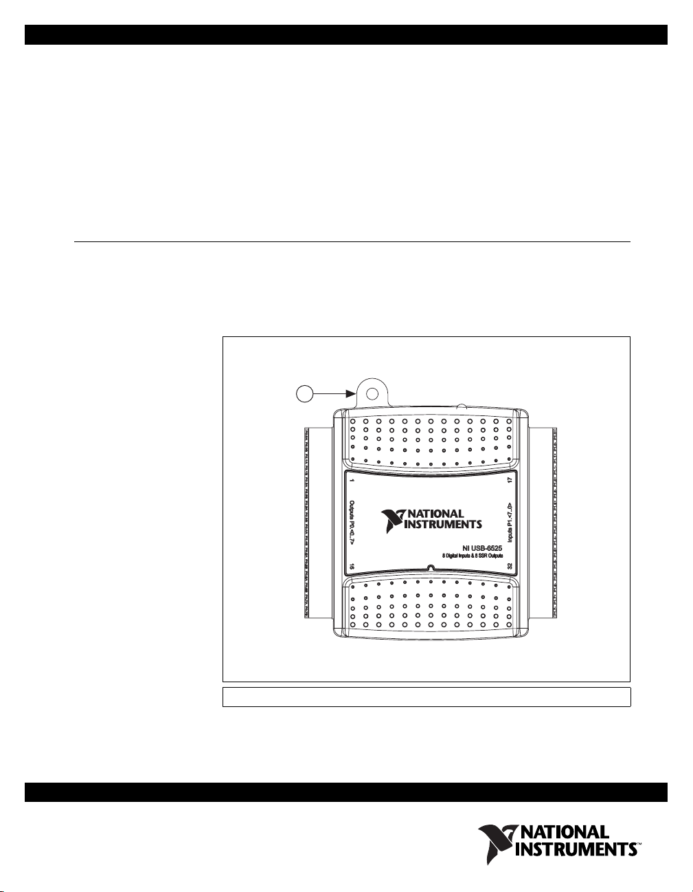
1
1 USB Cable Strain Relief
Figure 1. USB-6525 Top View
Page 2
Installing Software
Software support for the USB-6525 for Windows 2000/XP is provided by
NI-DAQmx.
The NI-DAQmx CD contains example programs that you can use to get
started programming with the USB-6525. Refer to the NI-DAQmx for USB
Devices Getting Started Guide, that shipped with your device and is also
accessible from Start»All Programs»National Instruments»NI-DAQ
for more information.
Note For information about non-Windows operating system support, refer to ni.com/
info
and enter rddqld.
Hardware
The block diagram in Figure 3 shows key functional components of the
USB-6525.
Figure 2. USB-6525 Back View
Vbus
USB Microcontroller
USB
Full-Speed USB Interface
USB-6525 User Guide and Specifications 2 ni.com
P0
P1
Figure 3. USB-6525 Block Diagram
SSRs
Current-
Limiting
Isolated
Inputs
P0.<0..7>A/B
P1.<0..7>+/–
Digital I/O Terminal Block
Page 3
Refer to the Safety Guidelines section of this document for important safety
information.
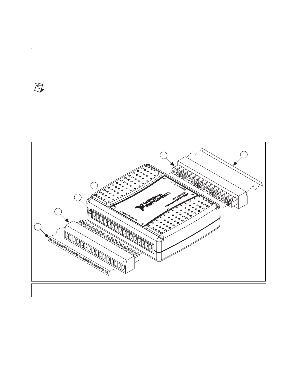
Setting Up Hardware
Complete the following steps to set up the hardware:
1. Install combicon screw terminal blocks by inserting them into the
combicon jacks.
Note The USB-6525 kit ships with signal labels. You can apply the signal labels on the
screw terminal blocks for easy signal identification.
2. Refer to Table 1 and Figure 4 for label orientation and affix provided
signal labels to the screw terminal blocks. Insert the screw terminal
blocks into their respective matching combicon jacks. Refer to
Figure 4 for more information about signal label orientation.
1
2
3
4
1 Overlay Label with Pin Orientation Guides
2 Combicon Jack
3. Connect the wiring to the appropriate screw terminals.
3
3 Screw Terminal Blocks
4 Signal Labels
Figure 4. Signal Label Application Diagram
4
© National Instruments Corporation 3 USB-6525 User Guide and Specifications
Page 4
I/O Connector
The USB-6525 device ships with two detachable terminal blocks for digital
signals. Each individual terminal accepts a wire gauge between
16 AWG–28 AWG.
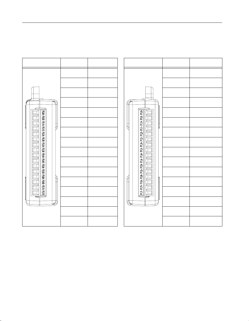
Table 1. Digital Terminal Assignments
Module Terminal Signal Module Terminal Signal
1 P0.0A 17 P1.0+
2 P0.0B 18 P1.0–
3 P0.1A 19 P1.1+
4 P0.1B 20 P1.1–
5 P0.2A 21 P1.2+
6 P0.2B 22 P1.2–
7 P0.3A 23 P1.3+
8 P0.3B 24 P1.3–
9 P0.4A 25 P1.4+
10 P0.4B 26 P1.4–
11 P0.5A 27 P1.5+
12 P0.5B 28 P1.5–
13 P0.6A 29 P1.6+
14 P0.6B 30 P1.6–
15 P0.7A 31 P1.7+/PFI 0+
16 P0.7B 32 P1.7–/PFI 0–
USB-6525 User Guide and Specifications 4 ni.com
Page 5

Signal Descriptions
Table 2 describes the signals available on the I/O connectors.
Table 2. Signal Descriptions
Signal Name Direction Description
P0.<0..7>A/B Output Solid-state relay 60 VDC/30 Vrms (42.4 Vpk) output
P1.<0..6>+/– Input ±60 VDC digital input.
P1.<0..6>+ corresponds to the positive input terminal.
P1.<0..6>– corresponds to the negative input terminal.
P1.7+/– or PFI 0+/– Input This channel is configurable as either a digital input or
an event counter.
Digital Input Signal—±60 VDC digital input.
P1.7+ corresponds to the positive input terminal.
P1.7– corresponds to the negative input terminal.
CTR—As a counter, this signal can be used as an event
counter input source.
PFI 0+ corresponds to the positive counter terminal.
PFI 0– corresponds to the negative counter terminal.
Digital I/O
USB-6525 has eight channel-to-channel optically isolated inputs,
P1.<0..7>, and eight channel-to-channel optically isolated solid-state relay
outputs, P0.<0..7>. P1.7/PFI 0 can also function as a 32-bit counter. Refer
to the Event Counter section for more information about the counter.
Optically Isolated Inputs
The USB-6525 provides eight channels of isolated digital inputs. These
inputs consist of an optocoupler, a depletion-mode MOSFET-based
current-limiting circuit, and Schottky diode.
Each channel has its own positive and negative terminals. The input range
on the channels is –60 VDC to +60 VDC.
Sensing DC Voltages
The USB-6525 detects a wide range of DC signals, from TTL-like logic
levels to DC power supply levels up to 60 V.
© National Instruments Corporation 5 USB-6525 User Guide and Specifications
Page 6

Vcc
Applying a DC voltage of at least 3.2 V across two input terminals registers
logic high. Applying no voltage or a voltage difference of 1 V or less
registers logic low. DC voltages between 1 V and 3.2 V may not register a
consistent or usable value.
Signal Connection Example
Figure 5 shows signal connections for a power supply and load connected
to an isolated input.
Digital
Logic
Computer
Ground
MOSFET-Based
Current-Limiting
Circuitry
Schottky
Isolation
USB-6525
P1.x+
x
P1.
–
Twisted-Pair
Wiring
Load
Figure 5. Connecting a Power Supply and Load to the Isolated Input
Caution
Use twisted-pair field wiring to reduce EMC noise.
In Figure 5, the USB-6525 is sensing a powered load that is connected to
the power supply through a switch.
Note Power supplies must be within the USB-6525 device range. Refer to the
Specifications section for information about these ranges.
When the switch is open, no current flows through the load and no voltage
is applied to the load or to the USB-6525 input. The digital logic of the
USB-6525 then registers a logic low for the channel. When the switch is
closed, current flows through both the load and the USB-6525 optocoupler,
and the USB-6525 registers a logic high for the channel.
+
Vsupply
_
USB-6525 User Guide and Specifications 6 ni.com
Page 7

Solid-State Relay (SSR) Outputs
You can connect loads to the USB-6525. Connect the load to one of the
leads of the power source. Connect either the P0.xA or the P0.xB terminal
to the load and the other terminal to the other lead of the AC or DC power
source. Figure 6 shows a possible configuration where the load is
connected to the P0.xB terminal and the DC or AC power source.
USB-6525
Figure 6. Connecting a Load to the USB-6525
P0.
P0.
x
A
x
B
Twisted-Pair
Wiring
Load
+
or
_
AC
Caution
Use twisted-pair field wiring to reduce EMC noise.
Power-On and Power-Off Conditions
The default power-on state of the solid-state relays is open. By default, the
solid-state relays remain open when the chassis and the USB-6525 device
are powered off.
Protecting Inductive Loads
When inductive loads are connected to the USB-6525 SSR outputs, a large
counter-electromotive force may occur at switching time because of the
energy stored in the inductive load. These flyback voltages can damage the
SSR outputs and/or the external power supply.
Limit flyback voltages at your inductive load by installing one of the
following:
• For DC loads—Install a flyback diode within 18 in. of the load.
• For AC loads—Install a metal oxide varistor (MOV) rated for 30 Vrms
or slightly higher.
© National Instruments Corporation 7 USB-6525 User Guide and Specifications
Page 8

Figures 7 and 8 show examples of using an external flyback diode to
protect DC inductive loads and an MOV to protect AC inductive loads,
respectively.
Flyback Diode for
DC Inductive Loads
P0.x A
P0.
USB-6525
Inductive
Load
x
B
+
V
–
Figure 7. Contact Protection for DC Inductive Loads
MOV for AC
Inductive Loads
P0.x A
USB-6525
P0.
Inductive
Load
x
B
V
DC
AC
Figure 8. Contact Protection for AC Inductive Loads
USB-6525 User Guide and Specifications 8 ni.com
Page 9

Using the USB-6525 as a TTL Output Device
Figure 9 shows a signal connection example for a TTL-level application
with an external supply voltage of +5 V.
To External
+5 V Supply
Event Counter
P0.x A
P0.
x
B
USB-6525
Figure 9. TTL Device Signal Connection Example
Isolated
Ground
V
OUT
When the SSR is open, a small amount of current flows through RL and the
output voltage is close to 5 V, a logic high. When the SSR is closed, current
flows through R
Choose an R
and the output voltage is close to 0 V, a logic low.
L
value small enough to provide the necessary source current
L
but large enough to reduce sink current and to avoid consuming
unnecessary power. Many TTL-level applications use an R
value of 5 kΩ.
L
You can configure PFI 0 (an alias to P1.7) as the source for a 32-bit counter.
In this mode, the device counts low to high transitions on P1.7. The counter
can be armed and disarmed and the count can be read or reset through
software. For more information about event timing requirements, refer to
the Specifications section. Refer to your software documentation for more
information about counter programming techniques.
Specifications
The following specifications are typical at 25 °C, unless otherwise noted.
Isolated Inputs
Number of input channels ...................... 8, ch-ch isolated
Input voltage range................................. –60 VDC to 60 VDC
© National Instruments Corporation 9 USB-6525 User Guide and Specifications
Page 10

Input low voltage –60 VDC 1 VDC
Input high voltage 3.2 VDC 60 VDC
Input current ...........................................3.0 mA/channel max
Solid-State Relay Outputs
Number of output channels.....................8, ch-ch isolated
Relay type ...............................................Normally open solid-state
Switching voltage ...................................60 VDC/30 Vrms max
Switching current (per channel)..............500 mA max, full operation
Switching rate (90% duty cycle) ............5 operations per second
Relay open time ......................................60 μs typ
Relay close time......................................1.2 ms typ
On resistance...........................................550 mΩ max
Level Min Max
relay (SSR)
temperature range
Off state leakage .....................................0.6 μA typ
Counter
Number of counters ................................1 (P1.7 can be configured
as a counter)
Resolution...............................................32 bits
Counter measurements ...........................Rising edge counting
Maximum input frequency .....................5 KHz
Minimum high pulse width.....................20 μs
Minimum low pulse width......................180 μs
Bus Interface
USB specification ...................................USB 2.0 full-speed (12 Mb/s)
USB-6525 User Guide and Specifications 10 ni.com
Page 11

Power Requirements
USB
Input voltage ................................... 4.5 to 5.25 VDC in
Active current ................................. 150 mA max
Suspend current............................... 350 μA typ
Physical Characteristics
Dimensions
Without connectors ......................... 6.35 cm × 8.51 cm × 2.31 cm
With connectors .............................. 8.18 cm × 8.51 cm × 2.31 cm
I/O connectors ........................................ USB series B receptacle,
Screw-terminal wiring............................ 16 to 28 AWG copper conductor
Torque for screw terminals .................... 0.22 – 0.25 N · m
configured state
(2.50 in. × 3.35 in. × 0.91 in.)
(3.22 in. × 3.35 in. × 0.91 in.)
(2) 16 position (screw terminal)
plug headers
wire with 10 mm (0.39 in.) of
insulation stripped from the end
(2.0 – 2.2 lb · in.)
Weight
With connectors .............................. Approx. 87 g (3.1 oz)
Without connectors ......................... Approx. 64 g (2.3 oz)
Safety
Standards
The USB-6525 is designed to meet the requirements of the following
standards of safety for electrical equipment for measurement, control,
and laboratory use:
• IEC 61010-1, EN 61010-1
• UL 61010-1, CSA 61010-1
Note For UL and other safety certifications, refer to the product label, or visit
ni.com/certification, search by model number or product line, and click the
appropriate link in the Certification column.
© National Instruments Corporation 11 USB-6525 User Guide and Specifications
Page 12

Caution Do not use this module for connection to signals or for measurements within
Measurement Categories II, III, or IV.
Environmental
Isolation
Channel-to-channel.................................60 VDC continuous
Channel-to-earth ground.........................60 VDC continuous
Withstand................................................60 VDC continuous
Hazardous Locations
The USB-6525 is not certified for use in hazardous locations.
The USB-6525 device is intended for indoor use only.
Operating temperature
(IEC 60068-2-1 and IEC 60068-2-2)......0 to 55 °C
Operating humidity
(IEC 60068-2-56) ...................................10 to 90% RH, noncondensing
Maximum altitude...................................2,000 m (at 25 °C ambient
temperature)
Storage temperature
(IEC 60068-2-1 and IEC 60068-2-2)......– 40 to 85 °C
Storage humidity
(IEC 60068-2-56) ...................................5 to 90% RH, noncondensing
Pollution Degree (IEC 60664) ................2
Electromagnetic Compatibility
This product is designed to meet the requirements of the following
standards of EMC for electrical equipment for measurement, control,
and laboratory use:
• EN 61326 EMC requirements; Minimum Immunity
• EN 55011 Emissions; Group 1, Class A
• CE, C-Tick, ICES, and FCC Part 15 Emissions; Class A
Note For EMC compliance, operate this device according to product documentation.
USB-6525 User Guide and Specifications 12 ni.com
Page 13

CE Compliance
This product meets the essential requirements of applicable European
Directives, as amended for CE marking, as follows:
• 73/23/EEC; Low-Voltage Directive (safety)
• 89/336/EEC; Electromagnetic Compatibility Directive (EMC)
Note Refer to the Declaration of Conformity (DoC) for this product for any additional
regulatory compliance information. To obtain the DoC for this product, visit
ni.com/certification, search by model number or product line, and click the
appropriate link in the Certification column.
Waste Electrical and Electronic Equipment (WEEE)
EU Customers At the end of their life cycle, all products must be sent to a WEEE recycling
center. For more information about WEEE recycling centers and National Instruments
WEEE initiatives, visit
ni.com/environment/weee.htm.
Safety Guidelines
Caution Operate the hardware only as described in these operating instructions.
The following section contains important safety information that you must
follow when installing and using the USB-6525.
Do not operate the USB-6525 in a manner not specified in this document.
Misuse of the device can result in a hazard. You can compromise the safety
protection built into the device if the device is damaged in any way. If the
device is damaged, contact National Instruments for repair.
Do not substitute parts or modify the device except as described in this
document. Use the device only with the chassis, modules, accessories, and
cables specified in the installation instructions. You must have all covers
and filler panels installed during operation of the device.
Do not operate the device in an explosive atmosphere or where there may
be flammable gases or fumes. If you must operate the device in such an
environment, it must be in a suitably rated enclosure.
If you need to clean the device, use a dry cloth. Make sure that the device
is completely dry and free from contaminants before returning it to service.
© National Instruments Corporation 13 USB-6525 User Guide and Specifications
Page 14

Operate the device only at or below Pollution Degree 2. Pollution is foreign
matter in a solid, liquid, or gaseous state that can reduce dielectric strength
or surface resistivity. The following is a description of pollution degrees:
• Pollution Degree 1 means no pollution or only dry, nonconductive
pollution occurs. The pollution has no influence.
• Pollution Degree 2 means that only nonconductive pollution occurs in
most cases. Occasionally, however, a temporary conductivity caused
by condensation must be expected.
• Pollution Degree 3 means that conductive pollution occurs, or dry,
nonconductive pollution occurs that becomes conductive due to
condensation.
You must insulate signal connections for the maximum voltage for which
the device is rated. Do not exceed the maximum ratings for the device. Do
not install wiring while the device is live with electrical signals. Do not
remove or add connector blocks when power is connected to the system.
Avoid contact between your body and the connector block signal when hot
swapping modules. Remove power from signal lines before connecting
them to or disconnecting them from the device.
Operate the device at or below the Measurement Category I
circuits are subjected to working voltages
2
and transient stresses
1
. Measurement
(overvoltage) from the circuit to which they are connected during
measurement or test. Measurement categories establish standard impulse
withstand voltage levels that commonly occur in electrical distribution
systems. The following is a description of measurement categories:
• Measurement Category I is for measurements performed on circuits
not directly connected to the electrical distribution system referred to
as MAINS
3
voltage. This category is for measurements of voltages
from specially protected secondary circuits. Such voltage
measurements include signal levels, special equipment, limited-energy
parts of equipment, circuits powered by regulated low-voltage sources,
and electronics.
• Measurement Category II is for measurements performed on circuits
directly connected to the electrical distribution system. This category
refers to local-level electrical distribution, such as that provided by a
standard wall outlet (for example, 115 V for U.S. or 230 V for Europe).
Examples of Measurement Category II are measurements performed
on household appliances, portable tools, and similar USB devices.
1
Measurement Category as defined in electrical safety standard IEC 61010-1. Measurement Category is also referred to as
Installation Category.
2
Working Voltage is the highest rms value of an AC or DC voltage that can occur across any particular insulation.
3
MAINS is defined as a hazardous live electrical supply system that powers equipment. Suitably rated measuring circuits may
be connected to the MAINS for measuring purposes.
USB-6525 User Guide and Specifications 14 ni.com
Page 15

• Measurement Category III is for measurements performed in the
building installation at the distribution level. This category refers to
measurements on hard-wired equipment such as equipment in fixed
installations, distribution boards, and circuit breakers. Other examples
are wiring, including cables, bus-bars, junction boxes, switches,
socket-outlets in the fixed installation, and stationary motors with
permanent connections to fixed installations.
Measurement Category IV is for measurements performed at the primary
electrical supply installation (<1,000 V). Examples include electricity
meters and measurements on primary overcurrent protection devices and
on ripple control units.
Where to Go for Support
The National Instruments Web site is your complete resource for technical
support. At
troubleshooting and application development self-help resources to email
and phone assistance from NI Application Engineers.
A Declaration of Conformity (DoC) is our claim of compliance with the
Council of the European Communities using the manufacturer’s
declaration of conformity. This system affords the user protection for
electronic compatibility (EMC) and product safety. You can obtain the DoC
for your product by visiting
supports calibration, you can obtain the calibration certificate for your
product at
ni.com/support you have access to everything from
ni.com/calibration.
ni.com/certification. If your product
National Instruments corporate headquarters is located at
11500 North Mopac Expressway, Austin, Texas, 78759-3504.
National Instruments also has offices located around the world to help
address your support needs. For telephone support in the United States,
create your service request at
instructions or dial 512 795 8248. For telephone support outside the United
States, contact your local branch office:
Australia 1800 300 800, Austria 43 0 662 45 79 90 0,
Belgium32027570020, Brazil551132623599,
Canada 800 433 3488, China 86 21 6555 7838,
Czech Republic 420 224 235 774, Denmark 45 45 76 26 00,
Finland3850972572511, France330148142424,
Germany 49 0 89 741 31 30, India 91 80 51190000,
Israel 972 0 3 6393737, Italy 39 02 413091, Japan 81 3 5472 2970,
Korea820234513400, Lebanon96101332828,
Malaysia 1800 887710, Mexico 01 800 010 0793,
Netherlands 31 0 348 433 466, New Zealand 0800 553 322,
© National Instruments Corporation 15 USB-6525 User Guide and Specifications
ni.com/support and follow the calling
Page 16

Norway 47 0 66 90 76 60, Poland 48 22 3390150,
Portugal 351 210 311 210, Russia 7 495 783 68 51,
Singapore 1800 226 5886, Slovenia 386 3 425 42 00,
South Africa 27 0 11 805 8197, Spain 34 91 640 0085,
Sweden460858789500, Switzerland41562005151,
Taiwan 886 02 2377 2222, Thailand 662 278 6777,
United Kingdom 44 0 1635 523545
National Instruments, NI, ni.com, and LabVIEW are trademarks of National Instruments Corporation.
Refer to the Terms of Use section on ni.com/legal for more information about National
Instruments trademarks. Other product and company names mentioned herein are trademarks or trad e
names of their respective companies. For patents covering National Instruments products, refer to the
appropriate location: Help»Patents in your software, the patents.txt file on your CD, or
ni.com/patents.
© 2006 National Instruments Corporation. All rights reserved.
371818A-01 Oct06
 Loading...