

Page 1

DAQ M Series
NI USB-621x User Manual
Bus-Powered M Series USB Devices
NI USB-621x User Manual
August 2006
371931A-01
Page 2

Support
Worldwide Technical Support and Product Information
ni.com
National Instruments Corporate Headquarters
11500 North Mopac Expressway Austin, Texas 78759-3504 USA Tel: 512 683 0100
Worldwide Offices
Australia 1800 300 800, Austria 43 0 662 45 79 90 0, Belgium 32 0 2 757 00 20, Brazil 55 11 3262 3599,
Canada 800 433 3488, China 86 21 6555 7838, Czech Republic 420 224 235 774, Denmark 45 45 76 26 00,
Finland 385 0 9 725 725 11, France 33 0 1 48 14 24 24, Germany 49 0 89 741 31 30, India 91 80 41190000,
Israel 972 0 3 6393737, Italy 39 02 413091, Japan 81 3 5472 2970, Korea 82 02 3451 3400,
Lebanon 961 0 1 33 28 28, Malaysia 1800 887710, Mexico 01 800 010 0793, Netherlands 31 0 348 433 466,
New Zealand 0800 553 322, Norway 47 0 66 90 76 60, Poland 48 22 3390150, Portugal 351 210 311 210,
Russia 7 095 783 68 51, Singapore 1800 226 5886, Slovenia 386 3 425 4200, South Africa 27 0 11 805 8197,
Spain 34 91 640 0085, Sweden 46 0 8 587 895 00, Switzerland 41 56 200 51 51, Taiwan 886 02 2377 2222,
Thailand 662 278 6777, United Kingdom 44 0 1635 523545
For further support information, refer to the Technical Support and Professional Services appendix. To comment
on National Instruments documentation, refer to the National Instruments Web site at
the info code
feedback.
ni.com/info and enter
© 2006 National Instruments Corporation. All rights reserved.
Page 3

Important Information
Warranty
The USB-6210, USB-6211, USB-6215, and USB-6218 devices are warranted against defects in materials and workmanship for a period of
three years from the date of shipment, as evidenced by receipts or other documentation. National Instruments will, at its option, repair or replace
equipment that proves to be defective during the warranty period. This warranty includes parts and labor.
The media on which you receive National Instruments software are warranted not to fail to execute programming instructions, due to defects in
materials and workmanship, for a period of 90 days from date of shipment, as evidenced by receipts or other documentation. National Instruments
will, at its option, repair or replace software media that do not execute programming instruc tions if National Instruments receives notice of such defects
during the warranty period. National Instruments does not warrant that the operation of the software shall be uninterrupted or error free.
A Return Material Authorization (RMA) number must be obtained from the factory and clearly marked on the outside of the package before any
equipment will be accepted for warranty work. National Instruments will pay the shipping costs of returning to the owner parts which are covered by
warranty.
National Instruments believes that the information in this document is accurate. The document has been carefully reviewed for technical accuracy. In
the event that technical or typographical errors exist, National Instruments reserves the right to make changes to subsequent editions of this document
without prior notice to holders of this edition. The reader should consult National Instruments if errors are suspected. In no event shall National
Instruments be liable for any damages arising out of or related to this document or the information contained in it.
E
XCEPT AS SPECIFIED HEREIN, NATIONAL INSTRUMENTS MAKES NO WARRANTIES, EXPRESS OR IMPLIED, AND SPECIFICALLY DISCLAIMS ANY WARRANTY OF
MERCHANTABILITY OR FITNESS FOR A PARTICULAR PURPOSE. CUSTOMER’S RIGHT TO RECOVER DAMAGES CAUSED BY FAULT OR NEGLIGENCE ON THE PART OF NATIONAL
I
NSTRUMENTS SHALL BE LIMITED TO THE AMOUNT THERETOFORE PAID BY THE CUSTOMER. NATIONAL INSTRUMENTS WILL NOT BE LIABLE FOR DAMAGES RESULTING
FROM LOSS OF DATA, PROFITS, USE OF PRODUCTS, OR INCIDENTAL OR CONSEQUENTIAL DAMAGES, EVEN IF ADVISED OF THE POSSIBILITY THEREOF. This limitation of
the liability of National Instruments will apply regardless of the form of action, whether in contract or tort, including negligence. Any action against
National Instruments must be brought within one year after the cause of action accrues. National Instruments shall not be liable for any delay in
performance due to causes beyond its reasonable control. The warranty provided herein does not cover damages, defects, malfunctions, or service
failures caused by owner’s failure to follow the National Instruments installation, operation, or maintenance instructions; owner’s modification of the
product; owner’s abuse, misuse, or negligent acts; and power failure or surges, fire, flood, accident, actions of third parties, or other events outside
reasonable control.
Copyright
Under the copyright laws, this publication may not be reproduced or transmitted in any form, electronic or mechanical, including photocopying,
recording, storing in an information retrieval system, or translating, in whole or in part, without the prior written consent of National
Instruments Corporation.
National Instruments respects the intellectual property of others, and we ask our users to do the same. NI software is protected by copyright and other
intellectual property laws. Where NI software may be used to reproduce software or other materials belonging to others, you may use NI software only
to reproduce materials that you may reproduce in accordance with the terms of any applicable license or other legal restriction.
Trademarks
National Instruments, NI, ni.com, and LabVIEW are trademarks of National Instruments Corporation. Refer to the Terms of Use section
on
ni.com/legal for more information about National Instruments trademarks.
®
is the registered trademark of Apple Computer, Inc. Other product and company names mentioned herein are trademarks or trade names
FireWire
of their respective companies.
Members of the National Instruments Alliance Partner Program are business entities independent from National Instruments and have no agency,
partnership, or joint-venture relationship with National Instruments.
Patents
For patents covering National Instruments products, refer to the appropriate location: Help»Patents in your software, the patents.txt file
on your CD, or
ni.com/patents.
WARNING REGARDING USE OF NATIONAL INSTRUMENTS PRODUCTS
(1) NATIONAL INSTRUMENTS PRODUCTS ARE NOT DESIGNED WITH COMPONENTS AND TESTING FOR A LEVEL OF
RELIABILITY SUITABLE FOR USE IN OR IN CONNECTION WITH SURGICAL IMPLANTS OR AS CRITICAL COMPONENTS IN
ANY LIFE SUPPORT SYSTEMS WHOSE FAILURE TO PERFORM CAN REASONABLY BE EXPECTED TO CAUSE SIGNIFICANT
INJURY TO A HUMAN.
(2) IN ANY APPLICATION, INCLUDING THE ABOVE, RELIABILITY OF OPERATION OF THE SOFTWARE PRODUCTS CAN BE
IMPAIRED BY ADVERSE FACTORS, INCLUDING BUT NOT LIMITED TO FLUCTUATIONS IN ELECTRICAL POWER SUPPLY,
COMPUTER HARDWARE MALFUNCTIONS, COMPUTER OPERATING SYSTEM SOFTWARE FITNESS, FITNESS OF COMPILERS
AND DEVELOPMENT SOFTWARE USED TO DEVELOP AN APPLICATION, INSTALLATION ERRORS, SOFTWARE AND HARDWARE
COMPATIBILITY PROBLEMS, MALFUNCTIONS OR FAILURES OF ELECTRONIC MONITORING OR CONTROL DEVICES,
TRANSIENT FAILURES OF ELECTRONIC SYSTEMS (HARDWARE AND/OR SOFTWARE), UNANTICIPATED USES OR MISUSES, OR
ERRORS ON THE PART OF THE USER OR APPLICATIONS DESIGNER (ADVERSE FACTORS SUCH AS THESE ARE HEREAFTER
COLLECTIVELY TERMED “SYSTEM FAILURES”). ANY APPLICATION WHERE A SYSTEM FAILURE WOULD CREATE A RISK OF
HARM TO PROPERTY OR PERSONS (INCLUDING THE RISK OF BODILY INJURY AND DEATH) SHOULD NOT BE RELIANT SOLELY
UPON ONE FORM OF ELECTRONIC SYSTEM DUE TO THE RISK OF SYSTEM FAILURE. TO AVOID DAMAGE, INJURY, OR DEATH,
THE USER OR APPLICATION DESIGNER MUST TAKE REASONABLY PRUDENT STEPS TO PROTECT AGAINST SYSTEM FAILURES,
INCLUDING BUT NOT LIMITED TO BACK-UP OR SHUT DOWN MECHANISMS. BECAUSE EACH END-USER SYSTEM IS
CUSTOMIZED AND DIFFERS FROM NATIONAL INSTRUMENTS' TESTING PLATFORMS AND BECAUSE A USER OR APPLICATION
DESIGNER MAY USE NATIONAL INSTRUMENTS PRODUCTS IN COMBINATION WITH OTHER PRODUCTS IN A MANNER NOT
EVALUATED OR CONTEMPLATED BY NATIONAL INSTRUMENTS, THE USER OR APPLICATION DESIGNER IS ULTIMATELY
RESPONSIBLE FOR VERIFYING AND VALIDATING THE SUITABILITY OF NATIONAL INSTRUMENTS PRODUCTS WHENEVER
Page 4

NATIONAL INSTRUMENTS PRODUCTS ARE INCORPORATED IN A SYSTEM OR APPLICATION, INCLUDING, WITHOUT
LIMITATION, THE APPROPRIATE DESIGN, PROCESS AND SAFETY LEVEL OF SUCH SYSTEM OR APPLICATION.
Page 5

Contents
About This Manual
Conventions ...................................................................................................................xiii
Related Documentation..................................................................................................xiv
NI-DAQmx for Windows................................................................................xiv
LabVIEW ........................................................................................................xiv
LabWindows™/CVI™....................................................................................xv
Measurement Studio........................................................................................xv
ANSI C without NI Application Software ......................................................xv
.NET Languages without NI Application Software ........................................xvi
Device Documentation and Specifications......................................................xvi
Training Courses .............................................................................................xvi
Technical Support on the Web ........................................................................xvi
Chapter 1
Getting Started
Installing NI-DAQmx ....................................................................................................1-2
Installing Other Software...............................................................................................1-2
Installing the Hardware..................................................................................................1-3
Device Pinouts ...............................................................................................................1-3
Device Specifications ....................................................................................................1-3
Device Accessories ........................................................................................................1-3
Chapter 2
DAQ System Overview
DAQ Hardware ..............................................................................................................2-1
DAQ-STC2......................................................................................................2-2
Calibration Circuitry........................................................................................2-2
Signal Conditioning .......................................................................................................2-3
Sensors and Transducers .................................................................................2-3
Programming Devices in Software ................................................................................2-4
Chapter 3
Connector Information
I/O Connector Signal Descriptions ................................................................................3-1
+5 V Power ....................................................................................................................3-2
+5 V Power as an Output ................................................................................3-2
+5 V Power as an Input ...................................................................................3-3
© National Instruments Corporation v NI USB-621x User Manual
Page 6

Contents
Chapter 4
Analog Input
Analog Input Circuitry .................................................................................................. 4-1
Analog Input Range....................................................................................................... 4-2
Analog Input Ground-Reference Settings ..................................................................... 4-3
Multichannel Scanning Considerations ......................................................................... 4-6
Analog Input Data Acquisition Methods....................................................................... 4-9
Analog Input Digital Triggering.................................................................................... 4-10
Field Wiring Considerations..........................................................................................4-11
Analog Input Timing Signals ........................................................................................ 4-11
Configuring AI Ground-Reference Settings in Software................................ 4-5
Use Low Impedance Sources.......................................................................... 4-6
Carefully Choose the Channel Scanning Order ..............................................4-7
Avoid Switching from a Large to a Small Input Range ................... 4-7
Insert Grounded Channel between Signal Channels ........................ 4-7
Minimize Voltage Step between Adjacent Channels ....................... 4-8
Avoid Scanning Faster Than Necessary ......................................................... 4-8
Example 1 ......................................................................................... 4-8
Example 2 ......................................................................................... 4-9
Software-Timed Acquisitions ......................................................................... 4-9
Hardware-Timed Acquisitions........................................................................ 4-9
Buffered ............................................................................................ 4-10
Non-Buffered.................................................................................... 4-10
AI Sample Clock Signal.................................................................................. 4-14
Using an Internal Source .................................................................. 4-15
Using an External Source ................................................................. 4-15
Routing AI Sample Clock Signal to an Output Terminal................. 4-15
Other Timing Requirements ............................................................. 4-15
AI Sample Clock Timebase Signal ................................................................. 4-16
AI Convert Clock Signal................................................................................. 4-16
Using an Internal Source .................................................................. 4-17
Using an External Source ................................................................. 4-17
Routing AI Convert Clock Signal to an Output Terminal ................ 4-17
Using a Delay from Sample Clock to Convert Clock ...................... 4-17
Other Timing Requirements ............................................................. 4-18
AI Convert Clock Timebase Signal ................................................................ 4-20
AI Hold Complete Event Signal ..................................................................... 4-21
AI Start Trigger Signal.................................................................................... 4-21
Using a Digital Source...................................................................... 4-21
Routing AI Start Trigger to an Output Terminal .............................. 4-21
AI Reference Trigger Signal ........................................................................... 4-22
Using a Digital Source...................................................................... 4-23
Routing AI Reference Trigger Signal to an Output Terminal .......... 4-23
NI USB-621x User Manual vi ni.com
Page 7

AI Pause Trigger Signal ..................................................................................4-23
Using a Digital Source ......................................................................4-23
Getting Started with AI Applications in Software.........................................................4-24
Chapter 5
Connecting AI Signals on the USB-6210/6211 Devices
Connecting Floating Signal Sources..............................................................................5-3
What Are Floating Signal Sources? ................................................................5-3
When to Use Differential Connections with Floating Signal Sources ............5-3
When to Use Referenced Single-Ended (RSE) Connections with
Floating Signal Sources................................................................................5-3
When to Use Non-Referenced Single-Ended (NRSE) Connections
with Floating Signal Sources........................................................................5-4
Using Differential Connections for Floating Signal Sources ..........................5-5
Using Non-Referenced Single-Ended (NRSE) Connections for
Floating Signal Sources................................................................................5-8
Using Referenced Single-Ended (RSE) Connections for Floating
Signal Sources ..............................................................................................5-9
Connecting Ground-Referenced Signal Sources ...........................................................5-9
What Are Ground-Referenced Signal Sources? ..............................................5-9
When to Use Differential Connections with Ground-Referenced
Signal Sources ..............................................................................................5-10
When to Use Non-Referenced Single-Ended (NRSE) Connections with
Ground-Referenced Signal Sources..............................................................5-10
When to Use Referenced Single-Ended (RSE) Connections with
Ground-Referenced Signal Sources..............................................................5-11
Using Differential Connections for Ground-Referenced Signal Sources........5-12
Using Non-Referenced Single-Ended (NRSE) Connections for
Ground-Referenced Signal Sources..............................................................5-13
Contents
Chapter 6
Connecting AI Signals on the USB-6215/6218 Devices
Differential Measurements ............................................................................................6-1
Differential Pairs............................................................................................................6-1
Referenced Single-Ended (RSE) Measurements ...........................................................6-3
Non-Referenced Single-Ended (NRSE) Measurements ................................................6-4
© National Instruments Corporation vii NI USB-621x User Manual
Page 8

Contents
Chapter 7
Analog Output
Analog Output Circuitry................................................................................................ 7-1
AO Range ...................................................................................................................... 7-2
Minimizing Glitches on the Output Signal.................................................................... 7-2
Analog Output Data Generation Methods ..................................................................... 7-2
Software-Timed Generations .......................................................................... 7-2
Hardware-Timed Generations......................................................................... 7-2
Analog Output Digital Triggering................................................................................. 7-4
Connecting Analog Output Signals ............................................................................... 7-4
Analog Output Timing Signals...................................................................................... 7-5
AO Start Trigger Signal .................................................................................. 7-5
AO Pause Trigger Signal ................................................................................ 7-6
AO Sample Clock Signal ................................................................................ 7-7
AO Sample Clock Timebase Signal................................................................ 7-8
Getting Started with AO Applications in Software....................................................... 7-9
Using a Digital Source...................................................................... 7-5
Routing AO Start Trigger Signal to an Output Terminal ................. 7-6
Using a Digital Source...................................................................... 7-6
Using an Internal Source .................................................................. 7-7
Using an External Source ................................................................. 7-7
Routing AO Sample Clock Signal to an Output Terminal ............... 7-7
Other Timing Requirements ............................................................. 7-7
Chapter 8
Digital I/O
Static DIO......................................................................................................................8-2
I/O Protection ................................................................................................................ 8-2
Increasing Current Drive ............................................................................................... 8-2
Connecting Digital I/O Signals ..................................................................................... 8-3
Getting Started with DIO Applications in Software...................................................... 8-4
Chapter 9
Counters
Counter Input Applications ........................................................................................... 9-2
Counting Edges ............................................................................................... 9-2
Single Point (On-Demand) Edge Counting ...................................... 9-2
Buffered (Sample Clock) Edge Counting......................................... 9-3
Non-Cumulative Buffered Edge Counting ....................................... 9-4
Controlling the Direction of Counting.............................................. 9-4
NI USB-621x User Manual viii ni.com
Page 9

Contents
Pulse-Width Measurement ..............................................................................9-5
Single Pulse-Width Measurement.....................................................9-5
Buffered Pulse-Width Measurement.................................................9-5
Period Measurement........................................................................................9-6
Single Period Measurement ..............................................................9-7
Buffered Period Measurement ..........................................................9-7
Semi-Period Measurement ..............................................................................9-9
Single Semi-Period Measurement.....................................................9-9
Buffered Semi-Period Measurement.................................................9-9
Frequency Measurement .................................................................................9-10
Method 1—Measure Low Frequency with One Counter..................9-10
Method 1b—Measure Low Frequency with One Counter
(Averaged)......................................................................................9-11
Method 2—Measure High Frequency with Two Counters...............9-11
Method 3—Measure Large Range of Frequencies Using
Two Counters .................................................................................9-12
Choosing a Method for Measuring Frequency .................................9-13
Position Measurement .....................................................................................9-15
Measurements Using Quadrature Encoders......................................9-15
Measurements Using Two Pulse Encoders.......................................9-17
Two-Signal Edge-Separation Measurement....................................................9-18
Single Two-Signal Edge-Separation Measurement ..........................9-18
Buffered Two-Signal Edge-Separation Measurement ......................9-19
Counter Output Applications .........................................................................................9-20
Simple Pulse Generation .................................................................................9-20
Single Pulse Generation ....................................................................9-20
Single Pulse Generation with Start Trigger ......................................9-20
Retriggerable Single Pulse Generation .............................................9-21
Pulse Train Generation ....................................................................................9-22
Continuous Pulse Train Generation ..................................................9-22
Frequency Generation .....................................................................................9-23
Using the Frequency Generator ........................................................9-23
Frequency Division .........................................................................................9-24
Pulse Generation for ETS................................................................................9-24
Counter Timing Signals.................................................................................................9-25
Counter n Source Signal..................................................................................9-26
Routing a Signal to Counter n Source...............................................9-26
Routing Counter n Source to an Output Terminal ............................9-26
Counter n Gate Signal .....................................................................................9-27
Routing a Signal to Counter n Gate ..................................................9-27
Routing Counter n Gate to an Output Terminal................................9-27
Counter n Aux Signal ......................................................................................9-27
Routing a Signal to Counter n Aux ...................................................9-27
© National Instruments Corporation ix NI USB-621x User Manual
Page 10

Contents
Counter n A, Counter n B, and Counter n Z Signals ...................................... 9-28
Routing Signals to A, B, and Z Counter Inputs................................ 9-28
Counter n Up_Down Signal............................................................................ 9-28
Counter n HW Arm Signal.............................................................................. 9-28
Routing Signals to Counter n HW Arm Input.................................. 9-28
Counter n Internal Output and Counter n TC Signals..................................... 9-29
Routing Counter n Internal Output to an Output Terminal .............. 9-29
Frequency Output Signal ................................................................................ 9-29
Routing Frequency Output to a Terminal......................................... 9-29
Default Counter/Timer Pinouts ..................................................................................... 9-29
Counter Triggering ........................................................................................................ 9-31
Arm Start Trigger............................................................................................ 9-31
Start Trigger .................................................................................................... 9-31
Pause Trigger .................................................................................................. 9-31
Other Counter Features.................................................................................................. 9-32
Sample Clock .................................................................................................. 9-32
Cascading Counters......................................................................................... 9-33
Counter Filters................................................................................................. 9-33
Prescaling ........................................................................................................ 9-34
Duplicate Count Prevention ............................................................................ 9-35
Example Application That Works Correctly
(No Duplicate Counting) ............................................................... 9-36
Example Application That Works Incorrectly
(Duplicate Counting) ..................................................................... 9-37
Example Application That Prevents Duplicate Count...................... 9-37
Enabling Duplicate Count Prevention in NI-DAQmx...................... 9-38
Chapter 10
PFI
Using PFI Terminals as Timing Input Signals .............................................................. 10-2
Exporting Timing Output Signals Using PFI Terminals............................................... 10-3
Using PFI Terminals as Static Digital I/Os ................................................................... 10-3
Connecting PFI Input Signals........................................................................................ 10-3
PFI Filters ...................................................................................................................... 10-4
I/O Protection ................................................................................................................ 10-6
Programmable Power-Up States.................................................................................... 10-6
NI USB-621x User Manual x ni.com
Page 11

Chapter 11
Isolation and Digital Isolators
Digital Isolation .............................................................................................................11-2
Benefits of an Isolated DAQ Device .............................................................................11-2
Reducing Common-Mode Noise ...................................................................................11-2
Creating an AC Return Path............................................................................11-3
Isolated Systems................................................................................11-3
Non-Isolated Systems .......................................................................11-3
Chapter 12
Digital Routing and Clock Generation
80 MHz Timebase..........................................................................................................12-1
20 MHz Timebase..........................................................................................................12-1
100 kHz Timebase .........................................................................................................12-2
Chapter 13
Bus Interface
USB Signal Streams.......................................................................................................13-1
Data Transfer Methods ..................................................................................................13-1
USB Signal Stream..........................................................................................13-1
Programmed I/O ..............................................................................................13-2
Changing Data Transfer Methods ...................................................................13-2
Contents
Chapter 14
Triggering
Triggering with a Digital Source ...................................................................................14-1
Appendix A
Device-Specific Information
USB-6210 ......................................................................................................................A-1
USB-6211/6215 .............................................................................................................A-4
USB 6218.......................................................................................................................A-7
© National Instruments Corporation xi NI USB-621x User Manual
Page 12

Contents
Appendix B
Troubleshooting
Appendix C
Technical Support and Professional Services
Glossary
Index
Device Pinouts
Figure A-1. USB-6210 Pinout .................................................................................. A-2
Figure A-2. USB-6211/6215 Pinout ......................................................................... A-5
Figure A-3. USB 6218 Pinout .................................................................................. A-8
NI USB-621x User Manual xii ni.com
Page 13

About This Manual
The NI 621x User Manual contains information about using the National
Instruments USB-621x data acquisition (DAQ) devices with
NI-DAQmx 8.3 and later. NI 621x devices feature up to 32 analog input
(AI) channels, up to two analog output (AO) channels, up to eight lines of
digital input (DI), up to eight lines of digital output (DO), and two counters.
Conventions
The following conventions are used in this manual:
<> Angle brackets that contain numbers separated by an ellipsis represent
a range of values associated with a bit or signal name—for example,
AO <3..0>.
» The » symbol leads you through nested menu items and dialog box options
to a final action. The sequence File»Page Setup»Options directs you to
pull down the File menu, select the Page Setup item, and select Options
from the last dialog box.
This icon denotes a note, which alerts you to important information.
This icon denotes a caution, which advises you of precautions to take to
avoid injury, data loss, or a system crash. When this symbol is marked on a
product, refer to the Read Me First: Safety and Radio-Frequency
Interference document which can be found at
information about precautions to take.
bold Bold text denotes items that you must select or click in the software, such
as menu items and dialog box options. Bold text also denotes parameter
names.
italic Italic text denotes variables, emphasis, a cross-reference, or an introduction
to a key concept. Italic text also denotes text that is a placeholder for a word
or value that you must supply.
monospace Text in this font denotes text or characters that you should enter from the
keyboard, sections of code, programming examples, and syntax examples.
This font is also used for the proper names of disk drives, paths, directories,
programs, subprograms, subroutines, device names, functions, operations,
variables, filenames, and extensions.
© National Instruments Corporation xiii NI USB-621x User Manual
ni.com/manuals, for
Page 14

About This Manual
Related Documentation
Each application software package and driver includes information about
writing applications for taking measurements and controlling measurement
devices. The following references to documents assume you have
NI-DAQ 8.3 or later, and where applicable, version 7.0 or later of the NI
application software.
NI-DAQmx for Windows
The NI-DAQmx for USB Devices Getting Started Guide describes
how to install your NI-DAQmx for Windows software, your
NI-DAQmx-supported DAQ device, and how to confirm that your device is
operating properly. Select Start»All Programs»National Instruments»
NI-DAQ»NI-DAQmx for USB Devices Getting Started.
The NI-DAQ Readme lists which devices are supported by this version of
NI-DAQ. Select Start»All Programs»National Instruments»NI-DAQ»
NI-DAQ Readme.
The NI-DAQmx Help contains general information about measurement
concepts, key NI-DAQmx concepts, and common applications that are
applicable to all programming environments. Select Start»All Programs»
National Instruments»NI-DAQ»NI-DAQmx Help.
LabVIEW
If you are a new user, use the Getting Started with LabVIEW manual to
familiarize yourself with the LabVIEW graphical programming
environment and the basic LabVIEW features you use to build data
acquisition and instrument control applications. Open the Getting Started
with LabVIEW manual by selecting Start»All Programs»National
Instruments»LabVIEW»LabVIEW Manuals or by navigating to the
labview\manuals directory and opening
LV_Getting_Started.pdf.
Use the LabVIEW Help, available by selecting Help»Search the
LabVIEW Help in LabVIEW, to access information about LabVIEW
programming concepts, step-by-step instructions for using LabVIEW, and
reference information about LabVIEW VIs, functions, palettes, menus, and
NI USB-621x User Manual xiv ni.com
Page 15

About This Manual
tools. Refer to the following locations on the Contents tab of the LabVIEW
Help for information about NI-DAQmx:
• Getting Started»Getting Started with DAQ—Includes overview
information and a tutorial to learn how to take an NI-DAQmx
measurement in LabVIEW using the DAQ Assistant.
• VI and Function Reference»Measurement I/O VIs and
Functions—Describes the LabVIEW NI-DAQmx VIs and properties.
• Taking Measurements—Contains the conceptual and how-to
information you need to acquire and analyze measurement data in
LabVIEW, including common measurements, measurement
fundamentals, NI-DAQmx key concepts, and device considerations.
LabWindows™/CVI
™
The Data Acquisition book of the LabWindows/CVI Help contains
measurement concepts for NI-DAQmx. This book also contains Taking an
NI-DAQmx Measurement in LabWindows/CVI, which includes
step-by-step instructions about creating a measurement task using the DAQ
Assistant. In LabWindows/CVI, select Help»Contents, then select Using
LabWindows/CVI»Data Acquisition.
The NI-DAQmx Library book of the LabWindows/CVI Help contains API
overviews and function reference for NI-DAQmx. Select Library
Reference»NI-DAQmx Library in the LabWindows/CVI Help.
Measurement Studio
The NI Measurement Studio Help contains function reference,
measurement concepts, and a walkthrough for using the Measurement
Studio NI-DAQmx .NET and Visual C++ class libraries. This help
collection is integrated into the Microsoft Visual Studio .NET
documentation. In Visual Studio .NET, select Help»Contents.
Note You must have Visual Studio .NET installed to view the NI Measurement Studio
Help.
ANSI C without NI Application Software
The NI-DAQmx Help contains API overviews and general information
about measurement concepts. Select Start»All Programs»National
Instruments»NI-DAQmx Help.
© National Instruments Corporation xv NI USB-621x User Manual
Page 16

About This Manual
.NET Languages without NI Application Software
The NI Measurement Studio Help contains function reference and
measurement concepts for using the Measurement Studio NI-DAQmx
.NET and Visual C++ class libraries. This help collection is integrated into
the Visual Studio .NET documentation. In Visual Studio .NET, select
Help»Contents.
Note You must have Visual Studio .NET installed to view the NI Measurement Studio
Help.
Device Documentation and Specifications
The NI 621x Specifications contains all specifications for the USB-6210,
USB-6211, USB-6215, and USB-6218 M Series devices.
NI-DAQ 7.0 and later includes the Device Document Browser, which
contains online documentation for supported DAQ, SCXI, and switch
devices, such as help files describing device pinouts, features, and
operation, and PDF files of the printed device documents. You can find,
view, and/or print the documents for each device using the Device
Document Browser at any time by inserting the CD. After installing the
Device Document Browser, device documents are accessible from Start»
All Programs»National Instruments»NI-DAQ»Browse Device
Documentation.
Training Courses
If you need more help getting started developing an application with NI
products, NI offers training courses. To enroll in a course or obtain a
detailed course outline, refer to
ni.com/training.
Technical Support on the Web
For additional support, refer to ni.com/support or zone.ni.com.
Note You can download these documents at
DAQ specifications and some DAQ manuals are available as PDFs. You
must have Adobe Acrobat Reader with Search and Accessibility 5.0.5 or
later installed to view the PDFs. Refer to the Adobe Systems Incorporated
Web site at
National Instruments Product Manuals Library at
updated documentation resources.
NI USB-621x User Manual xvi ni.com
www.adobe.com to download Acrobat Reader. Refer to the
ni.com/manuals.
ni.com/manuals for
Page 17
Getting Started
1
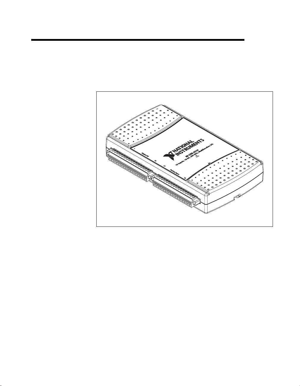
Figure 1-1. USB-6210/6211
© National Instruments Corporation 1-1 NI USB-621x User Manual
Page 18
Chapter 1 Getting Started
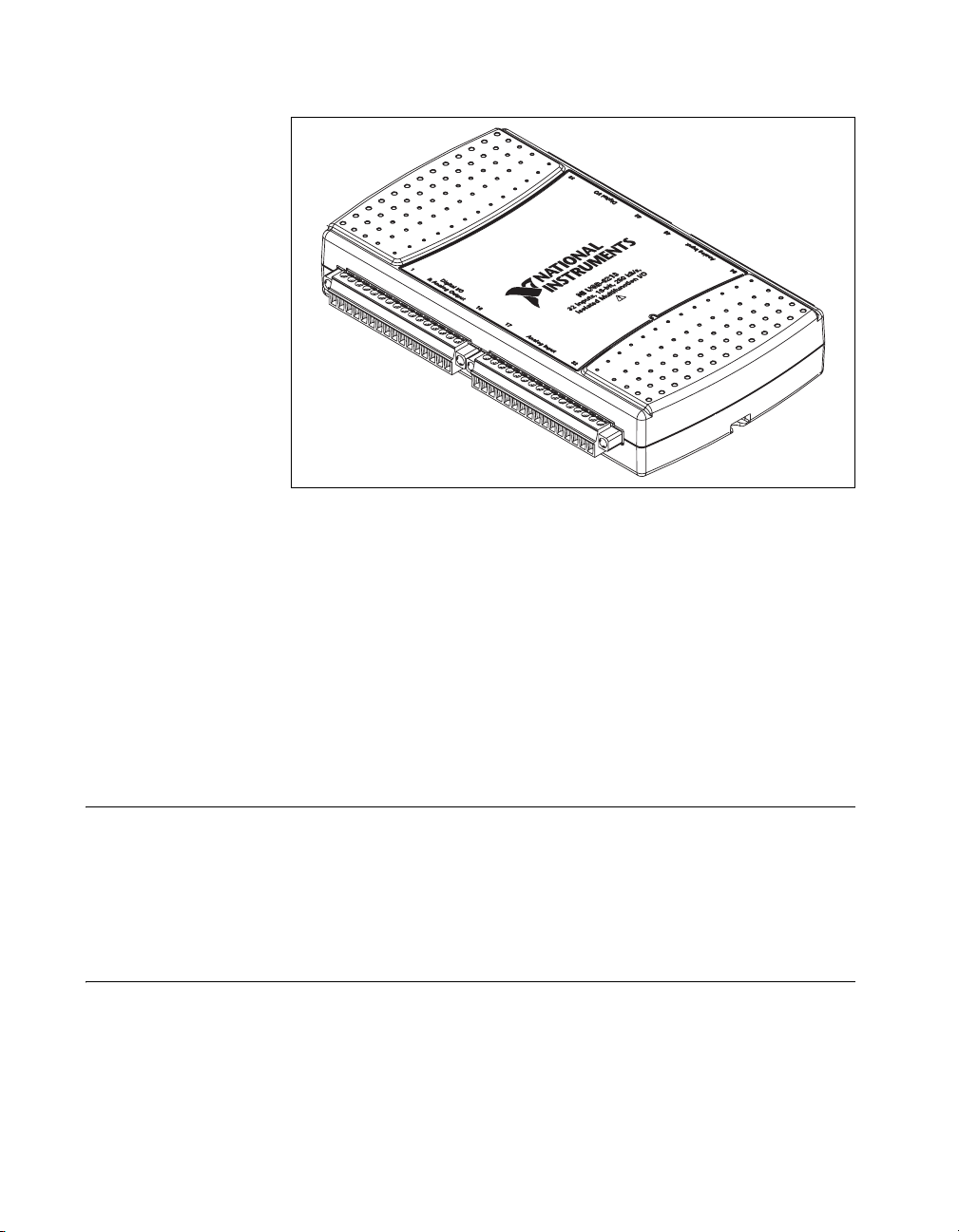
Figure 1-2. USB-6215/6218
NI 621x devices feature up to 32 analog input (AI) channels, up to two
analog output (AO) channels, 8 lines of digital input (DI), 8 lines of digital
output (DO), and two counters. If you have not already installed your
device, refer to the NI-DAQmx for USB Devices Getting Started Guide. For
specifications, refer to the NI 621x Specifications document on
ni.com/manuals.
Before installing your DAQ device, you must install the software you plan
to use with the device.
Installing NI-DAQmx
The NI-DAQmx for USB Devices Getting Started Guide, which you can
download at
instructions for installing software and hardware, configuring channels and
tasks, and getting started developing an application.
ni.com/manuals, offers NI-DAQmx users step-by-step
Installing Other Software
If you are using other software, refer to the installation instructions that
accompany your software.
NI USB-621x User Manual 1-2 ni.com
Page 19

Installing the Hardware
The NI-DAQmx for USB Devices Getting Started Guide contains
non-software-specific information about how to install USB devices.
Device Pinouts
Refer to Appendix A, Device-Specific Information, for NI 621x device
pinouts.
Device Specifications
Refer to the NI 621x Specifications, available on the NI-DAQ Device
Document Browser or
about NI 621x devices.
Device Accessories
NI offers a variety of accessories to use with your DAQ device. Refer to
Appendix A, Device-Specific Information, or
information.
Chapter 1 Getting Started
ni.com/manuals, for more detailed information
ni.com for more
© National Instruments Corporation 1-3 NI USB-621x User Manual
Page 20
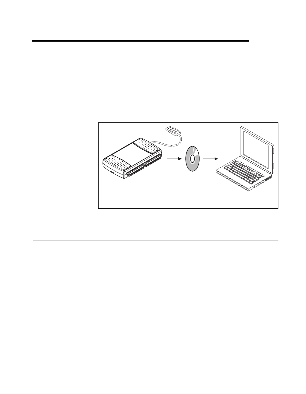
DAQ System Overview
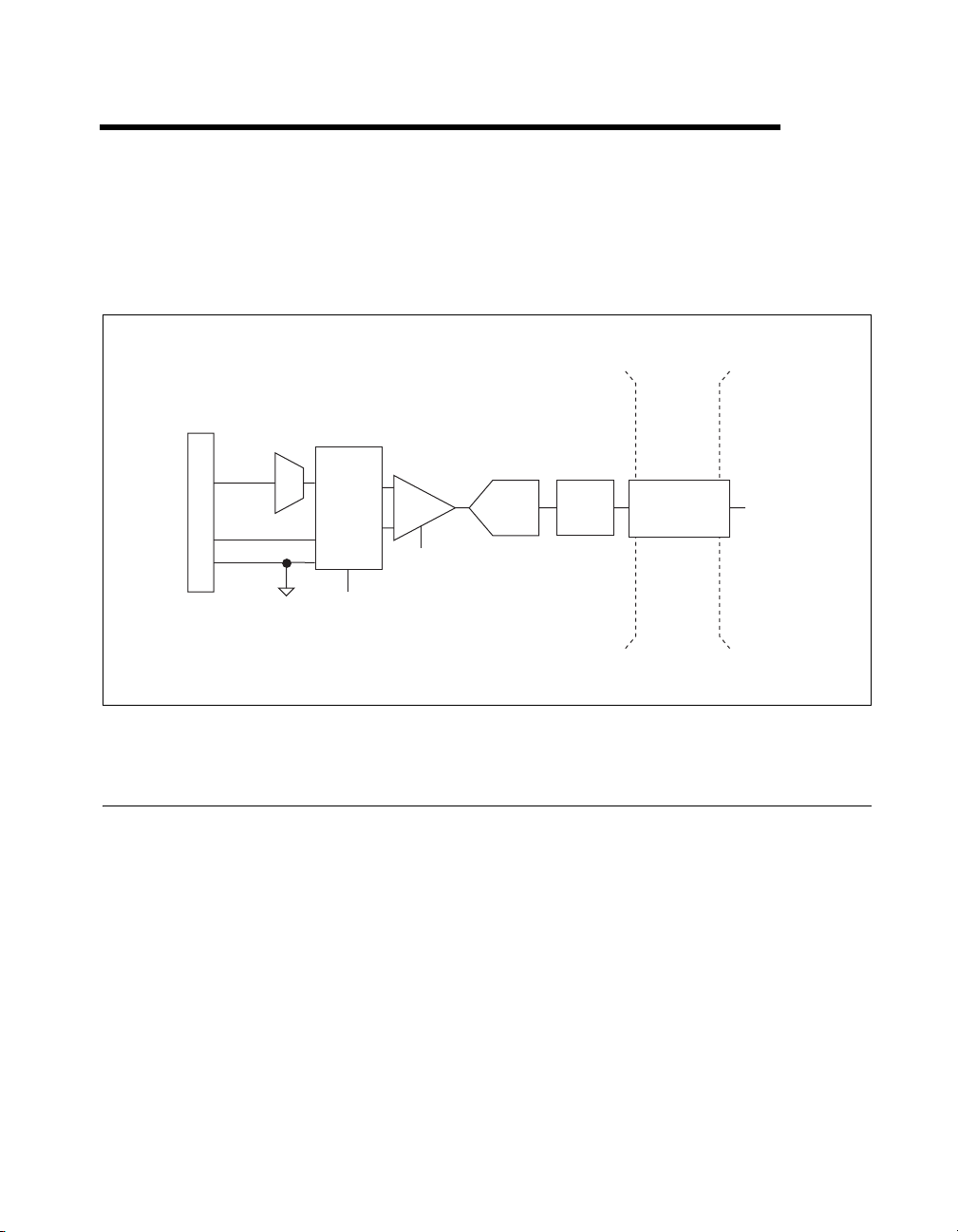
Figure 2-1 shows a typical DAQ system, which includes sensors,
transducers, signal conditioning devices, cables that connect the various
devices to the accessories, the M Series device, programming software, and
PC. The following sections cover the components of a typical DAQ system.
2
DAQ Hardware
DAQ
Hardware
Figure 2-1. Components of a Typical DAQ System
DAQ hardware digitizes signals, performs D/A conversions to generate
analog output signals, and measures and controls digital I/O signals.
Figure 2-2 features components common to all USB M Series devices.
DAQ
Software
Personal Computer
or Laptop
© National Instruments Corporation 2-1 NI USB-621x User Manual
Page 21
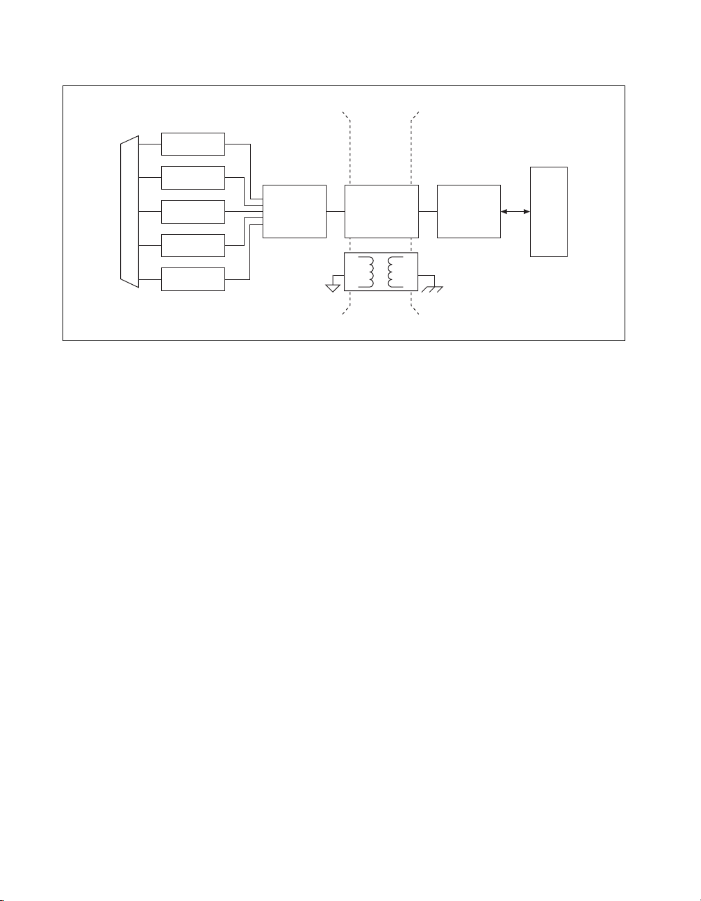
Chapter 2 DAQ System Overview
Analog Input
Analog Output
Digital I/O
I/O Connector
Counters
PFI
DAQ-STC2
The DAQ-STC2 implements a high-performance digital engine for
M Series data acquisition hardware. Some key features of this engine
include the following:
• Flexible AI and AO sample and convert timing
• Many triggering modes
• Independent AI, AO, and CTR FIFOs
• Generation and routing of internal and external timing signals
• Two flexible 32-bit counter/timer modules with hardware gating
• Static DI and static DO signals
• USB Hi-Speed 2.0 interface
• Up to four USB Signal Streams for acquisition and generation
and Clock
Generation
functions
Digital
Routing
Isolation
Barrier
(USB-6215
and USB-6218
devices only)
Digital
Isolators
Bus
Interface
Figure 2-2. USB-621x Block Diagram
Bus
Calibration Circuitry
The M Series analog inputs and outputs have calibration circuitry to correct
gain and offset errors. You can calibrate the device to minimize AI and AO
errors caused by time and temperature drift at run time. No external
circuitry is necessary; an internal reference ensures high accuracy and
stability over time and temperature changes.
NI USB-621x User Manual 2-2 ni.com
Page 22

Factory-calibration constants are permanently stored in an onboard
EEPROM and cannot be modified. When you self-calibrate the device,
software stores new constants in a user-modifiable section of the EEPROM.
To return a device to its initial factory calibration settings, software can
copy the factory-calibration constants to the user-modifiable section of the
EEPROM. Refer to the NI-DAQmx Help or the LabVIEW 8.x Help for more
information about using calibration constants.
Signal Conditioning
Many sensors and transducers require signal conditioning before a
measurement system can effectively and accurately acquire the signal. The
front-end signal conditioning system can include functions such as signal
amplification, attenuation, filtering, electrical isolation, simultaneous
sampling, and multiplexing. In addition, many transducers require
excitation currents or voltages, bridge completion, linearization, or high
amplification for proper and accurate operation. Therefore, most
computer-based measurement systems include some form of signal
conditioning in addition to plug-in data acquisition DAQ devices.
Sensors and Transducers
Sensors can generate electrical signals to measure physical phenomena,
such as temperature, force, sound, or light. Some commonly used sensors
are strain gauges, thermocouples, thermistors, angular encoders, linear
encoders, and resistance temperature detectors (RTDs).
Chapter 2 DAQ System Overview
To measure signals from these various transducers, you must convert them
into a form that a DAQ device can accept. For example, the output voltage
of most thermocouples is very small and susceptible to noise. Therefore,
you may need to amplify or filter the thermocouple output before digitizing
it. The manipulation of signals to prepare them for digitizing is called
signal conditioning.
For more information about sensors, refer to the following documents.
• For general information about sensors, visit
• If you are using LabVIEW, refer to the LabVIEW Help by selecting
Help»Search the LabVIEW Help in LabVIEW and then navigate to
the Taking Measurements book on the Contents tab.
• If you are using other application software, refer to Common Sensors
in the NI-DAQmx Help or the LabVIEW 8.x Help.
© National Instruments Corporation 2-3 NI USB-621x User Manual
ni.com/sensors.
Page 23

Chapter 2 DAQ System Overview
Programming Devices in Software
National Instruments measurement devices are packaged with NI-DAQ
driver software, an extensive library of functions and VIs you can call from
your application software, such as LabVIEW or LabWindows/CVI, to
program all the features of your NI measurement devices. Driver software
has an application programming interface (API), which is a library of VIs,
functions, classes, attributes, and properties for creating applications for
your device.
NI-DAQ 7.3 and later includes two NI-DAQ drivers—Traditional NI-DAQ
(Legacy) and NI-DAQmx. M Series devices use the NI-DAQmx driver.
Each driver has its own API, hardware configuration, and software
configuration. Refer to the NI-DAQmx for USB Devices Getting Started
Guide for more information about the two drivers.
NI-DAQmx includes a collection of programming examples to help you get
started developing an application. You can modify example code and save
it in an application. You can use examples to develop a new application or
add example code to an existing application.
To locate LabVIEW and LabWindows/CVI examples, open the National
Instruments Example Finder.
• In LabVIEW, select Help»Find Examples.
• In LabWindows/CVI, select Help»NI Example Finder.
Measurement Studio, Visual Basic, and ANSI C examples are located in the
following directories:
• NI-DAQmx examples for Measurement Studio-supported languages
are in the following directories:
–
MeasurementStudio\VCNET\Examples\NIDaq
– MeasurementStudio\DotNET\Examples\NIDaq
• NI-DAQmx examples for ANSI C are in the
NI-DAQ\Examples\DAQmx ANSI C Dev directory
For additional examples, refer to
NI USB-621x User Manual 2-4 ni.com
zone.ni.com.
Page 24

3
Connector Information
The I/O Connector Signal Descriptions and +5 V Power sections contain
information about NI 621x connectors. Refer to Appendix A,
Device-Specific Information, for device I/O connector pinouts.
I/O Connector Signal Descriptions
Table 3-1 describes the signals found on the I/O connectors. Not all signals
are available on all devices.
Table 3-1. I/O Connector Signals
Signal Name Reference Direction Description
AI GND — — Analog Input Ground—These terminals are the
reference point for single-ended AI measurements in
RSE mode and the bias current return point for DIFF
measurements. All three ground references—AI GND,
AO GND, and D GND—are connected on the device.
AI <0..31> Va r ie s Input Analog Input Channels 0 to 31—For single-ended
measurements, each signal is an analog input voltage
channel. In RSE mode, AI GND is the reference for these
signals. In NRSE mode, the reference for each
AI <0..31> signal is AI SENSE.
For differential measurements, AI 0 and AI 8 are the
positive and negative inputs of differential analog input
channel 0. Similarly, the following signal pairs also form
differential input channels:
<AI 1, AI 9>, <AI 2, AI 10>, <AI 3, AI 11>,
<AI4,AI12>, <AI5,AI13>, <AI6,AI14>,
<AI 7, AI 15>, <AI 16, AI 24>, <AI 17, AI 25>,
<AI 18, AI 26>, <AI 19, AI 27>, <AI 20, AI 28>,
<AI 21, AI 29>, <AI 22, AI 30>, <AI 23, AI 31>
AI SENSE — Input Analog Input Sense—In NRSE mode, the reference for
each AI <0..31> signal is AI SENSE.
AO <0..1> AO GND Output Analog Output Channels 0 to 1—These terminals
supply the voltage output of AO channels 0 to 1.
© National Instruments Corporation 3-1 NI USB-621x User Manual
Page 25

Chapter 3 Connector Information
Table 3-1. I/O Connector Signals (Continued)
Signal Name Reference Direction Description
AO GND — — Analog Output Ground—AO GND is the reference for
AO <0..1>. All three ground references—AI GND,
AO GND, and D GND—are connected on the device.
D GND — — Digital Ground—D GND supplies the reference for
PFI <0..15>/P0/P1 and +5 V. All three ground
references—AI GND, AO GND, and D GND—are
connected on the device.
+5 V D GND Input or
Output
PFI <0..3>,
PFI <8..11>/P0.<0..7>
PFI <4..7>,
PFI <12..15>/P1.<0..7>
NC — — No connect—Do not connect signals to these terminals.
D GND Input Programmable Function Interface or Static Digital
D GND Output Programmable Function Interface or Static Digital
+5 V Power—These terminals provide a +5 V power
source or can be used to externally power the PFI outputs.
Input Channels 0 to 7—Each PFI terminal can be used
to supply an external source for AI, AO, or counter/timer
inputs.
You also can use these terminals as static digital input
lines.
Output Channels 0 to 7—You can route many different
internal AI, AO, or counter/timer outputs to each PFI
terminal.
You also can use these terminals as static digital output
lines.
+5 V Power
The +5 V terminals on the I/O connector can be use as either an output or
an input. Both terminals are internally connected on the USB-621x.
+5 V Power as an Output
Because the USB-621x devices are bus powered, there is a 50 mA limit on
the total current that can be drawn from the +5 V terminals and the digital
outputs PFI <4..7> and PFI <12..15>/P1.<0..7>. The USB-621x monitors
the total current and will drop the voltage on all of the digital outputs and
the +5 V terminals if the 50 mA limit is exceeded.
NI USB-621x User Manual 3-2 ni.com
Page 26

+5 V Power as an Input
If you have high current loads for the digital outputs to drive, you can
exceed the 50 mA internal limit by connecting an external +5 V power
source to the +5 V terminals. These terminals are protected against
undervoltage and overvoltage, and they have a 350 mA self-resetting fuse
to protect them from short circuit conditions. If your USB-621x device has
more than one +5 V terminal, you can connect the external power supply to
one terminal and use the other as a power source.
Chapter 3 Connector Information
© National Instruments Corporation 3-3 NI USB-621x User Manual
Page 27
Analog Input
Figure 4-1 shows the analog input circuitry of NI 621x devices.
AI <0..n>
MUX
DIFF, RSE,
AI SENSE
I/O Connector
AI GND
AI Terminal
Configuration
or NRSE
Selection
NI-PGIA
Input Range
Selection
ADC
AI FIFO
Isolation
Barrier
(USB-6215
and USB-6218
devices only)
Digital
Isolators
4
AI Data
Figure 4-1. M Series Analog Input Circuitry
Analog Input Circuitry
I/O Connector
You can connect analog input signals to the M Series device through the I/O
connector. The proper way to connect analog input signals depends on the
analog input ground-reference settings, described in the Analog Input
Ground-Reference Settings section. Also refer to Appendix A,
Device-Specific Information, for device I/O connector pinouts.
MUX
Each M Series device has one analog-to-digital converter (ADC). The
multiplexers (MUX) route one AI channel at a time to the ADC through the
NI-PGIA.
© National Instruments Corporation 4-1 NI USB-621x User Manual
Page 28

Chapter 4 Analog Input
Ground-Reference Settings
The analog input ground-reference settings circuitry selects between
differential, referenced single-ended, and non-referenced single-ended
input modes. Each AI channel can use a different mode.
Instrumentation Amplifier (NI-PGIA)
The NI programmable gain instrumentation amplifier (NI-PGIA) is a
measurement and instrument class amplifier that minimizes settling times
for all input ranges. The NI-PGIA can amplify or attenuate an AI signal to
ensure that you use the maximum resolution of the ADC.
M Series devices use the NI-PGIA to deliver high accuracy even when
sampling multiple channels with small input ranges at fast rates. M Series
devices can sample channels in any order at the maximum conversion rate,
and you can individually program each channel in a sample with a different
input range.
A/D Converter
The analog-to-digital converter (ADC) digitizes the AI signal by converting
the analog voltage into a digital number.
AI FIFO
M Series devices can perform both single and multiple A/D conversions of
a fixed or infinite number of samples. A large first-in-first-out (FIFO)
buffer holds data during AI acquisitions to ensure that no data is lost.
M Series devices can handle multiple A/D conversion operations with
DMA, interrupts, or programmed I/O.
Analog Input Range
The input range affects the resolution of the M Series device for an AI
channel. For example, a 16-bit ADC converts analog inputs into one of
65,536 (= 2
an input range of –10 V to 10 V, the voltage of each code of a 16-bit ADC
is:
M Series devices use a calibration method that requires some codes
(typically about 5% of the codes) to lie outside of the specified range. This
NI USB-621x User Manual 4-2 ni.com
16
) codes—that is, one of 65,536 possible digital values. So, for
(10 V – (–10 V))
16
2
= 305 μV
Page 29

Chapter 4 Analog Input
calibration method improves absolute accuracy, but it increases the nominal
resolution of input ranges by about 5% over what the formula shown above
would indicate.
Choose an input range that matches the expected input range of your signal.
A large input range can accommodate a large signal variation, but reduces
the voltage resolution. Choosing a smaller input range improves the voltage
resolution, but may result in the input signal going out of range.
For more information about setting ranges, refer to the NI-DAQmx Help or
the LabVIEW 8.x Help.
Table 4-1 shows the input ranges and resolutions supported by NI 621x
devices.
Table 4-1. Input Ranges for NI 621x
Nominal Resolution Assuming
Input Range
–10 V to 10 V 320 μV
–5 V to 5 V 160 μV
5% Over Range
–1 V to 1 V 32 μV
–200 mV to 200 mV 6.4 μV
Analog Input Ground-Reference Settings
NI 621x devices support the analog input ground-reference settings shown
in Table 4-2.
Table 4-2. Analog Input Ground-Reference Settings
AI Ground-Reference
Settings
DIFF In differential (DIFF) mode, NI 621x devices measure the difference in
voltage between two AI signals.
RSE In referenced single-ended (RSE) mode, NI 621x devices measure the
voltage of an AI signal relative to AI GND.
NRSE In non-referenced single-ended (NRSE) mode, NI 621x devices measure
the voltage of an AI signal relative to the AI SENSE input.
Description
© National Instruments Corporation 4-3 NI USB-621x User Manual
Page 30
Chapter 4 Analog Input
The AI ground-reference setting determines how you should connect your
AI signals to the NI 621x device. Refer to Chapter 5, Connecting AI Signals
on the USB-6210/6211 Devices, section for more information.
Ground-reference settings are programmed on a per-channel basis. For
example, you might configure the device to scan 12 channels—four
differentially-configured channels and eight single-ended channels.
NI 621x devices implement the different analog input ground-reference
settings by routing different signals to the NI-PGIA. The NI-PGIA is a
differential amplifier. That is, the NI-PGIA amplifies (or attenuates) the
difference in voltage between its two inputs. The NI-PGIA drives the ADC
with this amplified voltage. The amount of amplification (the gain), is
determined by the analog input range, as shown in Figure 4-2.
Instrumentation
V
in+
Amplifier
AI Ground-Reference
Settings
RSE AI <0..31> AI GND
NRSE AI <0..31> AI SENSE
DIFF AI <0..7> AI <8..15>
V
m
] × Gain
+
Measured
Voltage
–
PGIA
V
in–
Vm = [V
in+
– V
in–
Figure 4-2. NI-PGIA
Table 4-3 shows how signals are routed to the NI-PGIA.
Table 4-3. Signals Routed to the NI-PGIA
Signals Routed to the Positive
Input of the NI-PGIA (V
in+
Signals Routed to the Negative
)
Input of the NI-PGIA (V
in–
)
AI <16..23> AI <24..31>
For differential measurements, AI 0 and AI 8 are the positive and negative
inputs of differential analog input channel 0. For a complete list of signal
NI USB-621x User Manual 4-4 ni.com
Page 31

pairs that form differential input channels, refer to the I/O Connector Signal
Descriptions section of Chapter 3, Connector Information.
Caution The maximum input voltages rating of AI signals with respect to AI GND (and
for differential signals with respect to each other) are listed in the specifications document
for your device. Exceeding the maximum input voltage of AI signals distorts the
measurement results. Exceeding the maximum input voltage rating also can damage the
device and the computer. NI is not liable for any damage resulting from such signal
connections.
AI ground-reference setting is sometimes referred to as AI terminal
configuration.
Configuring AI Ground-Reference Settings in Software
You can program channels on an M Series device to acquire with different
ground references.
Chapter 4 Analog Input
To enable multimode scanning in LabVIEW, use
Virtual Channel.vi
of the NI-DAQmx API. You must use a new VI for
NI-DAQmx Create
each channel or group of channels configured in a different input mode. In
Figure 4-3, channel 0 is configured in differential mode, and channel 1 is
configured in RSE mode.
Figure 4-3. Enabling Multimode Scanning in LabVIEW
To configure the input mode of your voltage measurement using the DAQ
Assistant, use the Terminal Configuration drop-down list. Refer to the
DAQ Assistant Help for more information about the DAQ Assistant.
To configure the input mode of your voltage measurement using the
NI-DAQmx C API, set the terminalConfig property. Refer to the
NI-DAQmx C Reference Help for more information.
© National Instruments Corporation 4-5 NI USB-621x User Manual
Page 32

Chapter 4 Analog Input
Multichannel Scanning Considerations
M Series devices can scan multiple channels at high rates and digitize the
signals accurately. However, you should consider several issues when
designing your measurement system to ensure the high accuracy of your
measurements.
In multichannel scanning applications, accuracy is affected by settling
time. When your NI 621x device switches from one AI channel to another
AI channel, the device configures the NI-PGIA with the input range of the
new channel. The NI-PGIA then amplifies the input signal with the gain for
the new input range. Settling time refers to the time it takes the NI-PGIA to
amplify the input signal to the desired accuracy before it is sampled by the
ADC. The specifications document for your DAQ device lists its settling
time.
NI 621x devices are designed to have fast settling times. However, several
factors can increase the settling time which decreases the accuracy of your
measurements. To ensure fast settling times, you should do the following
(in order of importance):
• Use low impedance sources
• Use short high-quality cabling
• Carefully choose the channel scanning order
• Avoid scanning faster than necessary
The following sections contain more information about these factors.
Use Low Impedance Sources
To ensure fast settling times, your signal sources should have an impedance
of <1 kΩ. Large source impedances increase the settling time of the
NI-PGIA, and so decrease the accuracy at fast scanning rates.
Settling times increase when scanning high-impedance signals due to a
phenomenon called charge injection. Multiplexers contain switches,
usually made of switched capacitors. When one of the channels, for
example channel 0, is selected in a multiplexer, those capacitors
accumulate charge. When the next channel, for example channel 1, is
selected, the accumulated charge leaks backward through channel 1. If the
output impedance of the source connected to channel 1 is high enough, the
resulting reading of channel 1 can be partially affected by the voltage on
channel 0. This effect is referred to as ghosting.
NI USB-621x User Manual 4-6 ni.com
Page 33

If your source impedance is high, you can decrease the scan rate to allow
the NI-PGIA more time to settle. Another option is to use a voltage follower
circuit external to your DAQ device to decrease the impedance seen by the
DAQ device. Refer to the KnowledgeBase document, How Do I Create a
Buffer to Decrease the Source Impedance of My Analog Input Signal?,
by going to
ni.com/info and entering the info code rdbbis.
Carefully Choose the Channel Scanning Order
Avoid Switching from a Large to a Small Input Range
Switching from a channel with a large input range to a channel with a small
input range can greatly increase the settling time.
Suppose a 4 V signal is connected to channel 0 and a 1 mV signal is
connected to channel 1. The input range for channel 0 is –10 V to 10 V and
the input range of channel 1 is –200 mV to 200 mV.
When the multiplexer switches from channel 0 to channel 1, the input to the
NI-PGIA switches from 4 V to 1 mV. The approximately 4 V step from 4 V
to 1 mV is 1,000% of the new full-scale range. For a 16-bit device to settle
within 0.0015% (15 ppm or 1 LSB) of the ±200 mV full-scale range on
channel 1, the input circuitry must settle to within 0.000031% (0.31 ppm or
1/50 LSB) of the ±10 V range. Some devices can take many microseconds
for the circuitry to settle this much.
Chapter 4 Analog Input
To avoid this effect, you should arrange your channel scanning order so that
transitions from large to small input ranges are infrequent.
In general, you do not need this extra settling time when the NI-PGIA is
switching from a small input range to a larger input range.
Insert Grounded Channel between Signal Channels
Another technique to improve settling time is to connect an input channel
to ground. Then insert this channel in the scan list between two of your
signal channels. The input range of the grounded channel should match the
input range of the signal after the grounded channel in the scan list.
Consider again the example above where a 4 V signal is connected to
channel 0 and a 1 mV signal is connected to channel 1. Suppose the input
range for channel 0 is –10 V to 10 V and the input range of channel 1 is
–200mV to 200mV.
© National Instruments Corporation 4-7 NI USB-621x User Manual
Page 34

Chapter 4 Analog Input
You can connect channel 2 to AI GND (or you can use the internal ground
signal; refer to Internal Channels in the NI-DAQmx Help). Set the input
range of channel 2 to –200 mV to 200 mV to match channel 1. Then scan
channels in the order: 0, 2, 1.
Inserting a grounded channel between signal channels improves settling
time because the NI-PGIA adjusts to the new input range setting faster
when the input is grounded.
Minimize Voltage Step between Adjacent Channels
When scanning between channels that have the same input range, the
settling time increases with the voltage step between the channels. If you
know the expected input range of your signals, you can group signals with
similar expected ranges together in your scan list.
For example, suppose all channels in a system use a –5 to 5 V input range.
The signals on channels 0, 2, and 4 vary between 4.3 V and 5 V. The signals
on channels 1, 3, and 5 vary between –4 V and 0 V. Scanning channels in
the order 0, 2, 4, 1, 3, 5 produces more accurate results than scanning
channels in the order 0, 1, 2, 3, 4, 5.
Avoid Scanning Faster Than Necessary
Designing your system to scan at slower speeds gives the NI-PGIA more
time to settle to a more accurate level. Here are two examples to consider.
Example 1
Averaging many AI samples can increase the accuracy of the reading by
decreasing noise effects. In general, the more points you average, the more
accurate the final result. However, you may choose to decrease the number
of points you average and slow down the scanning rate.
Suppose you want to sample 10 channels over a period of 20 ms and
average the results. You could acquire 250 points from each channel at a
scan rate of 125 kS/s. Another method would be to acquire 500 points from
each channel at a scan rate of 250 kS/s. Both methods take the same amount
of time. Doubling the number of samples averaged (from 250 to 500)
decreases the effect of noise by a factor of 1.4 (the square root of 2).
However, doubling the number of samples (in this example) decreases the
time the NI-PGIA has to settle from 8 µs to 4 µs. In some cases, the slower
scan rate system returns more accurate results.
NI USB-621x User Manual 4-8 ni.com
Page 35

Example 2
If the time relationship between channels is not critical, you can sample
from the same channel multiple times and scan less frequently. For
example, suppose an application requires averaging 100 points from
channel 0 and averaging 100 points from channel 1. You could alternate
reading between channels—that is, read one point from channel 0, then
one point from channel 1, and so on. You also could read all 100 points
from channel 0 then read 100 points from channel 1. The second method
switches between channels much less often and is affected much less by
settling time.
Analog Input Data Acquisition Methods
When performing analog input measurements, you either can perform
software-timed or hardware-timed acquisitions. Hardware-timed
acquisitions can be buffered or non-buffered.
Software-Timed Acquisitions
With a software-timed acquisition, software controls the rate of the
acquisition. Software sends a separate command to the hardware to initiate
each ADC conversion. In NI-DAQmx, software-timed acquisitions are
referred to as having on-demand timing. Software-timed acquisitions are
also referred to as immediate or static acquisitions and are typically used
for reading a single sample of data.
Chapter 4 Analog Input
Hardware-Timed Acquisitions
With hardware-timed acquisitions, a digital hardware signal
(ai/SampleClock) controls the rate of the acquisition. This signal can be
generated internally on your device or provided externally.
Hardware-timed acquisitions have several advantages over software-timed
acquisitions.
• The time between samples can be much shorter.
• The timing between samples is deterministic.
• Hardware-timed acquisitions can use hardware triggering.
Hardware-timed operations can be buffered or non-buffered.
© National Instruments Corporation 4-9 NI USB-621x User Manual
Page 36

Chapter 4 Analog Input
Buffered
In a buffered acquisition, data is moved from the DAQ device’s onboard
FI FO memory to a PC bu ffer u s ing USB signal streams or programmed I/O
before it is transferred to application memory. Buffered acquisitions
typically allow for much faster transfer rates than non-buffered acquisitions
because data is moved in large blocks, rather than one point at a time.
One property of buffered I/O operations is the sample mode. The sample
mode can be either finite or continuous.
Finite sample mode acquisition refers to the acquisition of a specific,
predetermined number of data samples. Once the specified number of
samples has been written out, the generation stops. If you use a reference
trigger, you must use finite sample mode.
Continuous acquisition refers to the acquisition of an unspecified number
of samples. Instead of acquiring a set number of data samples and stopping,
a continuous acquisition continues until you stop the operation. Continuous
acquisition is also referred to as double-buffered or circular-buffered
acquisition.
If data cannot be transferred across the bus fast enough, the FIFO becomes
full. New acquisitions will overwrite data in the FIFO before it can be
transferred to host memory. The device generates an error in this case. With
continuous operations, if the user program does not read data out of the PC
buffer fast enough to keep up with the data transfer, the buffer could reach
an overflow condition, causing an error to be generated.
Non-Buffered
Hardware-timed, non-buffered mode is not supported for USB M series
devices.
Analog Input Digital Triggering
Analog input supports three different triggering actions:
• Start trigger
• Reference trigger
• Pause trigger
Refer to the AI Start Trigger Signal, AI Reference Trigger Signal, and AI
Pause Trigger Signal sections for information about these triggers.
NI USB-621x User Manual 4-10 ni.com
Page 37

A digital trigger can initiate these actions. All NI 621x devices support
digital triggering. NI 621x devices do not support analog triggering.
Field Wiring Considerations
Environmental noise can seriously affect the measurement accuracy of the
device if you do not take proper care when running signal wires between
signal sources and the device. The following recommendations apply
mainly to AI signal routing to the device, although they also apply to signal
routing in general.
Minimize noise pickup and maximize measurement accuracy by taking the
following precautions.
• Use DIFF AI connections to reject common-mode noise.
• Use individually shielded, twisted-pair wires to connect AI signals to
the device. With this type of wire, the signals attached to the positive
and negative input channels are twisted together and then covered with
a shield. You then connect this shield only at one point to the signal
source ground. This kind of connection is required for signals traveling
through areas with large magnetic fields or high electromagnetic
interference.
Chapter 4 Analog Input
Refer to the NI Developer Zone document, Field Wiring and Noise
Considerations for Analog Signals, for more information. To access this
document, go to
ni.com/info and enter the info code rdfwn3.
Analog Input Timing Signals
In order to provide all of the timing functionality described throughout this
section, M Series devices have a flexible timing engine. Figure 4-4
summarizes all of the timing options provided by the analog input timing
engine.
© National Instruments Corporation 4-11 NI USB-621x User Manual
Page 38

Chapter 4 Analog Input
20 MHz Timebase
100 kHz Timebase
ai/SampleClock
Timebase
Analog Comparison Event
Ctr
n
Internal Output
SW Pulse
Programmable
Clock
Divider
ai/SampleClock
ai/ConvertClock
ai/ConvertClock
Timebase
n
Internal Output
Ctr
Programmable
Clock
Divider
Figure 4-4. Analog Input Timing Options
M Series devices use ai/SampleClock and ai/ConvertClock to perform
interval sampling. As Figure 4-5 shows, ai/SampleClock controls the
sample period, which is determined by the following equation:
1/Sample Period = Sample Rate
Channel 0
Channel 1
Convert Period
Sample Period
Figure 4-5. Interval Sampling
ai/ConvertClock controls the Convert Period, which is determined by the
following equation:
1/Convert Period = Convert Rate
NI USB-621x User Manual 4-12 ni.com
Page 39

Chapter 4 Analog Input
NI-DAQmx chooses the default convert rate to allow for the maximum
settling time between conversions. Typically, this rate is the sampling rate
for the task multiplied by the number of channels in the task.
Note The sampling rate is the fastest you can acquire data on the device and still achieve
accurate results. For example, if an M Series device has a sampling rate of 250 kS/s, this
sampling rate is aggregate—one channel at 250 kS/s or two channels at 125 kS/s per
channel illustrates the relationship.
Posttriggered data acquisition allows you to view only data that is acquired
after a trigger event is received. A typical posttriggered DAQ sequence is
shown in Figure 4-6. The sample counter is loaded with the specified
number of posttrigger samples, in this example, five. The value decrements
with each pulse on ai/SampleClock, until the value reaches zero and all
desired samples have been acquired.
ai/StartTrigger
ai/SampleClock
ai/ConvertClock
Sample Counter
Figure 4-6. Posttriggered Data Acquisition Example
13042
Pretriggered data acquisition allows you to view data that is acquired before
the trigger of interest, in addition to data acquired after the trigger.
Figure 4-7 shows a typical pretriggered DAQ sequence. ai/StartTrigger can
be either a hardware or software signal. If ai/StartTrigger is set up to be a
software start trigger, an output pulse appears on the ai/StartTrigger line
when the acquisition begins. When the ai/StartTrigger pulse occurs, the
sample counter is loaded with the number of pretriggered samples, in this
example, four. The value decrements with each pulse on ai/SampleClock,
until the value reaches zero. The sample counter is then loaded with the
number of posttriggered samples, in this example, three.
© National Instruments Corporation 4-13 NI USB-621x User Manual
Page 40

Chapter 4 Analog Input
ai/StartTrigger
ai/ReferenceTrigger
ai/SampleClock
ai/ConvertClock
Scan Counter
Figure 4-7. Pretriggered Data Acquisition Example
n/a
3
0 1 2
1 0 2 2 2
If an ai/ReferenceTrigger pulse occurs before the specified number of
pretrigger samples are acquired, the trigger pulse is ignored. Otherwise,
when the ai/ReferenceTrigger pulse occurs, the sample counter value
decrements until the specified number of posttrigger samples have been
acquired.
USB M Series devices feature the following analog input timing signals.
• AI Sample Clock Signal
• AI Sample Clock Timebase Signal
• AI Convert Clock Signal
• AI Convert Clock Timebase Signal
• AI Hold Complete Event Signal
• AI Start Trigger Signal
• AI Reference Trigger Signal
• AI Pause Trigger Signal
AI Sample Clock Signal
Use the AI Sample Clock (ai/SampleClock) signal to initiate a set of
measurements. Your M Series device samples the AI signals of every
channel in the task once for every ai/SampleClock. A measurement
acquisition consists of one or more samples.
You can specify an internal or external source for ai/SampleClock. You also
can specify whether the measurement sample begins on the rising edge or
falling edge of ai/SampleClock.
NI USB-621x User Manual 4-14 ni.com
Page 41

Chapter 4 Analog Input
Using an Internal Source
One of the following internal signals can drive ai/SampleClock.
• Counter n Internal Output
• AI Sample Clock Timebase (divided down)
•A software pulse
A programmable internal counter divides down the sample clock timebase.
Using an External Source
Use the external signals PFI <0..3> or PFI <8..11> as the source of
ai/SampleClock.
Routing AI Sample Clock Signal to an Output Terminal
You can route ai/SampleClock out to any PFI <4..7> or PFI <12..15>
terminal. This pulse is always active high.
You can specify the output to have one of two behaviors. With the pulse
behavior, your DAQ device briefly pulses the PFI terminal once for every
occurrence of ai/SampleClock.
With level behavior, your DAQ device drives the PFI terminal high during
the entire sample.
Other Timing Requirements
Your DAQ device only acquires data during an acquisition. The device
ignores ai/SampleClock when a measurement acquisition is not in progress.
During a measurement acquisition, you can cause your DAQ device to
ignore ai/SampleClock using the ai/PauseTrigger signal.
A counter on your device internally generates ai/SampleClock unless you
select some external source. ai/StartTrigger starts this counter and either
software or hardware can stop it once a finite acquisition completes. When
using an internally generated ai/SampleClock, you also can specify a
configurable delay from ai/StartTrigger to the first ai/SampleClock pulse.
By default, this delay is set to two ticks of the ai/SampleClockTimebase
signal. When using an externally generated ai/SampleClock, you must
ensure the clock signal is consistent with respect to the timing requirements
of ai/ConvertClock. Failure to do so may result in ai/SampleClock pulses
that are masked off and acquisitions with erratic sampling intervals. Refer
© National Instruments Corporation 4-15 NI USB-621x User Manual
Page 42

Chapter 4 Analog Input
to AI Convert Clock Signal for more information about the timing
requirements between ai/ConvertClock and ai/SampleClock.
Figure 4-8 shows the relationship of ai/SampleClock to ai/StartTrigger.
ai/SampleClockTimebase
Figure 4-8. ai/SampleClock and ai/StartTrigger
AI Sample Clock Timebase Signal
You can route any of the following signals to be the AI Sample Clock
Timebase (ai/SampleClockTimebase) signal:
• 20 MHz Timebase
• 100 kHz Timebase
• PFI <0..3>, PFI <8..11>
ai/StartTrigger
ai/SampleClock
Delay
From
Start
Trigger
ai/SampleClockTimebase is not available as an output on the I/O connector.
ai/SampleClockTimebase is divided down to provide one of the possible
sources for ai/SampleClock. You can configure the polarity selection for
ai/SampleClockTimebase as either rising or falling edge.
AI Convert Clock Signal
Use the AI Convert Clock (ai/ConvertClock) signal to initiate a single A/D
conversion on a single channel. A sample (controlled by the AI Sample
Clock) consists of one or more conversions.
You can specify either an internal or external signal as the source of
ai/ConvertClock. You also can specify whether the measurement sample
begins on the rising edge or falling edge of ai/ConvertClock.
By default, NI-DAQmx chooses the fastest conversion rate possible based
on the speed of the A/D converter and adds 10 µs of padding between each
NI USB-621x User Manual 4-16 ni.com
Page 43

Chapter 4 Analog Input
channel to allow for adequate settling time. This scheme enables the
channels to approximate simultaneous sampling and still allow for
adequate settling time. If the AI Sample Clock rate is too fast to allow for
this 10 µs of padding, NI-DAQmx chooses the conversion rate so that the
AI Convert Clock pulses are evenly spaced throughout the sample.
To explicitly specify the conversion rate, use AI Convert Clock Rate
DAQmx Timing property node or function.
Caution Setting the conversion rate higher than the maximum rate specified for your
device will result in errors.
Using an Internal Source
One of the following internal signals can drive ai/ConvertClock:
• AI Convert Clock Timebase (divided down)
• Counter n Internal Output
A programmable internal counter divides down the AI Convert Clock
Timebase to generate ai/ConvertClock. The counter is started by
ai/SampleClock and continues to count down to zero, produces an
ai/ConvertClock, reloads itself, and repeats the process until the sample is
finished. It then reloads itself in preparation for the next ai/SampleClock
pulse.
Using an External Source
Use the external signals PFI <0..3> or PFI <8..11> as the source of
ai/ConvertClock:
Routing AI Convert Clock Signal to an Output Terminal
You can route ai/ConvertClock (as an active low signal) out to any
PFI <4..7> or PFI <12..15> terminal.
Using a Delay from Sample Clock to Convert Clock
When using an internally generated ai/ConvertClock, you also can specify
a configurable delay from ai/SampleClock to the first ai/ConvertClock
pulse within the sample. By default, this delay is three ticks of
ai/ConvertClockTimebase.
© National Instruments Corporation 4-17 NI USB-621x User Manual
Page 44

Chapter 4 Analog Input
ai/ConvertClockTimebase
ai/SampleClock
ai/ConvertClock
Figure 4-9 shows the relationship of ai/SampleClock to ai/ConvertClock.
Delay
From
Sample
Clock
Convert
Perio d
Figure 4-9. ai/SampleClock and ai/ConvertClock
Other Timing Requirements
The sample and conversion level timing of M Series devices work such that
clock signals are gated off unless the proper timing requirements are met.
For example, the device ignores both ai/SampleClock and ai/ConvertClock
until it receives a valid ai/StartTrigger signal. Once the device recognizes
an ai/SampleClock pulse, it ignores subsequent ai/SampleClock pulses
until it receives the correct number of ai/ConvertClock pulses.
Similarly, the device ignores all ai/ConvertClock pulses until it recognizes
an ai/SampleClock pulse. Once the device receives the correct number of
ai/ConvertClock pulses, it ignores subsequent ai/ConvertClock pulses until
it receives another ai/SampleClock. Figures 4-10, 4-11, 4-12, and 4-13
show timing sequences for a four-channel acquisition (using AI channels 0,
1, 2, and 3) and demonstrate proper and improper sequencing of
ai/SampleClock and ai/ConvertClock.
NI USB-621x User Manual 4-18 ni.com
Page 45

ai/SampleClock
ai/ConvertClock
Channel Measured 1 2 3 0
• Sample Clock Too Fast for Convert Clock
• Sample Clock Pulses are Gated Off
Figure 4-10. ai/SampleClock Too Fast
ai/SampleClock
ai/ConvertClock
Chapter 4 Analog Input
1 2 3 0 1 2 3 0
Sample #1 Sample #2 Sample #3
ai/SampleClock
ai/ConvertClock
Channel Measured
Channel Measured
• Convert Clock Too Fast for Sample Clock
• Convert Clock Pulses are Gated Off
1230
Sample #1 Sample #2 Sample #3
Figure 4-11. ai/ConvertClock Too Fast
1230
Sample #1 Sample #2 Sample #3
• Improperly Matched Sample Clock and Convert Clock
• Leads to Aperiodic Sampling
1230
Figure 4-12. ai/SampleClock and ai/ConvertClock Improperly Matched
12301230
0
© National Instruments Corporation 4-19 NI USB-621x User Manual
Page 46

Chapter 4 Analog Input
ai/SampleClock
ai/ConvertClock
Channel Measured 1 2 3 0
Sample #1 Sample #2 Sample #3
• Properly Matched Sample Clock and Convert Clock
Figure 4-13. ai/SampleClock and ai/ConvertClock Properly Matched
1 2 3 0 1 2 3 0
It is also possible to use a single external signal to drive both
ai/SampleClock and ai/ConvertClock at the same time. In this mode, each
tick of the external clock will cause a conversion on the ADC. Figure 4-14
shows this timing relationship.
ai/SampleClock
ai/ConvertClock
Channel Measured
• One External Signal Driving Both Clocks
Figure 4-14. Single External Signal Driving ai/SampleClock and ai/ConvertClock
1230
Sample #1 Sample #2 Sample #3
Simultaneously
12301…0
AI Convert Clock Timebase Signal
The AI Convert Clock Timebase (ai/ConvertClockTimebase) signal is
divided down to provide on of the possible sources for ai/ConvertClock.
Use one of the following signals as the source of
ai/ConvertClockTimebase:
• ai/SampleClockTimebase
• 20 MHz Timebase
ai/ConvertClockTimebase is not available as an output on the I/O
connector.
NI USB-621x User Manual 4-20 ni.com
Page 47

AI Hold Complete Event Signal
The AI Hold Complete Event (ai/HoldCompleteEvent) signal generates a
pulse after each A/D conversion begins. You can route
ai/HoldCompleteEvent out to any PFI <4..8> or PFI <12..15> terminal.
The polarity of ai/HoldCompleteEvent is software-selectable, but is
typically configured so that a low-to-high leading edge can clock external
AI multiplexers indicating when the input signal has been sampled and can
be removed.
AI Start Trigger Signal
Use the AI Start Trigger (ai/StartTrigger) signal to begin a measurement
acquisition. A measurement acquisition consists of one or more samples. If
you do not use triggers, begin a measurement with a software command.
Once the acquisition begins, configure the acquisition to stop:
• When a certain number of points are sampled (in finite mode)
• After a hardware reference trigger (in finite mode)
• With a software command (in continuous mode)
An acquisition that uses a start trigger (but not a reference trigger) is
sometimes referred to as a posttriggered acquisition.
Chapter 4 Analog Input
Using a Digital Source
To use ai/StartTrigger with a digital source, specify a source and an edge.
The source can be any of the following signals:
• PFI <0..3>, PFI <8..11>
• Counter n Internal Output
The source also can be one of several other internal signals on your DAQ
device. Refer to Device Routing in MAX in the NI-DAQmx Help or the
LabVIEW 8.x Help for more information.
You also can specify whether the measurement acquisition begins on the
rising edge or falling edge of ai/StartTrigger.
Routing AI Start Trigger to an Output Terminal
You can route ai/StartTrigger out to any PFI <4..8> or PFII <12..15>
terminal.
The output is an active high pulse.
© National Instruments Corporation 4-21 NI USB-621x User Manual
Page 48

Chapter 4 Analog Input
The device also uses ai/StartTrigger to initiate pretriggered DAQ
operations. In most pretriggered applications, a software trigger generates
ai/StartTrigger. Refer to the AI Reference Trigger Signal section for a
complete description of the use of ai/StartTrigger and ai/ReferenceTrigger
in a pretriggered DAQ operation.
AI Reference Trigger Signal
Use a reference trigger (ai/ReferenceTrigger) signal to stop a measurement
acquisition. To use a reference trigger, specify a buffer of finite size and a
number of pretrigger samples (samples that occur before the reference
trigger). The number of posttrigger samples (samples that occur after the
reference trigger) desired is the buffer size minus the number of pretrigger
samples.
Once the acquisition begins, the DAQ device writes samples to the buffer.
After the DAQ device captures the specified number of pretrigger samples,
the DAQ device begins to look for the reference trigger condition. If the
reference trigger condition occurs before the DAQ device captures the
specified number of pretrigger samples, the DAQ device ignores the
condition.
If the buffer becomes full, the DAQ device continuously discards the oldest
samples in the buffer to make space for the next sample. This data can be
accessed (with some limitations) before the DAQ device discards it. Refer
to the KnowledgeBase document, Can a Pretriggered Acquisition be
Continuous?, for more information. To access this KnowledgeBase, go to
ni.com/info and enter the info code rdcanq.
When the reference trigger occurs, the DAQ device continues to write
samples to the buffer until the buffer contains the number of posttrigger
samples desired. Figure 4-15 shows the final buffer.
Reference Trigger
Pretrigger Samples
Complete Buffer
Figure 4-15. Reference Trigger Final Buffer
Posttrigger Samples
NI USB-621x User Manual 4-22 ni.com
Page 49

Using a Digital Source
To use ai/ReferenceTrigger with a digital source, specify a source and an
edge. The source can be the PFI <0..3> or PFI <8..11> signals.
The source also can be one of several internal signals on your DAQ
device. Refer to Device Routing in MAX in the NI-DAQmx Help or the
LabVIEW 8.x Help for more information.
You also can specify whether the measurement acquisition stops on the
rising edge or falling edge of ai/ReferenceTrigger.
Routing AI Reference Trigger Signal to an Output Terminal
You can route ai/ReferenceTrigger out to any PFI <4..7> or PFI <12..15>
terminal.
AI Pause Trigger Signal
You can use the AI Pause Trigger (ai/PauseTrigger) signal to pause and
resume a measurement acquisition. The internal sample clock pauses while
the external trigger signal is active and resumes when the signal is inactive.
You can program the active level of the pause trigger to be high or low.
Chapter 4 Analog Input
Using a Digital Source
To use ai/SampleClock, specify a source and a polarity. The source can be
the PFI <0..3> or PFI <8..11> signals.
The source also can be one of several other internal signals on your DAQ
device. Refer to Device Routing in MAX in the NI-DAQmx Help or the
LabVIEW 8.x Help for more information.
© National Instruments Corporation 4-23 NI USB-621x User Manual
Page 50

Chapter 4 Analog Input
Getting Started with AI Applications in Software
You can use the M Series device in the following analog input applications.
• Single-point analog input
• Finite analog input
• Continuous analog input
You can perform these applications through DMA, interrupt, or
programmed I/O data transfer mechanisms. Some of the applications also
use start, reference, and pause triggers.
Note For more information about programming analog input applications and triggers in
software, refer to the NI-DAQmx Help or the LabVIEW 8.x Help.
NI USB-621x User Manual 4-24 ni.com
Page 51

Connecting AI Signals on the
USB-6210/6211 Devices
Table 5-1 summarizes the recommended input configuration for both types
of signal sources on NI 6210/6211 devices.
5
© National Instruments Corporation 5-1 NI USB-621x User Manual
Page 52

Chapter 5 Connecting AI Signals on the USB-6210/6211 Devices
Table 5-1. Analog Input Configuration
AI
Ground-Reference
Setting
*
Differential
Single-Ended—
Non-Referenced
(NRSE)
Floating Signal Sources (Not
Connected to Building Ground)
Examples:
• Ungrounded thermocouples
• Signal conditioning with
isolated outputs
• Battery devices
Signal Source DAQ Device
AI+
+
–
Signal Source DAQ Device
+
–
AI–
AI
+
–
AI GND
+
–
AI SENSE
AI GND
Ground-Referenced Signal
Sources
**
Example:
• Plug-in instruments with
non-isolated outputs
Signal Source DAQ Device
AI+
+
–
V
cm
Signal Source DAQ Device
+
–
V
cm
AI–
AI
+
–
AI GND
+
–
AI SENSE
AI GND
Single-Ended—
Referenced (RSE)
*
Refer to the Analog Input Ground-Reference Settings section of Chapter 4, Analog Input, for descriptions of the RSE,
Signal Source DAQ Device
AI
+
–
+
–
AI GND
NOT RECOMMENDED
for the
USB-6210/6211
Signal Source DAQ Device
AI
+
–
V
A
Ground-loop potential (VA – VB) are added
to measured signal.
+
–
V
B
AI GND
NRSE, and DIFF modes and software considerations.
**
Refer to the Connecting Ground-Referenced Signal Sources section for more information.
NI USB-621x User Manual 5-2 ni.com
Page 53

Chapter 5 Connecting AI Signals on the USB-6210/6211 Devices
Connecting Floating Signal Sources
What Are Floating Signal Sources?
A floating signal source is not connected to the building ground system, but
has an isolated ground-reference point. Some examples of floating signal
sources are outputs of transformers, thermocouples, battery-powered
devices, optical isolators, and isolation amplifiers. An instrument or device
that has an isolated output is a floating signal source.
When to Use Differential Connections with Floating Signal Sources
Use DIFF input connections for any channel that meets any of the following
conditions:
• The input signal is low level (less than 1 V).
• The leads connecting the signal to the device are greater than
3m(10ft).
• The input signal requires a separate ground-reference point or return
signal.
• The signal leads travel through noisy environments.
• Two analog input channels, AI+ and AI–, are available for the signal.
DIFF signal connections reduce noise pickup and increase common-mode
noise rejection. DIFF signal connections also allow input signals to float
within the common-mode limits of the NI-PGIA.
Refer to the Using Differential Connections for Floating Signal Sources
section for more information about differential connections.
When to Use Referenced Single-Ended (RSE) Connections with Floating Signal Sources
Only use RSE input connections if the input signal meets the following
conditions.
• The input signal can share a common reference point, AI GND, with
other signals that use RSE.
• The input signal is high-level (greater than 1 V).
• The leads connecting the signal to the device are less than 3 m (10 ft).
DIFF input connections are recommended for greater signal integrity for
any input signal that does not meet the preceding conditions.
© National Instruments Corporation 5-3 NI USB-621x User Manual
Page 54

Chapter 5 Connecting AI Signals on the USB-6210/6211 Devices
In the single-ended modes, more electrostatic and magnetic noise couples
into the signal connections than in DIFF configurations. The coupling is the
result of differences in the signal path. Magnetic coupling is proportional
to the area between the two signal conductors. Electrical coupling is a
function of how much the electric field differs between the two conductors.
With this type of connection, the NI-PGIA rejects both the common-mode
noise in the signal and the ground potential difference between the signal
source and the device ground.
Refer to the Using Referenced Single-Ended (RSE) Connections for
Floating Signal Sources section for more information about RSE
connections.
When to Use Non-Referenced Single-Ended (NRSE) Connections with Floating Signal Sources
Only use NRSE input connections if the input signal meets the following
conditions.
• The input signal is high-level (greater than 1 V).
• The leads connecting the signal to the device are less than 3 m (10 ft).
DIFF input connections are recommended for greater signal integrity for
any input signal that does not meet the preceding conditions.
In the single-ended modes, more electrostatic and magnetic noise couples
into the signal connections than in DIFF configurations. The coupling is the
result of differences in the signal path. Magnetic coupling is proportional
to the area between the two signal conductors. Electrical coupling is a
function of how much the electric field differs between the two conductors.
With this type of connection, the NI-PGIA rejects both the common-mode
noise in the signal and the ground potential difference between the signal
source and the device ground.
Refer to the Using Non-Referenced Single-Ended (NRSE) Connections for
Floating Signal Sources section for more information about NRSE
connections.
NI USB-621x User Manual 5-4 ni.com
Page 55

Chapter 5 Connecting AI Signals on the USB-6210/6211 Devices
Using Differential Connections for Floating Signal Sources
It is important to connect the negative lead of a floating source to AI GND
(either directly or through a bias resistor). Otherwise, the source may float
out of the maximum working voltage range of the NI-PGIA and the DAQ
device returns erroneous data.
The easiest way to reference the source to AI GND is to connect the
positive side of the signal to AI+ and connect the negative side of the signal
to AI GND as well as to AI– without using resistors. This connection works
well for DC-coupled sources with low source impedance (less than 100 Ω).
AI+
Floating
Signal
Source
Inpedance
<100 Ω
Figure 5-1. Differential Connections for Floating Signal Sources without Bias Resistors
+
V
s
–
AI–
AI SENSE
AI GND
However, for larger source impedances, this connection leaves the DIFF
signal path significantly off balance. Noise that couples electrostatically
onto the positive line does not couple onto the negative line because it is
connected to ground. This noise appears as a DIFF-mode signal instead of
a common-mode signal, and thus appears in your data. In this case, instead
of directly connecting the negative line to AI GND, connect the negative
line to AI GND through a resistor that is about 100 times the equivalent
source impedance. The resistor puts the signal path nearly in balance, so
that about the same amount of noise couples onto both connections,
yielding better rejection of electrostatically coupled noise. This
configuration does not load down the source (other than the very high input
impedance of the NI-PGIA).
© National Instruments Corporation 5-5 NI USB-621x User Manual
Page 56

Chapter 5 Connecting AI Signals on the USB-6210/6211 Devices
Floating
Signal
Source
R is about
100 times
source
impedance
of sensor
+
V
s
–
R
AI+
AI–
AI SENSE
AI GND
Figure 5-2. Differential Connections for Floating Signal Sources with Single Bias
Resistor
You can fully balance the signal path by connecting another resistor of the
same value between the positive input and AI GND on the USB-621x
device, as shown in Figure 5-3. This fully balanced configuration offers
slightly better noise rejection, but has the disadvantage of loading the
source down with the series combination (sum) of the two resistors. If, for
example, the source impedance is 2 kΩ and each of the two resistors is
100 kΩ, the resistors load down the source with 200 kΩ and produce a –1%
gain error.
NI USB-621x User Manual 5-6 ni.com
Page 57

Floating
Signal
Source
V
Bias
Current
Return
Path s
+
s
–
Bias
Resistors
(see text)
Input Multiplexers
AI SENSE
Chapter 5 Connecting AI Signals on the USB-6210/6211 Devices
AI+
Instrumentation
Amplifier
+
PGIA
AI–
–
+
V
m
–
Measured
Voltage
I/O Connector
AI GND
M Series Device Configured in DIFF Mode
Figure 5-3. Differential Connections for Floating Signal Sources with Balanced Bias
Resistors
Both inputs of the NI-PGIA require a DC path to ground in order for the
NI-PGIA to work. If the source is AC coupled (capacitively coupled), the
NI-PGIA needs a resistor between the positive input and AI GND. If the
source has low-impedance, choose a resistor that is large enough not to
significantly load the source but small enough not to produce significant
input offset voltage as a result of input bias current (typically 100 kΩ to
1MΩ). In this case, connect the negative input directly to AI GND. If the
source has high output impedance, balance the signal path as previously
described using the same value resistor on both the positive and negative
© National Instruments Corporation 5-7 NI USB-621x User Manual
Page 58

Chapter 5 Connecting AI Signals on the USB-6210/6211 Devices
inputs; be aware that there is some gain error from loading down the source,
as shown in Figure 5-4.
AC Coupled
Floating
Signal
Source
AC Coupling
+
V
s
–
AI+
AI–
AI SENSE
AI GND
Figure 5-4. Differential Connections for AC Coupled Floating Sources
with Balanced Bias Resistors
Using Non-Referenced Single-Ended (NRSE) Connections for Floating Signal Sources
It is important to connect the negative lead of a floating signals source to
AI GND (either directly or through a resistor). Otherwise the source may
float out of the valid input range of the NI-PGIA and the DAQ device
returns erroneous data.
Figure 5-5 shows a floating source connected to the DAQ device in NRSE
mode.
Floating
Signal
Source
+
V
s
–
R
AI
AI SENSE
AI GND
Figure 5-5. NRSE Connections for Floating Signal Sources
All of the bias resistor configurations discussed in the Using Differential
Connections for Floating Signal Sources section apply to the NRSE bias
resistors as well. Replace AI– with AI SENSE in Figures 5-1, 5-2, 5-3,
and 5-4 for configurations with zero to two bias resistors. The noise
rejection of NRSE mode is better than RSE mode because the AI SENSE
connection is made remotely near the source. However, the noise rejection
of NRSE mode is worse than DIFF mode because the AI SENSE
NI USB-621x User Manual 5-8 ni.com
Page 59

Chapter 5 Connecting AI Signals on the USB-6210/6211 Devices
connection is shared with all channels rather than being cabled in a twisted
pair with the AI+ signal.
Using the DAQ Assistant, you can configure the channels for RSE or NRSE
input modes. Refer to the Configuring AI Ground-Reference Settings in
Software section of Chapter 4, Analog Input, for more information about
the DAQ Assistant.
Using Referenced Single-Ended (RSE) Connections for Floating Signal Sources
Figure 5-6 shows how to connect a floating signal source to the NI 621x
device configured for RSE mode.
n
>
AI <0..
Programmable Gain
Floating
Signal
Source
+
V
s
–
I/O Connector
Input Multiplexers
AI SENSE
AI GND
Selected Channel in RSE Configuration
Instrumentation
+
PGIA
–
Amplifier
V
m
+
Measured
Voltage
–
Figure 5-6. RSE Connections for Floating Signal Sources
Using the DAQ Assistant, you can configure the channels for RSE or NRSE
input modes. Refer to the Configuring AI Ground-Reference Settings in
Software section of Chapter 4, Analog Input, for more information about
the DAQ Assistant.
Connecting Ground-Referenced Signal Sources
What Are Ground-Referenced Signal Sources?
A ground-referenced signal source is a signal source connected to the
building system ground. It is already connected to a common ground point
with respect to the device, assuming that the computer is plugged into the
same power system as the source. Non-isolated outputs of instruments and
devices that plug into the building power system fall into this category.
© National Instruments Corporation 5-9 NI USB-621x User Manual
Page 60

Chapter 5 Connecting AI Signals on the USB-6210/6211 Devices
The difference in ground potential between two instruments connected to
the same building power system is typically between 1 and 100 mV, but the
difference can be much higher if power distribution circuits are improperly
connected. If a grounded signal source is incorrectly measured, this
difference can appear as measurement error. Follow the connection
instructions for grounded signal sources to eliminate this ground potential
difference from the measured signal.
When to Use Differential Connections with Ground-Referenced Signal Sources
Use DIFF input connections for any channel that meets any of the following
conditions:
• The input signal is low level (less than 1 V).
• The leads connecting the signal to the device are greater than
3m(10ft).
• The input signal requires a separate ground-reference point or return
signal.
• The signal leads travel through noisy environments.
• Two analog input channels, AI+ and AI–, are available.
DIFF signal connections reduce noise pickup and increase common-mode
noise rejection. DIFF signal connections also allow input signals to float
within the common-mode limits of the NI-PGIA.
Refer to the Using Differential Connections for Ground-Referenced Signal
Sources section for more information about differential connections.
When to Use Non-Referenced Single-Ended (NRSE) Connections with Ground-Referenced Signal Sources
Only use non-referenced single-ended input connections if the input signal
meets the following conditions.
• The input signal is high-level (greater than 1 V).
• The leads connecting the signal to the device are less than 3 m (10 ft).
• The input signal can share a common reference point with other
signals.
DIFF input connections are recommended for greater signal integrity for
any input signal that does not meet the preceding conditions.
NI USB-621x User Manual 5-10 ni.com
Page 61

Chapter 5 Connecting AI Signals on the USB-6210/6211 Devices
In the single-ended modes, more electrostatic and magnetic noise couples
into the signal connections than in DIFF configurations. The coupling is the
result of differences in the signal path. Magnetic coupling is proportional
to the area between the two signal conductors. Electrical coupling is a
function of how much the electric field differs between the two conductors.
With this type of connection, the NI-PGIA rejects both the common-mode
noise in the signal and the ground potential difference between the signal
source and the device ground.
Refer to the Using Non-Referenced Single-Ended (NRSE) Connections for
Ground-Referenced Signal Sources section for more information about
NRSE connections.
When to Use Referenced Single-Ended (RSE) Connections with Ground-Referenced Signal Sources
Do not use RSE connections with ground-referenced signal sources. Use
NRSE or DIFF connections instead.
As shown in the bottom-rightmost cell of Table 5-1, there can be a potential
difference between AI GND and the ground of the sensor. In RSE mode,
this ground loop causes measurement errors.
© National Instruments Corporation 5-11 NI USB-621x User Manual
Page 62

Chapter 5 Connecting AI Signals on the USB-6210/6211 Devices
Using Differential Connections for Ground-Referenced Signal Sources
Figure 5-7 shows how to connect a ground-referenced signal source to the
USB-6210/6211 device configured in DIFF mode.
+
AI
Ground-
Referenced
Signal
Source
Common-
Mode
Noise and
Ground
Potential
I/O Connector
+
V
s
–
AI–
+
V
cm
–
Input Multiplexers
AI SENSE
AI GND
M Series Device Configured in DIFF Mode
Instrumentation
Amplifier
+
PGIA
–
V
m
+
Measured
Voltage
–
Figure 5-7. Differential Connections for Ground-Referenced Signal Sources
With this type of connection, the NI-PGIA rejects both the common-mode
noise in the signal and the ground potential difference between the signal
source and the device ground, shown as V
in the figure.
cm
AI+ and AI– must both remain within ±11 V of AI GND.
NI USB-621x User Manual 5-12 ni.com
Page 63

Chapter 5 Connecting AI Signals on the USB-6210/6211 Devices
Using Non-Referenced Single-Ended (NRSE) Connections for Ground-Referenced Signal Sources
Figure 5-8 shows how to connect ground-reference signal sources to the
USB-6210/6211 device in NRSE mode.
I/O Connector
Ground-
Referenced
Signal
Source
Common-
Mode
Noise
and Ground
Potential
AI <0..15>
or AI <16..
+
V
s
–
Input Multiplexers
AI GND
+
V
cm
–
M Series Device Configured in NRSE Mode
n
>
AI SENSE
Instrumentation
Amplifier
+
PGIA
–
V
m
Measured
Figure 5-8. Single-Ended Connections for Ground-Referenced Signal Sources
(NRSE Configuration)
AI+ and AI– must both remain within ±11 V of AI GND.
To measure a single-ended, ground-referenced signal source, you must use
the NRSE ground-reference setting. Connect the signal to one of
AI <0..31> and connect the signal local ground reference to AI SENSE.
AI SENSE is internally connected to the negative input of the NI-PGIA.
Therefore, the ground point of the signal connects to the negative input of
the NI-PGIA.
Any potential difference between the device ground and the signal ground
appears as a common-mode signal at both the positive and negative inputs
of the NI-PGIA, and this difference is rejected by the amplifier. If the input
circuitry of a device were referenced to ground, as it is in the RSE
ground-reference setting, this difference in ground potentials would appear
as an error in the measured voltage.
Using the DAQ Assistant, you can configure the channels for RSE or NRSE
input modes. Refer to the Configuring AI Ground-Reference Settings in
Software section of Chapter 4, Analog Input, for more information about
the DAQ Assistant.
+
Voltage
–
© National Instruments Corporation 5-13 NI USB-621x User Manual
Page 64

Connecting AI Signals on the
USB-6215/6218 Devices
You can connect the USB-6215/6218 directly to a variety of devices and
other signal sources. Make sure the devices you connect to the
USB-6215/6218 are compatible with the input specifications of the
module.
When connecting various sources to the USB-6215/6218, you can use
differential, single-ended, or a combination of single-ended and differential
connections. Refer to Figures 6-1, 6-2, and 6-3 for diagrams of each
connection type.
Note You must always connect AI GND to a local ground signal in your system using a
low impedance connection. If you leave AI GND unconnected, you cannot ensure that
AI <0..31> are within 10 V of AI GND, and your measurement may be unreliable.
Differential Measurements
6
To attain more accurate measurements and less noise, use a differential
measurement configuration. A differential measurement configuration
requires two inputs for each measurement.
Differential Pairs
Table 6-1 the signal pairs that are valid for differential connection
configurations with the USB-6215/6218.
Table 6-1. I/O Connector Signals
Channel Signal + Signal –
0 AI 0 AI 8
1 AI 1 AI 9
2 AI 2 AI 10
© National Instruments Corporation 6-1 NI USB-621x User Manual
Page 65

Chapter 6 Connecting AI Signals on the USB-6215/6218 Devices
Table 6-1. I/O Connector Signals (Continued)
Channel Signal + Signal –
3 A I3 AI 11
4 A I4 AI 12
5 A I5 AI 13
6 A I6 AI 14
7 A I7 AI 15
16* AI 16 AI 24
17* AI 17 AI 25
18* AI 18 AI 26
19* AI 19 AI 27
20* AI 20 AI 28
21* AI 21 AI 29
22* AI 22 AI 30
23* AI 23 AI 31
* USB-6218 devices only.
Refer to Figure 6-1 for an illustration of a differential connection
configuration.
AI0+
V
1
V
cm
V
2
AI0– (AI8)
AI1+
AI1– (AI9)
AI GND
1
This signal name indicates the differential pair. Refer to
Table1 for a list of differential signal pairs.
Figure 6-1. Connecting a Device to a USB-6215/6218 Using Differential Connections
NI USB-621x User Manual 6-2 ni.com
1
PGIA
MUX
1
ADC
USB-6215/6218
Page 66

Chapter 6 Connecting AI Signals on the USB-6215/6218 Devices
The differential connection configuration allows the common-mode noise
voltage, V
, to be rejected during the measurement of V1.
cm
You must connect the negative lead of your sensors and AI GND to a local
ground signal on your system.
Referenced Single-Ended (RSE) Measurements
Using the RSE measurement configuration allows the USB-6215/6218 to
take measurements on all AI channels when all channels share a common
ground. Refer to Figure 6-2 for an illustration of an RSE connection
configuration.
Note If you leave the AI GND pin unconnected, the signals will float outside the working
input range of the USB-6215/6218, which may result in unreliable measurements because
there is no way to ensure that the input signal is within 10 V of AI GND.
AI1
AI2
MUX
PGIA
ADC
AI GND
USB-6215/6218
Figure 6-2. Connecting a Device to a USB-6215/6218 Using RSE Connections
In an RSE connection configuration, each input channel is measured with
respect to AI GND.
© National Instruments Corporation 6-3 NI USB-621x User Manual
Page 67

Chapter 6 Connecting AI Signals on the USB-6215/6218 Devices
Non-Referenced Single-Ended (NRSE) Measurements
To reach a compromise between RSE and differential measurements, you
can use an NRSE measurement configuration. This configuration allows
for a remote sense for the negative (–) input of the programmable gain
instrumentation amplifier (PGIA) that is shared among all channels
configured for NRSE mode. The behavior of this configuration is similar to
the behavior of RSE connections but it provides improved noise rejection.
Refer to Figure 6-3 for an illustration of an NRSE connection
configuration.
AI1
AI0
AISENSE
AI GND
Figure 6-3. Connecting a Device to a USB-6215/6218 Using NRSE Connections
MUX
PGIA
ADC
USB-6215/6218
In the NRSE connection configuration, each input channel is measured
with respect to AI SENSE.
NI USB-621x User Manual 6-4 ni.com
Page 68

Analog Output
Many M Series devices have analog output functionality. NI 621x devices
that support analog output have two AO channels controlled by a single
clock and capable of waveform generation. Refer to Appendix A,
Device-Specific Information, for information about the capabilities of your
device.
Figure 7-1 shows the analog output circuitry of M Series devices.
AO 0
DAC0
AO FIFO
Isolation
Barrier
(USB-6215
and USB-6218
devices only)
Digital
Isolators
7
AO Data
AO 1
DAC1
AO Sample Clock
Figure 7-1. M Series Analog Output Circuitry
Analog Output Circuitry
DACs
Digital-to-analog converters (DACs) convert digital codes to analog
voltages.
AO FIFO
The AO FIFO enables analog output waveform generation. It is a
first-in-first-out (FIFO) memory buffer between the computer and the
© National Instruments Corporation 7-1 NI USB-621x User Manual
Page 69

Chapter 7 Analog Output
DACs. It allows you to download the points of a waveform to your M Series
device without host computer interaction.
AO Sample Clock
The AO Sample Clock signal reads a sample from the DAC FIFO and
generates the AO voltage.
AO Range
The AO Range is ±10 V for NI 621x devices.
Minimizing Glitches on the Output Signal
When you use a DAC to generate a waveform, you may observe glitches on
the output signal. These glitches are normal; when a DAC switches from
one voltage to another, it produces glitches due to released charges. The
largest glitches occur when the most significant bit of the DAC code
changes. You can build a lowpass deglitching filter to remove some of these
glitches, depending on the frequency and nature of the output signal. Visit
ni.com/support for more information about minimizing glitches.
Analog Output Data Generation Methods
When performing an analog output operation, you either can perform
software-timed or hardware-timed generations.
Software-Timed Generations
With a software-timed generation, software controls the rate at which data
is generated. Software sends a separate command to the hardware to initiate
each DAC conversion. In NI-DAQmx, software-timed generations are
referred to as on-demand timing. Software-timed generations are also
referred to as immediate or static operations. They are typically used for
writing a single value out, such as a constant DC voltage.
Hardware-Timed Generations
With a hardware-timed generation, a digital hardware signal controls the
rate of the generation. This signal can be generated internally on your
device or provided externally.
NI USB-621x User Manual 7-2 ni.com
Page 70

Chapter 7 Analog Output
Hardware-timed generations have several advantages over software-timed
acquisitions:
• The time between samples can be much shorter.
• The timing between samples can be deterministic.
• Hardware-timed acquisitions can use hardware triggering.
Hardware-timed operations can be buffered or non-buffered.
During hardware-timed AO generation, data is moved from a PC buffer to
the onboard FIFO on the DAQ device using USB Signal Streams before it
is written to the DACs one sample at a time. Buffered acquisitions allow for
fast transfer rates because data is moved in large blocks rather than one
point at a time.
One property of buffered I/O operations is the sample mode. The sample
mode can be either finite or continuous.
Finite sample mode generation refers to the generation of a specific,
predetermined number of data samples. Once the specified number of
samples has been written out, the generation stops.
Continuous generation refers to the generation of an unspecified number of
samples. Instead of generating a set number of data samples and stopping,
a continuous generation continues until you stop the operation. There are
several different methods of continuous generation that control what data is
written. These methods are regeneration, FIFO regeneration and
non-regeneration modes.
Regeneration is the repetition of the data that is already in the buffer.
Standard regeneration is when data from the PC buffer is continually
downloaded to the FIFO to be written out. New data can be written to the
PC buffer at any time without disrupting the output.
With FIFO regeneration, the entire buffer is downloaded to the FIFO and
regenerated from there. Once the data is downloaded, new data cannot be
written to the FIFO. To use FIFO regeneration, the entire buffer must fit
within the FIFO size. The advantage of using FIFO regeneration is that it
does not require communication with the main host memory once the
operation is started, thereby preventing any problems that may occur due to
excessive bus traffic.
With non-regeneration, old data will not be repeated. New data must be
continually written to the buffer. If the program does not write new data to
© National Instruments Corporation 7-3 NI USB-621x User Manual
Page 71

Chapter 7 Analog Output
the buffer at a fast enough rate to keep up with the generation, the buffer
will underflow and cause an error.
Analog Output Digital Triggering
Analog output supports two different triggering actions:
• Start trigger
• Pause trigger
A digital trigger can initiate these actions on the USB-621x devices. Refer
to the AO Start Trigger Signal and AO Pause Trigger Signal sections for
more information about these triggering actions.
Connecting Analog Output Signals
AO <0..1> are the voltage output signals for AO channels 0 and 1.
AO GND is the ground reference for AO <0..1>.
Figure 7-2 shows how to make AO connections to the device.
Isolation
Barrier
(USB-6215
Analog Output Channels
AO 0
+
Load
Load
NI USB-621x User Manual 7-4 ni.com
V OUT
V OUT
–
AO GND
–
+
AO 1
Figure 7-2. Analog Output Connections
Channel 0
Channel 1
M Series Device
and USB-6218
devices only)
Digital
Isolators
Page 72

Analog Output Timing Signals
Figure 7-3 summarizes all of the timing options provided by the analog
output timing engine.
Chapter 7 Analog Output
PFI
PFI
20 MHz Timebase
100 kHz Timebase
USB M Series devices feature the following AO (waveform generation)
timing signals.
• AO Start Trigger Signal
• AO Pause Trigger Signal
• AO Sample Clock Signal
• AO Sample Clock Timebase Signal
AO Start Trigger Signal
Use the AO Start Trigger (ao/StartTrigger) signal to initiate a waveform
generation. If you do not use triggers, you can begin a generation with a
software command.
ao/SampleClock
Timebase
Figure 7-3. Analog Output Timing Options
Ctr
n
Internal Output
Programmable
Clock
Divider
SampleClock
Timebase Divisor
ao/SampleClock
Using a Digital Source
To use ao/StartTrigger, specify a source and an edge. The source can be one
of the following signals:
•A software pulse
• PFI <0..3>, PFI <8..11>
• ai/StartTrigger
© National Instruments Corporation 7-5 NI USB-621x User Manual
Page 73

Chapter 7 Analog Output
The source also can be one of several internal signals on your DAQ device.
Refer to Device Routing in MAX in the NI-DAQmx Help or the
LabVIEW 8.x Help for more information.
You also can specify whether the waveform generation begins on the rising
edge or falling edge of ao/StartTrigger.
Routing AO Start Trigger Signal to an Output Terminal
You can route ao/StartTrigger out to any PFI <4..7> or PFI <12..15>
terminal.
The output is an active high pulse.
AO Pause Trigger Signal
Use the AO Pause Trigger signal (ao/PauseTrigger) to mask off samples in
a DAQ sequence. That is, when ao/PauseTrigger is active, no samples
occur.
ao/PauseTrigger does not stop a sample that is in progress. The pause does
not take effect until the beginning of the next sample.
If you are using any signal other than the onboard clock as the source of
your sample clock, the generation resumes as soon as the pause trigger is
deasserted and another edge of the sample clock is received, as shown in
Figure 7-4.
Pause Trigger
Sample Clock
Figure 7-4. ao/PauseTrigger with Other Signal Source
Using a Digital Source
To use ao/PauseTrigger, specify a source and a polarity. The source can be
the PFI <0..3> or PFI <8..11> signals.
NI USB-621x User Manual 7-6 ni.com
Page 74

The source also can be one of several other internal signals on your DAQ
device. Refer to Device Routing in MAX in the NI-DAQmx Help or the
LabVIEW 8.x Help for more information.
You also can specify whether the samples are paused when ao/PauseTrigger
is at a logic high or low level.
AO Sample Clock Signal
Use the AO Sample Clock (ao/SampleClock) signal to initiate AO samples.
Each sample updates the outputs of all of the DACs. You can specify an
internal or external source for ao/SampleClock. You also can specify
whether the DAC update begins on the rising edge or falling edge of
ao/SampleClock.
Using an Internal Source
One of the following internal signals can drive ao/SampleClock.
• AO Sample Clock Timebase (divided down)
• Counter n Internal Output
A programmable internal counter divides down the AO Sample Clock
Timebase signal.
Chapter 7 Analog Output
Using an External Source
Use the external signals PFI <0..3> or PFI <8..11> as the source of
ao/SampleClock.
Routing AO Sample Clock Signal to an Output Terminal
You can route ao/SampleClock (as an active low signal) out to any
PFI <4..7> or PFI <12..15> terminal.
Other Timing Requirements
A counter on your device internally generates ao/SampleClock unless you
select some external source. ao/StartTrigger starts the counter and either the
software or hardware can stop it once a finite generation completes. When
using an internally generated ao/SampleClock, you also can specify a
configurable delay from ao/StartTrigger to the first ao/SampleClock pulse.
By default, this delay is two ticks of ao/SampleClockTimebase.
© National Instruments Corporation 7-7 NI USB-621x User Manual
Page 75

Chapter 7 Analog Output
Figure 7-5 shows the relationship of ao/SampleClock to ao/StartTrigger.
ao/SampleClockTimebase
ao/SampleClock
Figure 7-5. ao/SampleClock and ao/StartTrigger
AO Sample Clock Timebase Signal
The AO Sample Clock Timebase (ao/SampleClockTimebase) signal is
divided down to provide a source for ao/SampleClock.
You can route any of the following signals to be the AO Sample Clock
Timebase (ao/SampleClockTimebase) signal:
•20MHzTimebase
• 100 kHz Timebase
• PFI <0..3>, PFI <8..11>
ao/StartTrigger
Delay
From
Start
Trigger
ao/SampleClockTimebase is not available as an output on the I/O
connector.
You might use ao/SampleClockTimebase if you want to use an external
sample clock signal, but need to divide the signal down. If you want to use
an external sample clock signal, but do not need to divide the signal, then
you should use ao/SampleClock rather than ao/SampleClockTimebase.
NI USB-621x User Manual 7-8 ni.com
Page 76

Chapter 7 Analog Output
Getting Started with AO Applications in Software
You can use an NI 621x device in the following analog output applications.
• Single-point (on-demand) generation
• Finite generation
• Continuous generation
• Waveform generation
You can perform these generations through programmed I/O or USB Signal
Stream data transfer mechanisms. Some of the applications also use start
triggers and pause triggers.
Note For more information about programming analog output applications and triggers in
software, refer to the NI-DAQmx Help or the LabVIEW 8.x Help.
© National Instruments Corporation 7-9 NI USB-621x User Manual
Page 77

Digital I/O
x
x
8
NI 621x devices have eight static digital input lines, P0.<0..7>. These lines
also can be used as PFI inputs.
NI 621x devices have eight static digital output lines, P1.<0..8>.These lines
also can be used as PFI output. By default the digital output lines are
disabled (high impedance with a 47 kΩ pull down resistor) on power up.
Software can enable or disable the entire port (software cannot enable
individual lines). Once the port is enabled, you can individually configure
each line to the following:
• Set a line to a static 0
• Set a line to a static 1
• Export a timing output signal to a line as a PFI pin
The voltage input and output levels and the current drive level of the DI and
DO lines are listed in the NI 621x Specifications. Refer to Chapter 10, PFI,
for more information on PFI inputs and outputs.
Figure 8-1 shows the circuitry of one DI line and one DO line. The
following sections provide information about the various parts of the DIO
circuit.
Static DI
Static DO
Figure 8-1. M Series Digital I/O Circuitry
The DI terminals are named P0.<0..7> on the NI 621x device I/O connector.
The DO terminals are named P1.<0..7> on the NI 621x device I/O
connector.
© National Instruments Corporation 8-1 NI USB-621x User Manual
I/O Protection
47kΩ Pull-Down
I/O Protection
47 kΩ Pull-Down
P0.
P1.
Page 78

Chapter 8 Digital I/O
Static DIO
I/O Protection
The voltage input and output levels and the current drive levels of the DIO
lines are listed in the specifications of your device.
You can use static DI and DO lines to monitor or control digital signals.
All samples of static DI lines and updates of DO lines are software-timed.
Each DI, DO, and PFI signal is protected against overvoltage,
undervoltage, and overcurrent conditions as well as ESD events. However,
you should avoid these fault conditions by following these guidelines.
•Do not connect a DO or PFI output lines to any external signal source,
ground signal, or power supply.
• Understand the current requirements of the load connected to DO or
PFI output signals. Do not exceed the specified current output limits of
the DAQ device. NI has several signal conditioning solutions for
digital applications requiring high current drive.
•Do not drive a DI or PFI input line with voltages outside of its normal
operating range. The PFI or DI lines have a smaller operating range
than the AI signals.
Increasing Current Drive
The total internal current limit for digital outputs and power down from the
+5 V terminals is 50 mA. You can increase this internal current limit by
supplying an external +5 V supply. Refer to the +5 V Power as an Input
section of Chapter 3, Connector Information.
NI USB-621x User Manual 8-2 ni.com
Page 79

Connecting Digital I/O Signals
The DI and DO signals, P0.<0..7> and P1.<0..7> are referenced to D GND.
Digital input applications include receiving TTL signals and sensing
external device states, such as the state of the switch shown in the figure.
Digital output applications include sending TTL signals and driving
external devices, such as the LED shown in Figure 8-2.
Chapter 8 Digital I/O
+5 V
LED
+5 V
Switch
1
P1.<0..3>
TTL Signal
D GND
I/O Connector
1
When using a USB-6215/6218, you must connect D GND
and/or AI GND to the local ground on your system.
M Series Device
P0.<0..3>
Isolation
Barrier
(USB-6215
and USB-6218
devices only)
Digital
Isolators
Figure 8-2. Digital I/O Connections
Caution Exceeding the maximum input voltage ratings, which are listed in the
specifications document for each M Series device, can damage the DAQ device and the
computer. NI is not liable for any damage resulting from such signal connections.
© National Instruments Corporation 8-3 NI USB-621x User Manual
Page 80

Chapter 8 Digital I/O
Getting Started with DIO Applications in Software
You can use the M Series device in the following digital I/O applications:
• Static digital input
• Static digital output
• Digital waveform generation
• Digital waveform acquisition
• DI change detection
Note For more information about programming digital I/O applications and triggers in
software, refer to the NI-DAQmx Help or the LabVIEW 8.x Help.
NI USB-621x User Manual 8-4 ni.com
Page 81

Counters
9
M Series devices have two general-purpose 32-bit counter/timers and one
frequency generator, as shown in Figure 9-1. The general-purpose
counter/timers can be used for many measurement and pulse generation
applications.
Input Selection Muxes
Input Selection Muxes
Counter 0
Counter 0 Source (Counter 0 Timebase)
Counter 0 Gate
Counter 0 Aux
Counter 0 HW Arm
Counter 0 A
Counter 0 B (Counter 0 Up_Down)
Counter 0 Z
Counter 1 Source (Counter 1 Timebase)
Counter 1 Gate
Counter 1 Aux
Counter 1 HW Arm
Counter 1 A
Counter 1 B (Counter 1 Up_Down)
Counter 1 Z
Counter 0 Internal Output
Counter 1
Counter 0 Internal Output
Counter 0 TC
Counter 0 TC
Input Selection Muxes
Frequency Output Timebase Freq Out
© National Instruments Corporation 9-1 NI USB-621x User Manual
Frequency Generator
Figure 9-1. M Series Counters
Page 82

Chapter 9 Counters
The counters have seven input signals, although in most applications only
a few inputs are used.
For information about connecting counter signals, refer to the Default
Counter/Timer Pinouts section.
Counter Input Applications
Counting Edges
In edge counting applications, the counter counts edges on its Source after
the counter is armed. You can configure the counter to count rising or
falling edges on its Source input. You also can control the direction of
counting (up or down).
The counter values can be read on demand or with a sample clock.
Single Point (On-Demand) Edge Counting
With single point (on-demand) edge counting, the counter counts the
number of edges on the Source input after the counter is armed. On-demand
refers to the fact that software can read the counter contents at any time
without disturbing the counting process. Figure 9-2 shows an example of
single point edge counting.
Counter Armed
SOURCE
Counter Value 105432
Figure 9-2. Single Point (On-Demand) Edge Counting
You also can use a pause trigger to pause (or gate) the counter. When the
pause trigger is active, the counter ignores edges on its Source input. When
the pause trigger is inactive, the counter counts edges normally.
You can route the pause trigger to the Gate input of the counter. You can
configure the counter to pause counting when the pause trigger is high or
when it is low. Figure 9-3 shows an example of on-demand edge counting
with a pause trigger.
NI USB-621x User Manual 9-2 ni.com
Page 83

Pause Trigger
(Pause When Low)
SOURCE
Chapter 9 Counters
Counter Armed
Counter Value
100 5432
Figure 9-3. Single Point (On-Demand) Edge Counting with Pause Trigger
Buffered (Sample Clock) Edge Counting
With buffered edge counting (edge counting using a sample clock), the
counter counts the number of edges on the Source input after the counter is
armed. The value of the counter is sampled on each active edge of a sample
clock. A USB Signal Stream transfers the sampled values to host memory.
The count values returned are the cumulative counts since the counter
armed event. That is, the sample clock does not reset the counter.
You can route the counter sample clock to the Gate input of the counter. You
can configure the counter to sample on the rising or falling edge of the
sample clock.
Figure 9-4 shows an example of buffered edge counting. Notice that
counting begins when the counter is armed, which occurs before the first
active edge on Gate.
Counter Armed
(Sample on Rising Edge)
Sample Clock
SOURCE
Counter Value
Buffer
10763452
3
3
6
Figure 9-4. Buffered (Sample Clock) Edge Counting
© National Instruments Corporation 9-3 NI USB-621x User Manual
Page 84

Chapter 9 Counters
Non-Cumulative Buffered Edge Counting
Non-cumulative edge counting is similar to buffered (sample clock) edge
counting. However, the counter resets after each active edge of the Sample
Clock. You can route the Sample Clock to the Gate input of the counter.
Figure 9-5 shows an example of non-cumulative buffered edge counting.
Counter
Sample Clock
(Sample on
Rising Edge)
SOURCE
Armed
Counter Value
Buffer
Figure 9-5. Non-Cumulative Buffered Edge Counting
1101331222
2232
3
3
Notice that the first count interval begins when the counter is armed, which
occurs before the first active edge on Gate.
Note that if you are using an external signal as the Source, at least one
Source pulse should occur between each active edge of the Gate signal.
This condition ensures that correct values are returned by the counter. If this
condition is not met, consider using duplicate count prevention, described
in the Duplicate Count Prevention section.
Controlling the Direction of Counting
In edge counting applications, the counter can count up or down. You can
configure the counter to do the following:
• Always count up
• Always count down
• Count up when the Counter n B input is high; count down when it is
low
For information about connecting counter signals, refer to the Default
Counter/Timer Pinouts section.
NI USB-621x User Manual 9-4 ni.com
Page 85

Pulse-Width Measurement
In pulse-width measurements, the counter measures the width of a pulse on
its Gate input signal. You can configure the counter to measure the width of
high pulses or low pulses on the Gate signal.
You can route an internal or external periodic clock signal (with a known
period) to the Source input of the counter. The counter counts the number
of rising (or falling) edges on the Source signal while the pulse on the Gate
signal is active.
You can calculate the pulse width by multiplying the period of the Source
signal by the number of edges returned by the counter.
A pulse-width measurement will be accurate even if the counter is armed
while a pulse train is in progress. If a counter is armed while the pulse is in
the active state, it will wait for the next transition to the active state to begin
the measurement.
Single Pulse-Width Measurement
With single pulse-width measurement, the counter counts the number of
edges on the Source input while the Gate input remains active. When the
Gate input goes inactive, the counter stores the count in a hardware save
register and ignores other edges on the Gate and Source inputs. Software
then reads the stored count.
Chapter 9 Counters
Figure 9-6 shows an example of a single pulse-width measurement.
GATE
SOURCE
10
Counter Value
HW Save Register
Figure 9-6. Single Pulse-Width Measurement
2
2
Buffered Pulse-Width Measurement
Buffered pulse-width measurement is similar to single pulse-width
measurement, but buffered pulse-width measurement takes measurements
over multiple pulses.
© National Instruments Corporation 9-5 NI USB-621x User Manual
Page 86

Chapter 9 Counters
SOURCE
The counter counts the number of edges on the Source input while the Gate
input remains active. On each trailing edge of the Gate signal, the counter
stores the count in a hardware save register. A USB Signal Stream transfers
the stored values to host memory.
Figure 9-7 shows an example of a buffered pulse-width measurement.
GATE
COUNTER VALUE
BUFFER
Note that if you are using an external signal as the Source, at least one
Source pulse should occur between each active edge of the Gate signal.
This condition ensures that correct values are returned by the counter. If this
condition is not met, consider using duplicate count prevention, described
in the Duplicate Count Prevention section.
For information about connecting counter signals, refer to the Default
Counter/Timer Pinouts section.
Period Measurement
In period measurements, the counter measures a period on its Gate input
signal after the counter is armed. You can configure the counter to measure
the period between two rising edges or two falling edges of the Gate input
signal.
You can route an internal or external periodic clock signal (with a known
period) to the Source input of the counter. The counter counts the number
of rising (or falling) edges occurring on the Source input between the
two active edges of the Gate signal.
1 0 3
Figure 9-7. Buffered Pulse-Width Measurement
3 3
3
2 1 2
2
2
You can calculate the period of the Gate input by multiplying the period of
the Source signal by the number of edges returned by the counter.
NI USB-621x User Manual 9-6 ni.com
Page 87

Chapter 9 Counters
Single Period Measurement
With single period measurement, the counter counts the number of rising
(or falling) edges on the Source input occurring between two active edges
of the Gate input. On the second active edge of the Gate input, the counter
stores the count in a hardware save register and ignores other edges on the
Gate and Source inputs. Software then reads the stored count.
Figure 9-8 shows an example of a single period measurement.
GATE
SOURCE
Counter Value
HW Save Register
103
2
Figure 9-8. Single Period Measurement
4
5
5
Buffered Period Measurement
Buffered period measurement is similar to single period measurement, but
buffered period measurement measures multiple periods.
The counter counts the number of rising (or falling) edges on the Source
input between each pair of active edges on the Gate input. At the end of
each period on the Gate signal, the counter stores the count in a hardware
save register. A USB Signal Stream transfers the stored values to host
memory.
The counter begins on the first active edge of the Gate after it is armed. The
arm usually occurs in the middle of a period of the Gate input. The counter
does not store a measurement for this incomplete period.
Figure 9-9 shows an example of a buffered period measurement. In this
example, a period is defined by two consecutive rising edges.
© National Instruments Corporation 9-7 NI USB-621x User Manual
Page 88

Chapter 9 Counters
C
SOURCE
Counter Value
GATE
Buffer
ounter Armed
2
13
3
3
311
2
3
3
3
Time N
t
0
t
1
t
2
t
3
Figure 9-9. Buffered Period Measurement
Table 9-1. Time N Descriptions
t
0
At t0, the counter is armed. No measurements are taken until
the counter is armed.
t
1
The rising edge of Gate indicates the beginning of the first
period to measure. The counter begins counting rising edges of
Source.
t
2
The rising edge of Gate indicates the end of the first period. The
USB M Series device stores the counter value in the buffer.
t
3
The rising edge of Gate indicates the end of the second period.
The USB M Series device stores the counter value in the buffer.
Note that if you are using an external signal as the Source, at least one
Source pulse should occur between each active edge of the Gate signal.
This condition ensures that correct values are returned by the counter. If this
condition is not met, the counter returns a zero. Refer to the Duplicate
Count Prevention section for more information.
For information about connecting counter signals, refer to the Default
Counter/Timer Pinouts section.
NI USB-621x User Manual 9-8 ni.com
Page 89

Semi-Period Measurement
In semi-period measurements, the counter measures a semi-period on its
Gate input signal after the counter is armed. A semi-period is the time
between any two consecutive edges on the Gate input.
You can route an internal or external periodic clock signal (with a known
period) to the Source input of the counter. The counter counts the number
of rising (or falling) edges occurring on the Source input between two
edges of the Gate signal.
You can calculate the semi-period of the Gate input by multiplying the
period of the Source signal by the number of edges returned by the counter.
Single Semi-Period Measurement
Single semi-period measurement is equivalent to single pulse-width
measurement.
Buffered Semi-Period Measurement
In buffered semi-period measurement, on each edge of the Gate signal, the
counter stores the count in a hardware save register. A USB Signal Stream
transfers the stored values to host memory.
Chapter 9 Counters
The counter begins counting on the first active edge of the Gate after it is
armed. The arm usually occurs between edges on the Gate input. The
counter does not store a value for this incomplete semi-period.
Figure 9-10 shows an example of a buffered semi-period measurement.
Counter Armed
GATE
SOURCE
1 1
Counter Value
Buffer
Figure 9-10. Buffered Semi-Period Measurement
0
1 3
1 2
3
2
3
1 3
3
2
1
1
2
Note that if you are using an external signal as the Source, at least one
Source pulse should occur between each active edge of the Gate signal.
© National Instruments Corporation 9-9 NI USB-621x User Manual
Page 90

Chapter 9 Counters
This condition ensures that correct values are returned by the counter. If this
condition is not met, the counter returns a zero. Refer to the Duplicate
Count Prevention section for more information.
For information about connecting counter signals, refer to the Default
Counter/Timer Pinouts section.
Frequency Measurement
You can use the counters to measure frequency in several different ways.
You can choose one of the following methods depending on your
application.
Method 1—Measure Low Frequency with One
Counter
In this method, you measure one period of your signal using a known
timebase. This method is good for low frequency signals.
You can route the signal to measure (F1) to the Gate of a counter. You can
route a known timebase (Ft) to the Source of the counter. The known
timebase can be 80MHzTimebase. For signals that might be slower than
0.02 Hz, use a slower known timebase.
You can configure the counter to measure one period of the gate signal. The
frequency of F1 is the inverse of the period. Figure 9-11 illustrates this
method.
Interval Measured
F1
Gate
Ft
Source
Single Period
Measurement
NI USB-621x User Manual 9-10 ni.com
F1
1 2 3 …
Ft
Figure 9-11. Method 1
Period of F1 =
Frequency of F1 =
Ft
N
…
Ft
N
Page 91

Chapter 9 Counters
Method 1b—Measure Low Frequency with One
Counter (Averaged)
In this method, you measure several periods of your signal using a known
timebase. This method is good for low to medium frequency signals.
You can route the signal to measure (F1) to the Gate of a counter. You can
route a known timebase (Ft) to the Source of the counter. The known
timebase can be 80MHzTimebase. For signals that might be slower than
0.02 Hz, use a slower known timebase.
You can configure the counter to make K + 1 buffered period
measurements. Recall that the first period measurement in the buffer should
be discarded.
Average the remaining K period measurements to determine the average
period of F1. The frequency of F1 is the inverse of the average period.
Figure 9-12 illustrates this method.
Intervals Measured
T
T
2
…T
K
1
F1
Ft
Gate
Source
Buffered Period
Measurement
F1
2 ...
N
1... ...
1
1
Ft
Average Period of F1 =
Frequency of F1 =
N
N
… 1... ...
2
N
1
K × Ft
+
N
+ …
1
2
+
N
+ …
2
K
N
N
K
N
1
K
×
Ft
K
Figure 9-12. Method 1b
Method 2—Measure High Frequency with Two
Counters
In this method, you measure one pulse of a known width using your signal
and derive the frequency of your signal from the result. This method is good
for high frequency signals.
In this method, you route a pulse of known duration (T) to the Gate of a
counter. You can generate the pulse using a second counter. You also can
© National Instruments Corporation 9-11 NI USB-621x User Manual
Page 92

Chapter 9 Counters
generate the pulse externally and connect it to a PFI terminal. You only
need to use one counter if you generate the pulse externally.
Route the signal to measure (F1) to the Source of the counter. Configure the
counter for a single pulse-width measurement. Suppose you measure the
width of pulse T to be N periods of F1. Then the frequency of F1 is N/T.
Figure 9-13 illustrates this method. Another option would be to measure
the width of a known period instead of a known pulse.
Width of Pulse (T)
Pulse
F1
Pulse
Gate
N
N
T
Source
Pulse-Width
Measurement
F1
12…
Width of
Frequency of F1 =
Figure 9-13. Method 2
Pulse
T =
N
F1
Method 3—Measure Large Range of Frequencies
Using Two Counters
By using two counters, you can accurately measure a signal that might be
high or low frequency. This technique is called reciprocal frequency
measurement. In this method, you generate a long pulse using the signal to
measure. You then measure the long pulse with a known timebase. The
M Series device can measure this long pulse more accurately than the faster
input signal.
You can route the signal to measure to the Source input of Counter 0, as
shown in Figure 9-14. Assume this signal to measure has frequency F1.
Configure Counter 0 to generate a single pulse that is the width of N periods
of the source input signal.
NI USB-621x User Manual 9-12 ni.com
Page 93

Chapter 9 Counters
Signal to
Measure (F1)
Signal of Known
Frequency (F2)
CTR_0_SOURCE
(Signal to Measure)
CTR_0_OUT
(CTR_1_GATE)
CTR_1_SOURCE
SOURCE OUT
COUNTER 0
SOURCE
COUNTER 1
GATE
0 1 2 3 …
Interval
to Measure
Figure 9-14. Method 3
N
OUT
Then route the Counter 0 Internal Output signal to the Gate input of
Counter 1. You can route a signal of known frequency (F2) to the Counter
1 Source input. F2 can be 80MHzTimebase. For signals that might be
slower than 0.02 Hz, use a slower known timebase. Configure Counter 1 to
perform a single pulse-width measurement. Suppose the result is that the
pulse width is J periods of the F2 clock.
From Counter 0, the length of the pulse is N/F1. From Counter 1, the length
of the same pulse is J/F2. Therefore, the frequency of F1 is given by
F1=F2*(N/J).
Choosing a Method for Measuring Frequency
The best method to measure frequency depends on several factors including
the expected frequency of the signal to measures, the desired accuracy, how
many counters are available, and how long the measurement can take.
• Method 1 uses only one counter. It is a good method for many
applications. However, the accuracy of the measurement decreases as
the frequency increases.
Consider a frequency measurement on a 50 kHz signal using an
80 MHz Timebase. This frequency corresponds to 1600 cycles of the
© National Instruments Corporation 9-13 NI USB-621x User Manual
Page 94

Chapter 9 Counters
80 MHz Timebase. Your measurement may return 1600 ± 1 cycles
depending on the phase of the signal with respect to the timebase. As
your frequency becomes larger, this error of ±1 cycle becomes more
significant; Table 9-2 illustrates this point.
Table 9-2. Frequency Measurement Method 1
Ta sk Equation Example 1 Example 2
Actual Frequency to Measure F1 50 kHz 5MHz
Timebase Frequency Ft 80 MHz 80 MHz
Actual Number of Timebase
Ft/F1 1600 16
Periods
Worst Case Measured Number of
(Ft/F1) – 1 1599 15
Timebase Periods
Measured Frequency Ft F1/(Ft – F1) 50.125 kHz 5.33 MHz
Error [Ft F1/(Ft – F1)] – F1 125 kHz 333 kHz
Error % [Ft/(Ft – F1)] – 1 0.06% 6.67%
• Method 1b (measuring K periods of F1) improves the accuracy of the
measurement. A disadvantage of Method 1b is that you have to take
K + 1 measurements. These measurements take more time and
consume some of the available USB bandwidth.
• Method 2 is accurate for high frequency signals. However, the
accuracy decreases as the frequency of the signal to measure
decreases. At very low frequencies, Method 2 may be too inaccurate
for your application. Another disadvantage of Method 2 is that it
requires two counters (if you cannot provide an external signal of
known width). An advantage of Method 2 is that the measurement
completes in a known amount of time.
• Method 3 measures high and low frequency signals accurately.
However, it requires two counters.
NI USB-621x User Manual 9-14 ni.com
Page 95

Chapter 9 Counters
Table 9-3 summarizes some of the differences in methods of measuring
frequency.
Table 9-3. Frequency Measurement Method Comparison
Number of
Method
1 1 1 Poor Good
1b 1 Many Fair Good
2 1 or 2 1 Good Poor
3 2 1 Good Good
Counters Used
For information about connecting counter signals, refer to the Default
Counter/Timer Pinouts section.
Position Measurement
You can use the counters to perform position measurements with
quadrature encoders or two-pulse encoders. You can measure angular
position with X1, X2, and X4 angular encoders. Linear position can be
measured with two-pulse encoders. You can choose to do either a single
point (on-demand) position measurement or a buffered (sample clock)
position measurement. You must arm a counter to begin position
measurements.
Number of
Measurements
Returned
Measures High
Frequency
Signals
Accurately
Measures Low
Frequency
Signals
Accurately
Measurements Using Quadrature Encoders
The counters can perform measurements of quadrature encoders that use
X1, X2, or X4 encoding. A quadrature encoder can have up to three
channels—channels A, B, and Z.
X1 Encoding
When channel A leads channel B in a quadrature cycle, the counter
increments. When channel B leads channel A in a quadrature cycle, the
counter decrements. The amount of increments and decrements per cycle
depends on the type of encoding—X1, X2, or X4.
© National Instruments Corporation 9-15 NI USB-621x User Manual
Page 96
Chapter 9 Counters
Figure 9-15 shows a quadrature cycle and the resulting increments and
decrements for X1 encoding. When channel A leads channel B, the
increment occurs on the rising edge of channel A. When channel B leads
channel A, the decrement occurs on the falling edge of channel A.
Ch A
Ch B
Counter Value
5
6
7
7
6
5
Figure 9-15. X1 Encoding
X2 Encoding
The same behavior holds for X2 encoding except the counter increments or
decrements on each edge of channel A, depending on which channel leads
the other. Each cycle results in two increments or decrements, as shown in
Figure 9-16.
Ch A
Ch B
Counter Value
56 8
7
Figure 9-16. X2 Encoding
9
9
8
6
7
5
X4 Encoding
Similarly, the counter increments or decrements on each edge of
channels A and B for X4 encoding. Whether the counter increments or
decrements depends on which channel leads the other. Each cycle results in
four increments or decrements, as shown in Figure 9-17.
Ch A
Ch B
Counter Value 5 6 8 9 10 1011 1112 1213 137
56879
Figure 9-17. X4 Encoding
NI USB-621x User Manual 9-16 ni.com
Page 97

Chapter 9 Counters
Channel Z Behavior
Some quadrature encoders have a third channel, channel Z, which is also
referred to as the index channel. A high level on channel Z causes the
counter to be reloaded with a specified value in a specified phase of the
quadrature cycle. You can program this reload to occur in any one of the
four phases in a quadrature cycle.
Channel Z behavior—when it goes high and how long it stays
high—differs with quadrature encoder designs. You must refer to the
documentation for your quadrature encoder to obtain timing of channel Z
with respect to channels A and B. You must then ensure that channel Z is
high during at least a portion of the phase you specify for reload. For
instance, in Figure 9-18, channel Z is never high when channel A is high
and channel B is low. Thus, the reload must occur in some other phase.
In Figure 9-18, the reload phase is when both channel A and channel B are
low. The reload occurs when this phase is true and channel Z is high.
Incrementing and decrementing takes priority over reloading. Thus, when
the channel B goes low to enter the reload phase, the increment occurs first.
The reload occurs within one maximum timebase period after the reload
phase becomes true. After the reload occurs, the counter continues to count
as before. The figure illustrates channel Z reload with X4 decoding.
Ch A
Ch B
Ch Z
Max Timebase
Counter Value
56
Figure 9-18. Channel Z Reload with X4 Decoding
890 21743
A = 0
B = 0
Z = 1
Measurements Using Two Pulse Encoders
The counter supports two pulse encoders that have two channels—channels
A and B.
© National Instruments Corporation 9-17 NI USB-621x User Manual
Page 98

Chapter 9 Counters
The counter increments on each rising edge of channel A. The counter
decrements on each rising edge of channel B, as shown in Figure 9-19.
Ch A
Ch B
Counter Value 2 3 54344
Figure 9-19. Measurements Using Two Pulse Encoders
For information about connecting counter signals, refer to the Default
Counter/Timer Pinouts section.
Two-Signal Edge-Separation Measurement
Two-signal edge-separation measurement is similar to pulse-width
measurement, except that there are two measurement signals—Aux and
Gate. An active edge on the Aux input starts the counting and an active edge
on the Gate input stops the counting. You must arm a counter to begin a
two edge separation measurement.
After the counter has been armed and an active edge occurs on the Aux
input, the counter counts the number of rising (or falling) edges on the
Source. The counter ignores additional edges on the Aux input.
The counter stops counting upon receiving an active edge on the Gate input.
The counter stores the count in a hardware save register.
You can configure the rising or falling edge of the Aux input to be the active
edge. You can configure the rising or falling edge of the Gate input to be
the active edge.
Use this type of measurement to count events or measure the time that
occurs between edges on two signals. This type of measurement is
sometimes referred to as start/stop trigger measurement, second gate
measurement, or A-to-B measurement.
Single Two-Signal Edge-Separation Measurement
With single two-signal edge-separation measurement, the counter counts
the number of rising (or falling) edges on the Source input occurring
between an active edge of the Gate signal and an active edge of the Aux
signal. The counter then stores the count in a hardware save register and
ignores other edges on its inputs. Software then reads the stored count.
NI USB-621x User Manual 9-18 ni.com
Page 99
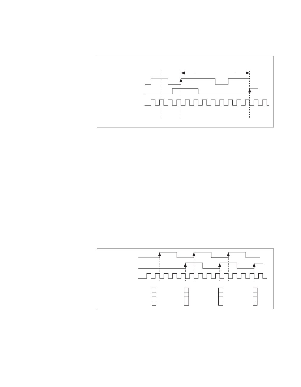
Chapter 9 Counters
Figure 9-20 shows an example of a single two-signal edge-separation
measurement.
Counter
AUX
GATE
SOURCE
Counter Value
HW Save Register
Armed
0000123456788 8
Measured Interval
8
Figure 9-20. Single Two-Signal Edge-Separation Measurement
Buffered Two-Signal Edge-Separation Measurement
Buffered and single two-signal edge-separation measurements are similar,
but buffered measurement measures multiple intervals.
The counter counts the number of rising (or falling) edges on the Source
input occurring between an active edge of the Gate signal and an active
edge of the Aux signal. The counter then stores the count in a hardware save
register. On the next active edge of the Gate signal, the counter begins
another measurement. A USB Signal Stream transfers the stored values to
host memory.
Figure 9-21 shows an example of a buffered two-signal edge-separation
measurement.
AUX
GATE
SOURCE
Counter Value
Buffer
123 123 123
3333
3
3
Figure 9-21. Buffered Two-Signal Edge-Separation Measurement
For information about connecting counter signals, refer to the Default
Counter/Timer Pinouts section.
© National Instruments Corporation 9-19 NI USB-621x User Manual
Page 100

Chapter 9 Counters
Counter Output Applications
Simple Pulse Generation
Single Pulse Generation
The counter can output a single pulse. The pulse appears on the Counter n
Internal Output signal of the counter.
You can specify a delay from when the counter is armed to the beginning
of the pulse. The delay is measured in terms of a number of active edges of
the Source input.
You can specify a pulse width. The pulse width is also measured in terms
of a number of active edges of the Source input. You also can specify the
active edge of the Source input (rising or falling).
Figure 9-22 shows a generation of a pulse with a pulse delay of four and a
pulse width of three (using the rising edge of Source).
Counter Armed
SOURCE
OUT
Figure 9-22. Single Pulse Generation
Single Pulse Generation with Start Trigger
The counter can output a single pulse in response to one pulse on a
hardware Start Trigger signal. The pulse appears on the Counter n Internal
Output signal of the counter.
You can route the Start Trigger signal to the Gate input of the counter. You
can specify a delay from the Start Trigger to the beginning of the pulse. You
also can specify the pulse width. The delay and pulse width are measured
in terms of a number of active edges of the Source input.
After the Start Trigger signal pulses once, the counter ignores the Gate
input.
NI USB-621x User Manual 9-20 ni.com
 Loading...