

Page 1

PXI
NI PXI-4224 User Manual
NI PXI-4224 User Manual
August 2008
373752G-01
Page 2

Support
Worldwide Technical Support and Product Information
ni.com
National Instruments Corporate Headquarters
11500 North Mopac Expressway Austin, Texas 78759-3504 USA Tel: 512 683 0100
Worldwide Offices
Australia 1800 300 800, Austria 43 662 457990-0, Belgium 32 (0) 2 757 0020, Brazil 55 11 3262 3599,
Canada 800 433 3488, China 86 21 5050 9800, Czech Republic 420 224 235 774, Denmark 45 45 76 26 00,
Finland 358 (0) 9 725 72511, France 01 57 66 24 24, Germany 49 89 7413130, India 91 80 41190000,
Israel 972 3 6393737, Italy 39 02 41309277, Japan 0120-527196, Korea 82 02 3451 3400,
Lebanon 961 (0) 1 33 28 28, Malaysia 1800 887710, Mexico 01 800 010 0793, Netherlands 31 (0) 348 433 466,
New Zealand 0800 553 322, Norway 47 (0) 66 90 76 60, Poland 48 22 3390150, Portugal 351 210 311 210,
Russia 7 495 783 6851, Singapore 1800 226 5886, Slovenia 386 3 425 42 00, South Africa 27 0 11 805 8197,
Spain 34 91 640 0085, Sweden 46 (0) 8 587 895 00, Switzerland 41 56 2005151, Taiwan 886 02 2377 2222,
Thailand 662 278 6777, Turkey 90 212 279 3031, United Kingdom 44 (0) 1635 523545
For further support information, refer to the Signal Conditioning Technical Support Information document.
To comment on National Instruments documentation, refer to the National Instruments Web site at
ni.com/info and enter the info code feedback.
© 2004–2008 National Instruments Corporation. All rights reserved.
Page 3

Important Information
Warranty
The NI PXI-4224 is warranted against defects in materials and workmanship for a period of one year from the date of shipment, as evidenced
by receipts or other documentation. National Instruments will, at its option, repair or replace equipment that proves to be defective during the
warranty period. This warranty includes parts and labor.
The media on which you receive National Instruments software are warranted not to fail to execute programming instructions, due to defects in
materials and workmanship, for a period of 90 days from date of shipment, as evidenced by receipts or other documentation. National Instruments
will, at its option, repair or replace software media that do not execute programming instruc tions if National Instruments receives notice of such defects
during the warranty period. National Instruments does not warrant that the operation of the software shall be uninterrupted or error free.
A Return Material Authorization (RMA) number must be obtained from the factory and clearly marked on the outside of the package before any
equipment will be accepted for warranty work. National Instruments will pay the shipping costs of returning to the owner parts which are covered by
warranty.
National Instruments believes that the information in this document is accurate. The document has been carefully reviewed for technical accuracy. In
the event that technical or typographical errors exist, National Instruments reserves the right to make changes to subsequent editions of this document
without prior notice to holders of this edition. The reader should consult National Instruments if errors are suspected. In no event shall National
Instruments be liable for any damages arising out of or related to this document or the information contained in it.
E
XCEPT AS SPECIFIED HEREIN, NATIONAL INSTRUMENTS MAKES NO WARRANTIES, EXPRESS OR IMPLIED, AND SPECIFICALLY DISCLAIMS ANY WARRANTY OF
MERCHANTABILITY OR FITNESS FOR A PARTICULAR PURPOSE. CUSTOMER’S RIGHT TO RECOVER DAMAGES CAUSED BY FAULT OR NEGLIGENCE ON THE PART OF NATIONAL
I
NSTRUMENTS SHALL BE LIMITED TO THE AMOUNT THERETOFORE PAID BY THE CUSTOMER. NATIONAL INSTRUMENTS WILL NOT BE LIABLE FOR DAMAGES RESULTING
FROM LOSS OF DATA, PROFITS, USE OF PRODUCTS, OR INCIDENTAL OR CONSEQUENTIAL DAMAGES, EVEN IF ADVISED OF THE POSSIBILITY THEREOF. This limitation of
the liability of National Instruments will apply regardless of the form of action, whether in contract or tort, including negligence. Any action against
National Instruments must be brought within one year after the cause of action accrues. National Instruments shall not be liable for any delay in
performance due to causes beyond its reasonable control. The warranty provided herein does not cover damages, defects, malfunctions, or service
failures caused by owner’s failure to follow the National Instruments installation, operation, or maintenance instructions; owner’s modification of the
product; owner’s abuse, misuse, or negligent acts; and power failure or surges, fire, flood, accident, actions of third parties, or other events outside
reasonable control.
Copyright
Under the copyright laws, this publication may not be reproduced or transmitted in any form, electronic or mechanical, including photocopying,
recording, storing in an information retrieval system, or translating, in whole or in part, without the prior written consent of National
Instruments Corporation.
National Instruments respects the intellectual property of others, and we ask our users to do the same. NI software is protected by copyright and other
intellectual property laws. Where NI software may be used to reproduce software or other materials belonging to others, you may use NI software only
to reproduce materials that you may reproduce in accordance with the terms of any applicable license or other legal restriction.
Trademarks
National Instruments, NI, ni.com, and LabVIEW are trademarks of National Instruments Corporation. Refer to the Terms of Use section
on
ni.com/legal for more information about National Instruments trademarks.
Other product and company names mentioned herein are trademarks or trade names of their respective companies.
Patents
For patents covering National Instruments products/technology, refer to the appropriate location: Help»Patents in your software,
the
patents.txt file on your media, or the National Instruments Patent Notice at ni.com/patents.
WARNING REGARDING USE OF NATIONAL INSTRUMENTS PRODUCTS
(1) NATIONAL INSTRUMENTS PRODUCTS ARE NOT DESIGNED WITH COMPONENTS AND TESTING FOR A LEVEL OF
RELIABILITY SUITABLE FOR USE IN OR IN CONNECTION WITH SURGICAL IMPLANTS OR AS CRITICAL COMPONENTS IN
ANY LIFE SUPPORT SYSTEMS WHOSE FAILURE TO PERFORM CAN REASONABLY BE EXPECTED TO CAUSE SIGNIFICANT
INJURY TO A HUMAN.
(2) IN ANY APPLICATION, INCLUDING THE ABOVE, RELIABILITY OF OPERATION OF THE SOFTWARE PRODUCTS CAN BE
IMPAIRED BY ADVERSE FACTORS, INCLUDING BUT NOT LIMITED TO FLUCTUATIONS IN ELECTRICAL POWER SUPPLY,
COMPUTER HARDWARE MALFUNCTIONS, COMPUTER OPERATING SYSTEM SOFTWARE FITNESS, FITNESS OF COMPILERS
AND DEVELOPMENT SOFTWARE USED TO DEVELOP AN APPLICATION, INSTALLATION ERRORS, SOFTWARE AND HARDWARE
COMPATIBILITY PROBLEMS, MALFUNCTIONS OR FAILURES OF ELECTRONIC MONITORING OR CONTROL DEVICES,
TRANSIENT FAILURES OF ELECTRONIC SYSTEMS (HARDWARE AND/OR SOFTWARE), UNANTICIPATED USES OR MISUSES, OR
ERRORS ON THE PART OF THE USER OR APPLICATIONS DESIGNER (ADVERSE FACTORS SUCH AS THESE ARE HEREAFTER
COLLECTIVELY TERMED “SYSTEM FAILURES”). ANY APPLICATION WHERE A SYSTEM FAILURE WOULD CREATE A RISK OF
HARM TO PROPERTY OR PERSONS (INCLUDING THE RISK OF BODILY INJURY AND DEATH) SHOULD NOT BE RELIANT SOLELY
UPON ONE FORM OF ELECTRONIC SYSTEM DUE TO THE RISK OF SYSTEM FAILURE. TO AVOID DAMAGE, INJURY, OR DEATH,
THE USER OR APPLICATION DESIGNER MUST TAKE REASONABLY PRUDENT STEPS TO PROTECT AGAINST SYSTEM FAILURES,
INCLUDING BUT NOT LIMITED TO BACK-UP OR SHUT DOWN MECHANISMS. BECAUSE EACH END-USER SYSTEM IS
CUSTOMIZED AND DIFFERS FROM NATIONAL INSTRUMENTS' TESTING PLATFORMS AND BECAUSE A USER OR APPLICATION
DESIGNER MAY USE NATIONAL INSTRUMENTS PRODUCTS IN COMBINATION WITH OTHER PRODUCTS IN A MANNER NOT
EVALUATED OR CONTEMPLATED BY NATIONAL INSTRUMENTS, THE USER OR APPLICATION DESIGNER IS ULTIMATELY
RESPONSIBLE FOR VERIFYING AND VALIDATING THE SUITABILITY OF NATIONAL INSTRUMENTS PRODUCTS WHENEVER
NATIONAL INSTRUMENTS PRODUCTS ARE INCORPORATED IN A SYSTEM OR APPLICATION, INCLUDING, WITHOUT
LIMITATION, THE APPROPRIATE DESIGN, PROCESS AND SAFETY LEVEL OF SUCH SYSTEM OR APPLICATION.
Page 4
Conventions
The following conventions are used in this manual:
<> Angle brackets that contain numbers separated by an ellipsis represent a
range of values associated with a bit or signal name—for example,
AO <3. .0>.
» The » symbol leads you through nested menu items and dialog box options
to a final action. The sequence File»Page Setup»Options directs you to
pull down the File menu, select the Page Setup item, and select Options
from the last dialog box.
This icon denotes a note, which alerts you to important information.
This icon denotes a caution, which advises you of precautions to take to
avoid injury, data loss, or a system crash. When this symbol is marked on
the product, refer to the Read Me First: Safety and Radio-Frequency
Interference document, shipped with the product, for precautions to take.
When symbol is marked on a product it denotes a warning advising you to
take precautions to avoid electrical shock.
When symbol is marked on a product it denotes a component that may be
hot. Touching this component may result in bodily injury.
bold Bold text denotes items that you must select or click in the software, such
as menu items and dialog box options. Bold text also denotes parameter
names.
italic Italic text denotes variables, emphasis, a cross-reference, hardware labels,
or an introduction to a key concept. Italic text also denotes text that is a
placeholder for a word or value that you must supply.
monospace Text in this font denotes text or characters that you should enter from the
keyboard, sections of code, programming examples, and syntax examples.
This font is also used for the proper names of disk drives, paths, directories,
programs, subprograms, subroutines, device names, functions, operations,
variables, filenames and extensions, and code excerpts.
Page 5

Contents
Chapter 1
About the NI PXI-4224
What You Need to Get Started ......................................................................................1-2
National Instruments Documentation ............................................................................1-3
Installing the Application Software, NI-DAQ, and the DAQ Device ...........................1-3
Installing the NI PXI-4224 ............................................................................................1-4
LED Pattern Descriptions ..............................................................................................1-4
Chapter 2
Connecting Signals
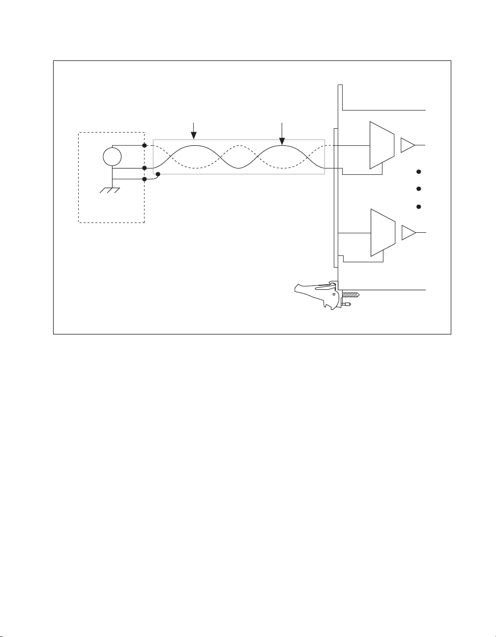
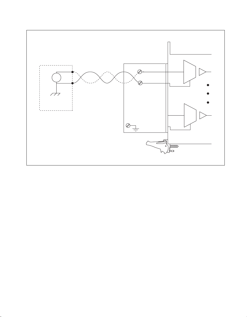
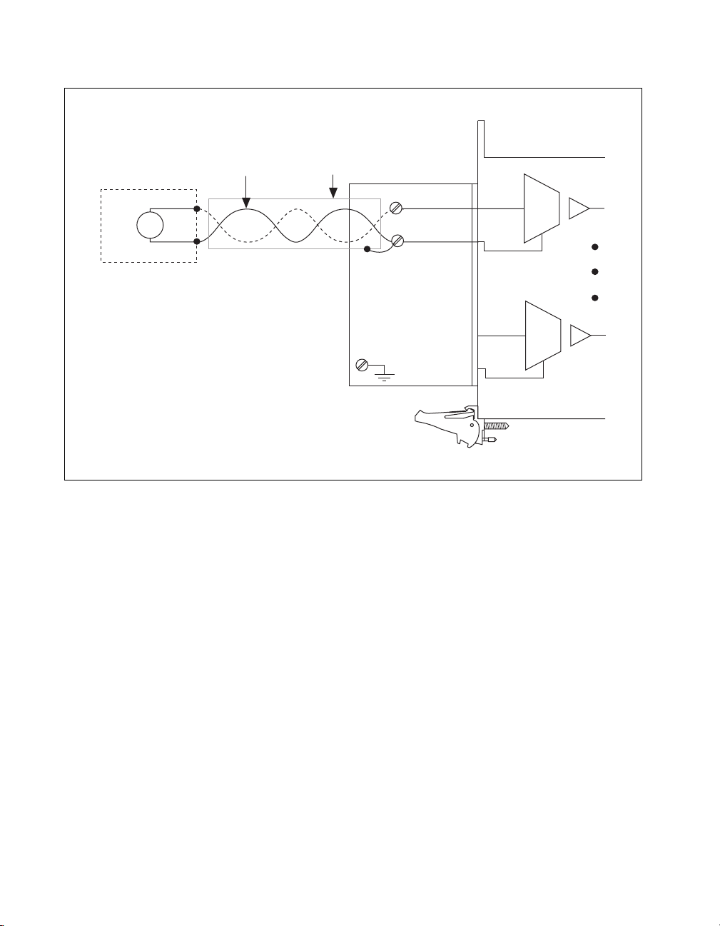
Connecting Signals to the NI PXI-4224 ........................................................................2-1
Front Signal Connector....................................................................................2-1
Analog Input Connections...............................................................................2-3
Floating Signal Source Connection...................................................2-11
Ground-Referenced Signal Connection ............................................2-12
Shielded Ground-Referenced Signal Connection
(Recommended) .............................................................................2-12
Chapter 3
Configuring and Testing
Verifying and Self-Testing the Signals Using Test Panels ............................................3-1
Configuring the NI PXI-4224 in MAX..........................................................................3-2
Creating a Voltage Task or Global Channel Using NI-DAQmx.....................3-2
Verifying and Self-Testing an NI-DAQmx Task or Global Channel.............. 3-3
Chapter 4
Theory of Operation
Theory of Operation.......................................................................................................4-1
Signal Conditioning Functional Overview ......................................................4-3
Measurement Considerations ..........................................................................4-3
Input Impedance................................................................................4-3
Common-Mode Rejection Ratio .......................................................4-4
Effective CMR ..................................................................................4-5
Timing and Control Functional Overview ......................................................4-5
Programmable Function Inputs .......................................................................4-6
Device and PXI Clocks ...................................................................................4-7
© National Instruments Corporation v NI PXI-4224 User Manual
Page 6

Contents
Chapter 5
Using the NI PXI-4224
Developing Your Application ....................................................................................... 5-1
Typical Program Flow Chart........................................................................... 5-1
Overview of Typical Flow Chart .................................................................... 5-3
Creating a Task Using DAQ Assistant or Programmatically ........... 5-3
Adjusting Timing and Triggering..................................................... 5-3
Configuring Channel Properties ....................................................... 5-4
Acquiring, Analyzing, and Presenting.............................................. 5-5
Completing the Application.............................................................. 5-5
Developing an Application Using LabVIEW ................................................. 5-5
Using a DAQmx Channel Property Node in LabVIEW................... 5-7
Synchronization and Triggering...................................................................... 5-8
Synchronizing the NI PXI-4224 ..................................................................... 5-8
Synchronizing the NI PXI-4224 Using LabVIEW ........................... 5-10
Other Application Documentation and Material ........................................................... 5-11
Calibrating the NI PXI-4224 ......................................................................................... 5-12
Loading Calibration Constants........................................................................ 5-12
Self-Calibration............................................................................................... 5-12
External Calibration ........................................................................................ 5-13
Appendix A
Specifications
Appendix B
Timing Signal Information
Appendix C
Removing the NI PXI-4224
Appendix D
Common Questions
Glossary
Index
NI PXI-4224 User Manual vi ni.com
Page 7

Figures
Contents
Figure 2-1. NI PXI-4224 Front Label ......................................................................2-3
Figure 2-2. Unshielded Floating Signal Source Connection
Using a D-SUB Connector ....................................................................2-4
Figure 2-3. Unshielded Grounded Signal Source Connection
Using a D-SUB Connector ....................................................................2-5
Figure 2-4. Shielded Floating Signal Source Connection
Using a D-SUB Connector ....................................................................2-6
Figure 2-5. Shielded Grounded Signal Source Connection
Using a D-SUB Connector ....................................................................2-7
Figure 2-6. Unshielded Floating Signal Source Connection
Using a Terminal Block ........................................................................2-8
Figure 2-7. Unshielded Grounded Signal Source Connection
Using a Terminal Block ........................................................................2-9
Figure 2-8. Shielded Floating Signal Source Connection
Using a Terminal Block ........................................................................2-10
Figure 2-9. Shielded Grounded Signal Source Connection
Using a Terminal Block ........................................................................2-11
Figure 4-1. Block Diagram of NI PXI-4224 ............................................................4-2
Figure 4-2. Effect of Input Impedance on Signal Measurements ............................4-4
Figure 4-3. AI CONV CLK Signal Routing ............................................................4-6
Figure 4-4. NI PXI-4224 PXI Trigger Bus Signal Connection................................4-8
Figure 5-1. Typical Program Flowchart...................................................................5-2
Figure 5-2. General Synchronizing Flowchart.........................................................5-9
Figure A-1. PXI-4224 Dimensions ...........................................................................A-4
Figure B-1. Typical Posttriggered Sequence ............................................................B-2
Figure B-2. Typical Pretriggered Sequence..............................................................B-2
Figure B-3. AI START TRIG Input Signal Timing .................................................B-3
Figure B-4. AI START TRIG Output Signal Timing...............................................B-3
Figure B-5. AI REF TRIG Input Signal Timing.......................................................B-4
Figure B-6. AI REF TRIG Output Signal Timing ....................................................B-5
Figure B-7. AI SAMP CLK Input Signal Timing ....................................................B-6
Figure B-8. AI SAMP CLK Output Signal Timing..................................................B-6
Figure B-9. AI CONV CLK Input Signal Timing ....................................................B-7
Figure B-10. AI CONV CLK Output Signal Timing .................................................B-8
Figure B-11. AI SAMPLE CLK TIMEBASE Signal Timing....................................B-9
Figure B-12. AI HOLD COMPLETE Signal Timing.................................................B-10
Figure C-1. Injector/Ejector Handle Position Before Device Removal....................C-2
© National Instruments Corporation vii NI PXI-4224 User Manual
Page 8

Contents
Tables
Table 2-1. NI PXI-4224 25-Pin D-SUB Terminal Pin Assignments ..................... 2-2
Table 4-1. Signal Conditioning Functional Blocks ................................................ 4-3
Table 4-2. PXI Trigger Bus Timing Signals .......................................................... 4-9
Table 5-1. NI-DAQmx Properties .......................................................................... 5-4
Table 5-2. Programming a Task in LabVIEW ....................................................... 5-6
Table 5-3. Synchronizing the NI PXI-4224 Using LabVIEW ............................... 5-10
Table A-1. Maximum Sampling Rates.................................................................... A-1
NI PXI-4224 User Manual viii ni.com
Page 9

About the NI PXI-4224
This chapter provides an introduction to the NI PXI-4224 device and its
installation.
The NI PXI-4224 is part of the NI PXI-4200 series of data acquisition
(DAQ) devices with integrated signal conditioning. The PXI-4200 series
reduces measurement setup and configuration complexity by integrating
signal conditioning and DAQ on the same product.
The NI PXI-4224 is an 8-channel isolated analog input device with a ±10 V
input range. It allows isolated analog measurements directly on the PXI
platform.
The NI PXI-4224 has the following characteristics:
• Each channel has a gain of either 1 or 10.
• An isolation rating of 42.4 V
• The front connector is a 25-pin D-SUB connector, with 16 pins for
analog input.
or 60 VDC, Category I.
peak
1
Signal connections are made through a TB-2725 terminal block that
provides connections for all eight analog input channels. You can
optionally connect a standard 25-pin D-SUB cable to the device and cable
it as needed for your application.
Note Go to ni.com/products to determine if newly developed terminal blocks are
available.
You can configure most settings on a per-channel basis through software.
The NI PXI-4224 is configured using Measurement & Automation
Explorer (MAX) or through function calls to NI-DAQmx.
Note The NI PXI-4224 is supported in NI-DAQmx only.
© National Instruments Corporation 1-1 NI PXI-4224 User Manual
Page 10

Chapter 1 About the NI PXI-4224
What You Need to Get Started
To set up and use the NI PXI-4224, you need the following:
❑ Hardware
–NIPXI-4224
– One of the following:
• TB-2725 terminal block
• 25-pin D-SUB female connector
– PXI or PXI/SCXI combination chassis
❑ Software
– NI-DAQ 7.3.1 or later
– One of the following:
•LabVIEW
• Measurement Studio
• LabWindows
❑ Documentation
– NI PXI-4224 User Manual
– Read Me First: Safety and Radio-Frequency Interference
– DAQ Getting Started Guide
– PXI or PXI/SCXI combination chassis user manual
– Documentation for your software
™
/CVI
™
❑ Tools
– 1/8 in. flathead screwdriver
You can download NI documents from
NI PXI-4224 User Manual 1-2 ni.com
ni.com/manuals.
Page 11

National Instruments Documentation
The NI PXI-4224 User Manual is one piece of the documentation set for
your DAQ system. You could have any of several types of manuals
depending on the hardware and software in your system. Use the manuals
you have as follows:
• DAQ Getting Started Guide—This document describes how to install
NI-DAQ devices and NI-DAQ. Install NI-DAQmx before you install
the SCXI module.
• SCXI Quick Start Guide—This document describes how to set up an
SCXI chassis, install SCXI modules and terminal blocks, and
configure the SCXI system in MAX.
• PXI or PXI/SCXI combination chassis manual—Read this manual for
maintenance information about the chassis and for installation
instructions.
• Accessory installation guides or manuals—If you are using accessory
products, read the terminal block installation guides. They explain how
to physically connect the relevant pieces of the system.
• Software documentation—You may have both application software
and NI-DAQmx software documentation. NI application software
includes LabVIEW, Measurement Studio, and LabWindows/CVI.
After you set up the hardware system, use either your application
software documentation or the NI-DAQmx documentation to help you
write your application. If you have a large, complicated system, it is
worthwhile to look through the software documentation before you
configure the hardware.
Chapter 1 About the NI PXI-4224
Installing the Application Software, NI-DAQ, and the DAQ Device
Refer to the DAQ Getting Started Guide, packaged with the NI-DAQ
software, for instructions for installing your application software, NI-DAQ
driver software, and the DAQ device to which you will connect the
NI PXI-4224.
NI-DAQ 7.3.1 or later is required to configure and program the
NI PXI-4224 device. If you do not have NI-DAQ 7.3.1 or later, you can
either contact an NI sales representative to request it on a CD or download
ni.com.
it from
© National Instruments Corporation 1-3 NI PXI-4224 User Manual
Page 12

Chapter 1 About the NI PXI-4224
Installing the NI PXI-4224
Note Refer to the Read Me First: Radio-Frequency Interference document before
removing equipment covers or connecting or disconnecting any signal wires.
Refer to the DAQ Getting Started Guide to unpack, install, and configure
the NI PXI-4224 in a PXI chassis, and then to the SCXI Quick Start Guide
if you are using a PXI/SCXI combination chassis.
LED Pattern Descriptions
The following LEDs on the NI PXI-4224 front panel confirm the system is
functioning properly:
• The ACCESS LED is normally green and blinks yellow for a minimum
of 100 ms during the NI PXI-4224 configuration.
• The ACTIVE LED is normally green and blinks yellow for a minimum
of 100 ms during data acquisition.
NI PXI-4224 User Manual 1-4 ni.com
Page 13

Connecting Signals
This chapter provides details about the front signal connector of the
NI PXI-4224 and how to connect signals to the NI PXI-4224.
Connecting Signals to the NI PXI-4224
After you have verified that the NI PXI-4224 is installed correctly and
self-tested the device, refer to the following sections to connect signals to
the device.
Caution Refer to the Read Me First: Safety and Radio-Frequency Interference document
before removing equipment covers, or connecting or disconnecting any signal wires.
Front Signal Connector
The NI PXI-4224 connection interface consists of a 25-pin D-SUB
connector and one SMB connector. You can program SMB connector
as a PFI 0 line or for external calibration. Table 2-1 shows the signal
assignments of the D-SUB connector for the NI PXI-4224. Figure 2-1
shows the front label, with each set of screw terminals labeled according
to the corresponding differential input signal for the NI PXI-4224.
2
To connect a signal to the NI PXI-4224, use a TB-2725 terminal block
designed specifically for the NI-PXI-4224, or use a 25-pin D-SUB to build
a connector to suit your application. Refer to the TB-2725 Terminal Block
Installation Guide if you are using the TB-2725 terminal block. Use
Table 2-1 to make the signal connections if you are constructing a
connector using a 25-pin D-SUB connector.
Connect a timing or triggering signal to the PFI 0/CAL SMB connector
using a cable with an SMB signal connector.
© National Instruments Corporation 2-1 NI PXI-4224 User Manual
Page 14

Chapter 2 Connecting Signals
Caution The PFI 0/CAL SMB connector is for low-voltage timing and calibration signals
only. Voltages greater than ±15 V can damage the device.
If you are building a 25-pin D-SUB connector for your application, make sure you use a
connector and wires that are safety rated for the voltage and category of the signals in your
application.
Table 2-1. NI PXI-4224 25-Pin D-SUB Terminal Pin Assignments
Front Connector
Diagram
14 15 16 17 18 19 20 21 22 23 24 25
12345678910111213
Pin Number Signal Names Pin Number Signal Names
14 AI 0 – 1 AI 0 +
15 AI 1 – 2 AI 1 +
16 AI 2 – 3 AI 2 +
17 AI 3 – 4 AI 3 +
18 AI 4 – 5 AI 4 +
19 AI 5 – 6 AI 5 +
*
NC—No Connection
20 AI 6 – 7 AI 6 +
21 AI 7 – 8 AI 7 +
22 No Pin 9 No Pin
23 NC
*
10 D GND
24 SPI CLK 11 MISO
25 SELECT 12 MOSI
N/A N/A 13 +5 V
NI PXI-4224 User Manual 2-2 ni.com
Page 15
Chapter 2 Connecting Signals
NI PXI-4224
8 Chan Isolation Amp
ACCESS ACTIVE
2
PFI 0/
CAL
12345678910111213
14 15 16 17 18 19 20 21 22 23 24 25
1
3
1 ACCESS and ACTIVE LEDs
2 SMB PFI 0/CAL Connector
3 25-Pin D-SUB or TB-2725 Terminal
Block Connector
Figure 2-1. NI PXI-4224 Front Label
Analog Input Connections
The following sections provide a definition of the signal source
characteristics, descriptions of various ways to connect signals to the
NI PXI-4224, and electrical diagrams showing the signal source and
connections. Whenever possible, use shielded twisted-pair field wiring
and grounding to reduce the effects of unwanted noise sources.
© National Instruments Corporation 2-3 NI PXI-4224 User Manual
Page 16
Chapter 2 Connecting Signals
Caution If you are building a 25-pin D-SUB connector for your application, make sure
you use a connector and signal wires that are safety rated for the voltage and category of
the signals in your application.
In the electrical diagrams, two different ground symbols are used. These
symbols indicate that you cannot assume that the indicated grounds are at
the same potential. Refer to Appendix A, Specifications, for maximum
working voltage specifications.
You can make signal connections to the NI PXI-4224 through either an
NI terminal block, such as the TB-2725, or you can build a connector using
a 25-pin D-SUB.
Figures 2-2 through 2-5 illustrate connecting signals using a D-SUB
connector.
Signal Source
+
V
SIG
–
Tw isted-Pair
Wiring
AI 0 +
AI 0 –
AI 7 +
AI 7 –
CH 0
CH 7
Figure 2-2. Unshielded Floating Signal Source Connection Using a D-SUB Connector
NI PXI-4224 User Manual 2-4 ni.com
Page 17

Chapter 2 Connecting Signals
Signal Source
+
V
SIG
–
V
Ground
SIG
Reference
Tw isted-Pair
Wiring
AI 0 +
CH 0
AI 0 –
CH 7
AI 7 +
AI 7 –
Figure 2-3. Unshielded Grounded Signal Source Connection Using a D-SUB Connector
© National Instruments Corporation 2-5 NI PXI-4224 User Manual
Page 18
Chapter 2 Connecting Signals
Signal Source
+
V
SIG
–
Shielding
Wiring
CH 0
AI 0 +
AI 0 –
CH 7
AI 7 +
AI 7 –
Figure 2-4. Shielded Floating Signal Source Connection Using a D-SUB Connector
Tw isted-Pair
NI PXI-4224 User Manual 2-6 ni.com
Page 19
Chapter 2 Connecting Signals
Signal Source
+
V
SIG
–
V
Ground
SIG
Reference
Shielding
Wiring
CH 0
AI 0 +
AI 0 –
CH 7
AI 7 +
AI 7 –
Figure 2-5. Shielded Grounded Signal Source Connection Using a D-SUB Connector
Tw isted-Pair
© National Instruments Corporation 2-7 NI PXI-4224 User Manual
Page 20
Chapter 2 Connecting Signals
Figures 2-6 through 2-9 illustrate connecting signals using a terminal
block.
Signal Source
+
V
SIG
–
Tw isted-Pair
Wiring
Terminal Block
AI 0 +
AI 0 –
AI 7 +
AI 7 –
CH 0
CH 7
Figure 2-6. Unshielded Floating Signal Source Connection Using a Terminal Block
NI PXI-4224 User Manual 2-8 ni.com
Page 21
Chapter 2 Connecting Signals
Signal Source
+
V
SIG
–
V
Ground
SIG
Reference
Tw isted-Pair
Wiring
Terminal Block
AI 0 +
CH 0
AI 0 –
CH 7
AI 7 +
AI 7 –
Figure 2-7. Unshielded Grounded Signal Source Connection Using a Terminal Block
© National Instruments Corporation 2-9 NI PXI-4224 User Manual
Page 22
Chapter 2 Connecting Signals
Signal Source
+
V
SIG
–
Tw isted-Pair
Wiring
Shielding
Terminal Block
CH 0
AI 0 +
AI 0 –
CH 7
AI 7 +
AI 7 –
Figure 2-8. Shielded Floating Signal Source Connection Using a Terminal Block
NI PXI-4224 User Manual 2-10 ni.com
Page 23
Chapter 2 Connecting Signals
Signal Source
+
V
SIG
–
V
Ground
SIG
Reference
Tw isted-Pair
Wiring
Shielding
Terminal Block
CH 0
AI 0 +
AI 0 –
CH 7
AI 7 +
AI 7 –
Figure 2-9. Shielded Grounded Signal Source Connection Using a Terminal Block
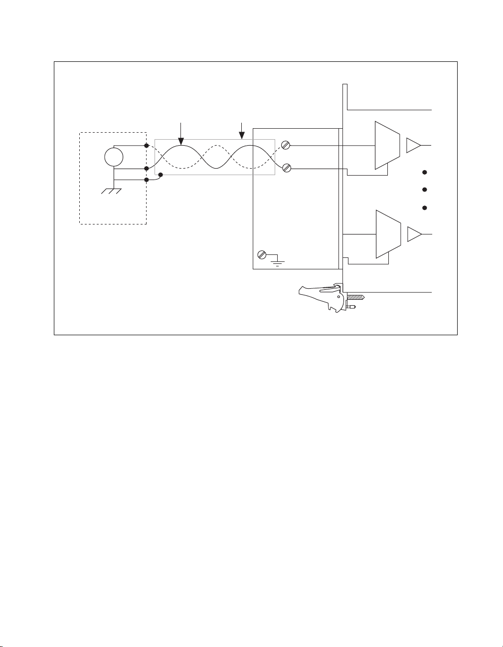
Floating Signal Source Connection
Figures 2-2, 2-4, 2-6, and 2-8 illustrate floating signal source connections.
In this configuration, the signal source being measured is a floating signal
source, such as a battery. A floating signal source is not connected in
any way to the building ground system.
To connect a floating signal source connection to the NI PXI-4224, the
signal (V
signal reference (V
© National Instruments Corporation 2-11 NI PXI-4224 User Manual
+) is connected to the NI PXI-4224 channel (AI X +). The
SIG
–) is connected to the channel reference (AI X –).
SIG
Page 24

Chapter 2 Connecting Signals
Ground-Referenced Signal Connection
Figures 2-3, 2-5, 2-7, and 2-9 illustrate the ground-referenced signal
connection. In this configuration, the voltage source being measured is
referenced to its own ground reference that is connected through a
conductive path to the instrument ground reference. For example, the path
can be through a common earth ground or through the power line ground.
To connect a ground-reference signal source to the NI PXI-4224, the signal
+) is connected to the NI PXI-4224 channel (AI X +). The signal
(V
SIG
reference (V
–) is connected to the channel reference (AI X –).
SIG
Shielded Ground-Referenced Signal Connection (Recommended)
Figures 2-5 and 2-9 illustrate shielded ground-referenced signal
connections. The connection to this signal source is identical to the
ground-referenced signal connection with the addition of shielding
around the field wiring. The shielding is grounded at the signal source
ground (V
Ground Reference). Connect the signal (V
SIG
NI PXI-4224 channel (AI X +). Connect the signal reference (V
channel reference (AI X –).
+) to the
SIG
–) to the
SIG
This shielding scheme is effective at reducing capacitive or electrically
coupled noise. The same concerns regarding the difference in ground
potentials, discussed in the Ground-Referenced Signal Connection section,
also apply to this configuration.
For more information about the function of the NI PXI-4224 and other
measurement considerations, refer to Chapter 4, Theory of Operation.
NI PXI-4224 User Manual 2-12 ni.com
Page 25

3
Configuring and Testing
This chapter provides details about configuring and testing the
NI PXI-4224 in MAX, including how to use device test panels and create
and configure NI-DAQmx Tasks and NI-DAQmx Global Channels.
Verifying and Self-Testing the Signals Using Test Panels
After you have successfully installed the NI PXI-4224, verified the
installation, and connected the signals, use the NI PXI-4224 device test
panels to verify the device is measuring signals properly.
The test panels allow you to measure the signal connected to the
NI PXI-4224 directly as well as configure some of the properties of your
measurement. To open the NI PXI-4224 device test panels when in MAX,
complete the following steps:
1. Expand Devices and Interfaces to display the list of devices and
interfaces.
2. Expand NI-DAQmx Devices to display the list of NI-DAQmx devices.
3. Click PXI-4224.
4. Click the Test Panels button in the device toolbar.
5. Configure the settings on the screen, and click Start to take a
measurement.
To measure scaled voltages, further configure channel properties, and
configure timing settings, use an NI-DAQmx Task or NI-DAQmx Global
Channel.
© National Instruments Corporation 3-1 NI PXI-4224 User Manual
Page 26

Chapter 3 Configuring and Testing
Configuring the NI PXI-4224 in MAX
This section describes how to create NI-DAQmx Tasks and NI-DAQmx
Global Channels in MAX that allow you to take measurements with the
NI PXI-4224.
Creating a Voltage Task or Global Channel Using NI-DAQmx
An NI-DAQmx Global Channel gives a physical channel a name and
provides scaling. An NI-DAQmx Task is a collection of channels with
timing and triggering configured. To create a new NI-DAQmx Task or
NI-DAQmx Global Channel, complete the following steps:
1. Double-click the Measurement & Automation Explorer icon on the
desktop.
2. Right-click Data Neighborhood and select Create New.
3. Select NI-DAQmx Task or NI-DAQmx Global Channel and
click Next.
4. Select Analog Input and select Voltage.
5. If you are creating a channel, you can select only one channel. If you
are creating a task, select the channels to add to the task. You can select
a range of channels by holding down the <Shift> key while selecting
the channels. You can select multiple individual channels by holding
down the <Ctrl> key while selecting channels. Click Next.
6. Enter the name of the task or channel, and click Finish.
7. Select the channel(s) you want to configure for input voltage range.
While making the selections you can select blocks of channels by
pressing the <Shift> key or individual channels by pressing the
<Ctrl> key.
8. Under the Settings tab, set the input range by entering the Min and
Max values.
9. Click the Device tab and select the Autozero mode.
10. Repeat steps 7 through 9 until you have configured all the channels.
Note For more information about how to further configure the NI PXI-4224, or how to use
LabVIEW to configure the device and take measurements, refer to Chapter 4, Theory of
Operation.
NI PXI-4224 User Manual 3-2 ni.com
Page 27

Chapter 3 Configuring and Testing
Verifying and Self-Testing an NI-DAQmx Task or Global Channel
After you have created an analog input voltage NI-DAQmx Task or
NI-DAQmx Global Channel, verify the NI-DAQmx Task or NI-DAQmx
Global Channel signal and functionality using the Test button in the
toolbar:
1. If you created an NI-DAQmx Task, set the timing and triggering
settings you wish to use in the test in the Task Timing and Task
Triggering tabs.
2. Click the Test button to open the test panel and take a measurement.
You have now verified the NI PXI-4224 configuration and signal
connection.
© National Instruments Corporation 3-3 NI PXI-4224 User Manual
Page 28

Theory of Operation
This chapter describes the theory of operation, measurement
considerations, and timing information.
Theory of Operation
Figure 4-1 illustrates the key functional components of the NI PXI-4224,
including the DAQ and integrated signal conditioning circuitry.
4
© National Instruments Corporation 4-1 NI PXI-4224 User Manual
Page 29

Chapter 4 Theory of Operation
ADC
FIFO
A/D
Converter
NI-PGA
Calibration DACs
Mode
Analog
Analog
Multiplexor
Input
MUX
Ref
Voltage
PXI Connector
Control
Address/Data
PCI
Bus
MITE
MINI-
Interface
DMA
and
DIO
Play
Plug
82C55
Interface
Control
Configuration
Memory
EEPROM
SMB
Temp Sensor
Cal
MUX
References
Signal Cond
Bus
Generic
Interface
Data
EEPROM
IRQ
AI Control
DMA
EEPROM
Analog
DMA/
Input
Interrupt
Control
Control
Request
DAQ-STC
Bus
DAQ-APE
Bus
Interface
Interface
Bus
RTSI Bus
RTSI
Interface
Interface
DAQ-STC
Analog Input
Timing/Control
I/O
Opto
Isolation
Digital
Post
Filter
ISO
Amp
PGA
Input
Protection
AI7
Opto
Isolation
Post
Filter
ISO
Amp
PGA
Input
Protection
AI0
Opto
Isolation
Post
Filter
ISO
Amp
PGA
Input
Protection
AI1
Opto
Isolation
Post
Filter
ISO
Amp
PGA
Input
Protection
AI2
Opto
Isolation
Post
Filter
ISO
Amp
PGA
Input
Protection
AI3
Opto
Isolation
Post
Filter
ISO
Amp
PGA
Input
Protection
AI4
Opto
Isolation
Post
Filter
ISO
Amp
PGA
Input
Protection
AI5
Opto
Isolation
Trigger
Post
Filter
ISO
Amp
PGA
Input
Protection
AI6
Interface
Figure 4-1. Block Diagram of NI PXI-4224
NI PXI-4224 User Manual 4-2 ni.com
Page 30

Chapter 4 Theory of Operation
Signal Conditioning Functional Overview
The NI PXI-4224 is part of the PXI-4200 series of DAQ devices with
integrated signal conditioning designed to provide application-specific
signal conditioning, DAQ, and integrated field wiring connectivity on the
same product. The NI PXI-4224 signal conditioning circuitry is designed
to provide attenuation, amplification, and filtering capabilities as described
in Table 4-1.
Table 4-1. Signal Conditioning Functional Blocks
Signal Conditioning Component Description
Input Protection Each NI PXI-4224 channel has overvoltage protection in the
event that a channel is improperly wired.
PGA Each channel has a programmable gain amplifier. The
available gains on the NI PXI-4224 are 1 and 10, which
covers the input range of ±1 V to ±10 V. The DAQ device can
provide a gain of up to 200 in order to maximize the ADC
resolution for signals below 1 V.
Isolation Amplifier Each channel has an isolation amplifier that creates true
channel-to-channel isolation.
Post Filter A post filter is provided to clean up noise spikes created by
the isolation amplifier.
Measurement Considerations
This section provides more information about the type of signal connection
made to the NI PXI-4224 and important factors that can affect your
measurement.
Input Impedance
Figure 4-2 illustrates the input impedance of an NI PXI-4224 and its effect
on the measurement of a circuit under test. If you know the source
impedance of the circuit under test, you can correct for the attenuation
caused by the NI PXI-4224 in software. Since R
(1 GΩ), it requires a large source impedance, R
change in the measured voltage, V
. In general, a source impedance of
MEAS
less than 200 kΩ does not interfere with the accuracy of the measurement.
For example, a 200 kΩ source impedance results in a 0.02% gain error.
© National Instruments Corporation 4-3 NI PXI-4224 User Manual
is relatively large
IN
, to cause a significant
S
Page 31

Chapter 4 Theory of Operation
Signal Source
SIG
+
–
V
Source
Impedance
R
S
C
100
pF
IN
R
IN
Input
Impedance
+
Measured
Voltage
V
MEAS
–
Figure 4-2. Effect of Input Impedance on Signal Measurements
Although RS does not influence DC measurements, take care when
measuring AC signals since C
attenuates higher frequencies if RS is too
IN
large. For example:
V
SIGRIN
V
MEAS
--------------------=
RSRIN+
1
Bandwidth
----------------------=
2π R
SCIN
Common-Mode Rejection Ratio
The ability of a measurement device to reject voltages that are common to
both input terminals is referred to as the common-mode rejection ratio
(CMRR). The CMMR is usually stated in decibels at a given frequency or
over a given frequency band of interest. Common-mode signals can arise
from a variety of sources and can be induced through conductive or
radiated means. One of the most common sources of common-mode
interference is 50 or 60 Hz powerline noise.
The minimum NI PXI-4224 CMRR is 140 dB, which results in a reduction
of CMV by a factor of 10,000,000.
NI PXI-4224 User Manual 4-4 ni.com
Page 32

Effective CMR
When the frequency of a common-mode signal is known and outside of the
measurement frequency band of interest, you can use an analog or digital
filter, or both, to further reduce the residual error left from the finite CMRR
of the instrument. The combined CMR of the instrument and the filter
attenuation results in an effective CMR. When expressed in decibels, the
effective CMR is equal to the sum of the CMRR and the attenuation due to
the filter at a specified frequency.
Timing and Control Functional Overview
The NI PXI-4224 is based on the NI E Series DAQ device architecture.
This architecture uses the NI data acquisition system timing controller
(DAQ-STC) for time-related functions. The DAQ-STC consists of
two timing groups that control AI and general-purpose counter/timer
functions. These groups include a total of seven 24-bit and three 16-bit
counters and a maximum timing resolution of 50 ns. The DAQ-STC makes
possible applications such as equivalent time sampling, and seamless
changing of the sampling rate.
The NI PXI-4224 uses the PXI trigger bus to easily synchronize several
measurement functions to a common trigger or timing event. The PXI
trigger bus is connected through the rear signal connector to the
PXI chassis backplane. The DAQ-STC provides a flexible interface for
connecting timing signals to other devices or external circuitry. The
NI PXI-4224 uses the PXI trigger bus to interconnect timing signals
between PXI devices, and the programmable function input (PFI) pin on
the front SMB connector to connect the device to external circuitry. These
connections are designed to enable the device to both control and be
controlled by other devices and circuits.
Chapter 4 Theory of Operation
The DAQ-STC has internal timing signals you can control by an external
source. These timing signals also can be controlled by signals internally
generated to the DAQ-STC, and these signals are software configurable.
Figure 4-3 shows an example of the signal routing multiplexer controlling
the AI CONVERT CLOCK signal.
© National Instruments Corporation 4-5 NI PXI-4224 User Manual
Page 33

Chapter 4 Theory of Operation
PXI Trigger<0..5>
Ctr 0 Internal Output
Figure 4-3 shows that AI CONV CLK can be generated from a number of
sources, such as the external signals PFI 0, PXI_Trig<0..5>, and PXI_Star,
and the Ctr 0 Internal Output.
Programmable Function Inputs
PFI 0 is connected to the front SMB connector of the NI PXI-4224.
Software can select PFI 0 as the external source for a given timing signal.
Any timing signal can use the PFI 0 pin as an input, and multiple timing
signals can simultaneously use the same PFI. This flexible routing scheme
reduces the need to change physical connections to the I/O connector for
different applications. Refer to Table 4-2 for information regarding the
available PFI 0 signals.
PXI Star
AI CONV CLK
PFI 0
Figure 4-3. AI CONV CLK Signal Routing
NI PXI-4224 User Manual 4-6 ni.com
Page 34

Device and PXI Clocks
Many functions performed by the NI PXI-4224 require a frequency
timebase to generate the necessary timing signals for controlling
A/D conversions, digital-to-analog converter (DAC) updates, or
general-purpose signals at the I/O connector.
The NI PXI-4224 can use either its internal 20 MHz master timebase or a
timebase received over the PXI trigger bus on the PXI clock line. These
timebases are software configurable. If you configure the device to use the
internal timebase, you can program the device to drive its internal timebase
over the PXI trigger bus to another device programmed to receive this
timebase signal. This clock source, whether local or from the PXI trigger
bus, is used directly by the device as the primary frequency source. The
default configuration is to use the internal timebase without driving the PXI
trigger bus timebase signal. The NI PXI-4224 can use the PXI_Trig<7>
line to synchronize
For the NI PXI-4224, PXI Trig<0..5>, and PXI_Star, connect through the
NI PXI-4224 backplane. The PXI Star Trigger line allows the NI PXI-4224
to receive triggers from any Star Trigger controller plugged into slot 2 of
the chassis. For more information about the Star Trigger, refer to the
PXI Hardware Specification, Revision 2.1 and PXI Software Specification,
Revision 2.1.
Chapter 4 Theory of Operation
Master Timebase with other devices.
© National Instruments Corporation 4-7 NI PXI-4224 User Manual
Page 35

Chapter 4 Theory of Operation
Figure 4-4 shows this signal connection scheme.
DAQ-STC
PXI Trigger<0..5>
PXI Star
RTSI Switch
PXI Bus Connector
PXI Trigger<7>
Switch
AI START TRIG
AI REF TRIG
AI CONV CLK
AI SAMP CLK
AI PAUSE TRIG
AI SAMPLE CLK TIMEBASE
Master Timebase
Figure 4-4. NI PXI-4224 PXI Trigger Bus Signal Connection
NI PXI-4224 User Manual 4-8 ni.com
Page 36

Chapter 4 Theory of Operation
Table 4-2 provides more information about each of the timing signals
available on the PXI trigger bus. For more detailed timing signal
information, refer to Appendix B, Timing Signal Information.
Table 4-2. PXI Trigger Bus Timing Signals
Signal Direction Description
AI START TRIG Input
This trigger is the source for the
analog input digital start trigger,
which is the trigger that begins
an acquisition.
Output
This trigger sends out the actual
analog input start trigger.
AI PAUSE TRIG Input This signal can pause and resume
acquisition.
AI SAMPLE CLK
TIMEBASE
Input This timebase provides the master
clock from which the sample
clocks are derived.
AI HOLD
COMPLETE
Output This signal is output when the
analog signal to be converted by
the ADC has been held.
Availability
Availability
on PFI 0
SMB
Trigger Bus
Input
Output
Input Input
Input Input
Not
available
on PXI
Input
Output
Not
available
© National Instruments Corporation 4-9 NI PXI-4224 User Manual
Page 37

Using the NI PXI-4224
This chapter describes how to program the NI PXI-4224, using
DAQ Assistant or LabVIEW, and how to calibrate the device.
Developing Your Application
This section describes the software and programming steps necessary to
use the NI PXI-4224. For more information about a particular software or
programming process, refer to your ADE documentation.
Typical Program Flow Chart
Figure 5-1 shows a typical program flow chart for creating an AI voltage
channel, taking a measurement, and clearing the data.
Note For more information about creating tasks and channels in MAX, refer to Chapter 3,
Configuring and Testing.
5
© National Instruments Corporation 5-1 NI PXI-4224 User Manual
Page 38

Chapter 5 Using the NI PXI-4224
Create Task in
DAQ Assistant or MAX
Further Configure
Channels?
Ye s
Configure Channels
Start Measurement
Read Measurement
Ye s
No
Create Task Using
DAQ Assistant?
Ye s
Process
Data
No
Create a Task
Programmatically
Create AI Voltage Channel
No
Hardware
Timing/Triggering?
Ye s
Adjust Timing Settings
Analyze Data?
No
Clear Task
Ye s
phical
Gra
Display Tools
Ye s
Display Data?
No
Continue Sampling?
No
Stop Measurement
Figure 5-1. Typical Program Flowchart
NI PXI-4224 User Manual 5-2 ni.com
Page 39

Overview of Typical Flow Chart
The following sections briefly discuss some considerations for some of the
steps in Figure 5-1. These sections are meant to provide an overview of
some of the options and features available when programming with
NI-DAQmx.
Creating a Task Using DAQ Assistant or Programmatically
When creating an application, you must first decide whether to create the
task using the DAQ Assistant or programmatically in the ADE.
Developing your application using NI-DAQmx allows you to configure
most settings such as measurement type, selection of channels, input limits,
task timing, and task triggering using the DAQ Assistant tool. You can
access the DAQ Assistant either through MAX or through your NI ADE.
Choosing to use the DAQ Assistant can simplify the development of your
application. When using a sensor that requires complex scaling, or when
many properties differ between channels in the same task, NI recommends
creating tasks using the DAQ Assistant for ease of use.
If you are using an ADE other than an NI ADE, or if you want to explicitly
create and configure a task for a certain type of acquisition, you can
programmatically create the task from your ADE using function or VI calls.
If you create a task using the DAQ Assistant, you can still further configure
the individual properties of the task programmatically using function calls
or property nodes in your ADE. NI recommends creating a task
programmatically if you need explicit control of programmatically
adjustable properties of the DAQ system. Programmatically creating tasks
is also recommended if you are synchronizing multiple devices using
master and slave tasks.
Chapter 5 Using the NI PXI-4224
Programmatically adjusting properties for a task created in the DAQ
Assistant overrides the original settings only for that session. The changes
are not saved to the task configuration. The next time you load the task, the
task uses the settings originally configured in the DAQ Assistant.
Adjusting Timing and Triggering
There are several timing properties that you can configure either through
the DAQ Assistant or programmatically using function calls or property
nodes in your application. If you create a task in the DAQ Assistant, you
still can modify the timing properties of the task programmatically in your
application.
© National Instruments Corporation 5-3 NI PXI-4224 User Manual
Page 40

Chapter 5 Using the NI PXI-4224
When programmatically adjusting timing settings, you can set the task to
acquire continuously, acquire a buffer of samples, or acquire one point at a
time. For continuous and buffered acquisitions, you can set the acquisition
rate and the number of samples to read. By default, the clock settings are
automatically set by an internal clock based on the requested sample rate.
You also can select advanced features such as clock settings that specify an
external clock source, the internal routing of the clock source, or that select
the active edge of the clock signal. You can also specify whether or not to
start the acquisition using a start trigger signal.
Configuring Channel Properties
All of the different ADEs used to configure the NI PXI-4224 access an
underlying set of NI-DAQmx properties. Table 5-1 lists of some of the
properties that configure the NI PXI-4224. You can use this list to
determine which properties you need to set to configure the device for your
application. If you created the task and channels using the DAQ Assistant,
you can still modify the channel properties programmatically. For a
complete list of NI-DAQmx properties, refer to your ADE help file.
Property Short Name Description
Table 5-1. NI-DAQmx Properties
Analog Input»
General Properties»
AI.Coupling DC—Allows NI-DAQmx to measure the
input signal.
Input Configuration»
Coupling Property
GND—Removes the signal source from the
measurement and measures only ground.
Analog Input»
General Properties»
Gain
Analog Input»General
Properties»Advanced»
High Accuracy Settings»
AI.Gain Specifies the gain of the isolation amplifier.
For the NI PXI-4224 you can specify
1 or 10.
AI.AutoZeroMode Specifies when to measure ground.
NI-DAQmx subtracts the measured ground
voltage from every sample.
Auto Zero Mode
Note Table 5-1 is a representative sample of important properties you can adjust in analog
input measurements with the NI PXI-4224. It is not a complete list of NI-DAQmx
properties and does not include every property you may need to configure the device. For a
complete list of NI-DAQmx properties and more information about NI-DAQmx properties,
refer to your ADE help file.
NI PXI-4224 User Manual 5-4 ni.com
Page 41

Chapter 5 Using the NI PXI-4224
Acquiring, Analyzing, and Presenting
After configuring the task and channels, you can start your acquisition, read
measurements, analyze the data returned, and display it according to the
needs of your application. Typical methods of analysis include digital
filtering, averaging data, performing harmonic analysis, applying a custom
scale, or adjusting measurements mathematically.
NI provides powerful analysis toolsets for each NI ADE to assist
non-programmers in performing advanced data analysis. After you acquire
the data and perform any required analysis, it is useful to display the data
in a graphical form or log it to a file. NI ADEs provide easy-to-use tools for
graphical display, such as charts, graphs, slide rules, and gauge indicators.
NI ADEs have tools that allow you to save the data to files such as
spreadsheets for easy viewing, ASCII files for universality, or binary files
for smaller file sizes.
Completing the Application
After you have completed the measurement, analysis, and presentation of
the data, it is important to stop and clear the task. This releases any memory
used by the task and frees up the DAQ hardware for use in another task.
Developing an Application Using LabVIEW
This section describes in more detail the steps shown in Figure 5-1, such as
how to create a task in LabVIEW and configure the channels of the
NI PXI-4224. For further instructions, select Help»VI, Function, &
How-To Help from the LabVIEW menu bar.
Note Except where otherwise stated, the VIs in Table 5-2 are located on the Functions»
All Functions»NI Measurements»DAQmx - Data Acquisition subpalette and
accompanying subpalettes in LabVIEW.
© National Instruments Corporation 5-5 NI PXI-4224 User Manual
Page 42

Chapter 5 Using the NI PXI-4224
Table 5-2. Programming a Task in LabVIEW
Flowchart Step VI or Program Step
Create Task in DAQ Assistant Create a DAQmx Task Name Constant located on the
Controls»All Controls»I/O»DAQmx Name Controls
subpalette, right-click it, and select
Assistant)
.
New Task (DAQ
Create a Task
Programmatically
(optional)
DAQmx Create Task.vi located on Functions»
All Functions»NI Measurements»DAQmx - Data
Acquisition»DAQmx Advanced Task Options—This VI is
optional if you created and configured your task using the DAQ
Assistant. However, if you use it in LabVIEW any changes you
make to the task will not be saved to a task in MAX.
Create AI Voltage Channel
(optional)
DAQmx Create Virtual Channel.vi (AI Voltage by
default)—This VI is optional if you created and configured
your task and channels using the DAQ Assistant.
Adjust Timing Settings
(optional)
DAQmx Timing.vi (Sample Clock by default)—This VI is
optional if you created and configured your task using the DAQ
Assistant.
Configure Channels
(optional)
DAQmx Channel Property Node—Refer to the Using a DAQmx
Channel Property Node in LabVIEW section for more
information. This step is optional if you created and fully
configured the channels in your task using the DAQ Assistant.
Start Measurement DAQmx Start Task.vi
Read Measurement DAQmx Read.vi
Analyze Data Some examples of data analysis include filtering, scaling,
harmonic analysis, or level checking. Some data analysis tools
are located on the Functions»Signal Analysis subpalette and on
the Functions»All Functions»Analyze subpalette.
Display Data You can use graphical tools such as charts, gauges, and graphs
to display your data. Some display tools are located on the
Controls»Numeric Indicators subpalette and Controls»
All Controls»Graph subpalette.
NI PXI-4224 User Manual 5-6 ni.com
Page 43

Chapter 5 Using the NI PXI-4224
Table 5-2. Programming a Task in LabVIEW (Continued)
Flowchart Step VI or Program Step
Continue Sampling For continuous sampling, use a While Loop. If you are using
hardware timing, you also need to set the
DAQmx Timing.vi
sample mode to Continuous Samples. To set the VI, right-click
the terminal of the
DAQmx Timing.vi labeled sample mode
and click Create»Constant. Click the box and select
Continuous Samples.
Stop Measurement DAQmx Stop Task.vi—This VI is optional. Clearing the task
will automatically stop the task.
Clear Task DAQmx Clear Task.vi
Using a DAQmx Channel Property Node in LabVIEW
You can use property nodes in LabVIEW to manually configure your
channels. To create a LabVIEW property node, complete the following
steps:
1. Launch LabVIEW.
2. You can create the property node in a new VI or in an existing VI.
3. Open the block diagram view.
4. From the Functions toolbox, select All Functions»
NI Measurements»DAQmx - Data Acquisition, and select
DAQmx Channel Property Node.
5. Left-click inside the Property box and select Active Channels. This
allows you to specify exactly what channel(s) you want to configure.
If you want to configure several channels with different properties,
separate the lists of properties with another Active Channels box, and
assign the appropriate channel to each list of properties.
Note If you do not use Active Channels, the properties will be set on all of the channels
in the task.
6. Right-click ActiveChan and select Add Element. Left-click the new
ActiveChan. Navigate through the menus and select the property you
wish to define.
7. You must change the property to read or write to either get the property
or write a new value. Right-click the property, go to Change To, and
select Write, Read, or Default Value.
© National Instruments Corporation 5-7 NI PXI-4224 User Manual
Page 44

Chapter 5 Using the NI PXI-4224
8. Once you have added the property to the property node, right-click
the terminal to change the attributes of the property, or to add a control,
constant, or indicator.
9. To add another property to the property node, right-click an existing
property and left-click Add Element. To change the new property,
left-click it and select the property you wish to define. You can also
drag the bottom of the property node down to add more channels to the
node.
Note Refer to the LabVIEW Help for information about property nodes and specific
NI-DAQmx properties.
Synchronization and Triggering
If you have multiple NI PXI-4224 devices, you can synchronize them to
acquire samples at the same time and at the same rate. You can use multiple
NI PXI-4224 devices to acquire and analyze complex signals.
For multiple NI PXI-4224 devices to start an acquisition simultaneously,
they all must reference a common start trigger. To prevent drift over the
course of the acquisition, they must share a common timebase or sample
clock.
The NI PXI-4224 that generates the start trigger and the timebase for all of
the synchronized devices is called the master. The master NI PXI-4224
exports the shared timing signals through the PXI bus to the slave devices.
Each NI PXI-4224 contains a DAQ-STC chip that is capable of generating
a hardware sample clock based on its timebase clock and start trigger. This
causes the slave device to acquire samples at the same time as the master.
The preferred method of synchronization is to use a shared timebase, but it
is also possible to synchronize multiple NI PXI-4224 devices by sharing
the sample clock between them. This manual only discusses the shared
timebase method.
Synchronizing the NI PXI-4224
Figure 5-2 shows a typical program flowchart for synchronizing the sample
clocks and start triggers of two devices, taking a measurement, and clearing
the data.
NI PXI-4224 User Manual 5-8 ni.com
Page 45

Create a Master Task
(optional)
Chapter 5 Using the NI PXI-4224
Create Master
AI Voltage Channels
Configure Master
Channel
Configure Master Timing
Get Master Timebase Source
and Rate from Master Task
Create a Slave Task
(optional)
Create Slave
AI Voltage Channels
Configure Slave
Channel
Configure Slave Timing
Set Slave to Use
Timebase from Master
Configure Slave Triggering
Start Slave Measurement(s)
Start Master Measurement
Read Measurement
Continue Sampling?
Ye s
No
More Slave Tasks?
No
Ye s
Clear Master Task,
Clear Slave Task
Figure 5-2. General Synchronizing Flowchart
© National Instruments Corporation 5-9 NI PXI-4224 User Manual
Page 46

Chapter 5 Using the NI PXI-4224
Synchronizing the NI PXI-4224 Using LabVIEW
This section describes in more detail the steps shown in Figure 5-2, such
as how to create a task in LabVIEW and configure the channels of the
NI PXI-4224. For further instructions, select Help»VI, Function, &
How-To Help from the LabVIEW menu bar.
Note Except where otherwise stated, the VIs in Table 5-3 are located on the Functions»
All Functions»NI Measurements»DAQmx - Data Acquisition subpalette and
accompanying subpalettes in LabVIEW.
Table 5-3. Synchronizing the NI PXI-4224 Using LabVIEW
Flowchart Step VI or Program Step
Create a Master Task
(optional)
DAQmx Create Task.vi—This VI is optional if you created
and configured your task using the DAQ Assistant. However, if
you use it in LabVIEW, any changes you make to the task will not
be saved to a task in MAX.
Create Master AI Voltage
Channels
DAQmx Create Virtual Channel.vi (AI Voltage by
default).
Configure Master Channels Use a DAQmx Channel Property Node. Refer to the Using a
DAQmx Channel Property Node in LabVIEW section for more
information.
Configure Master Timing DAQmx Timing.vi (Sample Clock by default).
Get Master Timebase Source
and Rate from Master Task
Create a Slave Task
(optional)
Use a DAQmx Timing Property Node to get
MasterTimebase.Src and MasterTimebase.Rate.
DAQmx CreateTask.vi—This VI is optional if you created and
configured your task using the DAQ Assistant. However, if you
use it in LabVIEW, any changes you make to the task will not be
saved to a task in MAX.
Create Slave AI Voltage
Channels
DAQmx Create Virtual Channel.vi (AI Voltage by
default).
Configure Slave Channels DAQmx Channel Property Node. Refer to the Using a DAQmx
Channel Property Node in LabVIEW section for more
information.
Configure Slave Timing DAQmx Timing.vi (Sample Clock by default).
NI PXI-4224 User Manual 5-10 ni.com
Page 47

Chapter 5 Using the NI PXI-4224
Table 5-3. Synchronizing the NI PXI-4224 Using LabVIEW (Continued)
Flowchart Step VI or Program Step
Set Slave to Use Timebase
from Master
Use a DAQmx Timing Property Node to set
MasterTimebase.Src and MasterTimebase.Rate to the
values retrieved from the master task in the Get Master Timebase
Source and Rate from Master Task step.
Configure Slave Triggering DAQmx Trigger.vi (Start Digital Edge) use /MasterDevice/
ai/StartTrigger
identifier for
as the source, substituting the master device
MasterDevice.
Start Slave Measurement(s) DAQmx Start Task.vi
Start Master Measurement DAQmx Start Task.vi
Read Measurement DAQmx Read.vi
Continue Sampling For continuous sampling, use a While Loop. You also need to set
the sample mode to Continuous Samples in the Configure
Master Timing and Configure Slave Timing steps. To do this,
right-click the terminal of the
DAQmx Timing.vi labeled
sample mode and click Create»Constant. Click the checkbox
and select Continuous Samples.
Clear Master Task DAQmx Clear Task.vi
Clear Slave Task DAQmx Clear Task.vi
Other Application Documentation and Material
The following locations provide more information that you may find useful
when setting up or connecting signal sources or programming your
application.
• LabVIEW Example Programs, available by selecting Help»
Find Examples from the opening screen. Most of the examples
applicable to the NI PXI-4224 are located in Hardware Input and
Output»DAQmx»Analog Measurements and Hardware Input and
Output»DAQmx»Synchronization»Multi-Device.
• PXI-4224 Supported Properties in the LabVIEW VI, Function,
&How-To Help.
• Application Note 025: Field Wiring and Noise Considerations for
Analog Signals available at
rdfwn3.
© National Instruments Corporation 5-11 NI PXI-4224 User Manual
ni.com/info using the info code
Page 48

Chapter 5 Using the NI PXI-4224
Calibrating the NI PXI-4224
Calibration refers to the process of minimizing measurement errors. On the
NI PXI-4224, errors from the digitizer components of the DAQ device
circuitry are corrected in the analog circuitry by onboard calibration
digital-to-analog converters (CalDACs). Errors from the signal
conditioning circuitry are corrected in software.
Three levels of calibration are available for the NI PXI-4224 to ensure
the accuracy of its analog circuitry. The first level, loading calibration
constants, is the fastest, easiest, and least accurate. The NI PXI-4224
automatically loads calibration constants stored in flash memory when
powered on. The intermediate level, internal calibration, is the preferred
method for assuring accuracy in your application. The last level, external
calibration, is the slowest, most difficult, and most accurate.
Loading Calibration Constants
The NI PXI-4224 is factory calibrated before shipment at approximately
23 °C to the levels indicated in Appendix A, Specifications. The associated
calibration constants are stored in the onboard nonvolatile flash memory.
These constants are the values that were written to the CalDACs to achieve
calibration in the factory and the remaining signal conditioning error.
The digitizer calibration constants are automatically read from the flash
memory and loaded into the CalDACs by the NI PXI-4224 hardware the
next time the device driver software is loaded. The signal conditioning
calibration constants are also read from the flash memory at this time.
Self-Calibration
The NI PXI-4224 can measure and correct for most of its offset errors
without any external signal connections. This calibration method is referred
to as internal calibration or self-calibration. This internal calibration
process, which generally takes less than two minutes, is the preferred
method for assuring accuracy in your application. Initiate an internal
calibration to minimize the effects of any offset drifts, particularly those
due to changes in temperature. To perform a self-calibration, complete the
following steps:
1. Double-click the Measurement & Automation Explorer icon on the
desktop.
2. Expand Devices and Interfaces to display the list of devices and
interfaces.
3. Expand NI-DAQmx Devices to display the list of NI-DAQmx devices.
NI PXI-4224 User Manual 5-12 ni.com
Page 49

Note The NI PXI-4224 also can be self-calibrated programmatically by using DAQmx
Self Calibrate.vi
External Calibration
Chapter 5 Using the NI PXI-4224
4. Right-click the NI PXI-4224 and select Self-Calibrate.
5. A dialog box opens indicating that the NI PXI-4224 is self-calibrating.
6. When the dialog box closes, the NI PXI-4224 is successfully
self-calibrated.
in LabVIEW.
The results of an internal calibration are stored in the NI PXI-4224 flash
memory so that the CalDACs are automatically loaded with the newly
calculated calibration constants the next time the NI PXI-4224 is
powered on.
Performing a self-calibration at the operating temperature of your
application will ensure the NI PXI-4224 meets the specifications in
Appendix A, Specifications.
You can download all available external calibration documents by going to
ni.com/calibration and clicking Manual Calibration Procedures.
NI recommends you perform an external calibration once a year.
© National Instruments Corporation 5-13 NI PXI-4224 User Manual
Page 50

Specifications
This appendix lists the specifications for the NI PXI-4224 device. These
specifications are typical at 25 °C unless otherwise noted.
Overvoltage Protection
Powered on or off................................... 42.4 V
PFI 0/CAL SMB connector.................... ±15 V, powered on or off
Analog Input
Number of input channels ...................... 8
Input range .............................................±10 VDC
Resolution .............................................. 16 bits
Maximum sampling rate ........................ 200 kS/s aggregate multichannel
or 60 VDC max
peak
Table A-1. Maximum Sampling Rates
A
Number of
Channels
1 333 kS/s
2 100.0 kS/s/ch
3 66.6 kS/s/ch
4 50.0 kS/s/ch
5 40.0 kS/s/ch
6 33.3 kS/s/ch
7 28.5 kS/s/ch
8 25.0 kS/s/ch
© National Instruments Corporation A-1 NI PXI-4224 User Manual
Sample Rate
Page 51

Appendix A Specifications for
Input coupling.........................................DC
Bandwidth, –3 dB ...................................15 kHz
Slew rate .................................................2 V/μs typical
Input impedance
Powered on ......................................100 MΩ parallel 100 pF
Powered off .....................................30 kΩ
Input bias current ....................................100 pA
CMRR
Balanced ..........................................120 dB at DC to 60 Hz
10 kΩ imbalanced............................85 dB at DC to 60 Hz;
65 dB at 60 Hz to 10 kHz
Crosstalk at 1 kHz
Adjacent channels............................–75 dB
All other channels............................–90 dB
Accuracy
Noise + Quantization
Nominal
Range
(V)
% of
Reading
1 Year
Offset
(μV)
Single
Pt.
(μV)
Averaged
Temperature Drift
Gain
(%/°C)
Offset
(μV/°C)
±10 V 0.11 ±1730 ±6317 ±200 0.0025 230 12.6
±1 V 0.12 ±176 ±632 ±20.0 0.0025 26 1.4
Note: Accuracies are valid for measurements following an internal calibration and with autozero enabled, and are listed for
operational temperatures within ±1 °C of the internal calibration temperature and ±10 °C of 23 °C. Averaged numbers
assume 1,000 single-channel readings.
Absolute
Accuracy
at Full
Scale
(mV)
Transfer Characteristics
Nonlinearity ............................................0.02% FSR
DNL ........................................................±0.5 LSB typ, ±1 LSB max
No missing codes....................................16 bits, guaranteed
NI PXI-4224 User Manual A-2 ni.com
Page 52

Calibration
Appendix A Specifications for
Recommended warm-up time ................ 30 minutes
External calibration interval................... 1 year
Memory
Pre-Calibration Errors
Pre-calibration offset error
relative to input (RTI) ............................ 865 mV max
Signal conditioning
component only............................... ±50 mV typ, ±160 mV max
Pre-calibration gain error ....................... ±18,900 ppm max
Signal conditioning
component only............................... ±600 ppm typ, ±1,000 ppm max
FIFO buffer size ..................................... 512 samples
Data transfers .........................................DMA, interrupts,
DMA modes........................................... Scatter-gather (single transfer,
Configuration memory size.................... 512 words
1
at a gain of 1
at a gain of 1
programmed I/O
demand transfer)
Digital Triggers
Number of triggers ................................. 2
Purpose................................................... Start and stop trigger, gate, clock
Source..................................................... PFI 0/AI START TRIG
(front SMB connector),
PXI_TRIG<0..5> to PXI_Star
(PXI trigger bus)
Compatibility ......................................... 5 V/TTL
1
The pre-calibration errors apply only to users doing register level programming. Pre-calibration errors are not visible to
NI-DAQmx users.
© National Instruments Corporation A-3 NI PXI-4224 User Manual
Page 53

Appendix A Specifications for
Response .................................................Rising or falling edge,
Pulse width .............................................10 ns min
Impedance...............................................10 kΩ
Coupling .................................................DC
PXI Trigger Bus
Trigger lines............................................6
Star trigger ..............................................1
PCI Bus Interface
Master, slave
Power Requirements
2 A at +5 VDC (±5%)
software programmable
Physical
2.0 cm
(0.79 in.)
NI PXI-4224
8 Chan Isolation Amp
ACCESS ACTIVE
PFI 0/
CAL
12345678910111213
14 15 16 17 18 19 20 21 22 23 24 25
13.0 cm
(5.12 in.)
21.3 cm
(8.39 in.)
Figure A-1. PXI-4224 Dimensions
NI PXI-4224 User Manual A-4 ni.com
Page 54

Weight.................................................... 279 g (9.8 oz)
Analog input signal connector ............... 25-Pin D-SUB
Maximum Working Voltage
(Signal + common-mode) each input should remain within 42.4 V
60 VDC of ground.
Maximum working voltage refers to the signal voltage plus the CMV.
Appendix A Specifications for
or
peak
Caution This device is rated for Measurement Category I and is intended to carry signal
voltages no greater than 42.4V
signals or for measurements within Categories II, III, or IV.
Isolation Voltages
Channel-to-earth (inputs) ....................... 42.4 V
Measurement Category I
Channel-to-channel (inputs)................... 42.4 V
Measurement Category I
or 60 VDC. Do not use this device for connection to
peak
Channel-to-channel, channel-to-earth isolation
Continuous ...................................... 60 VDC,
Measurement Category I
Withstand ........................................ 850 V
dielectric withstand type test
Channel-to-bus
Continuous ...................................... 60 VDC,
Measurement Category I
Withstand ........................................ 1400 V
dielectric withstand type test
or 60 VDC,
peak
or 60 VDC,
peak
verified by a 5 s
rms
verified by a 5 s
rms
Environmental
Operating temperature............................ 0 to 55 °C
Storage temperature ............................... –40 to 70 °C
Humidity ................................................ 10 to 90% RH, noncondensing
Maximum altitude .................................. 2,000 m
Pollution Degree (indoor use only) ........ 2
© National Instruments Corporation A-5 NI PXI-4224 User Manual
Page 55

Appendix A Specifications for
Safety
This product meets the requirements of the following standards of safety
for electrical equipment for measurement, control, and laboratory use:
• IEC 61010-1, EN 61010-1
• UL 61010-1, CSA 61010-1
Note For UL and other safety certifications, refer to the product label or the Online
Product Certification section.
Electromagnetic Compatibility
This product meets the requirements of the following EMC standards for
electrical equipment for measurement, control, and laboratory use:
• EN 61326 (IEC 61326): Class A emissions; Basic immunity
• EN 55011 (CISPR 11): Group 1, Class A emissions
• AS/NZS CISPR 11: Group 1, Class A emissions
• FCC 47 CFR Part 15B: Class A emissions
• ICES-001: Class A emissions
Note For the standards applied to assess the EMC of this product, refer to the Online
Product Certification section.
Note For EMC compliance, operate this product according to the documentation.
Note For EMC compliance, operate this device with shielded cables.
CE Compliance
This product meets the essential requirements of applicable European
Directives as follows:
• 2006/95/EC; Low-Voltage Directive (safety)
• 2004/108/EC; Electromagnetic Compatibility Directive (EMC)
Online Product Certification
Refer to the product Declaration of Conformity (DoC) for additional
regulatory compliance information. To obtain product certifications and
the DoC for this product, visit
number or product line, and click the appropriate link in the Certification
column.
NI PXI-4224 User Manual A-6 ni.com
ni.com/certification, search by model
Page 56

Environmental Management
⬉ᄤֵᙃѻક∵ᶧࠊㅵ⧚ࡲ⊩ ˄Ё
˅
Ёᅶ᠋
NI is committed to designing and manufacturing products in an
environmentally responsible manner. NI recognizes that eliminating
certain hazardous substances from our products is beneficial to the
environment and to NI customers.
For additional environmental information, refer to the NI and the
Environment Web page at
environmental regulations and directives with which NI complies, as well
as other environmental information not included in this document.
Waste Electrical and Electronic Equipment (WEEE)
EU Customers At the end of the life cycle, all products must be sent to a WEEE recycling
center. For more information about WEEE recycling centers and National Instruments
WEEE initiatives, visit
National Instruments
݇Ѣ
National InstrumentsЁRoHS
(For information about China RoHS compliance, go to
ni.com/environment/weee.
Appendix A Specifications for
ni.com/environment. This page contains the
RoHS
ヺড়Ё⬉ᄤֵᙃѻકЁ䰤ࠊՓ⫼ᶤѯ᳝ᆇ⠽䋼ᣛҸ
ড়㾘ᗻֵᙃˈ䇋ⱏᔩ
ni.com/environment/rohs_china
ni.com/environment/rohs_china
(RoHS)
DŽ
DŽ
.)
© National Instruments Corporation A-7 NI PXI-4224 User Manual
Page 57

Timing Signal Information
This appendix contains additional information about the timing signals
discussed in Chapter 4, Theory of Operation.
Connecting Timing Signals
Caution Exceeding the maximum input voltage ratings listed in Appendix A,
Specifications, can damage the device and the computer. NI is not liable for any damage
resulting from such signal connections.
Programmable Function Input Connections
You can externally control seven internal timing signals from PFI 0 and the
PXI trigger bus pins. The source for each of these signals is software
configurable from PFI 0, PXI_Trig<0..5>, or PXI_Star when you want
external control. This flexible routing scheme reduces the need to change
the physical wiring to the device I/O connector for applications requiring
alternative wiring.
B
As an input, each PFI signal can be individually configured for edge or level
detection and polarity selection. You can use the polarity selection for any
timing signal, but the edge or level detection depends on the particular
timing signal being controlled. The detection requirements for each timing
signal are listed in the corresponding sections.
In edge-detection mode, the minimum pulse width required is 10 ns. This
requirement applies for both rising-edge and falling-edge polarity settings.
There is no maximum pulse width requirement in edge-detection mode.
In level-detection mode, there are no pulse width requirements imposed by
the PFIs themselves. Limits can be imposed by the particular timing signal
being controlled. These requirements are listed in the sections that describe
the signals.
© National Instruments Corporation B-1 NI PXI-4224 User Manual
Page 58

Appendix B Timing Signal Information
DAQ Timing Connections
The timing signals are AI START TRIG, AI REF TRIG, AI SAMP CLK,
AI CONV CLK, AI PAUSE TRIG, AI SAMPLE CLK TIMEBASE, and
AI HOLD COMPLETE.
Posttriggered DAQ allows you to view data that is acquired after a trigger
event is received. Figure B-1 shows a typical posttriggered sequence.
AI START TRIG
AI SAMP CLK
AI CONV CLK
Scan Counter
13042
Figure B-1. Typical Posttriggered Sequence
Pretriggered DAQ allows you to view data that is acquired before the
trigger of interest in addition to data acquired after the trigger. Figure B-2
shows a typical pretriggered sequence.
AI START TRIG
AI REF TRIG
AI SAMP CLK
AI CONV CLK
Scan Counter
n/a
01231 0222
Figure B-2. Typical Pretriggered Sequence
NI PXI-4224 User Manual B-2 ni.com
Page 59

Appendix B Timing Signal Information
AI START TRIG Signal
The AI START TRIG signal can be input or output through PFI 0,
PXI_Trig<0..5>, or PXI_Star.
As an input, AI START TRIG is configured in the edge-detection mode.
You can select PFI 0 as the source for AI START TRIG and configure the
polarity selection for either rising or falling edge. The selected edge
of AI START TRIG starts the sequence for both posttriggered and
pretriggered acquisitions. Refer to Figures B-1 and B-2 for the relationship
of AI START TRIG to the sequence.
As an output, AI START TRIG reflects the action that initiates a sequence,
even if the acquisition is externally triggered by another PFI. The output is
an active high pulse with a pulse width of 50 to 100 ns. This output is set to
high-impedance at startup.
Figures B-3 and B-4
forAISTARTTRIG.
Rising-Edge
Polarity
Falling-Edge
Polarity
Figure B-3. AI START TRIG Input Signal Timing
show the input and output timing requirements
t
w
tw = 10 ns minimum
t
w
tw = 50 to 100 ns
Figure B-4. AI START TRIG Output Signal Timing
© National Instruments Corporation B-3 NI PXI-4224 User Manual
Page 60

Appendix B Timing Signal Information
The device also uses AI START TRIG to initiate pretriggered operations.
In pretriggered applications, AI START TRIG is generated by a software
trigger unless a PFI pin is selected as the source of AI START TRIG. Refer
to the AI REF TRIG Signal section for a complete description of the use of
AI START TRIG and AI REF TRIG in a pretriggered operation.
AI REF TRIG Signal
The AI REF TRIG signal can be input through PFI 0, PXI_Trig<0..5>, or
PXI_Star. Refer to Figure B-2 for the relationship of AI REF TRIG to the
sequence.
As an input, AI REF TRIG is configured in edge-detection mode. You can
configure the polarity selection for either rising or falling edge. The
selected edge of AI REF TRIG initiates the posttriggered phase of a
pretriggered sequence. In pretriggered mode, the AI START TRIG signal
initiates the acquisition. The scan counter (SC) indicates the minimum
number of scans before AI REF TRIG is recognized. After the SC
decrements to zero, it is loaded with the number of posttrigger scans to
acquire while the acquisition continues. The device ignores AI REF TRIG
if it is asserted prior to the SC decrementing to zero. After the selected edge
of AI REF TRIG is received, the device acquires a fixed number of scans
and the acquisition stops. In pretriggered mode, the device acquires data
both before and after receiving AI REF TRIG.
As an output, AI REF TRIG reflects the posttrigger in a pretriggered
sequence, even if the acquisition is externally triggered by another PFI.
AI REF TRIG is not used in posttriggered DAQ. The output is an active
high pulse with a pulse width of 50 to 100 ns. This output is set to
high-impedance at startup.
Figures B-5 and B-6 show the input and output timing requirements
forAIREFTRIG.
t
w
Rising-Edge
Polarity
Falling-Edge
Polarity
tw = 10 ns minimum
Figure B-5. AI REF TRIG Input Signal Timing
NI PXI-4224 User Manual B-4 ni.com
Page 61

Appendix B Timing Signal Information
t
w
tw = 50 to 100 ns
Figure B-6. AI REF TRIG Output Signal Timing
AI SAMP CLK Signal
The AI SAMP CLK signal can be externally input from PFI 0,
PXI_Trig<0..5>, or PXI_Star. It can be output on any PXI trigger bus line.
Refer to Figures B-1 and B-2 for the relationship of AI SAMP CLK to the
sequence.
As an input, AI SAMP CLK is configured in edge-detection mode. You can
configure the polarity selection for either rising or falling edge. The
selected edge of AI SAMP CLK initiates a scan. The SI2 counter starts if
you select an internally triggered AI CONV CLK.
As an output, AI SAMP CLK reflects the actual start pulse that initiates
a scan, even if the starts are externally triggered by another PFI or
PXI_Trig<0..5>. Two output options are available. The first option is an
active high pulse with a pulse width of 50 to 100 ns, which indicates the
start of the scan. The second option is an active high pulse that terminates
at the start of the last conversion in the scan, which indicates a scan in
progress. AI SAMP CLK is deasserted, t
, after the last conversion in the
off
scan is initiated. This output is set to high-impedance at startup.
© National Instruments Corporation B-5 NI PXI-4224 User Manual
Page 62

Appendix B Timing Signal Information
Figures B-7 and B-8 show the input and output timing requirements
forAISAMPCLK.
Rising-Edge
Falling-Edge
AI SAMP CLK
Polarity
Polarity
t
w
tw = 10 ns minimum
Figure B-7. AI SAMP CLK Input Signal Timing
t
w
tw = 50 to 100 ns
a. Start of Scan
Start Pulse
AI CONV REF
AI SAMP CLK
= 10 ns minimum t
t
off
b. Scan in Progress, Two Conversions per Scan
off
Figure B-8. AI SAMP CLK Output Signal Timing
The AI CONV CLK pulses are masked off until the device generates
AI SAMP CLK. If you use internally generated conversions, the first
AI CONV CLK appears when the onboard SI2 counter reaches zero.
If you select an external AI CONV CLK, the first external pulse after
NI PXI-4224 User Manual B-6 ni.com
Page 63

Appendix B Timing Signal Information
AI SAMP CLK generates a conversion. Separate the AI SAMP CLK
pulses by at least one scan period.
A counter on the device internally generates AI SAMP CLK unless you
select some external source. The AI START TRIG signal starts this
counter, and the application software or the sample counter stops it.
Scans generated by either an internal or external AI SAMP CLK are
inhibited unless they occur within a sequence. Scans occurring within
a sequence can be gated by either the hardware AI PAUSE TRIG signal or
the software command register gate.
AI CONV CLK Signal
PFI 0, PXI_Trig<0..5>, or PXI_Star can externally input the
AI CONV CLK signal, which is also available as an output on
PXI_Trig<0..5> or PXI_Star.
Refer to Figures B-1 and B-2 for the relationship of AI CONV CLK to
the sequence.
As an input, AI CONV CLK is configured in edge-detection mode.
You can configure the polarity selection for either rising or falling edge.
The selected edge of AI CONV CLK initiates an A/D conversion.
As an output, AI CONV CLK reflects the actual convert pulse that
connects to the ADC, even if the conversions are externally generated
by another PFI. The output is an active low pulse with a pulse width of
50 to 100 ns. This output is set to high-impedance at startup.
Figures B-9 and B-10 show the input and output timing requirements
forAICONVCLK.
t
w
Rising-Edge
Polarity
Falling-Edge
Polarity
tw = 10 ns minimum
Figure B-9. AI CONV CLK Input Signal Timing
© National Instruments Corporation B-7 NI PXI-4224 User Manual
Page 64

Appendix B Timing Signal Information
The ADC switches to hold mode within 60 ns of the selected edge. This
hold-mode delay time is a function of temperature and does not vary from
one conversion to the next. Separate the AI CONV CLK pulses by at least
one conversion period.
The NI PXI-4224 sample interval counter generates AI CONV CLK
unless you select an external source. The AI SAMP CLK signal starts the
counter, which counts down and reloads itself until the scan finishes. The
counter then reloads itself in preparation for the next AI SAMP CLK pulse.
t
w
tw = 50 to 100 ns
Figure B-10. AI CONV CLK Output Signal Timing
A/D conversions generated by an internal or external AI CONV CLK
signal are inhibited unless they occur within a sequence. Scans occurring
within a sequence can be gated by either the hardware AI PAUSE TRIG
signal or the software command register gate.
AI PAUSE TRIG Signal
PFI 0, PXI_Trig<0..5>, or PXI_Star can externally input the
AI PAUSE TRIG signal, which is not available as an output on the
I/O connector. AI PAUSE TRIG can mask off scans in a sequence.
You can configure the pin you select as the source for AI PAUSE TRIG in
level-detection mode. You can configure the polarity selection for the pin
as either active high or active low.
In level-detection mode, the AI SAMP CLK signal is masked off and no
scans can occur.
AI PAUSE TRIG can neither stop a scan in progress nor continue a
previously gated-off scan. In other words, once a scan has started,
AI PAUSE TRIG does not gate off conversions until the beginning of the
next scan. Conversely, if conversions are gated off, AI PAUSE TRIG does
not gate them back on until the beginning of the next scan.
NI PXI-4224 User Manual B-8 ni.com
Page 65

Appendix B Timing Signal Information
AI SAMPLE CLK TIMEBASE Signal
PFI 0, PXI_Trig<0..5>, or PXI_Star can externally input the
AI SAMPLE CLK TIMEBASE signal, which is not available as an output
on the I/O connector. The onboard scan interval (SI) counter uses
AI SAMPLE CLK TIMEBASE as a clock to time the generation of the
AI SAMP CLK signal. Configure the pin you select as the source for
AI SAMPLE CLK TIMEBASE in level-detection mode. Configure
the polarity selection for the pin for either active high or active low.
The maximum allowed frequency is 20 MHz, with a minimum pulse width
of 23 ns high or low. There is no minimum frequency.
Either the 20 MHz or 100 kHz internal timebase generates
AI SAMPLE CLK TIMEBASE unless you select an external source.
Figure B-11 shows the timing requirements for
AI SAMPLE CLK TIMEBASE.
t
p
t
t
w
w
= 50 ns minimum
t
p
tw = 23 ns minimum
Figure B-11. AI SAMPLE CLK TIMEBASE Signal Timing
© National Instruments Corporation B-9 NI PXI-4224 User Manual
Page 66

Appendix B Timing Signal Information
AI HOLD COMPLETE Signal
AI HOLD COMPLETE is an output-only signal that generates a pulse with
the leading edge occurring approximately 50 to 100 ns after an A/D
conversion begins. The polarity of this output is software configurable, but
the polarity is typically configured so that a low-to-high leading edge can
clock external analog input multiplexers that indicate when the input signal
has been sampled and can be removed. This signal has a 400 to 500 ns pulse
width and is software enabled. Figure B-12
AI HOLD COMPLETE.
Note The polarity of AI HOLD COMPLETE is not software selectable when
programmed using NI-DAQmx. It is a positive polarity pulse.
shows the timing for
AI CONV CLK
AI HOLD COMPLETE
Figure B-12. AI HOLD COMPLETE Signal Timing
t
d
t
= 50 to 100 ns
d
tw = 400 to 500 ns
t
w
NI PXI-4224 User Manual B-10 ni.com
Page 67

C
Removing the NI PXI-4224
This appendix provides details for removing an NI PXI-4224 device from
MAX and from a PXI or PXI/SCXI combination chassis.
Note You must physically remove the NI PXI-4224 from the chassis before you can
remove it from MAX.
Removing the NI PXI-4224 from a PXI or PXI/SCXI
Combination Chassis
Consult the PXI or PXI/SCXI chassis documentation for additional
instructions and cautions. To remove the NI PXI-4224 device from a PXI
or PXI/SCXI chassis, complete the following steps while referring to
Figure C-1:
1. Power off the PXI chassis. Do not remove the NI PXI-4224 device
from a chassis that is powered on. If the you are using a PXI/SCXI
combination chassis, also power off the SCXI portion of the chassis.
2. Rotate the mounting screws that secure the NI PXI-4224 to the chassis
counter-clockwise until they are loose, but do not completely remove
the screws.
3. Remove the NI PXI-4224 by pushing down steadily on the
injector/ejector handle until the device disengages from the chassis.
4. Slide the device completely out.
The next time you restart the computer the NI PXI-4224 will have a red
circle with a white X inside it next to the device in MAX.
© National Instruments Corporation C-1 NI PXI-4224 User Manual
Page 68

Appendix C Removing the NI PXI-4224
Figure C-1. Injector/Ejector Handle Position Before Device Removal
Removing the NI PXI-4224 from MAX
To remove an NI PXI-4224 device from MAX, complete the following
steps after launching MAX:
1. Expand Devices and Interfaces to display the list of installed devices
and interfaces. The NI PXI-4224 should have a red circle with a white
X inside it next to the device to indicate it has been physically removed
from the chassis.
2. Right-click the NI PXI-4224 and click Delete.
3. You are presented with a confirmation window. Click Yes to continue
deleting the device or No to cancel this action.
The NI PXI-4224 is now removed from the list of installed devices
in MAX.
NI PXI-4224 User Manual C-2 ni.com
Page 69

Common Questions
This appendix lists common questions related to the use of the
NI PXI-4224.
Which version of NI-DAQ works with the NI PXI-4224 and how do I get the most current version of NI-DAQ?
You must have NI-DAQ 7.3.1 or later and use NI-DAQmx.
1. Go to
2. Follow the link, Download Software»Drivers and Updates»
3. Enter the keyword
Does the NI PXI-4224 have hardware analog triggering?
No.
Is the NI PXI-4224 an isolated device?
ni.com.
Search Drivers and Updates.
your operating system.
D
NI-DAQ to find the latest version of NI-DAQ for
Yes, the NI PXI-4224 provides true channel-to-channel and
channel-to-chassis isolation.
When no signal is connected to the NI PXI-4224, what behavior should I expect?
While the NI PXI-4224 may react differently because of system and
condition variables, in most cases, a channel drifts to one extreme output.
To prevent this behavior short the inputs to unused channels.
How do I program the NI PXI-4224?
Refer to Chapter 4, Theory of Operation, or your ADE help file for
application programming information. There is no register-level
programming manual available for the NI PXI-4224.
© National Instruments Corporation D-1 NI PXI-4224 User Manual
Page 70

Appendix D Common Questions
How do I perform an external calibration of the NI PXI-4224?
As of the NI PXI-4224 release, an external calibration document is not
available. To check the availability of an NI PXI-4224 external calibration
document is go to
ni.com/calibration and click Manual Calibration
Procedures.
NI PXI-4224 User Manual D-2 ni.com
Page 71

Glossary
Symbol Prefix Value
ppico10
nnano10
μ micro 10
m milli 10
k kilo 10
Mmega10
Ggiga10
Ttera10
Symbols
/Per.
–12
–9
–6
–3
3
6
9
12
° Degree.
% Percent.
+ Positive of, or plus.
– Negative of, or minus.
Ω Ohm.
A
A Amperes.
A/D Analog-to-digital.
AC Alternating current.
© National Instruments Corporation G-1 NI PXI-4224 User Manual
Page 72

Glossary
ADC Analog-to-digital converter—An electronic device, often an integrated
circuit, that converts an analog voltage to a digital number.
ADE Application development environment.
AI Analog input.
AI CONV CLK Convert signal.
AI HOLD COMPLETE Scan clock signal.
AI PAUSE TRIG Analog input gate signal.
AI SAMP CLK Start scan signal.
B
bandwidth The range of frequencies present in a signal, or the range of frequencies to
which a measuring device can respond.
bipolar A signal range that includes both positive and negative values (for example,
–5 to +5 V).
breakdown voltage The voltage high enough to cause breakdown of optical isolation,
semiconductors, or dielectric materials. See also working voltage.
bus The group of conductors that interconnect individual circuitry in a
computer. Typically, a bus is the expansion vehicle to which I/O or other
devices are connected. An example of a PC bus is the PCI bus.
C
CCelsius.
CalDAC Calibration DAC.
CH Channel—Pin or wire lead to which you apply or from which you read the
analog or digital signal. Analog signals can be single-ended or differential.
For digital signals, you group channels to form ports. Ports usually consist
of either four or eight digital channels.
channel clock The clock controlling the time interval between individual channel
sampling within a scan.
NI PXI-4224 User Manual G-2 ni.com
Page 73

Glossary
CMR Common-mode rejection.
CMRR Common-mode rejection ratio—A measure of an instrument’s ability to
reject interference from a common-mode signal, usually expressed in
decibels (dB).
common-mode signal Any voltage present at the instrumentation amplifier inputs with respect to
amplifier ground.
counter/timer A circuit that counts external pulses or clock pulses (timing).
D
D/A Digital-to-analog.
D GND Digital ground signal.
DAC Digital-to-analog converter—An electronic device, often an integrated
circuit, that converts a digital number into a corresponding analog voltage
or current.
DAQ Data acquisition—(1) Collecting and measuring electrical signals from
sensors, transducers, and test probes or fixtures and inputting them to a
computer for processing; (2) collecting and measuring the same kinds of
electrical signals with A/D and/or DIO devices plugged into a computer,
and possibly generating control signals with D/A and/or DIO devices in the
same computer.
DAQ Assistant
A configuration assistant with which you define and configure your DAQ
operation.
DAQ-STC Data acquisition system timing controller chip.
dB Decibel—The unit for expressing a logarithmic measure of the ratio of
two signal levels: dB = 20log
(V1/V2), for signals in volts.
10
DC Direct current.
differential input An analog input consisting of two terminals, both of which are isolated
from computer ground, the difference of which is measured.
DIO Digital input/output.
dithering The addition of Gaussian noise to an analog input signal.
© National Instruments Corporation G-3 NI PXI-4224 User Manual
Page 74

Glossary
DMA Direct memory access—A method by which data can be transferred
to/from computer memory from/to a device or memory on the bus while the
processor does something else. DMA is the fastest method of transferring
data to/from computer memory.
DNL Differential nonlinearity—A measure in least significant bit of the
worst-case deviation of code widths from their ideal value of 1 LSB.
driver Software that controls a specific hardware device such as a DAQ device.
E
EEPROM Electrically erasable programmable read-only memory—ROM that can be
erased with an electrical signal and reprogrammed.
EMC Electromagnetic compatibility.
EMI Electromagnetic interference—Defines unwanted electromagnetic
radiation from a device, which could interfere with desired signals in test
or communication equipment.
ESD Electrostatic discharge.
F
FIFO First-in first-out memory buffer.
floating signal sources Signal sources with voltage signals that are not connected to an absolute
reference or system ground. Also called nonreferenced signal sources.
Some common example of floating signal sources are batteries,
transformers, or thermocouples.
G
gGram or grams.
gain The factor by which a signal is amplified, sometimes expressed in decibels.
gain accuracy A measure of deviation of the gain of an amplifier from the ideal gain.
NI PXI-4224 User Manual G-4 ni.com
Page 75

Glossary
H
h Hour or hours.
Hz Hertz—The number of scans read or updates written per second.
I
I/O Input/output—The transfer of data to/from a computer system involving
communications channels, operator interface devices, and/or DAQ and
control interfaces.
in. Inch or inches.
INL Integral nonlinearity—A measure in LSB of the worst-case deviation from
the ideal A/D or D/A transfer characteristic of the analog I/O circuitry.
input bias current The current that flows into the inputs of a circuit.
input impedance The resistance and capacitance between the input terminals of a circuit.
input offset current The difference in the input bias currents of the two inputs of an
instrumentation amplifier.
instrumentation
amplifier
interchannel delay Amount of time that passes between sampling consecutive channels.
A circuit whose output voltage with respect to ground is proportional to the
difference between the voltages at its two high impedance inputs.
The interchannel delay must be short enough to allow sampling of all
the channels in the channel list, within the scan interval. The greater the
interchannel delay, the more time the PGA is allowed to settle before
the next channel is sampled. The interchannel delay is regulated by
AI CONV CLK.
K
k Kilo—The standard metric prefix for 1,000, or 103, used with units of
measure such as volts, hertz, and meters.
kS 1,000 samples.
© National Instruments Corporation G-5 NI PXI-4224 User Manual
Page 76

Glossary
L
LabVIEW Laboratory Virtual Instrument Engineering Workbench—A program
development application based on the programming language G and
used commonly for test and measurement purposes.
LED Light-emitting diode.
linearity The adherence of device response to the equation R = KS, where
R = response, S = stimulus, and K = a constant.
LSB Least significant bit.
M
MAX Measurement & Automation Explorer—NI software for configuring
devices and channels.
maximum working
voltage
MITE MXI Interface to Everything—A custom ASIC designed by NI that
MSB Most significant bit.
mux Multiplexer—A switching device with multiple inputs that sequentially
The highest voltage with respect to ground that should be applied to an
input terminal during normal use, normally well under the breakdown
voltage for safety margin. Includes both the signal and common-mode
voltages.
implements the PCI bus interface. The MITE supports bus mastering
for high-speed data transfers over the PCI bus.
connects each of its inputs to its output, typically at high speeds, in order
to measure several signals with a single analog input channel.
NI PXI-4224 User Manual G-6 ni.com
Page 77

N
Glossary
NI-DAQmx
noise An undesirable electrical signal—Noise comes from external sources such
normal mode
voltage
The latest NI-DAQ driver with new VIs, functions, and development tools
for controlling measurement devices.
as the AC power line, motors, generators, transformers, fluorescent lights,
soldering irons, CRT displays, computers, electrical storms, welders, radio
transmitters, and internal sources such as semiconductors, resistors, and
capacitors. Noise corrupts signals you are trying to send or receive.
Voltage that occurs in the case of interference between two conductors of a
circuit.
O
OUT Output pin—A counter output pin where the counter can generate various
TTL pulse waveforms.
P
PCI Peripheral component interconnect.
PFI Programmable function input.
PGA Programmable gain amplifier.
port (1) A communications connection on a computer or a remote controller;
(2) a digital port, consisting of four or eight lines of digital input and/or
output.
ppm Parts per million.
PXI PCI eXtensions for Instrumentation—An open specification that builds on
the CompactPCI specification by adding instrumentation-specific features.
PXI trigger bus
© National Instruments Corporation G-7 NI PXI-4224 User Manual
The timing bus that connects PXI DAQ devices directly, by means of
connectors built into the backplane of the PXI chassis, for precise
synchronization of functions. This bus is functionally equivalent to the
RTSI bus for PCI DAQ devices.
Page 78

Glossary
R
relative accuracy A measure in LSB of the accuracy of an ADC. It includes all nonlinearity
and quantization errors. It does not include offset and gain errors of the
circuitry feeding the ADC.
resolution The smallest signal increment that can be detected by a measurement
system. Resolution can be expressed in bits, in proportions, or in percent
of full scale. For example, a system has 16-bit resolution, one part in
65,536 resolution, and 0.0015% of full scale.
rms Root mean square—The square root of the average value of the square of
the instantaneous signal amplitude; a measure of signal amplitude.
RTSI bus Real-time system integration bus—The NI timing bus that connects DAQ
devices directly, for precise synchronization of functions.
S
s Second or seconds.
S Sample or samples.
S/s Samples per second—Used to express the rate at which a DAQ device
samples an analog signal.
sample counter The clock that counts the output of the channel clock, in other words,
the number of samples taken.
scan One or more analog or digital input samples. Typically, the number of input
samples in a scan is equal to the number of channels in the input group. For
example, one pulse from the scan clock produces one scan which acquires
one new sample from every analog input channel in the group.
scan clock The clock controlling the time interval between scans.
scan interval Controls how often a scan is initialized. The scan interval is regulated by
AI SAMP CLK.
scan rate Reciprocal of the scan interval.
NI PXI-4224 User Manual G-8 ni.com
Page 79

Glossary
SCXI Signal Conditioning eXtensions for Instrumentation—The NI product line
for conditioning low-level signals within an external chassis near sensors
so only high-level signals are sent to DAQ devices in the noisy PC
environment.
self-calibrating A property of a DAQ device that has an extremely stable onboard reference
and calibrates its own A/D and D/A circuits without manual adjustments by
the user.
signal conditioning The manipulation of signals to prepare them for digitizing.
software trigger A programmed event that triggers an event such as DAQ.
STC System timing controller.
T
TRIG Trigger signal.
trigger Any event that causes or starts some form of data capture.
TTL Transistor-transistor logic—A digital circuit composed of bipolar
transistors wired in a certain manner.
V
V Volt or volts.
VDC Volts direct current.
VI Virtual instrument—(1) A combination of hardware and/or software
elements, typically used with a PC, that has the functionality of a classic
stand-alone instrument; (2) a LabVIEW software device (VI), which
consists of a front panel user interface and a block diagram program.
V
MEAS
V
rms
© National Instruments Corporation G-9 NI PXI-4224 User Manual
Measured voltage.
Volts, root mean square.
Page 80

Glossary
W
waveform Multiple voltage readings taken at a specific sampling rate.
working voltage The highest voltage with respect to ground that should be applied to an
input terminal during normal use, normally well under the breakdown
voltage for safety margin. Includes both the signal and common-mode
voltages.
NI PXI-4224 User Manual G-10 ni.com
Page 81

Index
A
AI CONV CLK signal
input signal timing (figure), B-7
output signal timing (figure), B-8
overview, B-7
signal routing (figure), 4-6
AI HOLD COMPLETE signal
description (table), 4-9
overview, B-10
signal timing (figure), B-10
AI PAUSE TRIG signal
description (table), 4-9
overview, B-8
AI REF TRIG signal
input signal timing (figure), B-4
output signal timing (figure), B-5
overview, B-4
AI SAMP CLK signal
input signal timing (figure), B-6
output signal timing (figure), B-6
overview, B-5
AI SAMPLE CLK TIMEBASE signal
description (table), 4-9
overview, B-9
signal timing (figure), B-9
AI START TRIG signal
description (table), 4-9
input signal timing (figure), B-3
output signal timing (figure), B-3
overview, B-3
AI.AutoZeroMode property (table), 5-4
AI.Coupling property (table), 5-4
analog input
connections, 2-3
ground-referenced signal connection
(recommended) (figure), 2-12
shielded, 2-12
specifications, A-1
application development
acquiring data, 5-5
adjusting timing and triggering, 5-3
analyzing data, 5-5
clearing tasks and memory, 5-5
configuring channel properties, 5-4
creating tasks
programmatically, 5-3
using DAQ Assistant, 5-3
documentation, 5-11
example programs (note), 5-1
presenting data, 5-5
synchronizing multiple devices
overview, 5-8
program flow chart (figure), 5-9
using LabVIEW, 5-10
typical program flow chart, 5-1
using LabVIEW, 5-5
DAQmx Channel Property Node, 5-7
steps (table), 5-6
B
block diagram of the NI PXI-4224, 4-2
C
calibration
external calibration, 5-13
loading calibration constants, 5-12
© National Instruments Corporation I-1 NI PXI-4224 User Manual
Page 82

Index
pre-calibration errors, A-3
self-calibration, 5-12
specifications, A-3
CE compliance specifications, A-6
channel properties, configuring
in application development (table), 5-4
in LabVIEW, 5-7
clocks, PXI, 4-7
See also DAQ timing connections
See also PXI trigger bus
common questions, D-1
common-mode rejection (CMR), effective, 4-5
common-mode rejection ratio (CMRR), 4-4
configuring
channel properties
in application development
(table), 5-4
in LabVIEW, 5-7
NI PXI-4224
in MAX, 3-2
overview, 3-1
connecting signals. See signal connections
conventions used in the manual, iv
D
DAQ Assistant, 5-3
DAQ timing connections
AI CONV CLK signal
input signal timing (figure), B-7
output signal timing (figure), B-8
overview, B-7
signal routing (figure), 4-6
AI HOLD COMPLETE signal
description (table), 4-9
overview, B-10
signal timing (figure), B-10
AI PAUSE TRIG signal
description (table), 4-9
overview, B-8
AI REF TRIG signal
input signal timing (figure), B-4
output signal timing (figure), B-5
overview, B-4
AI SAMP CLK signal
input signal timing (figure), B-6
output signal timing (figure), B-6
overview, B-5
AI SAMPLE CLK TIMEBASE signal
description (table), 4-9
overview, B-9
signal timing (figure), B-9
AI START TRIG signal
description (table), 4-9
input signal timing (figure), B-3
output signal timing (figure), B-3
overview, B-3
posttriggered sequence (figure), B-2
pretriggered sequence (figure), B-2
typical posttriggered acquisition
(figure), B-2
typical pretriggered acquisition
(figure), B-2
DAQmx Channel Property Node, using in
LabVIEW, 5-7
developing applications. See application
development
device and PXI clocks, 4-7
digital trigger specifications, A-3
documentation
application development, 5-11
conventions used in the manual, iv
National Instruments documentation, 1-3
E
effective CMR, 4-5
electromagnetic compatibility
specifications, A-6
environmental specifications, A-5
external calibration, 5-13, D-2
NI PXI-4224 User Manual I-2 ni.com
Page 83

Index
F
floating signal source connection
connecting to NI PXI-4224, 2-11
front signal connector, 2-1
front label of NI PXI-4224 (figure), 2-3
signal assignments of NI PXI-4224
(table), 2-2
G
global channel
creating, 3-2
verifying, 3-3
ground-referenced signal connection
connecting to NI PXI-4224, 2-12
H
hardware overview
timing signal routing
device and PXI clocks, 4-7
programmable function inputs, 4-6
I
injector/ejector handle position (figure), C-2
input impedance, 4-3
Input Multiplexer (figure), 4-6
installation
hardware, 1-4
software, 1-3
L
LabVIEW software
application development, 5-5
DAQmx Channel Property Node, 5-7
programming a task in LabVIEW
(table), 5-6
synchronizing multiple devices, 5-8
LED pattern descriptions, 1-4
M
MAX. See Measurement & Automation
Explorer (MAX)
maximum working voltage specifications, A-5
Measurement & Automation Explorer (MAX)
configuring NI PXI-4224, 3-1
creating voltage task or global
channel, 3-2
removing NI PXI-4224, C-2
verifying
installation, 3-1
NI-DAQmx Task or Global
Channel, 3-3
signal connections, 3-1
measurement considerations
common-mode rejection ratio, 4-4
effective CMR, 4-5
input impedance, 4-3
memory specifications, A-3
N
National Instruments ADE software, 5-1
NI PXI-4224
See also installation
See also specifications
block diagram of NI PXI-4224, 4-2
calibrating, 5-12
configuring, 5-4
documentation, 1-3
overview, 1-1
requirements for getting started, 1-2
software
National Instruments ADE
software, 1-3
NI-DAQ, 1-3
theory of operation, 4-1
block diagram of NI PXI-4224, 4-2
device and PXI clocks, 4-7
measurement considerations, 4-3
programmable function inputs, 4-6
© National Instruments Corporation I-3 NI PXI-4224 User Manual
Page 84

Index
signal conditioning overview, 4-3
timing and control overview, 4-5
NI-DAQ software, 1-3, D-1
NI-DAQmx channel properties, configuring
(table), 5-4
NI-DAQmx Global Channel
creating, 3-2
verifying and self-testing, 3-3
NI-DAQmx Task
creating, 3-2
verifying and self-testing, 3-2
O
operation theory. See NI PXI-4224
overvoltage protection specifications, A-1
P
PCI bus interface, A-4
PFI 0/CAL SMB connector, 4-6, B-1
PFIs. See programmable function inputs
physical specifications, A-4
posttriggered data acquisition
overview, B-2
typical acquisition (figure), B-2
power requirement specifications, A-4
pretriggered acquisition
overview, B-2
typical acquisition (figure), B-2
programmable function inputs
description, B-1
overview, 4-6
programming. See application development
PXI Star Trigger controller, 4-7
PXI trigger bus
overview, 4-5
signal connection (figure), 4-8
specifications, A-4
timebase signal, 4-7
timing signals (table), 4-9
Q
questions and answers, D-1
R
regulatory compliance specifications, A-6
removing NI PXI-4224
from Measurement & Automation
Explorer (MAX), C-2
from PXI chassis, C-1
S
safety specifications, A-6
self-calibration, 5-12
self-test verification
measuring signal connections, 3-1
voltage task or global channel, 3-2
shielded ground-referenced signal
connection, 2-12
signal conditioning overview, 4-3
signal connections
analog input connections, 2-3
floating signal source
connection, 2-11
ground-referenced signal connection
(recommended), 2-12
front signal connector, 2-1
timing connections
DAQ timing connections, B-2
programmable function input
connections, B-1
signal measurement. See measurement
considerations
SMB connector, 2-1
PFI 0/CAL SMB connector, 4-6
software
installation, 1-3
National Instruments ADE software, 1-3
NI-DAQ, 1-3
version required, D-1
NI PXI-4224 User Manual I-4 ni.com
Page 85

Index
specifications
analog input, A-1
calibration, A-3
CE compliance, A-6
digital triggers, A-3
electromagnetic compatibility, A-6
environmental, A-5
maximum working voltage, A-5
memory, A-3
overvoltage protection, A-1
PCI bus interface, A-4
physical, A-4
power requirements, A-4
PXI trigger bus, A-4
regulatory compliance, A-6
safety, A-6
transfer characteristics, A-2
Star Trigger controller, 4-7
synchronization and triggering
overview, 5-8
program flow chart (figure), 5-9
using LabVIEW, 5-10
timing connections
DAQ timing connections
typical posttriggered acquisition
(figure), B-2
typical pretriggered acquisition
(figure), B-2
overview, B-1
programmable function input
connections, B-1
timing signal routing
device and PXI clocks, 4-7
programmable function inputs, 4-6, B-1
timing signals. See DAQ timing connections
transfer characteristic specifications, A-2
trigger bus. See PXI trigger bus
triggering
See also synchronization and triggering
digital trigger specifications, A-3
hardware analog triggering, D-1
troubleshooting, common questions and
answers, D-1
V
T
taking measurements. See measurements
theory of operation
See also NI PXI-4224
block diagram of NI PXI-4224, 4-2
timing and control overview, 4-5
timing and triggering, in application
development, 5-3
© National Instruments Corporation I-5 NI PXI-4224 User Manual
voltage
maximum working voltage, A-5
overvoltage protection, A-1
voltage task
creating, 3-2
verifying, 3-3
 Loading...