

Page 1
USER GUIDE AND SPECIFICATIONS
NI 9683
General Purpose Inverter Controller RIO Mezzanine Card
This document provides pinouts, connectivity information, and specifications for the National
Instruments 9683 General Purpose Inverter Control (GPIC) RIO Mezzanine Card (RMC).
Caution National Instruments makes no product safety, electromagnetic
compatibility (EMC), or CE marking compliance claims for the NI 9683. The
end-product supplier is responsible for conformity to any and all compliance
requirements.
Caution The NI 9683 must be installed inside a suitable enclosure prior to use.
Hazardous voltages may be present.
Caution Exercise caution when placing the NI 9683 inside an enclosure. Auxiliary
cooling may be necessary to keep the device under the maximum ambient
temperature rating for the NI 9683. Refer to the Specifications section for more
information about the maximum ambient temperature rating.
Caution The NI 9683 is designed for low voltage signals. You must ensure that all
signals connected to the NI 9683 are isolated and no unsafe voltages are present at
the NI 9683 inputs. Voltages that exceed the specifications could result in damage to
the NI 9683.
Caution Use the NI 9683 with only NI sbRIO-9605/9606 devices. The NI 9683 is
not electrically or mechanically compatible with other NI sbRIO devices.
Caution Do not operate the NI 9683 in a manner not specified in this user guide.
Product misuse can result in a hazard. You can compromise the safety protection built
into the product if the product is damaged in any way. If the product is damaged,
return it to National Instruments for repair.
Page 2
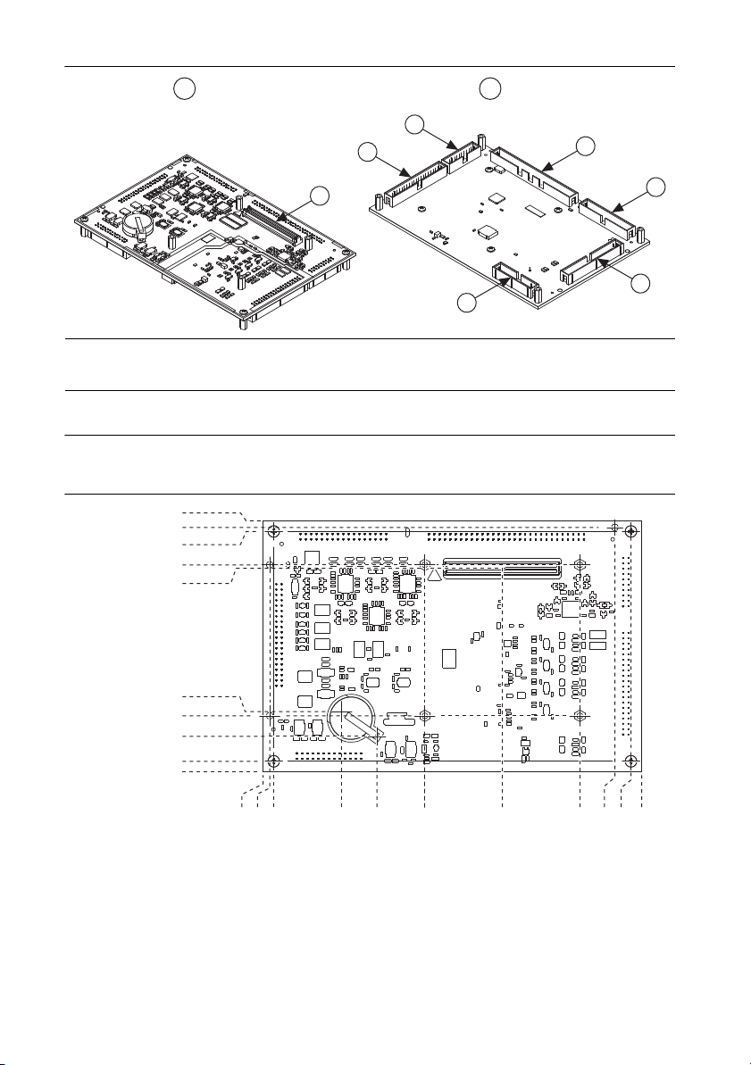
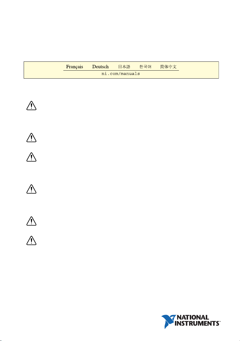
Figure 1. NI 9683 Parts Locator Diagram
1
2
7
5
9
3
4
6
8
1 Primary Side
2 Secondary Side
3 LVTTL DIO
4 Sourcing DI
5 Sinking DO and Relay Control DO
6 Half-bridge DO
Dimensions
Figures 2 through 4 show dimensional drawings of the NI 9683.
Figure 2. NI 9683 Primary Side Dimensions in Millimeters (Inches)
114.3 (4.500)
111.1 (4.374)
109.22 (4.300)
93.32 (3.674)
91.67 (3.609)
23.57 (0.928)
21.59 (0.850)
11.81 (0.465)
0.00 (0.000)
–5.08 (–0.200)
0.00 (0.000)
–5.08 (–0.200)
–1.88 (–0.074)
32.26 (1.270)
49.05 (1.931)
71.76 (2.825)
7 Simultaneous AI
8 Scanned AI and AO
9 sbRIO Mezzanine Connector
108.59 (4.275)
145.39 (5.724)
162.05 (6.380)
169.67 (6.680)
174.75 (6.880)
2 | ni.com | NI 9683 User Guide and Specifications
Page 3
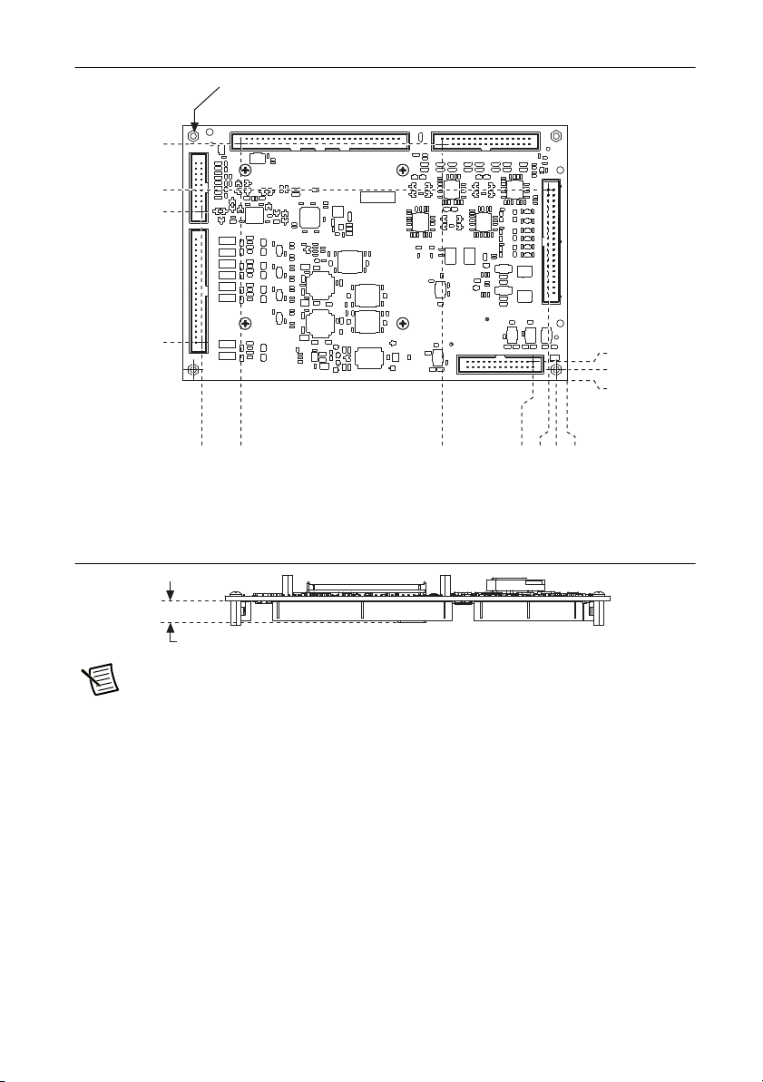
Figure 3. NI 9683 Secondary Side Dimensions in Millimeters (Inches)
105.46 (4.152)
84.12 (3.312)
73.66 (2.900)
12.70 (0.500)
165.91 (6.532)
53.34 (2.100)
10.92 (0.430)
147.32 (5.800)
3.76 (0.148)
0.00 (0.000)
–5.08 (–0.200)
3.76 (0.148)
0 (0.000)
–5.08 (–0.200)
11x Ø 3.30 (0.130)
9.98 (0.393)
Figure 4. NI 9683 Maximum Height of Components in Millimeters (Inches)
Note For more information about the dimensions of the NI 9683, including
two-dimensional drawings and three-dimensional models, go to
dimensions
.
NI 9683 User Guide and Specifications | © National Instruments | 3
ni.com/
Page 4
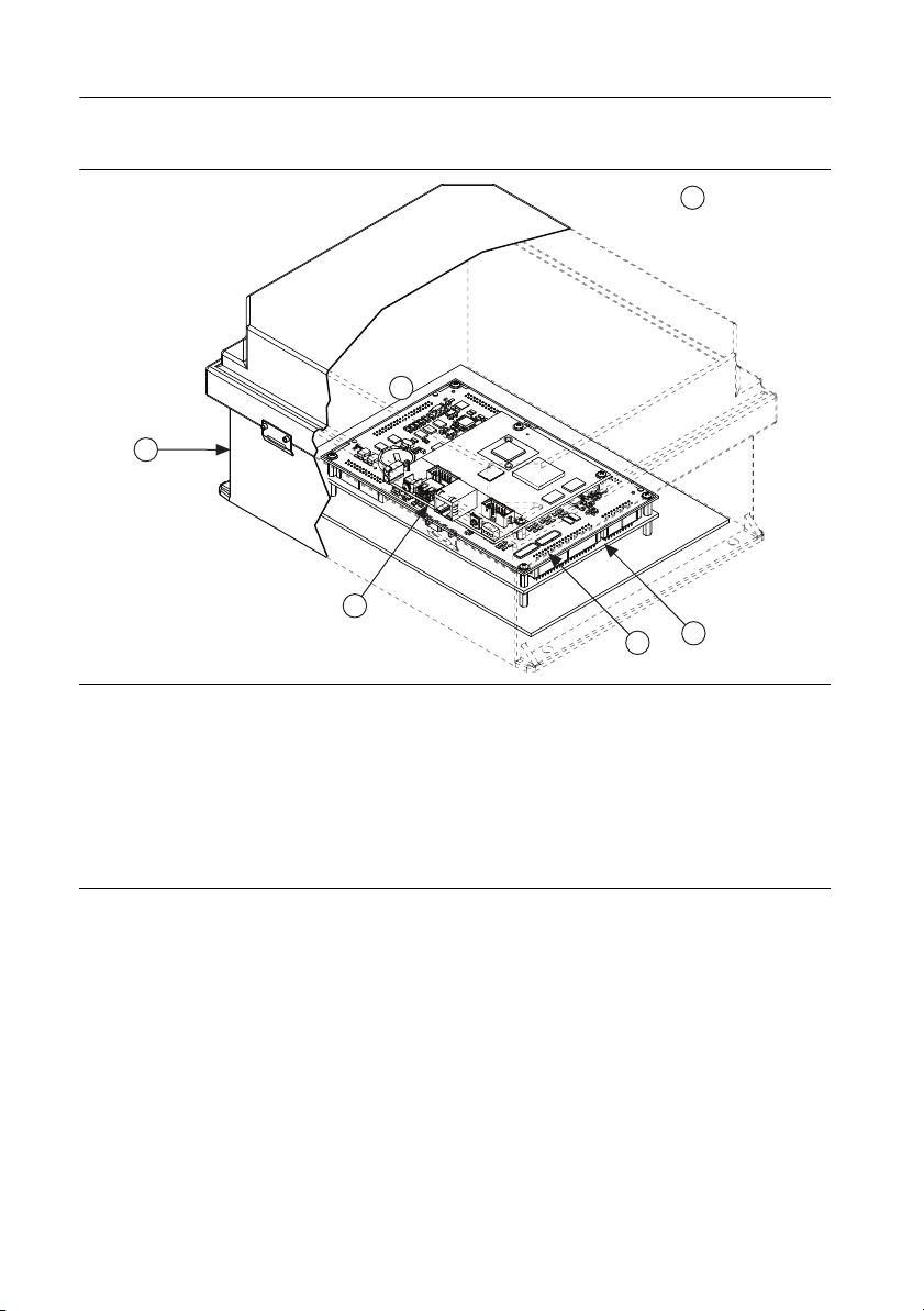
Typical NI 9683 System
Figure 5 shows a typical NI 9683 system.
Figure 5. Typical NI 9683 System
6
5
1
2
4
3
1 Enclosure. The NI 9683 must be installed inside a suitable enclosure.
2 NI sbRIO-9605/9606. Use the NI 9683 with only NI sbRIO-9605/9606 sbRIO devices.
3 NI 9683.
4 Interface board. The NI 9683 specifications assume direct board-to-board connections. Refer the Selecting
a Wire Gauge for Relay Control Digital Outputs section for information about designing ribbon cables to
meet the relay control DO specifications on the NI 9683.
5 Local ambient temperature location. The local ambient temperature is the operating temperature of the
NI 9683 inside the enclosure. Refer to the Environmental section for more information about the operating
temperature.
6 Ambient temperature location. The ambient temperature is the operating temperature outside of the
enclosure. Refer to the Environmental section for more information about the operating temperature.
4 | ni.com | NI 9683 User Guide and Specifications
Page 5
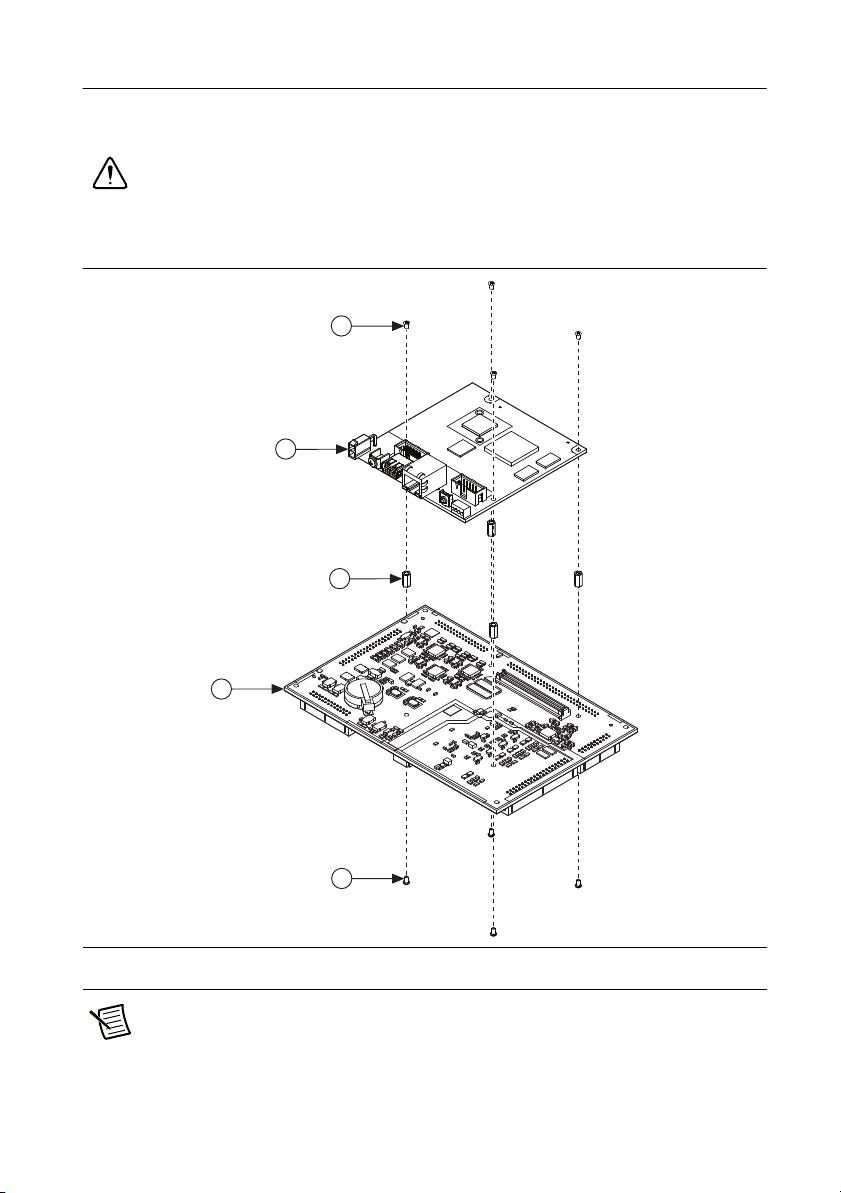
Mating the NI 9683 to the NI sbRIO-9605/9606
Figure 6 shows how to mate the NI 9683 to the NI sbRIO-9605/9606. Ensure that the
NI sbRIO-9605/9606 is powered off before connecting the NI 9683.
Caution You must use the standoffs specified below when mating the NI 9683 to
the NI sbRIO-9605/9606 to properly seat the sbRIO mezzanine connectors and
prevent damaging the device.
Figure 6. Mating the NI 9683 to the NI sbRIO-9605/9606
1
2
3
4
1 4-40 × 0.250 in. Screw (×8)
2 NI sbRIO-9605/9606
Note The screws include a nylon patch to prevent them from loosening when
subject to vibration. NI recommends using a 3/16 in. socket and Phillips screwdriver
when mating the NI 9683 to the NI sbRIO-9605/9606 to ensure the screw installs in
the standoff correctly.
1
3 4-40 × 0.380 in. Standoff (×4)
4 NI 9683
NI 9683 User Guide and Specifications | © National Instruments | 5
Page 6
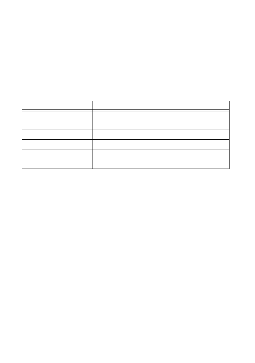
Connecting the NI 9683
The NI 9683 provides connections for 16 simultaneous analog input channels, 8 scanned analog
input channels, 8 analog output channels, 28 sourcing digital input channels, 14 half-bridge
digital output channels, 24 sinking digital output channels, 4 relay control digital output
channels, and 32 LVTTL digital input/output channels.
Table 7 lists and describes the connectors on the NI 9683 and the part number and manufacturer
of each connector. Refer to the manufacturer for information about using and matching these
connectors.
Figure 7. NI 9683 Connector Descriptions
Connector Description Recommended Mating Connector
Simultaneous AI 40-position header On-Shore Technology, Inc. (SH2-40G-PT)
Scanned AI, AO 20-position header On-Shore Technology, Inc. (SH2-20G-PT)
Sourcing DI 34-position header On-Shore Technology, Inc. (SH2-34G-PT)
Sinking DO, Relay Control DO 40-position header On-Shore Technology, Inc. (SH2-40G-PT)
Half-Bridge DO 26-position header On-Shore Technology, Inc. (SH2-26G-PT)
LVTTL DIO 60-position header On-Shore Technology, Inc. (SH2-60G-PT)
6 | ni.com | NI 9683 User Guide and Specifications
Page 7
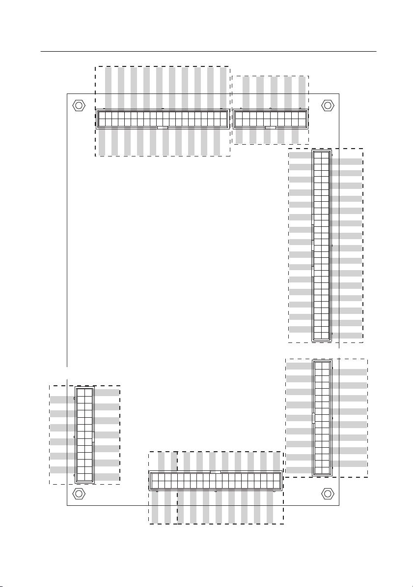
Figure 8 shows the NI 9683 pin assignments.
Figure 8. NI 9683 Pin Assignments
AI14–
AI15–
4 3
21
AI14+
AI15+
AI12–
AI13–
8
65
7
AI12+
AI13+
AI11–
10
9
AI11+
Simultaneous AI
AI6–
AI7–
AI8–
AI9–
AI10–
18
161412
20
17
151311
19
AI6+
AI7+
AI8+
AI9+
AI10+
AI5–
AI5+
AI4–
AI4+
AI1–
AI2–
AI3–
28
262422
30
27
252321
29
AI1+
AI2+
AI3+
AI0–
31
AI0+
CS COM
CS COM
363432
33
35
CS COM
CS COM
CS COM
CS COM
38
40
37
39
CS COM
CS COM
Scanned AI & AO
AO6
AO7
AI6
AO0
AO2
GND
AO4
10
8
642
7
531
9
AI7
AO1
AO3
GND
AO5
AI4
AI5
GND
161412
151311
GND
+3.3 V
+3.3 V
DIO 31
DIO 30
GND
DIO 27
DIO 26
GND
DIO 23
DIO 22
GND
DIO 19
DIO 18
GND
DIO 15
DIO 14
DIO 13
DIO 12
DIO 11
DIO 10
DIO 9
DIO 8
DIO 7
DIO 6
DIO 5
DIO 4
DIO 3
DIO 2
DIO 1
DIO 0
AI2
18
17
AI3
AI0
20
19
AI1
LVTTL
1
3
5
7
10
9
12
11
14
13
16
15
18
17
20
19
22
21
24
23
26
25
28
27
30
29
32
31
34
33
36
35
38
37
40
39
42
41
44
43
46
45
48
47
50
49
52
51
54
53
56
55
58
57
60
59
2
GND
4
GND
6
GND
8
DIO 29
DIO 28
GND
DIO 25
DIO 24
GND
DIO 21
DIO 20
GND
DIO 17
DIO 16
GND
GND
GND
GND
GND
GND
GND
GND
GND
GND
GND
GND
GND
GND
GND
GND
Half-Bridge
DO0
DO1
DO2
DO3
DO4
DO5
DO6
GND
GND
GND
GND
GND
Vex t
DO
26
24
22
20
18
16
14
12
10
8
6
4
2
Sourcing DI
1
NC
VI P1
DI P1.13
DI P1.11
DO20
DO18
3
579
4
6
DO21
DO19
DO22
1
2
DO23
DI P1.9
DI P1.7
DI P1.5
DI P1.3
DI P1.1
DI P0.13
DI P0.11
DI P0.9
DI P0.7
DI P0.5
DI P0.3
DI P0.1
VI P0
25
GND
23
GND
21
GND
19
GND
17
GND
15
GND
13
DO7
11
DO8
9
DO9
7
DO10
5
DO11
3
DO12
1
DO13
Relay
Control
DO
DO2+
DO1+
DO0+
37 38
3940
DO2–
DO1–
DO0–
Sinking DO
DO8
GND
DO6
DO4
DO2
DO0
NC
NC
DO3+
NC
23
252729
NC
DO1
21
24
262830
22
DO9
GND
DO7
DO5
DO3
31
32
33
35 36
34
DO3–
DO12
DO10
151719
161820
DO13
DO11
13
14
GND
DO14
11
10
12
GND
DO15
DO16
8
DO17
2
NC
3
4
GND
5
6
DI P1.12
7
9
DI P1.10
9
10
DI P1.8
11
12
DI P1.6
13
14
DI P1.4
15
16
DI P1.2
17
18
DI P1.0
19
20
DI P0.12
21
22
DI P0.10
23
24
DI P0.8
25
26
DI P0.6
27
28
DI P0.4
29
30
DI P0.2
31
32
DI P0.0
33
34
GND
NI 9683 User Guide and Specifications | © National Instruments | 7
Page 8
Simultaneous Analog Input
NI 9683
Simultaneous AI+
Simultaneous AI–
Isolated
ADC
Voltage Source
+
–
NI 9683
Simultaneous AI+
Simultaneous AI–
Isolated
ADC
Voltage Source
+
–
The NI 9683 provides connections for 16 pseudo-differential analog input channels.
Each channel has an AI+ and AI- pin to which you can connect a voltage signal. AI- is internally
connected to the isolated ground reference through a high value resistor.
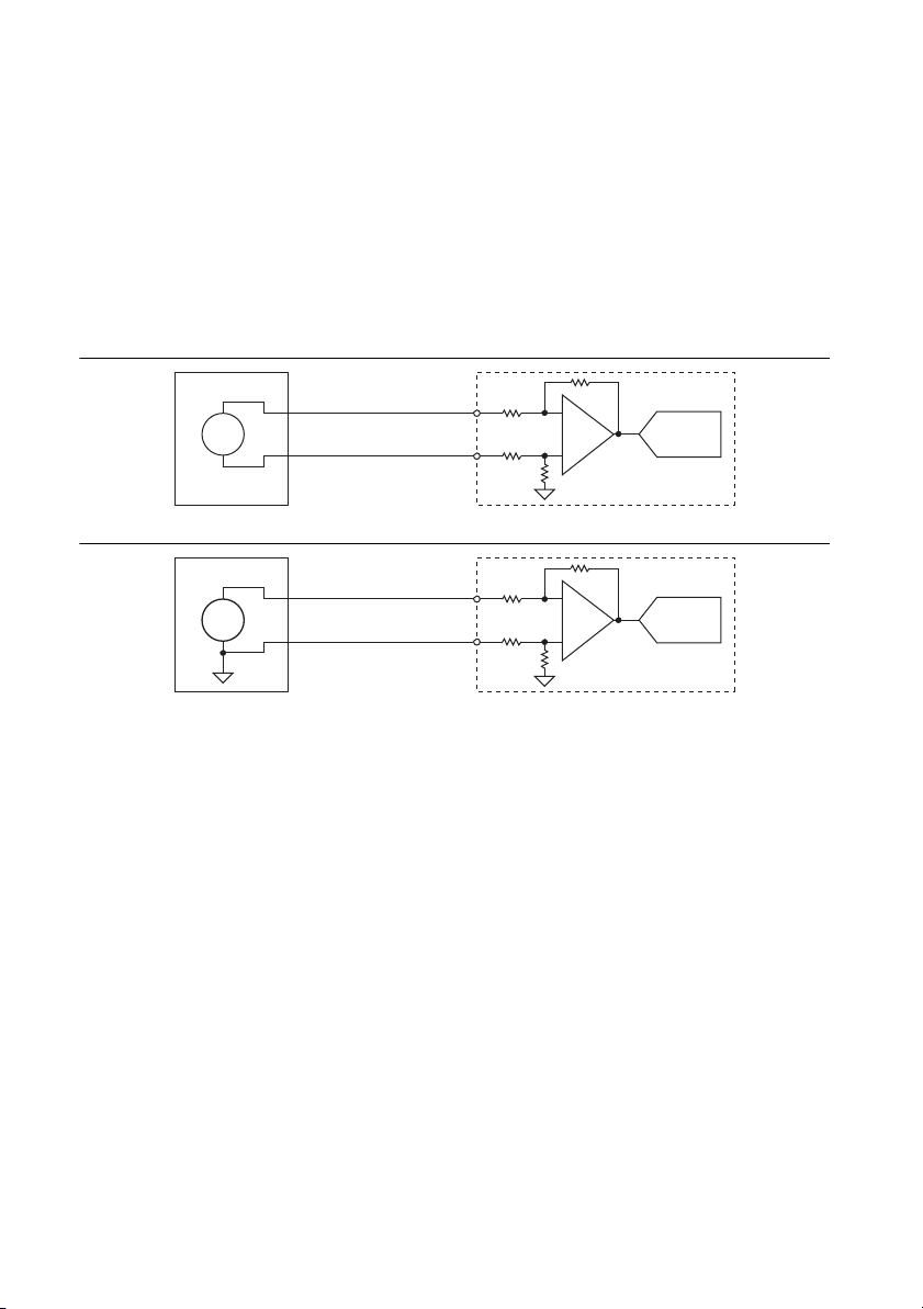
Connecting Differential and Single-Ended Voltage Signals to the NI 9683
You can connect grounded or floating signal sources to the NI 9683. Connect the positive
voltage signal to AI+ and the negative voltage signal to the AI-.
Figure 9. Connecting a Differential Voltage Signal to a Simultaneous AI Channel
Figure 10. Connecting a Single-Ended Voltage Signal to a Simultaneous AI Channel
NI 9683 Circuitry
The NI 9683 analog channels share a common ground that is isolated from other parts of the
board. The NI 9683 protects each channel from overvoltages. Refer to the Specifications section
for more information about overvoltage protection. The incoming analog signal on each channel
is buffered and conditioned by the differential amplifier and then sampled by a 12-bit ADC.
Each channel has an independent track-and-hold amplifier and ADC that allow you to sample
and convert all 16 channel simultaneously.
Connecting Current Sensors to the NI 9683
You can connect current sensors to the NI 9683 using a termination resistor to convert the current
measurement to a single-ended voltage measurement.
Connect the current sensor output to AI+ and the external power supply COM to the current
sensor common pin (CS COM) on the NI 9683.
8 | ni.com | NI 9683 User Guide and Specifications
Page 9
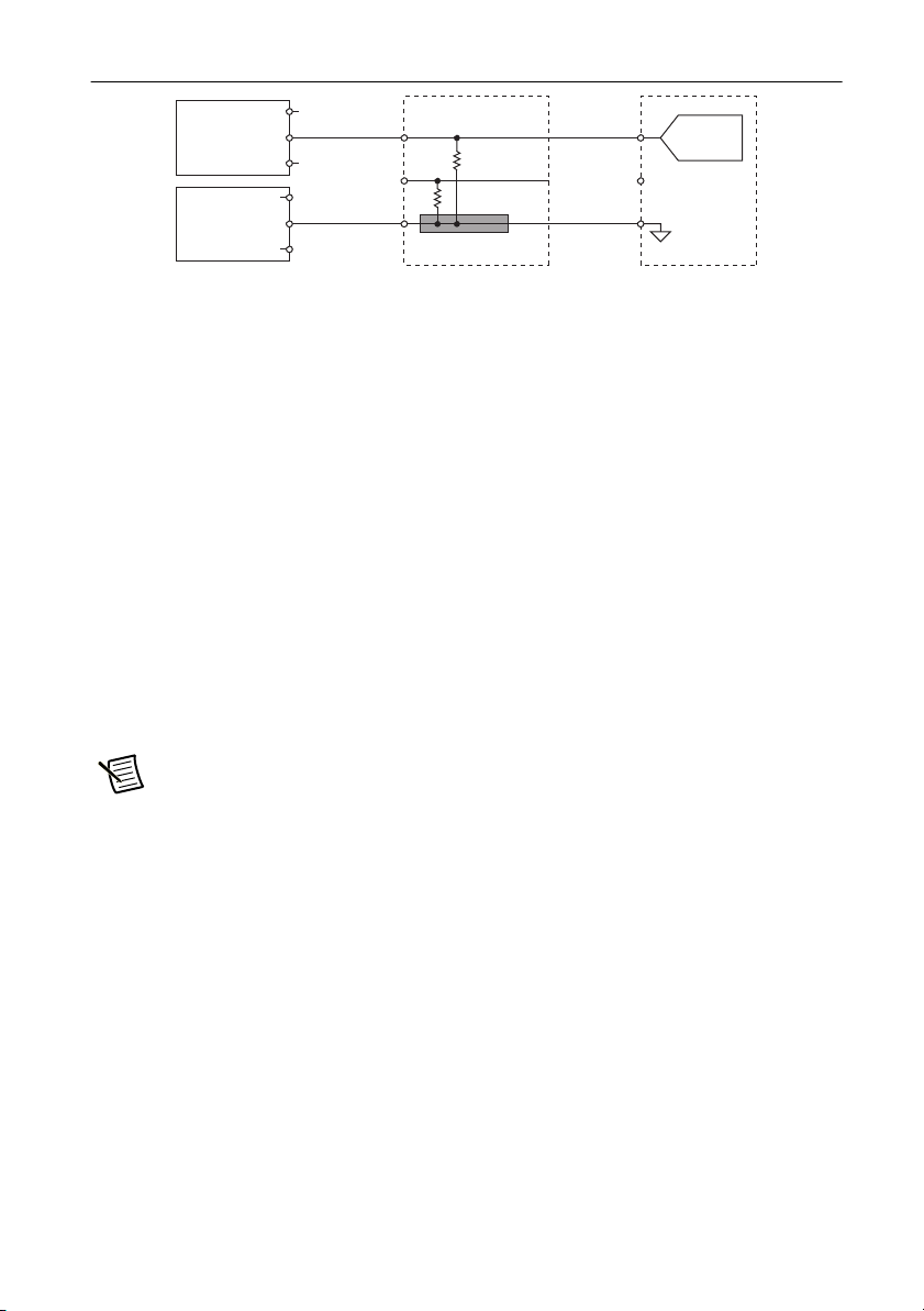
Figure 11. Connecting a Current Sensor to the NI 9683
NI 9683
Interface Board
Termination
Resistor
AI0+OUT
PS–
PS+
PS–
PS+
AI1+
CS COMCOM
Isolated
ADC
Current
Sensor
External
Powe r
Supply
R
max
5V
I_peak
max
--------------------------=
R
max
5V
0.07A
-------------- 71Ω==
To avoid the affect of common mode impedance on the measurement, connect one end of all the
termination resistors to a single, small plane. Then have a single connection from the plane to
the CS COM pin of the NI 9683.
The NI 9683 simultaneous analog inputs have ±10 V and ±5 V input ranges that can
accommodate termination resistor values in a certain range, based on the sensor peak current.
Select the highest possible termination resistor to maximize the dynamic range of the analog
input. Refer to the Specifications section for more information about the analog input range. Use
the following equation to determine the maximum value for the terminal resistor based on the
sensor peak current.
For a current sensor with a peak output current of 70 mA, the maximum termination resistor that
can be used with the NI 9683 is as follows:
Note Using the ±5 V input range can reduce the power dissipation on the
termination resistor by 50% when compared to the power dissipation of the ±10 V
input range.
Scanned Analog Input (Monitoring)
The NI 9683 provides connections for 8 single-ended scanned analog input channels.
Each channel has an AI pin to which you can connect a voltage signal. Scanned analog input and
scanned analog output channels share four GND pins on the dedicated 20-position connector.
NI 9683 User Guide and Specifications | © National Instruments | 9
Page 10

Figure 12. Connecting Single-Ended Voltage Signals to the Scanned Analog Inputs
NI 9683
ADCMUX
Scanned AI0
.
.
.
Scanned AI7
GND
Voltage Source
+
–
+
–
Scanned Analog Inputs Accuracy and Bandwidth
Use signal sources with an output impedance of less than 2 kΩ to ensure specified performance.
Large source impedances add to the input resistor inside the NI 9683, which results in increased
settling time and decreases the accuracy of the measurement. Increased input impedance also
results in a decrease of the -3 dB bandwidth.
Half-Bridge Digital Output
The NI 9683 provides connections for 14 half-bridge digital output channels.
Each channel has an half-bridge DO pin to which you can connect a digital input device. An
external power supply referenced to ground of the board must be connected to V
Figure 13. Connecting a Digital Device to a Half-Bridge DO Channel
.
ext
The NI 9683 has push-pull half-bridge digital outputs, meaning the NI 9683 can sink or source
current. When the channel is ON, the half-bridge DO pin is driven to the external power supply
minus a voltage drop due to the sourced current. When the channel is turned OFF, the half-bridge
DO pin is driven to ground plus a voltage drop due to the sinked current.
10 | ni.com | NI 9683 User Guide and Specifications
Vext
100 Ω
Half-Bridge DO
GND
NI 9683
Note Make sure the devices you connect to the NI 9683 are compatible with the
Device
half-bridge digital output specifications. Use connections that match the output
impedance of the NI 9683 half-bridge outputs. Refer to the Specifications section for
information about output voltages.
Page 11

Sinking Digital Output
NI 9683
Sinking DO
Device
Vcc
The NI 9683 provides connections for 24 sinking digital output channels.
Each channel has a sinking DO pin to which you can connect a digital input device. Sinking DO
pins have dedicated current return pins, GND, which are referenced to the ground of the board.
Figure 14. Connecting a Digital Device to a Sinking DO Channel
The NI 9683 has current sinking digital outputs, meaning that the output pin is driven to ground
(GND) when the channel is ON.
Make sure the devices you connect to the NI 9683 are compatible with the output specifications.
Refer to the Specifications section for information about output voltages.
Increasing Current Drive
Each channel has a continuous output current of 20 mA. If you want to increase the output
current to a device, you can connect any number of channels together in parallel. For example,
if you want to drive 80 mA of current, connect DO<0..3> in parallel as shown in Figure 15. You
must turn all parallel channels on and off simultaneously so that the current on any single
channel cannot exceed the 20 mA rating.
Figure 15. Increasing the Current to a Device Connected to the NI 9683
NI 9683
Sinking DO0
Sinking DO1
Sinking DO2
Sinking DO3
20 mA
20 mA
20 mA
20 mA
GND
NI 9683 User Guide and Specifications | © National Instruments | 11
80 mA
Device
+
_
External
Power
Supply
Page 12

Relay Control Digital Output
NI 9683
Relay Control DO+
Relay Control DO–
VDC1
VDC2
VDC3
VCM
+
–
Load
Relay Control DO+
Relay Control DO–
+
–
Load
Relay Control DO+
Relay Control DO–
+
–
Load
+
–
The NI 9683 provides connections for four relay control digital output channels. Each channel
has a relay control DO+ and a current return pin, relay control DO-.
The NI 9683 has current sinking outputs, meaning the relay control DO+ is driven to relay
control DO- when the channel is ON.
You can connect industrial devices such as solenoids, actuators, relays, and lamps to the NI 9683.
Refer to Figure 16 for an illustration of how to connect devices to the NI 9683.
Figure 16. Connecting an Industrial Device to a Relay Control DO Channel
Note Ensure that all the relay control DO+/- pins are held within the safety voltage
levels. A maximum common mode voltage of 30 VDC is allowed at a relay control
DO+/- pin with respect to the GND of the NI 9683. Refer to the Safety section for
maximum voltages allowed for the relay control DO channels.
Note NI recommends using the appropriate cabling for the current return pins
based on the amount of current returned per each relay control DO- output. Refer to
the Specifications section for information about peak and continuous current limits
based on the update rate.
Make sure the devices you connect to the NI 9683 are compatible with the output specifications.
Refer to the Specifications section for information about output voltages.
12 | ni.com | NI 9683 User Guide and Specifications
Page 13

Protecting the Relay Control Digital Outputs from Flyback Voltages
If the NI 9683 is switching an inductive or energy-storing device such as a solenoid, motor, or
relay and the device does not have flyback protection, install a flyback diode.
Figure 17. Connecting a Flyback Diode to a Relay Control DO Channel
Flyback
Diode
External
+
Powe r
–
Supply
NI 9683
Relay Control DO+
Relay Control DO–
Inductive
Device
Selecting a Wire Gauge for Relay Control Digital Outputs
The relay control digital output is capable of sinking 8 A of inrush current for a period of 300 ms
on a 60 second cycle and 500 mA of continuous current. Each channel is functionally isolated
from the other channels and the rest of the board, meaning that each relay control digital output
has a dedicated current return pin.
When using cables, make sure the current rating of the cable is able to handle the expected
current for your application. For example, a typical 28 AWG flat ribbon cable is rated at 225 mA
of continuous current per wire. In order to use the relay control digital outputs at their maximum
current capability, cables within category 24 AWG or lower should be used.
Sourcing Digital Input
The NI 9683 provides connections for 28 simultaneously sampled digital input channels
separated in ports P0 and P1. Ports P0 and P1 are independently powered using separate power
supply pins, VI P0 and VI P1. This allows you to connect the DI to multivoltage systems.
The NI 9683 has sourcing inputs, meaning the DI sources current from the VI P0 or VI P1 to the
sinking output device.The NI 9683 internally limits current signals connected to DI.
Each channel has a DI pin to which you can connect a digital input signal. The supply pins, VI P0
and VI P1, are referenced to the ground of the board. The DI operates in the low range or high
range based on the VI P0 or VI P1 voltage. Refer to the Specifications section for more
information about the low range and high range.
You can only connect 3-wire sinking-output devices to the NI 9683. Connect the sinking-output
device to the DI pin and the external power supply lead to the VI P0 or VI P1.
NI 9683 User Guide and Specifications | © National Instruments | 13
Page 14

Figure 18. Connecting a Digital Device to a Sourcing DI Channel
User
Board
NI sbRIO-9605/6
FPGA
DIO0
DIO31
.
.
.
NI 9683
Z0 = 55 Ω
Z
0 = 55 Ω
Z
0 = 55 Ω
Z
0 = 55 Ω
VI P0/VI P1
Sinking-Output
External
Powe r
Supply
+
–
Device
Sourcing DI
GND
4.32 kΩ
NI 9683
The NI 9683 channel registers ON when the sinking-output is in the ON range. The channel
registers as OFF when the sinking-output is in the OFF range. If no device is connected to the
sourcing DI, the channel registers as OFF. Refer to the Specifications section for more
information about the ON and OFF ranges of the sourcing DI.
Note NI recommends that you leave sourcing DI channels that are not used in your
application unconnected to lower power dissipation through the onboard pull-up
resistor.
LVTTL Digital Input/Output
The NI 9683 provides connections for 32 LVTTL digital input/output channels.
The NI 9683 LVTTL DIO channels connect directly to the FPGA DIO on the
NI sbRIO-9605/9606 and are unbuffered and unprotected. Refer to the Specifications section for
more information about the maximum current.
Caution Operating the LVTTL DIO outside the rated specifications may result in
permanent damage to the FPGA on NI sbRIO-9605/9606.
Figure 19. Connecting to the LVTTL DIO Channels
If overshoot and undershoot aberrations and signal integrity are concerns for your application,
use a single load per line that does not exceed 25 pF. For edge sensitive signals, use channels
DIO0 through DIO15 for better signal integrity and crosstalk performance since these channels
have an individual GND pin.
The LVTTL DIO channels on the NI 9863 are routed with a 55 Ω characteristic trace impedance.
Route all external circuitry with a similar impedance to ensure the best signal quality.
You should perform signal integrity measurements to test the effect of signal routing and cable
type on your application. To meet defined power-up states for outputs, use a pull-up or pull-down
resistor on the line.
14 | ni.com | NI 9683 User Guide and Specifications
Page 15

System Diagrams
Figures 20 and 21 show diagrams for interfacing digital and analog signals with the NI 9683.
Figure 20. Interfacing Digital Signals with the NI 9683
Relay +
+24V
+24V
+24V_COM
Supply
+24 VCC
+15V_HBDO
+15V_DI
Supply
+15 VCC
Relay –
Error Signal
Error
Monitor
+24 VDC IN
(13 V to 30 V)
GND (for power)
Top HB 1 IN
GND (for power)
IGBT Intelligent
Power Module
+24V_COM
+15V_DI
LED
+24V_COM
+15V_HBDO
+24V
Relay Control DO+
Relay Control DO–
VI P0 (5 V to 24 V)
Sourcing DI P0.0
Sinking DO
GND
GND
V
EXT (5 V to 24 V)
Half-Bride DO0
GND
GND
sbRIO Mezzanine Connector
9 V to 30 V
PS_COM
Digital GND (GND)
Isolation
Sourcing
DI0
NI 9683
NI sbRIO-9605/6
NI 9683 User Guide and Specifications | © National Instruments | 15
Page 16

+15 VCC
Bipolar Supply
+15V_CS
–15V_CS
CS_COM
+15V_CS
3
Figure 21. Interfacing Analog Signals with the NI 9683
Current
Sensor
RTermination
2
4 mA to 20 mA
Sensor
R
Termination
1
1
Simultaneous AI0+
Simultaneous AI0–
CS COM
Simultaneous AI1+
Simultaneous AI1–
ADC0
ADC1
Isolation
AO (Voltage)
GND aux
+24 VDC IN
+24V
+24V_COM
Supply
+24 VCC
1 Do not connect the AI- pin when using termination resistors.
2 Use a small plane shape for the current return point to reduce the common-mode impedance.
3 Do not connect CS COM to GND.
(13 V to 30 V)
GND (for power)
IGBT Intelligent
Power Module
Output
Sensor
Load
Simultaneous AI2+
Simultaneous AI2–
Scanned AI0
Scanned AI1
+
–
Scanned AI2
GND
AO0
GND
9 V to 30 V
PS_COM
.
.
.
sbRIO Mezzanine Connector
Digital GND (GND)
NI sbRIO-9605/6
ADC2
ADC
DAC
NI 9683
16 | ni.com | NI 9683 User Guide and Specifications
Page 17

Specifications
The following specifications are typical for the full operating temperature range unless otherwise
noted. Refer to the Environmental section for more information on operating temperatures.
Simultaneous Analog Input
Number of channels.......................................... 16
ADC resolution................................................. 12 bits
Input range
Typical ...................................................... ±5 V, ±10 V
Minimum .................................................. ±4.95 V, ±9.90 V
Common-mode range ....................................... ±10 V
Sample rate (per channel) ................................. 100 kS/s max
Accuracy
Nominal
Range (V)
Measurement Conditions
*
Percent of
Reading
(Gain Error)
Percent of
Range
(Offset Error)
±5 Maximum (-40 °C to 85 °C) 0.70% 0.28%
Typical (23 ° ±5 °C) 0.25% 0.12%
±10 Maximum (-40 °C to 85 °C) 0.70% 0.16%
Typical (23 ° ±5 °C) 0.25% 0.07%
AbsoluteAccuracy = Reading(GainError) + Range(OffsetError) + Noise
* Local ambient temperature. Refer to the Environmental section for more information about operating
temperatures.
†
Offset error includes the effect of INL.
Stability
Gain drift................................................... 15 ppm/°C
Offset drift ................................................ 15 µV/°C
Noise................................................................. 1.5 mV
rms
-3 dB bandwidth ............................................... 210 kHz
CMRR (f
= 60 Hz).......................................... 60 dB min
in
Input impedance
Differential................................................ 240 kΩ
Single-ended ............................................. 120 kΩ
Overvoltage protection ..................................... ±30 V max
†
NI 9683 User Guide and Specifications | © National Instruments | 17
Page 18

Scanned Analog Input (Monitoring)
Number of channels .......................................... 8
ADC resolution ................................................. 12 bits
Input range
Typical.......................................................0 V to 5 V
Minimum .................................................. 12 mV to 4.97 V
Sample rate (all channels) .................................1 kS/s max
Accuracy
Stability
Noise ................................................................. 0.5 mV
-3 dB bandwidth................................................ 130 kHz
Input impedance for channel ON ......................10 kΩ, 120 pF low pass filter
Input current for channel OFF .......................... 10 μA max
Overvoltage protection ..................................... ±30 V max
1
Measurement
Conditions
*
Percent of Reading
(Gain Error)
Percent of Range
(Offset Error)
‡
Maximum (-40 °C to 85 °C) 0.30% 0.23%
Typical (23 ° ±5 °C) 0.03% 0.03%
AbsoluteAccuracy = Reading(GainError) + Range(OffsetError) + Noise
*
Local ambient temperature. Refer to the Environmental section for more information about operating
temperatures.
†
Range equals 5 V.
‡
Offset error includes the effect of INL.
Gain drift...................................................3 ppm/°C
Offset drift.................................................3 µV/°C
rms
†
Analog Output (Set-Point)
Number of channels .......................................... 8
DAC resolution ................................................. 12 bits
Startup voltage .................................................. 0 V
1
With signal source impedance <2 kΩ. Refer to the Scanned Analog Input (Monitoring) section for more
information about the influence of source impedance over accuracy.
18 | ni.com | NI 9683 User Guide and Specifications
Page 19

Output range
Typical ...................................................... 0 V to 5 V
Minimum .................................................. 14 mV to 4.97 V
Current drive (per channel)............................... 4 mA max
Update rate........................................................ 1 kS/s min
Accuracy
Measurement Conditions
Percent of Reading
*
(Gain Error)
Percent of Range†
(Offset Error)
‡
Maximum (-40 °C to 85 °C) 0.33% 0.28%
Typical (23 ° ±5 °C) 0.06% 0.06%
AbsoluteAccuracy = OutputValue(GainError) + Range(OffsetError)
*
Local ambient temperature. Refer to the Environmental section for more information about operating
temperatures.
†
Range equals 5 V.
‡
Offset error includes the effect of INL.
Stability
Gain drift................................................... 3 ppm/°C
Offset drift ................................................ 3 µV/°C
Noise
1 MHz bandwidth ..................................... 2.5 mV
100 kHz bandwidth................................... 0.3 mV
rms
rms
Protection
Overvoltage .............................................. +15 V/-5 V max
Short-circuit .............................................. Indefinitely
Sourcing Digital Input
Number of channels.......................................... 28
Input type .......................................................... Sourcing
Input range........................................................ 0 V to 24 V
External power supply voltage range (VI P0, VI P1)
Low-range mode....................................... 3 V to 6 V
High-range mode ...................................... 10 V to 24 V
Not supported ........................................... 6 V to 10 V
Digital logic levels
Low-range mode
OFF state........................................... ≥1.8 V min
ON state ............................................ ≤1 V max
NI 9683 User Guide and Specifications | © National Instruments | 19
Page 20

High-range mode
OFF state........................................... ≥9.6 V min
ON state ............................................≤7.9 V max
1
Hold time
Setup time
.........................................................0 s
2
........................................................1 µs min
Update/transfer time ......................................... 3 µs max
Pull-up resistor .................................................. 4.32 kΩ
Overvoltage protection ..................................... ±30 V max
Sinking Digital Output
Number of channels .......................................... 24
Output type .......................................................Sinking
Startup voltage .................................................. Open
Output voltage (V
Continuous output current (IO)
on each channel................................................. 20 mA
Output impedance (RO)..................................... 6 Ω max
External power supply voltage range................ 0 V to 30 V
Maximum update time ...................................... 50 μs
Protection
Reversed-voltage ......................................None
Short-circuit .............................................. None
) ..........................................IO · R
O
O
Half-Bridge Digital Output
Number of channels .......................................... 14
Output type ....................................................... Sourcing/Sinking
Startup voltage .................................................. 0 V
Maximum continuous output current................ 10 mA
Output impedance ............................................. 100 Ω
External power supply voltage range (V
1
Hold time is the amount of time input signals must be stable after initiating a read from the NI 9683.
2
Setup time is the amount of time input signals must be stable before reading from the NI 9683.
20 | ni.com | NI 9683 User Guide and Specifications
)......5 V to 30 V
ext
Page 21

Digital logic levels
High (V
)
OH
Sourcing 0.1 mA............................... V
Sourcing 10 mA................................ V
- 0.01 V
ext
- 1.05 V
ext
Low (VOL)
Sinking 0.1 mA................................. 0.01 V
Sinking 10 mA.................................. 1.05 V
Minimum pulse-width ......................................500 ns
Maximum switching frequency
V
= 30 V, CL = 1 nF.............................. 100 kHz
ext
= 30 V, CL = 50 pF............................ 500 kHz
V
ext
1
1
The maximum switching frequency must be limited to 500 kHz, regardless of the supply voltage or the
capacitive load, in order to prevent output driver overstress.
NI 9683 User Guide and Specifications | © National Instruments | 21
Page 22

Figure 22. Maximum Switching Frequency Based on the Capacitive Load
Capacitive Load (nF)
8
18
16
14
12
10
6
4
2
5
10 25 50 100 200 300
Maximum Switching Frequency (kHz)
20
0
500
Vext = 5 V
Vext = 15 V
Vext = 30 V
Vext = 5 V
Vext = 15 V
Vext = 30 V
Supply Voltage (V)
30
25
20
15
10
5
10 25 50 100 200 300
Maximum Switching Frequency (ktHz)
35
5
500
CL = 0.47 nF
CL =
1 n
F
CL = 10 nF
Figure 23. Maximum Switching Frequency Based on the Supply Voltage
Propagation delay
V
= 5 V, CL = 50 pF..............................300 ns max
ext
> 15 V, CL = 50 pF............................100 ns max
V
ext
Protection
Overcurrent ............................................... None
Short-circuit .............................................. None
22 | ni.com | NI 9683 User Guide and Specifications
Page 23

Relay Control Digital Output
Relay control DO specifications assume the use of direct board-to-board connections to I/O
connectors on the NI 9683. Refer to the Selecting a Wire Gauge for Relay Control Digital
Outputs section for information about designing ribbon cables to meet the relay control DO
specifications on the NI 9683.
Number of channels.......................................... 4
Output type ....................................................... Sinking
Startup voltage .................................................. Open
External power supply voltage range ............... 0 V to 30 V
Continuous current ........................................... 500 mA
Maximum inrush current .................................. 8 A
Maximum inrush time ...................................... 300 ms
Turn ON rate
1
................................................... 1 operation per 60 s
Turn ON time.................................................... 6 ms max
Turn OFF time .................................................. 0.2 ms max
Protection
Reversed-voltage ...................................... None
Short-circuit .............................................. None
LVTTL Digital Input/Output
Number of DIO channels.................................. 32
Maximum tested current (per channel)............. 3 mA
Maximum total current (all lines) ..................... 96 mA
Note The performance of the LVTTL DIO lines is bound by the FPGA, signal
integrity, the applications timing requirements, and your design. For more
information on using DIO to connect to RMCs, go to
Info Code
1
Turn ON rate is the minimum time between inrush current events and is based on the maximum inrush
current over the maximum inrush time. You can turn OFF the relay control DO at any point during
operation.
RMCDIO.
NI 9683 User Guide and Specifications | © National Instruments | 23
ni.com/info and enter the
Page 24

Digital logic levels
Input low voltage, V
Input high voltage, V
Output high voltage, V
...............................0 V min, 0.8 V max
IL
............................. 2.0 V min, 3.465 V max
IH
OH
sourcing 3 mA...........................................2.7 V min, 3.3 V max
Output low voltage, V
OL
sinking 3 mA.............................................0.0 V min, 0.4 V max
Protection
Overvoltage............................................... None
Overcurrent ............................................... None
Short-circuit .............................................. None
Power Requirements
Power consumption from
NI Single-Board RIO device............................. 2 W max
Power-up time...................................................0.1 s
Safety
Maximum Voltage
Connect voltages that are within the following limits.
Relay control digital output
Relay control DO+ to
Relay control DO-.....................................0 VDC to 30 VDC
Relay control DO+/- to GND....................±30 VDC
Sinking digital output
DO-to-GND ..............................................±30 VDC
Simultaneous analog input, scanned analog input, analog output, sourcing digital input
Pin-to-pin or pin-to-GND ......................... ±30 VDC
Half-bridge digital output
-to-GND.............................................. 0 VDC to 30 VDC
V
ext
LVTTL digital input/output ..............................0 VDC to 3.465 VDC
Isolation Voltages
Simultaneous analog input
Channel-to-channel ................................... None
Channel-to-common
Continuous ........................................60 VDC, Measurement Category I
Withstand .......................................... 1,000 V
24 | ni.com | NI 9683 User Guide and Specifications
rms
Page 25

Measurement Category I is for measurements performed on circuits not directly connected to the
electrical distribution system referred to as MAINS voltage. MAINS is a hazardous live electrical
supply system that powers equipment. This category is for measurements of voltages from
specially protected secondary circuits. Such voltage measurements include signal levels, special
equipment, limited-energy parts of equipment, circuits powered by regulated low-voltage
sources, and electronics.
Caution Do not connect the NI 9683 to signals or use for measurements within
Measurement Categories II, III, or IV.
Environmental
Operating temperature (IEC 60068-2-1, IEC 60068-2-2)
Ambient temperature outside
a 12 in. × 10 in. × 6.34 in. enclosure
Ambient temperature with forced-air
cooling in an open environment
Note Visit ni.com/info and enter the Info Code sbRIOcooling for
information about NI sbRIO operating temperatures.
Storage temperature
(IEC 60068-2-1, IEC 60068-2-2) ..................... - 40 °C to 85 °C
Operating humidity (IEC 60068-2-56) ............. 10% to 90% RH, noncondensing
Storage humidity (IEC 60068-2-56)................. 5% to 95% RH, noncondensing
Pollution Degree (IEC 60664).......................... 2
Maximum altitude............................................. 2,000 m
Indoor use only.
1
....... - 40 °C to 50 °C
1
.............. -40 °C to 70 °C
Physical Characteristics
Weight............................................................... 153 g
Environmental Management
NI is committed to designing and manufacturing products in an environmentally responsible
manner. NI recognizes that eliminating certain hazardous substances from our products is
beneficial to the environment and to NI customers.
For additional environmental information, refer to the Minimize Our Environmental Impact web
ni.com/environment. This page contains the environmental regulations and
page at
directives with which NI complies, as well as other environmental information not included in
this document.
1
Ensure that the local ambient temperature of the NI 9863 is -40 °C to 85 °C. Measure the local ambient
temperature by placing thermocouples on both sides of the PCB, 5 mm (0.2 in.) from the board surface.
NI 9683 User Guide and Specifications | © National Instruments | 25
Page 26

Waste Electrical and Electronic Equipment (WEEE)
⬉ᄤֵᙃѻક∵ᶧࠊㅵ⧚ࡲ⊩ ˄Ё
RoHS
˅
Ёᅶ᠋
National Instruments
ヺড়Ё⬉ᄤֵᙃѻકЁ䰤ࠊՓ⫼ᶤѯ᳝ᆇ⠽䋼ᣛҸ
(RoHS)
DŽ݇Ѣ
National Instruments
Ё
RoHS
ড়㾘ᗻֵᙃˈ䇋ⱏᔩ
ni.com/
environment/rohs_china
DŽ
(For information about China RoHS compliance,
go to
ni.com/environment/rohs_china
.)
EU Customers At the end of the product life cycle, all products must be sent to
a WEEE recycling center. For more information about WEEE recycling centers,
National Instruments WEEE initiatives, and compliance with WEEE Directive
2002/96/EC on Waste and Electronic Equipment, visit
.
weee
ni.com/environment/
Battery Replacement and Disposal
Battery Directive This device contains a long-life coin cell battery. If you need
Cd/Hg/Pb
to replace it, use the Return Material Authorization (RMA) process or contact an
authorized National Instruments service representative. For more information
about compliance with the EU Battery Directives 2006/66/EC about Batteries
and Accumulators and Waste Batteries and Accumulators, visit
environment/batterydirective
.
ni.com/
Where to Go for Support
The National Instruments Web site is your complete resource for technical support. At
ni.com/support you have access to everything from troubleshooting and application
development self-help resources to email and phone assistance from NI Application Engineers.
National Instruments corporate headquarters is located at 11500 North Mopac Expressway,
Austin, Texas, 78759-3504. National Instruments also has offices located around the world to
help address your support needs. For telephone support in the United States, create your service
request at
ni.com/support and follow the calling instructions or dial 512 795 8248. For
telephone support outside the United States, visit the Worldwide Offices section of ni.com/
niglobal
to access the branch office Web sites, which provide up-to-date contact information,
support phone numbers, email addresses, and current events.
26 | ni.com | NI 9683 User Guide and Specifications
Page 27

Refer to the NI Trademarks and Logo Guidelines at ni.com/trademarks for more information on National Instruments trademarks. Other
product and company names mentioned herein are trademarks or trade names of their respective companies. For patents covering National
Instruments products/technology, refer to the appropriate location: Help»Patents in your software, the patents.txt file on your media, or the
National Instruments Patents Notice at ni.com/patents. You can find information about end-user license agreements (EULAs) and third-party
legal notices in the readme file for your NI product. Refer to the Export Compliance Information at ni.com/legal/export-compliance
for the National Instruments global trade compliance policy and how to obtain relevant HTS codes, ECCNs, and other import/export data.
© 2012–2013 National Instruments. All rights reserved.
375960B-01 Feb13
 Loading...