

Page 1

USER GUIDE AND SPECIFICATIONS
NI 9144
Deterministic Ethernet Expansion Chassis for C Series Modules
Contents
Introduction.............................................................................................2
Safety Guidelines .................................................................................... 3
Safety Guidelines for Hazardous Locations .................................... 3
Special Conditions for Hazardous Locations Use
in Europe................................................................................ 4
Special Conditions for Marine Applications ................................... 4
Mounting the NI 9144 Chassis................................................................ 4
Mounting the NI 9144 Chassis on a Panel....................................... 6
Mounting the Chassis on a DIN Rail ...............................................8
Connecting the NI 9144 Chassis to a Network ....................................... 9
Understanding LED Indications.............................................................. 10
POWER LED...................................................................................10
FPGA LED—Open FPGA Mode Only ........................................... 10
RUN and ERR LEDs ....................................................................... 10
Resetting the NI 9144 Network Configuration ....................................... 12
Safe-State Outputs................................................................................... 12
Slave Timing Modes ............................................................................... 12
Updating your Firmware ......................................................................... 12
Using the NI 9144 with an EtherCAT Third-Party Master..................... 13
Using AoE/SDO .............................................................................. 13
Using CoE/SDO............................................................................... 13
Specifications .......................................................................................... 14
Network ...........................................................................................14
Power Requirements ........................................................................ 14
Physical Characteristics ................................................................... 14
Safety Voltages ................................................................................14
Hazardous Locations........................................................................ 15
Environmental..................................................................................15
Shock and Vibration ........................................................................16
Cabling............................................................................................. 16
Safety Standards .............................................................................. 17
Page 2

Electromagnetic Compatibility.........................................................17
CE Compliance.................................................................................18
Online Product Certification.............................................................18
Environmental Management ............................................................18
Appendix A..............................................................................................19
Vendor Extensions to the Object Dictionary....................................19
Supported C Series Modules ............................................................20
C Series Modules with No Configurable Options.....................20
NI 9201/9221.............................................................................21
NI 9203......................................................................................24
NI 9205/9206.............................................................................28
NI 9211......................................................................................31
NI 9213......................................................................................32
NI 9215......................................................................................34
NI 9217......................................................................................35
NI 9219......................................................................................38
NI 9233......................................................................................49
NI 9234......................................................................................52
NI 9237......................................................................................55
NI 9229/9239.............................................................................58
NI 9263......................................................................................60
NI 9264......................................................................................61
NI 9265......................................................................................62
NI 9401......................................................................................63
NI 9403......................................................................................63
NI 9476......................................................................................64
Where to Go for Support .........................................................................65
Introduction
This document describes how to connect the NI 9144 chassis to a network,
how to use the NI 9144 chassis features, and contains the NI 9144 chassis
specifications. The NI 9144 is a slave device and requires a compliant
EtherCAT Master and network to function.
NI 9144 User Guide and Specifications 2 ni.com
Page 3
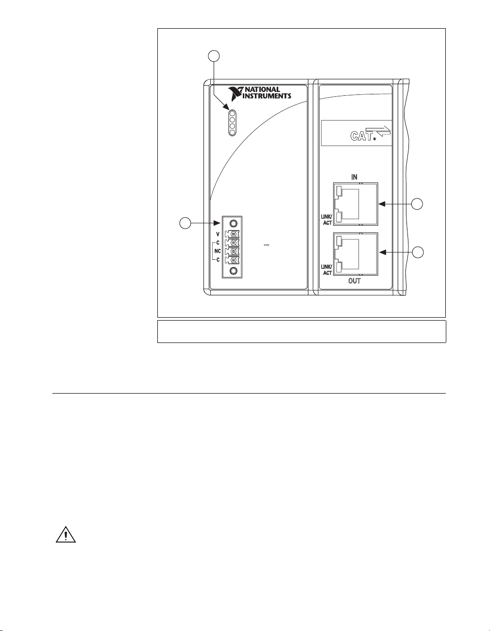
1
INPUT
9-30 V
20 W MAX
NI 9144
POWER
FPGA
RUN
ERR
4
Ether
2
3
1LEDs
2IN Port
3OUT Port
4 Power Connector
Figure 1. NI 9144 Chassis
Safety Guidelines
Operate the NI 9144 chassis only as described in this user guide.
Safety Guidelines for Hazardous Locations
The NI 9144 chassis is suitable for use in Class I, Division 2, Groups A, B,
C, D, T4 hazardous locations; Class 1, Zone 2, AEx nA IIC T4 and Ex nA
IIC T4 hazardous locations; and nonhazardous locations only. Follow these
guidelines if you are installing the NI 9144 chassis in a potentially
explosive environment. Not following these guidelines may result in
serious injury or death.
Caution Do not disconnect the power supply wires and connectors from the chassis unless
power has been switched off.
© National Instruments Corporation 3 NI 9144 User Guide and Specifications
Page 4

Caution Substitution of components may impair suitability for Class I, Division 2.
Caution For Zone 2 applications, install the system in an enclosure rated to at least IP 54
as defined by IEC 60529 and EN 60529.
Special Conditions for Hazardous Locations Use in Europe
This equipment has been evaluated as Ex nA IIC T4 equipment under
DEMKO Certificate No. 07 ATEX 0626664X. Each chassis is marked
II 3G and is suitable for use in Zone 2 hazardous locations, in ambient
temperatures of –40 ≤ Ta ≤ 70 °C.
Special Conditions for Marine Applications
Some chassis are Lloyd’s Register (LR) Type Approved for marine
applications. To verify Lloyd’s Register certification, visit
certification
Register mark on the chassis.
and search for the LR certificate, or look for the Lloyd’s
Mounting the NI 9144 Chassis
You can mount the chassis in any orientation on a 35 mm DIN rail or on a
panel. Use the DIN rail mounting method if you already have a DIN rail
configuration or if you need to be able to quickly remove the chassis. Use
the panel mount method for high shock and vibration applications.
ni.com/
Caution Your installation must meet the following requirements for space and cabling
clearance:
• Allow 25.4 mm (1 in.) on the top and the bottom of the chassis for air circulation.
• Allow 50.8 mm (2 in.) in front of C Series I/O modules for cabling clearance for
common connectors, such as the 10-terminal, detachable screw terminal connector, as
shown in Figure 2.
NI 9144 User Guide and Specifications 4 ni.com
Page 5
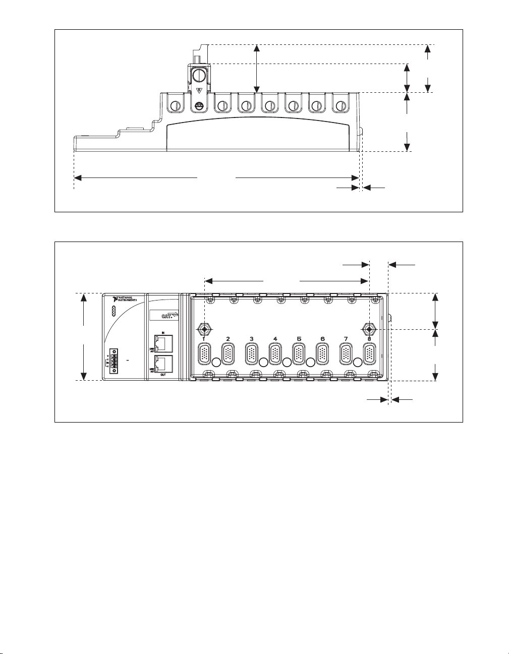
87.3 mm
(3.44 in.)
POWER
FPGA
RUN
ERR
INPUT
9-30 V
20 W MAX
Ether
NI 9144
Cabling Clearance
50.8 mm (2.00 in.)
29.0 mm
(1.14 in.)
286.4 mm
(11.28 in.)
3.2 mm
(0.13 in.)
Figure 2. NI 9144 Chassis, Bottom View with Dimensions
19.0 mm
165.1 mm
(6.5 in.)
(0.75 in.)
48.4 mm
(1.9 in.)
58.9 mm
(2.32 in.)
36.4 mm
(1.43 in.)
51.7 mm
(2.04 in.)
2.9 mm
(0.12 in.)
Figure 3. NI 9144 Chassis, Front View with Dimensions
© National Instruments Corporation 5 NI 9144 User Guide and Specifications
Page 6

44.069 mm
(1.74 in.)
25.078 mm
(0.99 in.)
44.125 mm
(1.74 in.)
63.178 mm
(2.49 in.)
Figure 4. NI 9144 Chassis, Side View with Dimensions
The following sections contain mounting method instructions. Before
using any of these mounting methods, record the serial number from the
back of the chassis. After the chassis is mounted, you will not be able to
read the serial number.
Caution Remove any C Series I/O modules from the chassis before mounting it.
Mounting the NI 9144 Chassis on a Panel
Use the NI 9905 panel mount kit to mount the NI 9144 chassis on a flat
surface. To use the NI 9905 panel mount kit, complete the following steps:
1. Fasten the chassis to the panel mount kit using a number 2 Phillips
screwdriver and two M4 × 16 screws. National Instruments provides
these screws with the panel mount kit. You must use these screws
because they are the correct depth and thread for the panel.
20.320 mm
(0.8 in.)
NI 9144 User Guide and Specifications 6 ni.com
Page 7
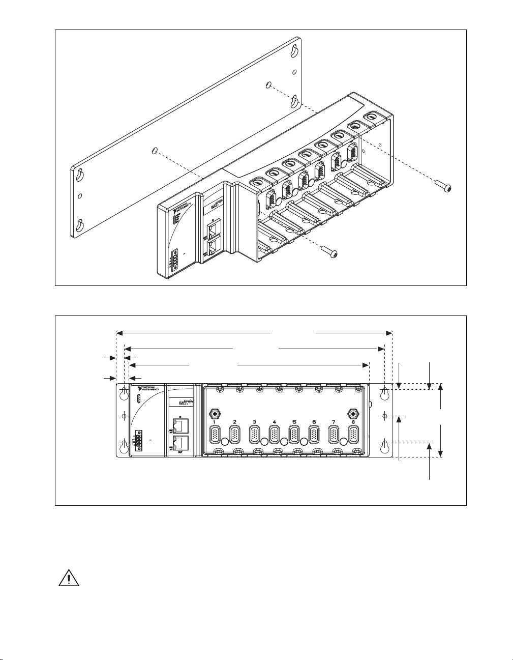
9.525 mm
(0.38 in.)
15.491 mm
(0.61 in.)
NI 9144
Ether
INPUT
9-30 V
20 W MAX
Figure 5. Installing the Panel Mount Accessory on the NI 9144 Chassis
330.200 mm
311.150 mm
286.634 mm
(11.28 in.)
INPUT
9-30 V
20 W MAX
NI 9144
Ether
POWER
FPGA
RUN
ERR
(12.25 in.)
(13 in.)
31.750 mm
(1.25 in.)
63.500 mm
88.138 mm
(3.47 in.)
(2.5 in.)
Figure 6. Dimensions of NI 9144 Chassis with Panel Mount Accessory Installed
2. Fasten the NI 9905 panel to the wall using the screwdriver and screws
that are appropriate for the wall surface.
Caution Remove any C Series I/O modules from the chassis before removing it from the
panel.
© National Instruments Corporation 7 NI 9144 User Guide and Specifications
Page 8
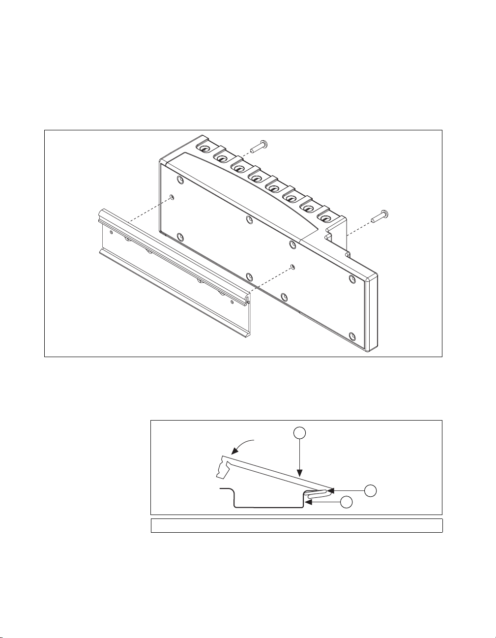
Mounting the Chassis on a DIN Rail
Use the NI 9915 DIN rail mount kit if you want to mount the chassis on a
DIN rail. You need one clip for mounting the chassis on a standard 35 mm
DIN rail. Complete the following steps to mount the chassis on a DIN rail:
1. Fasten the DIN rail clip to the chassis using a number 2 Phillips
screwdriver and two M4 × 16 screws. National Instruments provides
these screws with the DIN rail mount kit.
Figure 7. Installing the DIN Rail Clip on the NI 9144 Chassis
2. Insert one edge of the DIN rail into the deeper opening of the DIN rail
clip, as shown in Figure 8.
1
2
3
1 DIN Rail Clip 2 DIN Rail Spring 3 DIN Rail
Figure 8. One Edge of the DIN Rail Inserted in a Clip
NI 9144 User Guide and Specifications 8 ni.com
Page 9
3. Press down firmly on the chassis to compress the spring until the clip
locks in place on the DIN rail.
Caution Remove any C Series I/O modules from the chassis before removing the chassis
from the DIN rail.
Connecting the NI 9144 Chassis to a Network
NI recommends that you install a private network segment for your
deterministic Ethernet expansion devices. Slave devices cause network
flooding on a standard network. Non-EtherCAT frames jeopardize the
system performance and determinism on an EtherCAT network. Refer to
the EtherCAT Technology Group Web site at
more information.
The following devices are required to connect the NI 9144 chassis to a
network successfully: a host computer, a supported LabVIEW Real-Time
1
target
with the NI-Industrial Communications for EtherCAT software
driver installed on it, and an NI 9144 slave device.
To have your LabVIEW target establish a connection with the NI 9144
chassis, connect the secondary port of the LabVIEW Real-Time target to
the NI 9144 IN port. Use a standard Category 5 (CAT-5) or better Ethernet
cable. Use the NI 9144 OUT port to connect to other NI 9144 chassis and
slave devices on the same segment.
www.ethercat.org, for
Once the connection is established, install the NI-Industrial
Communications for EtherCAT software on the host computer and then use
Measurement and Automation Explorer (MAX) to install the NI-Industrial
Communications for EtherCAT driver on the target.
Caution To update your firmware on the NI 9144 chassis, refer to the Updating your
Firmware section of this user guide.
Caution To prevent data loss and to maintain the integrity of your EtherCAT installation,
do not use a CAT-5 Ethernet cable longer than 100 m. National Instruments recommends
using a CAT-5 or better shielded twisted-pair Ethernet cable. If you need to build your own
cable, refer to the Cabling section for more information about Ethernet cable wiring
connections.
Note If you are not using a LabVIEW Real-Time target as the master controller, consult
your product documentation about networking connections.
1
Supported LabVIEW targets include the NI cRIO-9074 and PXI RT with the NI PXI-8231 Ethernet interface.
© National Instruments Corporation 9 NI 9144 User Guide and Specifications
Page 10
Understanding LED Indications
Figure 9 shows the NI 9144 chassis LEDs.
Figure 9. NI 9144 Chassis LEDs
POWER LED
The POWER LED is lit while the NI 9144 chassis is powered on. This LED
indicates that the power supply connected to the chassis is adequate.
FPGA LED—Open FPGA Mode Only
This LED is for Open FPGA mode only. This mode is currently not
activated.
RUN and ERR LEDs
The RUN LED is green and indicates that the NI 9144 is in an operational
state. The ERR (error) LED is red and indicates error codes. Table 1 lists
the RUN and ERR LED indications.
POWER
FPGA
RUN
ERR
Table 1. RUN and ERR LED Indications
LED
Behavior
Off INIT (Initialize) Slave discovery and
Blinking PRE-OP
Single-Flash SAFE-OP
NI 9144 User Guide and Specifications 10 ni.com
Run Mode Description Error Mode Description
(Pre-Operational)
(Safe
Operational)
RUN LED ERR LED
No Error —
Initialization
Module detection,
configuration, and
synchronization
Inputs are
functional, outputs
drive constant safe
values
Invalid
Configuration
Unsolicited
State Change
Unsupported
Module, Bad
Device Profile,
Object Dictionary,
and configuration
Backplane or
Module
emergency
condition
Page 11
Table 1. RUN and ERR LED Indications (Continued)
LED
Behavior
Run Mode Description Error Mode Description
Double-Flash — — Application
RUN LED ERR LED
Slave did not
Watchdog
Timeout
receive a
scheduled
EtherCAT
telegram
On Operational Inputs and Outputs
are functional
PDI (Process
Data Interface)
Watchdog
Slave failed to
transfer I/O data in
scheduled time
Timeout
Flickering Bootstrap Firmware Update Booting Error Corrupt firmware
or hardware error
Figure 10 shows the Run Mode transition.
INIT
PRE-OP
Bootstrap
SAFE-OP
Operational
Figure 10. EtherCAT Modes
© National Instruments Corporation 11 NI 9144 User Guide and Specifications
Page 12

Resetting the NI 9144 Network Configuration
To reset the NI 9144 network configuration, unplug and replug in the
NI 9144 chassis.
Safe-State Outputs
The NI 9144 has a safe state that lies between its configuration and
operational states. When moving out of the operational state down to the
configuration state, during normal operation or in case of a serious error,
the NI 9144 passes through this safe state.
The safe state forces the data of output modules to pre-defined safe values,
which are set by default to output zero volts for the default channel
configuration. It is possible to change the safe values as needed by writing
to the appropriate object dictionary entries for your output module.
Slave Timing Modes
There are two fundamental timing modes the NI 9144 can operate in:
free-run and synchronized using the EtherCAT distributed clock through
DC synchronized mode.
In free-run mode the NI 9144, by default, runs its conversion cycle as
quickly as the slowest module allows. It is possible to slow the free-run
conversion cycle down by writing a minimum cycle time in nanoseconds to
the NI 9144’s index 0x3001.1.
In DC synchronized mode the NI 9144 begins each conversion cycle on a
signal from the EtherCAT Master/scan engine. If the external cycle time is
too fast for the given module configuration, the NI 9144 signals an error.
Updating your Firmware
Firmware updates are performed via the File over EtherCAT (FoE)
download protocol. All NI firmware update files have a suffix of
have internal identification information that guides the NI 9144 during the
update. Refer to your specific master software documentation for the
procedure of sending FoE downloads.
The NI 9144 firmware update does not use the filename or password
information.
NI 9144 User Guide and Specifications 12 ni.com
.foe and
Page 13

Using the NI 9144 with an EtherCAT Third-Party Master
All of the functionality of the NI C Series modules is available to
third-party masters using vendor extensions to the object dictionary. The
NI 9144 is a modular device, meaning each module plugged into the
backplane has its own object dictionary, and each module configuration
is done through this dictionary. If your master software supports AoE
services (ADS over EtherCAT), you can address the module directly. If
your master software does not support AoE services, you can still configure
your module using NI vendor extensions and CoE (CAN over EtherCAT).
Using AoE/SDO
The AoE protocol allows you to specify the destination port or address of
the SDO request. An address of 0 indicates the NI 9144 device, while
addresses 1 through 8 route the SDO request to the object dictionary of the
module in the addressed slot. If no module is inserted in the addressed slot,
the request fails. SDOInfo and SDO requests work with module object
dictionaries over AoE in a manner similar to the NI 9144 main object
dictionary.
Depending on the master software interface, you may be required to add
1,000 to the slot number to create a valid AoE address.
For more information, refer to your C Series Module documentation.
Using CoE/SDO
The CoE protocol does not have a destination port or address, so the
NI 9144 provides an object dictionary entry that allows addressing support.
Prior to sending an SDO or SDOInfo request, your application can write a
slot number of 1 through 8 to the object dictionary index 0x5FFF subindex
0. Once this address is written, all future SDO transactions are sent to the
object dictionary of the module in the addressed slot. If no module is
inserted in the addressed slot, the request fails.
After the module-specific SDOInfo and SDO requests are complete, the
application writes 0 to the module’s object dictionary index 0x5FFF
subindex 0 to return control to the NI 9144 main object dictionary.
For a list of all chassis and module object dictionary entries, refer to
Appendix A.
© National Instruments Corporation 13 NI 9144 User Guide and Specifications
Page 14

Specifications
The following specifications are typical for the –40 to 70°C operating
temperature range unless otherwise noted. For more information, refer to
the specific module specifications.
Network
Network interface ...................................100BaseTX Ethernet
Compatibility ..........................................EtherCAT
Communication rates..............................100 Mbps
Maximum cabling distance.....................100 m/segment
Power Requirements
Caution You must use a National Electric Code (NEC) UL Listed Class 2 power supply
with the NI 9144 chassis.
Recommended power supply..................48 W, 24 VDC
Power consumption ................................20 W maximum
Chassis input range.................................9 to 30 V
Physical Characteristics
If you need to clean the controller, wipe it with a dry towel.
Screw-terminal wiring ............................0.5 to 2.5 mm
copper conductor wire with
10 mm (0.39 in.) of insulation
stripped from the end
Torque for screw terminals.....................0.5 to 0.6 N · m
(4.4 to 5.3 lb · in.)
Weight ....................................................906 g (32.7 oz)
2
(24 to 12 AWG)
Safety Voltages
Connect only voltages that are within these limits.
V terminal to C terminal.........................30 V max, Measurement
Category I
NI 9144 User Guide and Specifications 14 ni.com
Page 15

Measurement Category I is for measurements performed on circuits not
directly connected to the electrical distribution system referred to as
MAINS voltage. MAINS is a hazardous live electrical supply system that
powers equipment. This category is for measurements of voltages from
specially protected secondary circuits. Such voltage measurements include
signal levels, special equipment, limited-energy parts of equipment,
circuits powered by regulated low-voltage sources, and electronics.
Caution Do not connect the system to signals or use for measurements within
Measurement Categories II, III, or IV.
Hazardous Locations
U.S. (UL)................................................ Class I, Division 2, Groups A,
Canada (C-UL)....................................... Class I, Division 2, Groups A,
Europe (DEMKO).................................. Ex nA IIC T4
Environmental
The NI 9144 chassis is intended for indoor use only, but it may be used
outdoors if mounted in a suitably rated enclosure.
B, C, D, T4; Class I, Zone 2,
AEx nA IIC T4
B, C, D, T4; Class I, Zone 2,
Ex nA IIC T4
Operating temperature
(IEC 60068-2-1, IEC 60068-2-2)........... – 40 to 70 °C
Note To meet this operating temperature range, follow the guidelines in the installation
instructions for your EtherCAT system.
Storage temperature
(IEC 60068-2-1, IEC 60068-2-2)........... – 40 to 85 °C
Ingress protection...................................IP 40
Operating humidity
(IEC 60068-2-56)...................................10 to 90% RH, noncondensing
Storage humidity
(IEC 60068-2-56)...................................5 to 95% RH, noncondensing
Maximum altitude .................................. 2,000 m
Pollution Degree (IEC 60664) ............... 2
© National Instruments Corporation 15 NI 9144 User Guide and Specifications
Page 16

Shock and Vibration
Cabling
To meet these specifications, you must panel mount the EtherCAT system
and affix ferrules to the ends of the power terminal wires.
Operating shock (IEC 60068-2-27) ........30 g, 11 ms half sine,
50 g, 3 ms half sine,
18 shocks at 6 orientations
Operating vibration,
random (IEC 60068-2-64) ......................5 g
Operating vibration,
sinusoidal (IEC 60068-2-6) ....................5 g, 10 to 500 Hz
Table 2 shows the standard Ethernet cable wiring connections.
Table 2. Ethernet Cable Wiring Connections
Pin Connector 1 Connector 2
1 white/orange white/orange
2 orange orange
3 white/green white/green
, 10 to 500 Hz
rms
4 blue blue
5 white/blue white/blue
6 green green
7 white/brown white/brown
8 brown brown
NI 9144 User Guide and Specifications 16 ni.com
Page 17
C
onnector 1
C
onnector 2
Pin 1
Safety Standards
Pin 1 Pin 8 Pin 8
Figure 11. Ethernet Connector Pinout
This product meets the requirements of the following standards of safety
for electrical equipment for measurement, control, and laboratory use:
• IEC 61010-1, EN 61010-1
• UL 61010-1, CSA 61010-1
Note For UL and other safety certifications, refer to the product label or the Online
Product Certification section.
Electromagnetic Compatibility
This product meets the requirements of the following EMC standards for
electrical equipment for measurement, control, and laboratory use:
• EN 61326 (IEC 61326): Class A emissions; Basic immunity
• EN 55011 (CISPR 11): Group 1, Class A emissions
• AS/NZS CISPR 11: Group 1, Class A emissions
• FCC 47 CFR Part 15B: Class A emissions
• ICES-001: Class A emissions
Note For the standards applied to assess the EMC performance of this product, refer to the
Online Product Certification section.
© National Instruments Corporation 17 NI 9144 User Guide and Specifications
Page 18

Note For EMC compliance, operate this device with shielded cables.
⬉ᄤֵᙃѻક∵ᶧࠊㅵ⧚ࡲ⊩ ˄Ё
˅
Ёᅶ᠋
CE Compliance
This product meets the essential requirements of applicable European
Directives as follows:
• 2006/95/EC; Low-Voltage Directive (safety)
• 2004/108/EC; Electromagnetic Compatibility Directive (EMC)
Online Product Certification
Note Refer to the product Declaration of Conformity (DoC) for additional regulatory
compliance information. To obtain product certifications and the DoC for this product,
visit
ni.com/certification, search by model number or product line, and click the
appropriate link in the Certification column.
Environmental Management
National Instruments is committed to designing and manufacturing
products in an environmentally responsible manner. NI recognizes that
eliminating certain hazardous substances from our products is beneficial
not only to the environment but also to NI customers.
For additional environmental information, refer to the NI and the
Environment Web page at
environmental regulations and directives with which NI complies, as well
as other environmental information not included in this document.
ni.com/environment. This page contains the
Waste Electrical and Electronic Equipment (WEEE)
EU Customers At the end of their life cycle, all products must be sent to a WEEE recycling
center. For more information about WEEE recycling centers and National Instruments
WEEE initiatives, visit
ni.com/environment/weee.htm.
RoHS
National Instruments
݇Ѣ
National Instruments
(For information about China RoHS compliance, go to
NI 9144 User Guide and Specifications 18 ni.com
ヺড়Ё⬉ᄤֵᙃѻકЁ䰤ࠊՓ⫼ᶤѯ᳝ᆇ⠽䋼ᣛҸ
Ё
ড়㾘ᗻֵᙃˈ䇋ⱏᔩ
RoHS
ni.com/environment/rohs_china
ni.com/environment/rohs_china
(RoHS)
DŽ
DŽ
.)
Page 19

Appendix A
Vendor Extensions to the Object Dictionary
Most object dictionary entries are defined by the relevant EtherCAT and
CANOpen specification for modular slave devices. Both the NI 9144
device and the C Series modules have vendor extensions to the standard.
These extensions are described here.
Note Most object dictionary entries are set to usable defaults during the NI 9144’s
transition from INIT to PREOP. NI recommends writing down the object dictionary default
values, in case you need to revert to them, before you begin to overwrite them with new
values prior to the transition to SAFEOP.
Note The following lists the most common C Series module vendor extensions. Each
module has its own extensions which may vary from the information listed here, and any
given object dictionary index may have a different meaning depending on which module is
inserted. For more information, refer to your C Series module documentation.
Table 3 lists common module vendor extensions.
Table 3. Module Vendor Extensions
Index Sub Type R/W Description
NI 9144 Vendor Extension
0x3001 0 ARR:U32 — Timing Overrides: provides additional control over the
timing of the NI 9144
— 1 — R/W Minimum free-run cycle time in nanoseconds. Set to 0
to operate at the minimum cycle. Set to 1,000,000 for
a 1 mS cycle (1 kHz).
— 2 — R/W Disables multiple scans. Setting the field to 1 disables
multiple-scan ability. Even when a module has enough
time during the cycle to acquire more than one set of
data, only one acquisition occurs. This is useful when
analyzing the module acquisition timing.
0x5FFF 0 U32 R/W Slot address override. To address CoE requests to a
given module’s object dictionary, write the module’s
slot number here. Write a 0 here to cancel the slot
address override.
© National Instruments Corporation 19 NI 9144 User Guide and Specifications
Page 20

Table 3. Module Vendor Extensions (Continued)
Index Sub Type R/W Description
C Series Module Vendor Extensions
0x2000 0 U32 R NI C Series Vendor ID (for NI C Series modules,
equals 0x1093)
0x2001 0..N ARR: R/W • Scan or command list
• Channel direction control
• Mode selection
0x2002 0 U32 R/W •Error status
• Unipolar/bipolar control
• Module configuration command
• Module conversion rate control
0x2003 0 U32 R/W Error acknowledgement (or status)
0x2005 0 U8 R/W • Refresh period
• Conversion format
0x2100 0..N ARR: R Calibration data
0x3002 0 U32 R Number of scans. This index reports the number of
conversions the module makes during the cycle. If
disable multiple scans is set in the NI 9144, the number
of scans is always 1.
0x4000
…
0x47FF
0x4800
…
0x4FFF
— — R/W Safe data values that mirror the PDO data in
0x6000…0x67FF
— — R/W Safe control values that mirror the SDO data in
0x2000…0x27FF.
Supported C Series Modules
C Series Modules with No Configurable Options
The following lists the modules with no configurable options:
• NI 9411
• NI 9421
NI 9144 User Guide and Specifications 20 ni.com
Page 21

• NI 9422
• NI 9423
• NI 9425
• NI 9426
• NI 9435
• NI 9472
• NI 9474
• NI 9475
• NI 9477
• NI 9481
• NI 9485
NI 9201/9221
Table 4. NI 9201/9221 Vendor Configuration Extensions
Index Sub Typ e R/W Description
0x2001 0 ARR:U32 — Scan List = 9
1 R Channels to Convert = 1..8, default = 8
2..9 R/W Channel Code
0x2002 0 U32 R/W Fast Convert = 0/1, default = 1 (fast)
0x2100 0 ARR:U32 — Calibration = 32
1 R Ch0 Offset
2 R Ch0 Gain
… — —
15 R Ch7 Offset
16 R Ch7 Gain
17 R External Calibration, Ch0 Offset
… — —
© National Instruments Corporation 21 NI 9144 User Guide and Specifications
Page 22

NI 9201/9221 Scan List
The scan list channel codes consist of two bit fields in a 32-bit entry.
Table 5. NI 9201/9221 Scan List Format
Bits Field
31:24 = 0
23:16 Data Offset[t]
15:8 = 0
7:0 Convert Flag[t+2]
Bits 23..16 describe the data offset to store a conversion at time t, and
bits 7..0 describe the conversion control code that takes effect
two conversions in the future, at time t+2. On the NI 9201/9221, this
conversion code is a bit flag where bit 0 represents a conversion on channel
0, through bit 7 for channel 7.
So, for example, the scan list entry 0x00010008 indicates this scan stores
at address 1, and the conversion two in the future is channel 3 (bit 3 set = 8).
Table 6 contains the default scan list.
Table 6. NI 9201/9221 Default Scan List
Index Sub Type Va lu e
0x2001 0 ARR:U32 9
1 8
2 0x00000004
3 0x00010008
4 0x00020010
5 0x00030020
6 0x00040040
7 0x00050080
8 0x00060001
9 0x00070002
NI 9144 User Guide and Specifications 22 ni.com
Page 23

NI 9201/9221 Calibration Data
The NI 9201/9221 modules have eight channels with a nominal range of
±10.53 V and ±62.5 V, respectively. Each channel has an associated LSB
weight, which is the number of volts per bit, and an offset, which is the
number of volts per bit measured when the inputs are grounded.
Note LSB weight is referred to as Gain in the object dictionary.
The calibration data is stored in a U32 array, though each Offset field
(subindex 1, 3, 5, and so on) should be interpreted as a signed value.
Table 7. NI 9221/9201 Calibration Coefficients
Coefficient Representation Units
LSB Weight Unsigned nV/LSB
Offset Signed nV
Use the calibration coefficients with the following equation to generate
corrected data:
V
correctedVraw
()V
bits()∗LSB
raw
⎧⎫
⎨⎬
weight
⎩⎭
∗
nV
⎛⎞
---------
bits
10
⎝⎠
V
9–
⎛⎞
-------
⎝⎠
nV
⎧⎫
Offset nV()∗10
–=
⎨⎬
⎩⎭
V
9–
⎛⎞
-------
⎝⎠
nV
© National Instruments Corporation 23 NI 9144 User Guide and Specifications
Page 24

NI 9203
Table 8. NI 9203 Vendor Configuration Extensions
Index Sub Typ e R/W Va lu e
0x2001 0 ARR:U32 — Scan List = 9
1 R Channels to
Convert = 1..8,
default = 8
2..9 R/W Channel Code
0x2002 0 U32 R/W Unipolar Channel
Mask
0x2100 0 ARR:U32 — Calibration = 36
1 R Bipolar Offset
2 R Ch0 Bipolar Gain
3 R Ch1 Gain
... — —
9 R Ch7 Gain
10 R Unipolar Offset
11 R Ch0 Unipolar Gain
... — —
19 R R External
Calibration,
Bipolar Gain
... ... ...
NI 9203 Scan List
The scan list channel codes consist of three bit fields in a 32-bit entry.
Table 9. NI 9203 Scan List Format
Bits Field
31:24 = 0
23:16 Data Offset[t]
15:4 = 0
NI 9144 User Guide and Specifications 24 ni.com
Page 25

Table 9. NI 9203 Scan List Format (Continued)
Bits Field
3 Bipolar = 0, Unipoloar = 1
2:0 Channel Code[t+2]
Bits 23..16 describe the data offset to store a conversion at time t, and
bits 3..0 describe the conversion control code that will take effect
two conversions in the future, at time t+2. On the NI 9203, bit 3 determines
whether the result is bipolar (signed) or unipolar (unsigned), and bits 2..0
are the channel number reversed.
Table 10. NI 9203 Channels/Reversed Bits
Channel Reversed Bits
0 = 0b000 0b000 = 0
1 = 0b001 0b100 = 4
2 = 0b010 0b010 = 2
3 = 0b011 0b110 = 6
4 = 0b100 0b001 = 1
5 = 0b101 0b101 = 5
6 = 0b110 0b011 = 3
7 = 0b111 0b111 = 7
So, for example, the scan list entry 0x00010006 indicates that this scan gets
stored at address 1, and the conversion two is a bipolar channel 3
(3 reversed = 6).
© National Instruments Corporation 25 NI 9144 User Guide and Specifications
Page 26

Table 11 contains the default scan list.
Table 11. NI 9203 Scan List Format
Index Sub Type Va lu e
0x2001 0 ARR:U32 9
1 8
2 0x00000002
3 0x00010006
4 0x00020001
5 0x00030005
6 0x00040003
7 0x00050007
8 0x00060000
9 0x00070004
NI 9203 Calibration Data
The NI 9203 has eight channels each with two modes. Each channel can
have a nominal unipolar input range of 0–20 mA or bipolar ±20 mA. Each
channel has an associated LSB weight, which is the number of amps per bit,
and an offset, which is the number of amps per bit measured when the
inputs are open.
Note LSB weight is referred to as Gain in the object dictionary.
The difference in offset from channel to channel is negligible.
The calibration data gives one offset and eight gains for each mode, a total
of 2 offsets and 16 gains in total. All channels in a given mode use the same
offset. The host can then take these constants and adjust the raw data into
calibrated data.
NI 9144 User Guide and Specifications 26 ni.com
Page 27

The calibration data is stored in a U32 array, though each offset field should
be interpreted as a signed value.
Table 12. NI 9203 Calibration Coefficients
Coefficient Representation Units
LSB Weight Unsigned pA/LSB
Offset Signed pA
Use the calibration coefficients with the following equation to generate
corrected data:
I
correctedIraw
⎧⎪⎪⎨⎪⎪⎩
() I
–
rawIexpected 0mA
⎧⎪⎪⎪⎨⎪⎪⎪⎩
∗
LSB
⎧⎪⎨⎪⎩
weight
pA bits pA/bit pA
Table 13. NI 9203 Calibration Equation Information
Term Units Definition
I
corrected
I
raw
pA Calibrated current
bits The raw code from the
NI 9203
I
expected0mA
bits Expected code at 0 mA.
0 bits for 0–20 mA range.
32768 bits for ±20 mA
range
LSB
I
offset
weight
pA/bit Number of pA in one bit
pA Offset at 0 mA
I
–=
offset
⎧⎨⎩
© National Instruments Corporation 27 NI 9144 User Guide and Specifications
Page 28

NI 9205/9206
Table 14. NI 9205/9206 Vendor Configuration Extensions
Index Sub Type R/W Description
0x2001 0 ARR:U32 Scan List = 33
1 R Channels to Convert = 1..32, default = 32
2..33 R/W Channel Code
0x2100 0 ARR:U32 — Calibration = 24
1 R Coeff 3
2 R Coeff 2
3 R Coeff 1
4 R Coeff 0
5 R 10 V offset
6 R 10 V gain
7 R 5 V offset
... — —
13 R User calibration, Coeff 3
... — —
NI 9205/9206 Scan List
The scan list channel codes consist of eight bit fields in a 32-bit entry.
Table 15. Scan List Format
Bits Field
31:24 = 0
23:16 Data Offset[t]
15:0 Conversion Code[t+2}
Bits 23..16 describe the data offset to store a conversion at time t, and
bits 15..0 describe a complex conversion control code that takes effect
two conversions in the future, at time t+2. On the NI 9205/9206, this
conversion code is listed in Table 16.
NI 9144 User Guide and Specifications 28 ni.com
Page 29

Table 16. NI 9205/9206 Conversion Code
Bits Field
15:13 001 = Read AI
12:11 Bank:
01 = Channels 0..15
10 = Channels 16..31
10:8 Channel LSB = 0..7
7:6 00 = Cal Pos Ref5V
5:4 00 = NRSE
11 = Cal Neg AI Gnd RSE or DIFF
3:2 Mode:
10 = Single–End A
(Ch. 0..7, 16..23)
11 = Single–End B
(Ch. 8..15, 24..31)
1:0 00 = ±10 V
01 = ±5 V
10 = ±1 V
11 = ±200 mV
© National Instruments Corporation 29 NI 9144 User Guide and Specifications
Page 30

Table 17 contains the default scan list.
Table 17. NI 9205/9206 Scan List Format
Index Sub Type Va lu e Sub Va lu e
0x2001 0 ARR:U32 33 — —
1 32 — —
2 0x00002A38 18 0x00103238
3 0x00012B38 19 0x00113338
4 0x00022C38 20 0x00123438
5 0x00032D38 21 0x00133538
6 0x00042E38 22 0x00143638
7 0x00052F38 23 0x00153738
8 0x0006283C 24 0x0016303C
9 0x0007293C 25 0x0017313C
10 0x00082A3C 26 0x0018323C
11 0x00092B3C 27 0x0019333C
12 0x000A2C3C 28 0x001A343C
13 0x000B2D3C 29 0x001B353C
14 0x000C2E3C 30 0x001C363C
15 0x000D2F3C 31 0x001D373C
16 0x000E3038 32 0x001E2838
17 0x000F3138 33 0x001F2938
NI 9205/9206 Calibration Data
The NI 9205 uses a quadratic formula for conversion from 16-bit raw data
to calibrated data.
The NI 9205 EEPROM provides overall polynominal values a3–a0 along
with gain and offset values for each voltage range, to be applied when
converting 16-bit raw data to calibrated data.
1. Convert the 32-bit hex values to 64-bit floating point format for use in
the calibration formula.
2. Select the 32-bit gain value for a particular range.
NI 9144 User Guide and Specifications 30 ni.com
Page 31

3. Select the 32-bit offset value (to be interpreted as a signed int) for a
particular range.
4. Use the above final coefficients and complete the following steps in the
quadratic equation to convert raw 16-bit data into scaled volts:
a. a0 = (f64(a0) * rangeGain) + rangeOffset
b. a1 = f64(a1) * rangeGain
c. a2 = f64(a2) * rangeGain
d. a3 = f64(a3) * rangeGain
5. Use the following formula with a3–a0 to obtain the scaled 16-bit value
in Volts.
x =signed un-scaled 16-bit data read from device:
Scaled 16-bit signed data in Volts = a3*x
It is also possible to decode the raw data using only the offset and gain
values. For more information, refer to the NI 9201/9221 section of this
guide.
3
+ a2*x2 + a1*x + a0
NI 9211
Table 18. NI 9211 Vendor Configuration Extensions
Index Sub Type R/W Description
0x2001 0 ARR:U32 — Scan List = 7
1 R Channels to
Convert = 1..6,
default = 6
2..7 R/W Channel Number
NI 9211 Scan List
The scan list is a simple list of channels to convert, in order. The NI 9211
has six channels total that can be measured:
• 0..3: Four input channels (always measured in a ±80 mV range)
• 4: One cold junction channel (always measured in a ±2.5 V range)
• 5: One auto zero channel (always measured in a ±80 mV range)
© National Instruments Corporation 31 NI 9144 User Guide and Specifications
Page 32

Table 19 contains the default scan list.
Table 19. NI 9211 Scan List Format
Index Sub Type Va lu e
0x2001 0 ARR:U32 7
1 6
2 0
3 1
... ...
7 5
NI 9211 Calibration Data
Calibration data is set up by the driver during initialization, and the
calibration conversion is performed on the module ADC itself.
NI 9213
Table 20. NI 9213 Vendor Configuration Extensions
Index Sub Ty pe R/W Description
0x2001 0 ARR:U32 — Scan List = 19
1 R Channels to Convert = 1..18, default = 18
2..19 R/W Channel Code
0x2002 1 ARR:U32 R/W Conversion Speed Control = 2 or 15, default = 2
0x2003 0 U32 R Common Mode Range Error Detection Status
(also as 8-bit PDO)
NI 9144 User Guide and Specifications 32 ni.com
Page 33

NI 9213 Conversion Speed Control
The NI 9213 converts at two pre-defined rates, as controlled by the speed
control field.
Note The conversion rate assumes that 18 channels are in the scan list.
Table 21. NI 9213 Conversion Speed Control
Speed Control Meaning Conversion
2 (0x02) High-Accuracy 55 ms/channel (.99 s total)
15 (0x0F) High-Speed 740 μs/channel (13.32 ms total)
NI 9213 Common Mode Error/Status
The error/status field is shown in Table 22.
Table 22. NI 9213 Error Status Field
Bits Field
31:8 Reserved
7 OT Error:
1= Open thermocouple was detected on the
last channel that was acquired
6 CMV Error:
1= Common mode voltage error was
detected on the last channel that was
acquired
5 GO Status: status of the gain override enable
bit
4 Reserved
3:0 Currently configured ADC data rate
NI 9213 Scan List
The scan list contains channels to convert, in order. The NI 9213 has
eighteen measurable channels:
• 0..15: Sixteen thermocouple channels (always measured in a ±78 mV
range)
• 16: One cold junction channel (always measured in a ±2.5 V range)
• 17: One auto zero channel (always measured in a ±78 mV range)
© National Instruments Corporation 33 NI 9144 User Guide and Specifications
Page 34

Table 23 contains the default scan list.
Table 23. NI 9213 Scan List Format
Index Sub Type Va lu e
0x2001 0 ARR:U32 19
1 18
2 0
3 1
... ...
18 16
19 17
NI 9213 Calibration Data
Calibration data is set up by the driver during initialization; the calibration
conversion is performed on the module ADC.
NI 9215
Table 24. NI 9215 Vendor Configuration Extensions
Index Sub Ty pe R/W Description
0x2100 0 ARR:U32 — Calibration = 16
1 R Ch0 Offset
2 R Ch0 Gain
... ... ...
7 R Ch3 Offset
8 R Ch3 Gain
9 R External Calibration,
Ch0 Offset
... ... ...
NI 9144 User Guide and Specifications 34 ni.com
Page 35

NI 9215 Calibration Data
The NI 9215 has four channels with a nominal range of ±10.4 V. Each
channel has an associated LSB weight, which is the number of volts per bit,
and an offset, which is the number of volts per bit measured when the inputs
are grounded.
Note LSB weight is referred to as Gain in the object dictionary.
The NI 9215 EEPROM stores these two constants for each channel. The
host can then take these constants and adjust the raw data into calibrated
data.
The calibration data is stored in a U32 array, though each Offset field
(subindex 1, 3, 5, and so on) should be interpreted as a signed value.
Table 25. NI 9215 Calibration Coefficients
Coefficient Representation Units
LSB Weight Unsigned nV/LSB
Offset Signed nV
Use the calibration coefficients with the following equation to generate
corrected data:
V
correctedVraw
()V
raw
⎧⎫
∗
bits()
LSB
⎨⎬
weight
⎩⎭
∗
nV
⎛⎞
---------
bits
10
⎝⎠
V
9–
⎛⎞
-------
⎝⎠
nV
Offset nV()
–=
∗
10
V
9–
⎛⎞
-------
⎝⎠
nV
⎫
⎬
⎭
NI 9217
Table 26. NI 9217 Vendor Configuration Extensions
Index Sub Typ e R/W Description
0x2001 0 ARR:U32 — Scan List = 5
1 R Channels to Convert = 1..4,
default = 4
2..5 R/W Channel Code
0x2002 0 U32 R/W Conversion Speed Control = 2 or 31,
default = 31
© National Instruments Corporation 35 NI 9144 User Guide and Specifications
Page 36

Table 26. NI 9217 Vendor Configuration Extensions (Continued)
Index Sub Typ e R/W Description
0x2100 0 ARR:U32 — Calibration = 16
1 R Ch0 Offset
2 R Ch0 Gain
3 R Ch1 Offset
... ... ...
8 R Ch3 Gain
9 R External Ch0 Offset
... ... ...
NI 9217 Conversion Speed Control
The NI 9217 converts at two pre-defined rates, as controlled by the speed
control field.
Note The conversion rate assumes that 4 channels are in the scan list.
Table 27. NI 9217 Conversion Speed Control
Speed Control Meaning Conversion Rate
31 (0x1F) High-Accuracy 200 ms/channel (800 ms total)
2 (0x02) High-Speed 2.5 ms/channel (10 ms total)
NI 9217 Scan List
The scan list channel codes consist of three bit fields in a 32-bit entry.
Table 28. NI 9217 Scan List Format
Bits Field
31:16 Reserved
15:8 Data Offest[t]
7:0 Convert Code[t+1]
Bits 15..8 describe the data offset to store a conversion at time t, and
bits 7..0 describe the conversion control codes that take effect
NI 9144 User Guide and Specifications 36 ni.com
Page 37

one conversion in the future, at time t+1. The conversion code is listed in
Table 29 .
Table 29. NI 9217 Conversion Code
Bits Field
7:3 Conversion rate: 0b11111 = 31,
High-Accuracy
0b00010 = 2, High-Speed
2:1 Channel number
0 Reserved
Note The conversion rate for every channel must match the value of the conversion speed
control in 0x2002.
For example, the scan list entry 0x00000001FC indicates this scan stores at
address 1, and the next conversion is channel 2 at high-accuracy.
Table 30 contains the default scan list.
Table 30. NI 9217 Scan List Format
Index Sub Type Va lu e
0x2001 0 ARR:U32 5
1 4
2 0x0000 | 0xF8 | 0x02
3 0x0100 | 0xF8 | 0x04
4 0x0200 | 0xF8 | 0x06
5 0x0300 | 0xF8 | 0x00
NI 9217 Calibration Data
The NI 9217 has four RTD channels that can measure 100 Ω RTD in 3-wire
and 4-wire mode. There is a 1 mA excitation current source per channel and
the module range is –500 Ω to 500 Ω. The resistance range specified in the
manual is 0 to 400 Ω. This range is tested and covers the temperature range
of –200 ºC to 850 ºC for the standard platinum RTD. The channel does not
read negative resistance.
Each channel has an associated LSB weight, which is the number of
Ω per bit, and an offset, which is the number of Ω per bit measured when
the inputs are grounded.
© National Instruments Corporation 37 NI 9144 User Guide and Specifications
Page 38

Note LSB weight is referred to as Gain in the object dictionary.
The calibration data is stored in a U32 array, though each Offset field
(subindex 1, 3, 5, and so on) should be interpreted as a signed value.
Table 31. NI 9217 Calibration Coefficients
Coefficient Representation Units
LSB Weight Unsigned pΩ/LSB
Offset Signed μΩ
Use the calibration coefficients with the following equation to generate
correct data:
R
correctedRraw
()R
⎧⎫
bits()∗LSB
raw
R
(bits) = data returned by the NI 9217 in bits
raw
R
corrected
⎨⎬
weight
⎩⎭
= calibrated resistance reading
∗
pΩ
⎛⎞
---------
bits
10
⎝⎠
Ω
12–
⎛⎞
-------
⎝⎠
pΩ
–=
Offset μΩ()∗10
NI 9219
Table 32. NI 9219 Vendor Configuration Extensions
Index Sub Typ e R/W Description
0x2001 0 ARR:U32 — Command List = 33
1 R Command Count = 1..32, default = 32
2..33 R/W Configuration Command
0x2002 1 ARR:U32 R Error Status
0x2005 0 U32 R/W ADC Format
Ω
6–
⎛⎞
--------
⎝⎠
μΩ
NI 9144 User Guide and Specifications 38 ni.com
Page 39

Table 32. NI 9219 Vendor Configuration Extensions (Continued)
Index Sub Typ e R/W Description
0x2100 0 ARR:U32 — Calibration = 168
1 R Ch0 60 V Offset
2 R Ch0 60 V Offset
3 R Ch0 15 V Offset
... ... ...
42 R Ch0 Full Bridge 7.8m V–V Gain
43 R Ch1 60 V Offset
... ... ...
0x2101 0 ARR:U32 Q External Calibration = 168
1 — R Ch0 60 V Offset
... ... ... ... ...
NI 9219 ADC Format
The NI 9219 converts at different rates, and can specify different data
formatting styles. This is determined by both the ADC Format field and
corresponding fields in the setup commands. The format of the ADC
Format field is shown in Table 33.
Table 33. NI 9219 ADC Format Field Format
Bits Field
31:24 Reserved
23:16 Conversion speed in multiples of 10 mS
15:8 Reserved
7:0 AI Data Formatting
Standard values for ADC Format are:
• 0x0001000F, High-Speed
• 0x000B000F, Best 60 Hz Rejection
• 0x000D000F, Best 50 Hz Rejection
• 0x0032000F, High-Resolution
© National Instruments Corporation 39 NI 9144 User Guide and Specifications
Page 40

NI 9219 Error Status
Caution Configuring all the channels in full-bridge mode shorts the channels and results
in the firmware setting all the bits in the lower nibble.
When a channel over-current condition occurs on any of the channels of the
NI 9219 (such as, configure channels in 4-wire resistance mode and do not
connect a resistor to the channel), the firmware sets a bit in the lower nibble
indicating the presence of this condition (LSB = ch0).
NI 9219 Calibration Data
The NI 9219 has four channels which each have 21 different operating
modes and ranges. Each channel has an associated LSB weight, which is
the number of volts per bit, and an offset, which is the number of volts per
bit measured when the inputs are grounded.
Note LSB weight is referred to as Gain in the object dictionary.
The operating modes and ranges, in the order they are defined in the
calibration table for each channel, are:
Table 34. NI 9219 Channel Calibration
Entry
Number
Mode Range
1 Vo l t a g e ±60 V
2 ±15 V
3 ±4 V
4 ±1 V
5 ±125 mV
6 Current ±25 mA
7 4-Wire Resistance 10 kΩ
8 1 kΩ
9 2-Wire Resistance 10 kΩ
10 1 kΩ
11 Thermocouple n/a
12 4-Wire RTD Pt1000
13 Pt100
NI 9144 User Guide and Specifications 40 ni.com
Page 41

Table 34. NI 9219 Channel Calibration (Continued)
Entry
Number
Mode Range
14 3-Wire RTD Pt1000
15 Pt100
16 Quarter-Bridge 350 Ω
17 120 Ω
18 Half-Bridge ±500 mV/V
19 Reserved —
20 Full-Bridge ±62.5 mV/V
21 ±7.8 mV/V
The calibration data is stored in a U32 array, though each Offset field
should be interpreted as a signed value.
Table 35. NI 9219 Calibration Data
Coefficient Representation
LSB Weight Unsigned
Offset Signed
The NI 9219 returns calibrated 24-bit (padded to 32-bits) AI data for all
modes and ranges.
To convert raw data into engineering units use the following formula:
y = m*x + b
• b = offset based on range of the device (such as, –60 for ± 60 Volts
Voltage Measurement Range)
• m = Gain (Full-Range/ (2
24
)): (such as, 120/(224) for ± 60 Volts Voltage
Measurement Range)
© National Instruments Corporation 41 NI 9144 User Guide and Specifications
Page 42

NI 9219 Configuration Commands
There are eight configuration commands for the NI 9219.
Eight configuration commands must be sent for each of the four channels.
This is true even if you are only using a subset of the four channels. Each
of the eight configuration commands is 1 Byte, each configuration
command is followed by a data Byte, and then by a CRC value, which is
1 Byte. Hence, 3 Bytes * 8 Commands * 4 channels = 96 command bytes
(held in 32 entries in the object dictionary).
Data in the object dictionary is held in LSB format, so the value
0x12345678 is represented in memory as the series of bytes 0x78, 0x56,
0x34, 0x12. The command word format is shown in Table 36.
Table 36. NI 9219 Command Word Format
Bits Field
31:24 Reserved
23:16 CRC
15:8 Configuration Data
7:0 Configuration Command
NI 9219 CRC Calculation
U8 crcShiftReg = 0;
for ( x = 0 ; x < 8 ; ++x )
{
dataBool = ((0x80>>x) & configCommand) != 0;
shiftBool = (0x01 & crcShiftReg) != 0;
crcShiftReg /= 2;
if (dataBool != shiftBool)
crcShiftReg ^= 0x8C;
}
for ( x = 0 ; x < 8 ; ++x )
{
dataBool = ((0x80>>x) & configData) != 0;
shiftBool = (0x01 & crcShiftReg) != 0;
crcShiftReg /= 2;
if (dataBool != shiftBool)
crcShiftReg ^= 0x8C;
}
crcShiftReg = crcShiftReg << 1;
return crcShiftReg;
NI 9144 User Guide and Specifications 42 ni.com
Page 43

NI 9219 Configuration Command
Whether you are using the channel or not, you must configure the
Conversion Time, Mode, Range, and Calibration Gain/Offset values for
each channel on the NI 9219.
Note You must first send calibration gain and offset values in MSB format. The
Conversion Time value must be the same across all channels.
Table 37. NI 9219 Scan List Format
Bits Field
7:6 Channel Number, 0..3
5 = 0
4:0 Configuration Type
Where:
Table 38. NI 9219 Conversion Time Value
Configuration Type Va lue
Conversion Time 0x1F
Mode & Range 0x01
Calibration Offset 2 (LSB) 0x06
Calibration Offset 1 0x05
Calibration Offset 0 (MSB) 0x04
Calibration Gain 2 (LSB) 0x0A
Calibration Gain 1 0x09
Calibration Gain 0 (MSB) 0x08
© National Instruments Corporation 43 NI 9144 User Guide and Specifications
Page 44

NI 9219 Configuration Data
Table 39. NI 9219 Type Conversion Time
Configuration Value Max Frequency Conversion Time Description
0x01 100 Hz/50 Hz (TC) 10 ms/20 ms (TC) High Speed
0x08 9.09 Hz/8.33 Hz (TC) 110 ms/120 ms (TC) Best 60 Hz Rejection
0x09 7.69 Hz/7.14 Hz (TC) 130 ms/140 ms (TC) Best 50 Hz Rejection
0x0F 2 Hz/1.96 Hz (TC) 500 ms/510 ms (TC) High Resolution
Note When any AI data channel is configured for Thermo-Couple, ADC conversion time
increases by 10 ms for all channels. Refer to Max Frequency in Table 39 for various ACD
timing configurations. The TC mode/range configuration code is
Table 40. NI 9219 Mode and Range Type
0x0A.
Configuration
Va lu e
Mode Range
(0x00) Vo l t a g e 60 V
(0x01) 15 V
(0x02) 3.75 V
(0x03) 1 V
(0x04) .125 V
(0x05) Current 25 mA
(0x06) Resistance 10K 4w
(0x07) 1K 4w
(0x08) 10K 2w
(0x09) 1K 2w
(0x0A) TC TC
(0x0B) RTD Pt1000 4w
(0x0C) Pt100 4w
(0x0D) Pt1000 3w
(0x0E) Pt100 3w
NI 9144 User Guide and Specifications 44 ni.com
Page 45

Table 40. NI 9219 Mode and Range Type (Continued)
Configuration
Va lu e
Mode Range
(0x0F) Quarter-Bridge 350 Ω
(0x10) 120 Ω
(0x11) Half-Bridge 1 V/V
(0x13) Full-Bridge
(0x14) 7.8 mV/V
(0x17) CJC range
CJC
NI 9219 Example Command Words Sequence
Note The order in which you send the commands is important.
Configuration 1: All Channels (ai0:ai3) for Voltage AI, ±15 Volt Range,
High Speed Mode (100 Hz Max Sample Rate):
Table 41. NI 9219 Configuration 1: Command Bytes
Command Byte Value Description
0x01 ADC Mode Configuration Byte – Channel 0
0x01 Data Byte
0x46 CRC value
0x1F Mode/Range Configuration – Channel 0
0x01 Data Byte
0xC6 CRC value
62.5 mV/V
0x04 Calibration Offset MSB – Channel 0
0x7F Data Byte
0x54 CRC value
0x05 Calibration Offset Byte 2 – Channel 0
0xFF Data Byte
0xB6 CRC value
0x06 Calibration Offset LSB – Channel 0
0x85 Data Byte
© National Instruments Corporation 45 NI 9144 User Guide and Specifications
Page 46

Table 41. NI 9219 Configuration 1: Command Bytes (Continued)
Command Byte Value Description
0x56 CRC value
0x08 Calibration Gain MSB – Channel 0
0x6C Data Byte
0x1E CRC value
0x09 Calibration Gain Byte 2 – Channel 0
0xAA Data Byte
0x4E CRC value
0x0A Calibration Gain LSB – Channel 0
0xC1 Data Byte
0x32 CRC value
0x41 ADC Mode Configuration Byte – Channel 1
0x01 Data Byte
0x64 CRC value
0x5F Mode/Range Configuration – Channel 1
0x01 Data Byte
0xE4 CRC value
0x44 Calibration Offset MSB – Channel 1
0x7F Data Byte
0x76 CRC value
0x45 Calibration Offset Byte 2 – Channel 1
0xFF Data Byte
0x94 CRC value
0x46 Calibration Offset LSB – Channel 1
0x86 Data Byte
0xE0 CRC value
0x48 Calibration Gain MSB – Channel 1
0x6C Data Byte
NI 9144 User Guide and Specifications 46 ni.com
Page 47

Table 41. NI 9219 Configuration 1: Command Bytes (Continued)
Command Byte Value Description
0x3C CRC value
0x49 Calibration Gain Byte 2 – Channel 1
0x76 Data Byte
0x50 CRC value
0x4A Calibration Gain LSB – Channel 1
0x3C Data Byte
0xF6 CRC value
0x81 ADC Mode Configuration Byte – Channel 2
0x01 Data Byte
0xCE CRC value
0x9F Mode/Range Configuration – Channel 2
0x01 Data Byte
0x4E CRC value
0x84 Calibration Offset MSB – Channel 2
0x7F Data Byte
0xDC CRC value
0x85 Calibration Offset Byte 2 – Channel 2
0xFF Data Byte
0x3E CRC value
0x86 Calibration Offset LSB – Channel 2
0xC8 Data Byte
0xC2 CRC value
0x88 Calibration Gain MSB – Channel 2
0x6C Data Byte
0x96 CRC value
0x89 Calibration Gain Byte 2 – Channel 2
0xB0 Data Byte
© National Instruments Corporation 47 NI 9144 User Guide and Specifications
Page 48

Table 41. NI 9219 Configuration 1: Command Bytes (Continued)
Command Byte Value Description
0xF4 CRC value
0x8A Calibration Gain LSB – Channel 2
0x90 Data Byte
0x5E CRC value
0xC1 ADC Mode Configuration Byte – Channel 3
0x01 Data Byte
0xEC CRC value
0xDF Mode/Range Configuration – Channel 3
0x01 Data Byte
0x6C CRC value
0xC4 Calibration Offset MSB – Channel 3
0x7F Data Byte
0xFE CRC value
0xC5 Calibration Offset Byte 2 – Channel 3
0xFF Data Byte
0x1C CRC value
0xC6 Calibration Offset LSB – Channel 3
0xD3 Data Byte
0xCA CRC value
0xC8 Calibration Gain MSB – Channel 3
0x6C Data Byte
0xB4 CRC value
0xC9 Calibration Gain Byte 2 – Channel 3
0xD8 Data Byte
0x56 CRC value
0xCA Calibration Gain LSB – Channel 3
NI 9144 User Guide and Specifications 48 ni.com
Page 49

Table 41. NI 9219 Configuration 1: Command Bytes (Continued)
Command Byte Value Description
0x65 Data Byte
0xA0 CRC value
NI 9233
As a DSA module, the NI 9233 does not synchronize to other modules and
free-runs at its own fixed rate.
Table 42. NI 9233 Vendor Configuration Extensions
Index Sub Type R/W Description
0x2002 0 U32 R/W Configure ADC,
default = 0x0A
0x2100 0 ARR:U32 — Calibration = 16
1 R Ch0 Offset
2 R Ch0 Gain
3 R Ch1 Offset
... ... ...
8 R Ch3 Gain
9 R External Ch0
Offset
... ... ...
NI 9233 Configure ADC
The NI 9233 (and NI 9229/9239) converts at various rates, controlled by
the field in the ADC conversion command.
Table 43. NI 9233 Scan List Format
Bits Field
7 Turbo Disable (NI 9233 only)
6:2 Clock Divisor
1:0 Clock Source = 2
© National Instruments Corporation 49 NI 9144 User Guide and Specifications
Page 50

Where:
Turbo D i s a b l e
0 The conversion rate is equal to the
oversample clock rate/128.
Set to 0 for conversion rates > 25 kS/s.
1 The conversion rate is equal to the
oversample clock rate/256.
Set to 1 for conversion rates < 25 kS/s.
Clock Divisor
The clock source (internal or external) is divided by this value and used
as the converters’ oversample clock. Valid values are from 2 to 31, but
the final divided clock must be between 512 kHz and 6.4 MHz. This
means that only values from 2 to 25 are valid when using the 12.8 MHz
internal clock source.
Clock Source
0b00 = 0 The OCLK pin is used as the
oversample clock source.
0b01 = 1 The 12.8 MHz internal clock is
used as the clock source and this
12.8 MHz is driven onto the
OCLK
pin.
0b10 = 2 The internal clock is used but not
driven onto
OCLK pin. Currently,
this is the required clock setting.
0b11 = 3 Reserved.
Table 44. NI 9233 Calibration Data
Data Rate
Tu rb o
Disable
Clock
Divisor
Clock
Source
Configure
ADC
Oversample
Clock Rate
50.000 kS/s 0 00010 10 0x0A 6.40 MHz
25.000 kS/s 1 00010 10 0x8A 6.40 MHz
12.500 kS/s 1 00100 10 0x92 3.20 MHz
NI 9144 User Guide and Specifications 50 ni.com
Page 51

Table 44. NI 9233 Calibration Data (Continued)
Data Rate
Tu rb o
Disable
Clock
Divisor
Clock
Source
Configure
ADC
Oversample
Clock Rate
10.000 kS/s 1 00101 10 0x96 2.56 MHz
6.250 kS/s 1 01000 10 0xA2 1.60 MHz
5.000 kS/s 1 01010 10 0xAA 1.28 MHz
3.333 kS/s 1 01111 10 0xBE 853 kHz
3.125 kS/s 1 10000 10 0xC2 800 kHz
2.500 kS/s 1 10100 10 0xD2 640 kHz
2.000 kS/s 1 11001 10 0xE6 512 kHz
NI 9233 Calibration Data
The NI 9233 has four input channels with a fixed gain. The inputs are
AC-coupled so calibration is done with a sine wave rather than with DC
signals. The specification derivations are based on calibration at 250 Hz,
acquired at 25 kS/s. The AC response (flatness) changes with both input
frequency and sample rate; therefore, calibrating at different signal
frequencies or at different sample rates gives different results.
Each channel has an associated LSB weight, which is the number of volts
per bit, and an offset.
Note LSB weight is referred to as Gain in the object dictionary.
The calibration data is stored in a U32 array, though each Offset field
(subindex 1, 3, 5, and so on) should be interpreted as a signed value.
Table 45. NI 9233 Scan List Format
Coefficient Representation Units Default Value
LSB Weight Unsigned pV/LSB 0x0009D292
(643.73 nV/bit)
Offset Signed nV 0x00000000
(0 nV)
Use the calibration coefficients with the following equation to generate
corrected data:
Calibrated_Data =Binary_Data LSB_Weight× Offset–
© National Instruments Corporation 51 NI 9144 User Guide and Specifications
Page 52

NI 9234
Table 46. NI 9234 Vendor Configuration Extensions
Index Sub Typ e R/W Description
0x2002 0 U32 R/W Configure Module, default = 0x06
0x2100 0 ARR:U32 — Calibration = 16
1 R Ch0 Offset
2 R Ch0 Gain
3 R Ch0 Offset
... ... ...
8 R Ch3 Gain
9 R External Ch0 Offset
... ... ...
As a DSA module, the NI 9234 does not synchronize to other modules and
free-runs at its own fixed rate.
NI 9234 Configure Module
The NI 9234 has a variety of configuration fields available. Configuration
bits 15:8 control the channel mode, while bits 7:0 set the conversion rate.
Table 47. NI 9234 Scan List Format
Bits Field
15 Ch3 IEPE
14 Ch3 AC/~DC
13 Ch2 IEPE
12 Ch2 AC/~DC
11 Ch1 IEPE
10 Ch1 AC/~DC
9 Ch0 IEPE
8 Ch0 AC/~DC
7 Reserved
NI 9144 User Guide and Specifications 52 ni.com
Page 53

Table 47. NI 9234 Scan List Format (Continued)
Bits Field
6:2 Clock Divisor
1:0 Clock Source
Where:
IEPE Enable <3:0>
When set, the corresponding channel’s relays are switched to IEPE operation. IEPE operations
switches the AC/DC relay to AC mode and enables the IEPE relay to send the current to the IEPE
sensor.
AC/~D C <3:0>
Controls the AC/DC relay when IEPE is not selected. If IEPE is enabled, then these bits have no
meaning as AC mode is always selected with an IEPE operation.
Clock Divisor
The NI 9234 divides the clock source (internal or external) by this value and uses it as the
converters’ oversample clock. The data rate is equal to 1/256 times this oversample clock frequency.
Valid values for Clock Divisor are from 1 to 31, and the final divided clock must be between
100 KHz and 12.8 MHz.
Clock Source
0b00 = 0 The OCLK pin is used as the oversample clock source.
0b01 = 1 The 12.8 MHz internal clock is used as the clock source and this 12.8 MHz
is driven onto the
OCLK pin.
0b10 = 2 The internal clock is used but not driven onto OCLK pin. Currently, this is
the required clock setting.
0b11 = 3 Reserved.
© National Instruments Corporation 53 NI 9144 User Guide and Specifications
Page 54

NI 9234 Example Data Rates
The example data rates use a 12.8 MHz clock source.
Table 48. NI 9234 Example Data Rates
Data Rate
Clock
Divisor
Clock
Source
Rate
Byte
Oversample
Clock Rate
50.000 kS/s 00001 10 0x06 12.80 MHz
25.000 kS/s 00010 10 0x0A 6.40 MHz
16.667 kS/s 00011 10 0x0E 4.27 MHz
12.500 kS/s 00100 10 0x12 3.20 MHz
10.000 kS/s 00101 10 0x16 2.56 MHz
6.250 kS/s 01000 10 0x22 1.60 MHz
5.000 kS/s 01010 10 0x2A 1.28 MHz
NI 9234 Calibration Data
The NI 9234 has four channels with a nominal range of ± 5 V. Each channel
has an associated AC or DC input mode; an optional IEPE excitation; an
associated LSB weight, which is how many volts there are per bit; and an
offset, which is the volts per bit measured with the inputs grounded.
Note LSB weight is referred to as Gain in the object dictionary.
The calibration data is stored in a U32 array, though each Offset field
(subindex 1, 3, 5, and so on) should be interpreted as a signed value.
Table 49. NI 9234 Scan List Format
Coefficient Representation Units
LSB Weight Unsigned pV/LSB
Offset Signed nV
Use the calibration coefficients with the following equation to generate
corrected data:
V
correctedVraw
NI 9144 User Guide and Specifications 54 ni.com
()V
raw
⎧⎫
bits()∗LSB
⎨⎬
weight
⎩⎭
∗
pV
⎛⎞
---------
bits
10
⎝⎠
V
12–
⎛⎞
-------
⎝⎠
pV
Offset pV()∗10
–=
V
9–
⎛⎞
-------
⎝⎠
nV
⎫
⎬
⎭
Page 55

NI 9237
Table 50. NI 9237 Vendor Configuration Extensions
Index Sub Ty pe R/W Description
0x2002 0 U32 R/W Configure
Module,
default =
0x00060000
0x2100 0 ARR:U16 Calibration = 16
1 R Ch0 Offset
2 R Ch0 Gain
3 R Ch1 Offset
... ... ...
8 R Ch3 Gain
9 R External Ch0
Offset
... ... ...
As a DSA module, the NI 9237 does not synchronize to other modules and
free-runs at its own fixed rate.
NI 9237 Configure Module
This module is set to maximum speed and configured for Full Bridge Mode
for all channels by default.
Table 51. NI 9237 Scan List Format
Bits Field
31:23 Reserved
22:18 Clock Divisor
17:16 Clock Source
15:12 Shunt Cal Enable <ch3..ch0>
11:8 Half Bridge Enable <ch3..ch0>
7 Reserved
© National Instruments Corporation 55 NI 9144 User Guide and Specifications
Page 56

Table 51. NI 9237 Scan List Format (Continued)
Bits Field
6:4 Excitation
3:0 Offset Cal Enable <ch3..ch0>
Where:
Shunt Cal Enable <3..0>
Controls the shunt calibration switch for each of the four channels. A logic 1 in any bit closes the
switch for the respective channel, while a logic 0 opens the switch.
Half Bridge Enable <3..0>
Controls the half bridge completion option for each channel. Enabling half bridge completion for a
channel disconnects the negative signal input pin from the rest of the circuit, and uses an internal
voltage equal to the midpoint of the excitation voltage as the negative input to the rest of the circuit.
A logic 1 in any bit enables half bridge completion for the respective channel, while a logic 0
disables it.
Excitation
Sets the excitation voltage setting. All channels share the same excitation voltage.
0b000 = 0 2.5 V The OCLK pin is used as the
oversample clock source.
0b001 = 1 3.3 V The 12.8 MHz internal clock is
used as the clock source and
this 12.8 MHz is driven onto
the
OCLK pin.
0b010 = 2 5.0 V The internal clock is used but
not driven onto
OCLK pin.
Currently, this is the required
clock setting.
0b011 = 3 10.0 V Reserved.
0b1xx = 4..7 External Excitation —
NI 9144 User Guide and Specifications 56 ni.com
Page 57

Offset Cal Enable <3..0>
Controls the offset calibration mode. Offset calibration mode disconnects both signal input pins and
forces the channel inputs to zero volts, enabling measurement of the channel’s offset voltage. A
logic 1 in any bit enables offset calibration for the respective channel, while a logic 0 disables it.
Clock Divisor
The NI 9237 divides the clock source (internal or external) by this value and uses it as the
converters’ oversample clock. The data rate is equal to 1/256 times this oversample clock frequency.
The final data rate must be between 391 kS/s and 52.734 kS/s. This means that while all values from
1 to 31 are within the specified operating range when using the 12.8 MHz internal clock source, for
external clock sources of more than 13.5 MHz or less than 3.1 MHz the valid divisors are limited to
those that provide data rates within the specified range.
NI 9237 Example Data Rates
Example data rates use a 12.8 MHz clock source.
Table 52. NI 9237 Example Data Rates
Oversample
Data Rate Clock Divisor Clock Source Rate Byte
50.000 kS/s 00001 10 0x06 12.80 MHz
Clock Rate
25.000 kS/s 00010 10 0x0A 6.40 MHz
16.667 kS/s 00011 10 0x0E 4.27 MHz
12.500 kS/s 00100 10 0x12 3.20 MHz
10.000 kS/s 00101 10 0x16 2.56 MHz
6.250 kS/s 01000 10 0x22 1.60 MHz
5.000 kS/s 01010 10 0x2A 1.28 MHz
3.333 kS/s 01111 10 0x3E 853.3 KHz
2.500 kS/s 10100 10 0x52 640.0 KHz
2.000 kS/s 11001 10 0x66 512.0 KHz
© National Instruments Corporation 57 NI 9144 User Guide and Specifications
Page 58

NI 9237 Calibration Data
The NI 9237 has four channels. Each channel has an associated LSB
weight, which is the number of volts per bit, and an offset, which is the
number of volts per bit measured when the inputs are grounded.
Note LSB weight is referred to as Gain in the object dictionary.
The calibration data is stored in a U16 array, though each Offset field
(subindex 1, 3, 5, and so on) should be interpreted as a signed value.
Table 53. NI 9237 Scan List Format
Coefficient Representation Units
LSB Weight Unsigned pV/LSB
Offset Signed nV
Use the calibration coefficients with the following equation to generate
corrected data:
V
correctedVraw
()V
bits()∗LSB
raw
⎧⎫
⎨⎬
weight
⎩⎭
∗
pV
⎛⎞
---------
bits
10
⎝⎠
V
13–
⎛⎞
-------
⎝⎠
pV
Offset pV()∗10
–=
V
8–
⎛⎞
-------
⎝⎠
nV
NI 9229/9239
Table 54. NI 9229/9239 Vendor Configuration Extensions
Index Sub Ty pe R/W Description
0x2002 0 U32 R/W Configure ADC,
default = 0x06
0x2100 0 ARR:U32 Calibration = 16
1 R Ch0 Offset
2 R Ch0 Gain
3 R Ch1 Offset
... ...
8 R Ch3 Gain
9 R External Ch0
Offset
⎫
⎬
⎭
... ...
NI 9144 User Guide and Specifications 58 ni.com
Page 59

As a DSA module, the NI 9229/9239 does not synchronize to other
modules and free-runs at its own fixed rate.
For more information, refer to the NI 9233 Configure ADC section of this
document.
Note The NI 9229/9239 does not have the Turbo Bit configuration byte.
NI 9229/9239 Calibration Data
The NI 9229/9239 have four channels with nominal ranges of ±10 V and
±60 V respectively. Each channel has an associated LSB weight, which is
the number of volts per bit, and an offset, which is the number of volts per
bit measured when the inputs are grounded.
Note LSB weight is referred to as Gain in the object dictionary.
The calibration data is stored in a U32 array, though each Offset field
(subindex 1, 3, 5, and so on) should be interpreted as a signed value.
Table 55. NI 9229/9239 Scan List Format
Coefficient Representation Units
LSB Weight Unsigned pV/LSB
Offset Signed nV
Use the calibration coefficients with the following equation to generate
corrected data:
V
correctedVraw
© National Instruments Corporation 59 NI 9144 User Guide and Specifications
()V
raw
⎧⎫
bits()∗LSB
⎨⎬
weight
⎩⎭
∗
pV
⎛⎞
---------
bits
10
⎝⎠
V
12–
⎛⎞
-------
⎝⎠
pV
Offset pV()∗10
–=
V
9–
⎛⎞
-------
⎝⎠
nV
⎫
⎬
⎭
Page 60

NI 9263
Table 56. NI 9263 Vendor Configuration Extensions
Index Sub Ty pe R/W Description
0x2100 0 ARR:U32 — Calibration = 16
1 R Ch0 Offset
2 R Ch0 Gain
3 R Ch1 Offset
... ...
8 R Ch3 Gain
9 R External Ch0
Offset
... ...
NI 9263 Calibration Data
The NI 9263 has four channels with a nominal range of ±10.7 V. Each
channel has an associated LSB weight, which is the number of volts per bit,
and an offset, which is the number of volts per bit measured when the inputs
are grounded.
Note LSB weight is referred to as Gain in the object dictionary.
The calibration data is stored in a U32 array, though each Offset field
(subindex 1, 3, 5, and so on) should be interpreted as a signed value.
Table 57. NI 9263 Scan List Format
Coefficient Representation Units
LSB Weight Unsigned nV/LSB
Offset Signed nV
Use the calibration coefficients with the following equation to generate
corrected data:
nV
⎛⎞
V
NI 9144 User Guide and Specifications 60 ni.com
Code()Code LSB
desired
•
weight
---------
⎝⎠
bits
109–•
V
⎛⎞
-------
⎝⎠
nV
Offset nV()10
•+=
V
9–
⎛⎞
-------
⎝⎠
nV
Page 61

NI 9264
Table 58. NI 9264 Vendor Configuration Extensions
Index Sub Ty pe R/W Description
0x2100 1 ARR:U32 — Calibration = 16
2 R Ch0 Gain
3 R Ch1 Offset
... ... ...
8 R Ch3 Gain
9 R External Ch0
Offset
... ... ...
NI 9264 Calibration Data
The NI 9263 has four channels with a nominal range of ±10.5 V. Each
channel has an associated LSB weight, which is the number of volts per bit,
and an offset, which is the number of volts per bit measured when the inputs
are grounded.
Note LSB weight is referred to as Gain in the object dictionary.
The calibration data is stored in a U32 array, though each Offset field
(subindex 1, 3, 5, and so on) should be interpreted as a signed value.
Table 59. NI 9264 Scan List Format
Coefficient Representation Units
LSB Weight Unsigned pV/LSB
Offset Signed nV
Use the calibration coefficients with the following equation to generate
corrected data:
nV
⎛⎞
V
© National Instruments Corporation 61 NI 9144 User Guide and Specifications
Code()Code LSB
desired
•
weight
---------
⎝⎠
bits
109–•
V
⎛⎞
-------
⎝⎠
nV
Offset nV()10
•+=
V
9–
⎛⎞
-------
⎝⎠
nV
Page 62

NI 9265
Table 60. NI 9265 Vendor Configuration Extensions
Index Sub Ty pe R/W Description
0x2002 1 ARR:U32 R Error Status,
sent as 8-bit PDO
0x2100 0 ARR:U32 — Calibration = 16
1 R Ch0 Offset
2 R Ch0 Gain
3 R Ch1 Offset
... —
8 R Ch3 Gain
9 R External Ch0
Offset
... —
NI 9265 Error Status
Each channel has open loop detection circuitry that reports an error
whenever the load is disconnected and the current is set to a value higher
than 0 mA.
NI 9265 Calibration Data
The NI 9265 has four channels with a nominal range of 0 to 20.675 mA.
Each channel has an associated LSB weight, which is the number of volts
per bit, and an offset, which is the number of volts per bit measured when
the inputs are grounded.
Note LSB weight is referred to as Gain in the object dictionary.
The calibration data is stored in a U32 array, though each Offset field
(subindex 1, 3, 5, and so on) should be interpreted as a signed value.
Table 61. NI 9265 Scan List Format
Coefficient Representation Units
LSB Weight Unsigned pA/LSB
Offset Signed pA
NI 9144 User Guide and Specifications 62 ni.com
Page 63

Use the calibration coefficients with the following equation to generate
corrected data:
I
desired
Code()Code LSB
•
weight
pA
⎛⎞
---------
•
⎝⎠
bits
10
A
12–
⎛⎞
-------
⎝⎠
pA
Offset pA()10
•+=
A
12–
⎛⎞
-------
⎝⎠
pA
NI 9401
Table 62. NI 9401 Vendor Configuration Extensions
Index Sub Ty pe R/W Description
0x2001 0 U32 R/W Nibble direction
control,
default = 0
NI 9401 Direction Control
Table 63. NI 9401 Scan List Format
Bits Field
1 0: data bits 3:0 as input
1: data bits 7:4 as output
0 0: data bits 3:0 as input
1: data bits 7:4 as output
Note Both the input and output bytes are transmitted in the PDO regardless of the
direction control; only the relevant bits are connected to the I/O pins.
NI 9403
Table 64. NI 9403 Vendor Configuration Extension
Index Sub Ty pe R/W Description
0x2001 0 U32 R/W I/O direction
control,
default = 0
© National Instruments Corporation 63 NI 9144 User Guide and Specifications
Page 64

NI 9403 Direction Control
The direction control field has one bit for each I/O pin, with bit 0 matching
channel 0, and so forth. 0 in the direction control indicates that I/O is an
input; 1 indicates an output.
Note Both the input and output data is transmitted in the PDO regardless of the direction
control; only the relevant bits are connected to the I/O pins.
NI 9476
Table 65. NI 9476 Vendor Configuration Extensions
Index Sub Ty pe R/W Description
0x2002 0 U32 R Error Status,
sent as 8-bit PDO
0x2003 0 U32 W Error
Acknowledge
NI 9476 Error Status
If a channel over-current occurs on any of the 32 channels, the
corresponding bit in error status field is set to inform the user.
NI 9144 User Guide and Specifications 64 ni.com
Page 65

Where to Go for Support
The National Instruments Web site is your complete resource for technical
support. At
troubleshooting and application development self-help resources to email
and phone assistance from NI Application Engineers.
National Instruments corporate headquarters is located at
11500 North Mopac Expressway, Austin, Texas, 78759-3504.
National Instruments also has offices located around the world to help
address your support needs. For telephone support in the United States,
create your service request at
instructions or dial 512 795 8248. For telephone support outside the United
States, contact your local branch office:
Australia 1800 300 800, Austria 43 662 457990-0,
Belgium 32 (0) 2 757 0020, Brazil 55 11 3262 3599,
Canada 800 433 3488, China 86 21 5050 9800,
Czech Republic 420 224 235 774, Denmark 45 45 76 26 00,
Finland 358 (0) 9 725 72511, France 01 57 66 24 24,
Germany 49 89 7413130, India 91 80 41190000, Israel 972 3 6393737,
Italy 39 02 41309277, Japan 0120-527196, Korea 82 02 3451 3400,
Lebanon 961 (0) 1 33 28 28, Malaysia 1800 887710,
Mexico 01 800 010 0793, Netherlands 31 (0) 348 433 466,
New Zealand 0800 553 322, Norway 47 (0) 66 90 76 60,
Poland 48 22 328 90 10, Portugal 351 210 311 210,
Russia 7 495 783 6851, Singapore 1800 226 5886,
Slovenia 386 3 425 42 00, South Africa 27 0 11 805 8197,
Spain 34 91 640 0085, Sweden 46 (0) 8 587 895 00,
Switzerland 41 56 2005151, Taiwan 886 02 2377 2222,
Thailand 662 278 6777, Turkey 90 212 279 3031,
United Kingdom 44 (0) 1635 523545
ni.com/support you have access to everything from
ni.com/support and follow the calling
National Instruments, NI, ni.com, and LabVIEW are trademarks of National Instruments Corporation.
Refer to the Terms of Use section on ni.com/legal for more information about National
Instruments trademarks. Other product and company names mentioned herein are trademarks or trad e
names of their respective companies. For patents covering National Instruments products/technology,
refer to the appropriate location: Help»Patents in your software, the patents.txt file on your
media, or the National Instruments Patent Notice at ni.com/patents.
© 2008 National Instruments Corporation. All rights reserved.
372498A-01 Oct08
 Loading...