

Page 1

Lab-PC+
User Manual
Low-Cost Multifunction I/O Board for ISA
June 1996 Edition
Part Number 320502B-01
© Copyright 1992, 1996 National Instruments Corporation.
All Rights Reserved.
Page 2

National Instruments Corporate Headquarters
6504 Bridge Point Parkway
Austin, TX 78730-5039
(512) 794-0100
Technical support fax: (512) 794-5678
Branch Offices:
Australia 03 9 879 9422, Austria 0662 45 79 90 0, Belgium 02 757 00 20, Canada (Ontario) 519 622 9310,
Canada (Québec) 514 694 8521, Denmark 45 76 26 00, Finland 90 527 2321, France 1 48 14 24 24,
Germany 089 741 31 30, Hong Kong 2645 3186, Italy 02 413091, Japan 03 5472 2970, Korea 02 596 7456,
Mexico 95 800 010 0793, Netherlands 0348 433466, Norway 32 84 84 00, Singapore 2265886, Spain 91 640 0085,
Sweden 08 730 49 70, Switzerland 056 200 51 51, Taiwan 02 377 1200, U.K. 01635 523545
Page 3

Warranty
The Lab-PC+ board is warranted against defects in materials and workmanship for a period of one year from the
date of shipment, as evidenced by receipts or other documentation. National Instruments will, at its option, repair or
replace equipment that proves to be defective during the warranty period. This warranty includes parts and labor.
The media on which you receive National Instruments software are warranted not to fail to execute programming
instructions, due to defects in materials and workmanship, for a period of 90 days from date of shipment, as
evidenced by receipts or other documentation. National Instruments will, at its option, repair or replace software
media that do not execute programming instructions if National Instruments receives notice of such defects during
the warranty period. National Instruments does not warrant that the operation of the software shall be uninterrupted
or error free.
A Return Material Authorization (RMA) number must be obtained from the factory and clearly marked on the
outside of the package before any equipment will be accepted for warranty work. National Instruments will pay the
shipping costs of returning to the owner parts which are covered by warranty.
National Instruments believes that the information in this manual is accurate. The document has been carefully
reviewed for technical accuracy. In the event that technical or typographical errors exist, National Instruments
reserves the right to make changes to subsequent editions of this document without prior notice to holders of this
edition. The reader should consult National Instruments if errors are suspected. In no event shall National
Instruments be liable for any damages arising out of or related to this document or the information contained in it.
EXCEPT AS SPECIFIED HEREIN, NATIONAL INSTRUMENTS MAKES NO WARRANTIES, EXPRESS OR IMPLIED,
AND SPECIFICALLY DISCLAIMS ANY WARRANTY OF MERCHANTABILITY OR FITNESS FOR A PARTICULAR
PURPOSE
OF
NATIONAL INSTRUMENTS WILL NOT BE LIABLE FOR DAMAGES RESULTING FROM LOSS OF DATA, PROFITS,
USE OF PRODUCTS, OR INCIDENTAL OR CONSEQUENTIAL DAMAGES, EVEN IF ADVISED OF THE POSSIBILITY
THEREOF
whether in contract or tort, including negligence. Any action against National Instruments must be brought within
one year after the cause of action accrues. National Instruments shall not be liable for any delay in performance due
to causes beyond its reasonable control. The warranty provided herein does not cover damages, defects,
malfunctions, or service failures caused by owner's failure to follow the National Instruments installation, operation,
or maintenance instructions; owner's modification of the product; owner's abuse, misuse, or negligent acts; and
power failure or surges, fire, flood, accident, actions of third parties, or other events outside reasonable control.
. CUSTOMER'S RIGHT TO RECOVER DAMAGES CAUSED BY FAULT OR NEGLIGENCE ON THE PART
NATIONAL INSTRUMENTS SHALL BE LIMITED TO THE AMOUNT THERETOFORE PAID BY THE CUSTOMER.
. This limitation of the liability of National Instruments will apply regardless of the form of action,
Copyright
Under the copyright laws, this publication may not be reproduced or transmitted in any form, electronic or
mechanical, including photocopying, recording, storing in an information retrieval system, or translating, in whole or
in part, without the prior written consent of National Instruments Corporation.
Trademarks
LabVIEW®, NI-DAQ®, RTSI®, and SCXI™ are trademarks of National Instruments Corporation.
Product and company names listed are trademarks or trade names of their respective companies.
Page 4

WARNING REGARDING MEDICAL AND CLINICAL USE
OF NATIONAL INSTRUMENTS PRODUCTS
National Instruments products are not designed with components and testing intended to ensure a level of reliability
suitable for use in treatment and diagnosis of humans. Applications of National Instruments products involving
medical or clinical treatment can create a potential for accidental injury caused by product failure, or by errors on the
part of the user or application designer. Any use or application of National Instruments products for or involving
medical or clinical treatment must be performed by properly trained and qualified medical personnel, and all
traditional medical safeguards, equipment, and procedures that are appropriate in the particular situation to prevent
serious injury or death should always continue to be used when National Instruments products are being used.
National Instruments products are NOT intended to be a substitute for any form of established process, procedure, or
equipment used to monitor or safeguard human health and safety in medical or clinical treatment.
Page 5

Contents
About This Manual ........................................................................................................... xi
Organization of the Lab-PC+ User Manual.................................................................. xi
Conventions Used in This Manual................................................................................. xii
National Instruments Documentation ............................................................................ xiii
Customer Communication ............................................................................................. xiii
Chapter 1
Introduction
About the Lab-PC+ ........................................................................................................ 1-1
What You Need to Get Started ...................................................................................... 1-1
Software Programming Choices .................................................................................... 1-2
Optional Equipment ....................................................................................................... 1-4
Unpacking ...................................................................................................................... 1-4
Chapter 2
Configuration and Installation
Board Configuration ...................................................................................................... 2-1
Analog I/O Configuration .............................................................................................. 2-8
Hardware Installation..................................................................................................... 2-15
......................................................................................................................... 1-1
LabVIEW and LabWindows/CVI Application Software .................................. 1-2
NI-DAQ Driver Software................................................................................... 1-2
Register-Level Programming............................................................................. 1-3
...................................................................................... 2-1
PC Bus Interface ................................................................................................ 2-1
Base I/O Address Selection................................................................................ 2-3
DMA Channel Selection .................................................................................... 2-6
Interrupt Selection.............................................................................................. 2-7
Analog Output Configuration ............................................................................ 2-9
Bipolar Output Selection........................................................................ 2-9
Unipolar Output Selection ..................................................................... 2-10
Analog Input Configuration............................................................................... 2-10
Input Mode............................................................................................. 2-10
DIFF Input (Four Channels) .................................................................. 2-11
RSE Input (Eight Channels, Factory Setting) ........................................ 2-12
NRSE Input (Eight Channels)................................................................ 2-13
Analog Input Polarity Configuration ................................................................. 2-13
Bipolar Input Selection .......................................................................... 2-13
Unipolar Input Selection ........................................................................ 2-14
© National Instruments Corporation v Lab-PC+ User Manual
Page 6

Contents
Chapter 3
Signal Connections
I/O Connector Pin Description....................................................................................... 3-1
Signal Connection Descriptions......................................................................... 3-2
Analog Input Signal Connections ...................................................................... 3-4
Types of Signal Sources................................................................................................. 3-5
Floating Signal Sources ..................................................................................... 3-5
Ground-Referenced Signal Sources................................................................... 3-6
Input Configurations ...................................................................................................... 3-6
Differential Connection Considerations (DIFF Configuration)......................... 3-6
Differential Connections for Grounded Signal Sources .................................... 3-7
Differential Connections for Floating Signal Sources ....................................... 3-8
Single-Ended Connection Considerations ......................................................... 3-10
Single-Ended Connections for Floating Signal Sources
(RSE Configuration) .......................................................................................... 3-10
Single-Ended Connections for Grounded Signal Sources
(NRSE Configuration) ....................................................................................... 3-11
Common-Mode Signal Rejection Considerations.............................................. 3-12
Analog Output Signal Connections.................................................................... 3-12
Digital I/O Signal Connections.......................................................................... 3-13
Port C Pin Connections.......................................................................... 3-15
Timing Specifications ............................................................................ 3-16
Mode 1 Input Timing ............................................................................. 3-18
Mode 1 Output Timing .......................................................................... 3-19
Mode 2 Bidirectional Timing................................................................. 3-20
Timing Connections........................................................................................... 3-21
Data Acquisition Timing Connections................................................... 3-21
General-Purpose Timing Signal Connections and
General-Purpose Counter/Timing Signals ............................................. 3-24
Cabling........................................................................................................................... 3-28
............................................................................................................ 3-1
Chapter 4
Theory of Operation
Functional Overview...................................................................................................... 4-1
PC I/O Channel Interface Circuitry ............................................................................... 4-2
Analog Input and Data Acquisition Circuitry................................................................ 4-4
Analog Input Circuitry....................................................................................... 4-5
Data Acquisition Timing Circuitry .................................................................... 4-5
Analog Output Circuitry ................................................................................................ 4-9
Digital I/O Circuitry....................................................................................................... 4-10
Timing I/O Circuitry ...................................................................................................... 4-11
Lab-PC+ User Manual vi © National Instruments Corporation
.......................................................................................................... 4-1
Single-Channel Data Acquisition........................................................... 4-6
Multiple-Channel (Scanned) Data Acquisition...................................... 4-6
Data Acquisition Rates........................................................................... 4-7
Page 7

Chapter 5
Calibration
Calibration Equipment Requirements............................................................................ 5-1
Calibration Trimpots...................................................................................................... 5-2
Analog Input Calibration ............................................................................................... 5-3
Analog Output Calibration............................................................................................. 5-6
............................................................................................................................. 5-1
Board Configuration .......................................................................................... 5-4
Bipolar Input Calibration Procedure.................................................................. 5-4
Unipolar Input Calibration Procedure................................................................ 5-5
Board Configuration .......................................................................................... 5-6
Bipolar Output Calibration Procedure ............................................................... 5-6
Unipolar Output Calibration Procedure ............................................................. 5-8
Appendix A
Specifications
....................................................................................................................... A-1
Appendix B
OKI 82C53 Data Sheet
Contents
..................................................................................................... B-1
Appendix C
OKI 82C55A Data Sheet
................................................................................................. C-1
Appendix D
Register Map and Descriptions
...................................................................................... D-1
Appendix E
Register-Level Programming
......................................................................................... E-1
Appendix F
Customer Communication
............................................................................................... F-1
Glossary ...................................................................................................................... Glossary-1
Index ................................................................................................................................. Index-1
© National Instruments Corporation vii Lab-PC+ User Manual
Page 8

Contents
Figures
Figure 1-1. The Relationship between the Programming Environment,
NI-DAQ, and Your Hardware............................................................................ 1-3
Figure 2-1. Parts Locator Diagram ....................................................................................... 2-2
Figure 2-2. Example Base I/O Address Switch Settings ...................................................... 2-4
Figure 2-3. DMA Jumper Settings for DMA Channel 3 (Factory Setting) .......................... 2-6
Figure 2-4. DMA Jumper Settings for Disabling DMA Transfers....................................... 2-7
Figure 2-5. Interrupt Jumper Setting IRQ5 (Factory Setting) .............................................. 2-7
Figure 2-6. Interrupt Jumper Setting for Disabling Interrupts.............................................. 2-8
Figure 2-7. Bipolar Output Jumper Configuration (Factory Setting) ................................... 2-9
Figure 2-8. Unipolar Output Jumper Configuration ............................................................. 2-10
Figure 2-9. DIFF Input Configuration .................................................................................. 2-12
Figure 2-10. RSE Input Configuration ................................................................................... 2-12
Figure 2-11. NRSE Input Configuration................................................................................. 2-13
Figure 2-12. Bipolar Input Jumper Configuration (Factory Setting)...................................... 2-14
Figure 2-13. Unipolar Input Jumper Configuration................................................................ 2-14
Figure 3-1. Lab-PC+ I/O Connector Pin Assignments......................................................... 3-2
Figure 3-2. Lab-PC+ Instrumentation Amplifier.................................................................. 3-5
Figure 3-3. Differential Input Connections for Grounded Signal Sources........................... 3-8
Figure 3-4. Differential Input Connections for Floating Sources......................................... 3-9
Figure 3-5. Single-Ended Input Connections for Floating Signal Sources........................... 3-11
Figure 3-6. Single-Ended Input Connections for Grounded Signal Sources........................ 3-12
Figure 3-7. Analog Output Signal Connections.................................................................... 3-13
Figure 3-8. Digital I/O Connections ..................................................................................... 3-15
Figure 3-9. EXTCONV* Signal Timing............................................................................... 3-21
Figure 3-10. Posttrigger Data Acquisition Timing Case 1 ..................................................... 3-22
Figure 3-11. Posttrigger Data Acquisition Timing Case 2 ..................................................... 3-22
Figure 3-12. Pretrigger Data Acquisition Timing................................................................... 3-23
Figure 3-13. EXTUPDATE* Signal Timing for Updating DAC Output............................... 3-24
Figure 3-14. EXTUPDATE* Signal Timing for Generating Interrupts ................................. 3-24
Figure 3-15. Event-Counting Application with External Switch Gating................................ 3-25
Figure 3-16. Frequency Measurement Application ................................................................ 3-26
Figure 3-17. General-Purpose Timing Signals ....................................................................... 3-27
Figure 4-1. Lab-PC+ Block Diagram ................................................................................... 4-1
Figure 4-2. PC I/O Interface Circuitry Block Diagram ........................................................ 4-3
Figure 4-3. Analog Input and Data Acquisition Circuitry Block Diagram .......................... 4-4
Figure 4-4. Analog Output Circuitry Block Diagram........................................................... 4-9
Figure 4-5. Digital I/O Circuitry Block Diagram ................................................................. 4-10
Figure 4-6. Timing I/O Circuitry Block Diagram................................................................. 4-12
Figure 4-7. Two-Channel Interval-Scanning Timing ........................................................... 4-13
Figure 4-8. Single-Channel Interval Timing......................................................................... 4-14
Figure 4-9. Counter Block Diagram ..................................................................................... 4-14
Figure 5-1. Calibration Trimpot Location Diagram ............................................................. 5-2
Figure E-1. Control-Word Format with Control-Word Flag Set to 1 ................................... E-24
Figure E-2. Control-Word Format with Control-Word Flag Set to 0 ................................... E-24
Lab-PC+ User Manual viii © National Instruments Corporation
Page 9

Contents
Tables
Table 2-1. PC Bus Interface Factory Settings ..................................................................... 2-3
Table 2-2. Switch Settings with Corresponding Base I/O Address and
Base I/O Address Space..................................................................................... 2-5
Table 2-3. DMA Channels for the Lab-PC+ ....................................................................... 2-6
Table 2-4. Analog I/O Jumper Settings............................................................................... 2-9
Table 2-5. Input Configurations Available for the Lab-PC+ .............................................. 2-11
Table 3-1. Recommended Input Configurations for Ground-Referenced and
Floating Signal Sources ..................................................................................... 3-6
Table 3-2. Port C Signal Assignments ................................................................................ 3-16
Table 4-1. Analog Input Settling Time Versus Gain........................................................... 4-7
Table 4-2. Lab-PC+ Maximum Recommended Data Acquisition Rates ............................ 4-8
Table 4-3. Bipolar Analog Input Signal Range Versus Gain.............................................. 4-8
Table 4-4. Unipolar Analog Input Signal Range Versus Gain............................................ 4-8
Table 5-1. Voltage Values of ADC Input............................................................................ 5-4
Table D-1. Lab-PC+ Register Map ...................................................................................... D-2
Table E-1. Unipolar Input Mode A/D Conversion Values (Straight Binary Coding) ......... E-4
Table E-2. Bipolar Input Mode A/D Conversion Values (Two’s Complement Coding).... E-4
Table E-3. Analog Output Voltage Versus Digital Code
(Unipolar Mode, Straight Binary Coding) ......................................................... E-21
Table E-4. Analog Output Voltage Versus Digital Code
(Bipolar Mode, Two’s Complement Coding).................................................... E-22
Table E-5. Mode 0 I/O Configurations................................................................................ E-26
Table E-6. Port C Set/Reset Control Words ........................................................................ E-33
© National Instruments Corporation ix Lab-PC+ User Manual
Page 10

About This Manual
This manual describes the electrical and mechanical aspects of the Lab-PC+ and contains
information concerning its operation and programming.
The Lab-PC+ is a low-cost multifunction analog, digital, and timing I/O board for PC compatible
computers.
Organization of the Lab-PC+ User Manual
The Lab-PC+ User Manual is organized as follows:
• Chapter 1, Introduction, describes the Lab-PC+; lists what you need to get started; describes
the optional software and optional equipment; and explains how to unpack the Lab-PC+.
• Chapter 2, Configuration and Installation, describes the Lab-PC+ jumper configuration and
installation of the Lab-PC+ board in your computer.
• Chapter 3, Signal Connections, describes how to make input and output signal connections to
your Lab-PC+ board via the board I/O connector.
• Chapter 4, Theory of Operation, contains a functional overview of the Lab-PC+ and explains
the operation of each functional unit making up the Lab-PC+. This chapter also explains the
basic operation of the Lab-PC+ circuitry.
• Chapter 5, Calibration, discusses the calibration procedures for the Lab-PC+ analog input
and analog output circuitry.
• Appendix A, Specifications, lists the specifications of the Lab-PC+.
• Appendix B, OKI 82C53 Data Sheet, contains the manufacturer data sheet for the
OKI 82C53 System Timing Controller integrated circuit (OKI Semiconductor). This circuit
is used on the Lab-PC+.
• Appendix C, OKI 82C55A Data Sheet, contains the manufacturer data sheet for the
OKI 82C55A Programmable Peripheral Interface integrated circuit (OKI Semiconductor).
This circuit is used on the Lab-PC+.
• Appendix D, Register Map and Descriptions, describes in detail the address and function of
each of the Lab-PC+ registers.
• Appendix E, Register-Level Programming, contains important information about
programming the Lab-PC+.
• Appendix F, Customer Communication, contains forms you can use to request help from
National Instruments or to comment on our products and manuals.
© National Instruments Corporation xi Lab-PC+ User Manual
Page 11

About This Manual
• The Glossary contains an alphabetical list and description of terms used in this manual,
including abbreviations, acronyms, metric prefixes, mnemonics, and symbols.
• The Index contains an alphabetical list of key terms and topics used in this manual, including
the page where each one can be found.
Conventions Used in This Manual
The following conventions appear in this manual.
8253 8253 refers to the OKI Semiconductor 82C53 System Timing Controller
integrated circuit.
< > Angle brackets containing numbers separated by an ellipsis represent a
range of values associated with a bit or signal name (for example,
BDIO<3...0>).
bold Bold text denotes the names of menus, menu items, parameters, dialog
boxes, dialog box buttons or options, icons, windows [Windows OS],
Windows 95 tabs or pages, or LEDs.
bold italic Bold italic text denotes a note, caution, or warning.
italic Italic text denotes emphasis, a cross reference, or an introduction to a key
concept. This text denotes text for which you supply the appropriate word
or value, such as in Windows 3.x.
italic monospace
monospace Bold text in this font denotes the messages and responses that the
monospace Text in this font denotes text or characters that you should literally enter
NI-DAQ NI-DAQ refers to the NI-DAQ software for PC compatibles unless
paths Paths are denoted using backslashes (\) to separate drive names,
Italic text in this font denotes that you must supply the appropriate words
or values in the place of these items.
computer automatically prints to the screen. This font also emphasizes
lines of code that are unique from the other examples.
from the keyboard, sections of code, programming examples, and syntax
examples. This font also is used for the proper names of disk drives,
paths, directories, programs, subprograms, subroutines, device names,
functions, operations, variables, filenames, and extensions, and for
statements and comments taken from program code.
otherwise noted.
directories, folders, and files.
[ ] Square brackets enclose optional items (for example, [response]).
The Glossary lists abbreviations, acronyms, metric prefixes, mnemonics, symbols, and terms.
Lab-PC+ User Manual xii © National Instruments Corporation
Page 12

About this Manual
National Instruments Documentation
The Lab-PC+ User Manual is one piece of the documentation set for your DAQ system. You
could have any of several types of manuals depending on the hardware and software in your
system. Use the manuals you have as follows:
• Getting Started with SCXI—If you are using SCXI, this is the first manual you should read.
It gives an overview of the SCXI system and contains the most commonly needed
information for the modules, chassis, and software.
• Your SCXI hardware user manuals—If you are using SCXI, read these manuals next for
detailed information about signal connections and module configuration. They also explain
in greater detail how the module works and contain application hints.
• Your DAQ hardware user manuals—These manuals have detailed information about the
DAQ hardware that plugs into or is connected to your computer. Use these manuals for
hardware installation and configuration instructions, specification information about your
DAQ hardware, and application hints.
• Software documentation—Examples of software documentation you may have are the
LabVIEW and LabWindows
After you set up your hardware system, use either the application software (LabVIEW or
LabWindows/CVI) or the NI-DAQ documentation to help you write your application. If you
have a large and complicated system, it is worthwhile to look through the software
documentation before you configure your hardware.
®
/CVI documentation sets and the NI-DAQ documentation.
• Accessory installation guides or manuals—If you are using accessory products, read the
terminal block and cable assembly installation guides. They explain how to physically
connect the relevant pieces of the system. Consult these guides when you are making your
connections.
• SCXI chassis manuals—If you are using SCXI, read these manuals for maintenance
information on the chassis and installation instructions.
Customer Communication
National Instruments wants to receive your comments on our products and manuals. We are
interested in the applications you develop with our products, and we want to help if you have
problems with them. To make it easy for you to contact us, this manual contains comment and
configuration forms for you to complete. These forms are in Appendix F, Customer
Communication, at the end of this manual.
© National Instruments Corporation xiii Lab-PC+ User Manual
Page 13

Chapter 1 Introduction
This chapter describes the Lab-PC+; lists what you need to get started; describes the optional
software and optional equipment; and explains how to unpack the Lab-PC+.
About the Lab-PC+
The Lab-PC+ is a low-cost multifunction analog, digital, and timing I/O board for the PC. The
Lab-PC+ contains a 12-bit successive-approximation ADC with eight analog inputs, which can
be configured as eight single-ended or four differential channels. The Lab-PC+ also has
two12-bit DACs with voltage outputs, 24 lines of TTL-compatible digital I/O, and six 16-bit
counter/timer channels for timing I/O.
The low cost of a system based on the Lab-PC+ makes it ideal for laboratory work in industrial
and academic environments. The multichannel analog input is useful in signal analysis and data
logging. The 12-bit ADC is useful in high-resolution applications such as chromatography,
temperature measurement, and DC voltage measurement. The analog output channels can be
used to generate experiment stimuli and are also useful for machine and process control and
analog function generation. The 24 TTL-compatible digital I/O lines can be used for switching
external devices such as transistors and solid-state relays, for reading the status of external digital
logic, and for generating interrupts. The counter/timers can be used to synchronize events,
generate pulses, and measure frequency and time. The Lab-PC+, used in conjunction with the
PC, is a versatile, cost-effective platform for laboratory test, measurement, and control.
Detailed specifications of the Lab-PC+ are in Appendix A, Specifications.
What You Need to Get Started
To set up and use your Lab-PC+ board, you will need the following:
Lab-PC+ board
Lab-PC+ User Manual
One of the following software packages and documentation:
NI-DAQ for PC compatibles
LabVIEW
LabWindows/CVI
Your computer
© National Instruments Corporation 1-1 Lab-PC+ User Manual
Page 14

Introduction Chapter 1
Software Programming Choices
There are several options to choose from when programming your National Instruments DAQ
and SCXI hardware. You can use LabVIEW, LabWindows/CVI, NI-DAQ, or register-level
programming.
LabVIEW and LabWindows/CVI Application Software
LabVIEW and LabWindows/CVI are innovative program development software packages for
data acquisition and control applications. LabVIEW uses graphical programming, whereas
LabWindows/CVI enhances traditional programming languages. Both packages include
extensive libraries for data acquisition, instrument control, data analysis, and graphical data
presentation.
LabVIEW features interactive graphics, a state-of-the-art user interface, and a powerful graphical
programming language. The LabVIEW Data Acquisition VI Library, a series of VIs for using
LabVIEW with National Instruments DAQ hardware, is included with LabVIEW. The LabVIEW
Data Acquisition VI Libraries are functionally equivalent to the NI-DAQ software.
LabWindows/CVI features interactive graphics, a state-of-the-art user interface, and uses the
ANSI standard C programming language. The LabWindows/CVI Data Acquisition Library, a
series of functions for using LabWindows/CVI with National Instruments DAQ hardware, is
included with the NI-DAQ software kit. The LabWindows/CVI Data Acquisition libraries are
functionally equivalent to the NI-DAQ software.
Using LabVIEW or LabWindows/CVI software will greatly reduce the development time for
your data acquisition and control application.
NI-DAQ Driver Software
The NI-DAQ driver software is included at no charge with all National Instruments DAQ
hardware. NI-DAQ is not packaged with signal conditioning or accessory products. NI-DAQ has
an extensive library of functions that you can call from your application programming
environment. These functions include routines for analog input (A/D conversion), buffered data
acquisition (high-speed A/D conversion), analog output (D/A conversion), waveform generation
(timed D/A conversion), digital I/O, counter/timer operations, SCXI, RTSI, calibration,
messaging, and acquiring data to extended memory.
NI-DAQ has both high-level DAQ I/O functions for maximum ease of use and low-level DAQ
I/O functions for maximum flexibility and performance. Examples of high-level functions are
streaming data to disk or acquiring a certain number of data points. An example of a low-level
function is writing directly to registers on the DAQ device. NI-DAQ does not sacrifice the
performance of National Instruments DAQ devices because it lets multiple devices operate at
their peak performance.
Lab-PC+ User Manual 1-2 © National Instruments Corporation
Page 15
Chapter 1 Introduction
NI-DAQ also internally addresses many of the complex issues between the computer and the
DAQ hardware such as programming interrupts and DMA controllers. NI-DAQ maintains a
consistent software interface among its different versions so that you can change platforms with
minimal modifications to your code. Whether you are using conventional programming
languages, LabVIEW, or LabWindows/CVI, your application uses the NI-DAQ driver software,
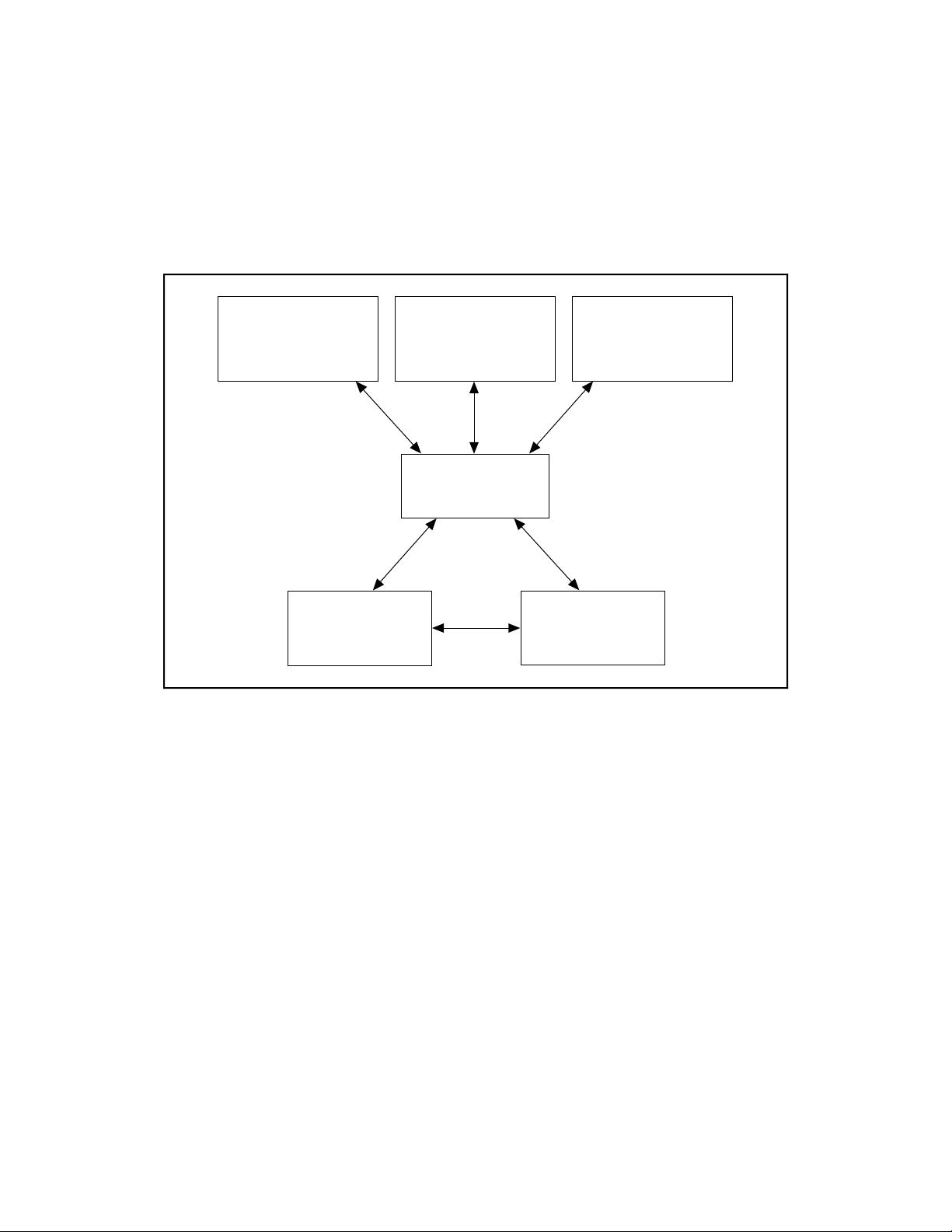
as illustrated in Figure 1-1.
Conventional
Programming Environment
(PC, Macintosh, or
Sun SPARCstation)
DAQ or
SCXI Hardware
LabVIEW
(PC, Macintosh, or
Sun SPARCstation)
NI-DAQ
Driver Software
LabWindows/CVI
(PC or Sun
SPARCstation)
Personal
Computer or
Workstation
Figure 1-1. The Relationship between the Programming Environment, NI-DAQ,
and Your Hardware
You can use your Lab-PC+ board, together with other PC, AT, EISA, DAQCard, and DAQPad
Series DAQ and SCXI hardware, with NI-DAQ software for PC compatibles.
Register-Level Programming
The final option for programming any National Instruments DAQ hardware is to write registerlevel software. Writing register-level programming software can be very time-consuming and
inefficient and is not recommended for most users.
Even if you are an experienced register-level programmer, consider using NI-DAQ, LabVIEW,
or LabWindows/CVI to program your National Instruments DAQ hardware. Using the NI-DAQ,
LabVIEW, or LabWindows/CVI software is as easy and as flexible as register-level
programming and can save weeks of development time.
© National Instruments Corporation 1-3 Lab-PC+ User Manual
Page 16

Introduction Chapter 1
Optional Equipment
National Instruments offers a variety of products to use with your Lab-PC+ board, including
cables, connector blocks, and other accessories, as follows:
• Cables and cable assemblies, shielded and ribbon
• Connector blocks, shielded and unshielded 50, 68, and 100-pin screw terminals
• Real Time System Integration (RTSI) bus cables
• Signal Condition eXtension for Instrumentation (SCXI) modules and accessories for
isolating, amplifying, exciting, and multiplexing signals for relays and analog output. With
SCXI you can condition and acquire up to 3072 channels.
• Low channel count signal conditioning modules, boards, and accessories, including
conditioning for strain gauges and RTDs, simultaneous sample and hold, and relays
For more specific information about these products, refer to your National Instruments catalogue
or call the office nearest you.
Unpacking
Your Lab-PC+ board is shipped in an antistatic package to prevent electrostatic damage to the
board. Electrostatic discharge can damage several components on the board. To avoid such
damage in handling the board, take the following precautions:
• Ground yourself via a grounding strap or by holding a grounded object.
• Touch the antistatic package to a metal part of your computer chassis before removing the
board from the package.
• Remove the board from the package and inspect the board for loose components or any other
sign of damage. Notify National Instruments if the board appears damaged in any way. Do
not install a damaged board into your computer.
Lab-PC+ User Manual 1-4 © National Instruments Corporation
Page 17

Chapter 2 Configuration and Installation
This chapter describes the Lab-PC+ jumper configuration and installation of the Lab-PC+ board
in your computer.
Board Configuration
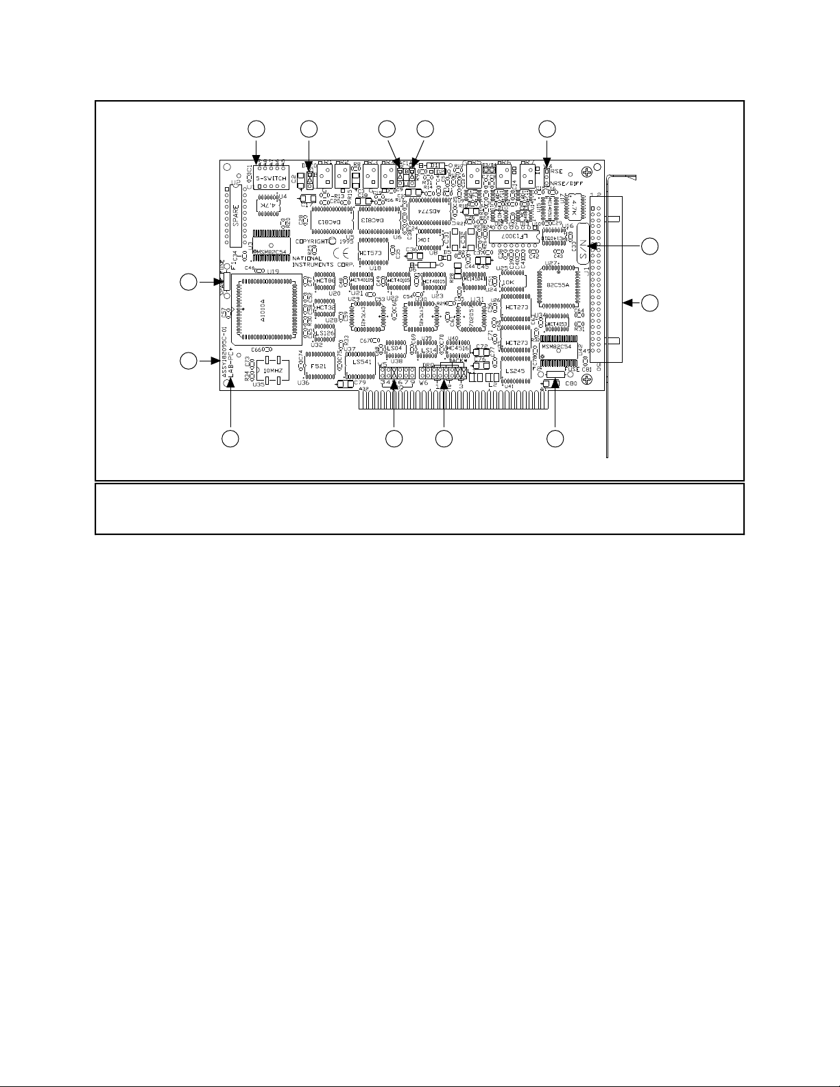
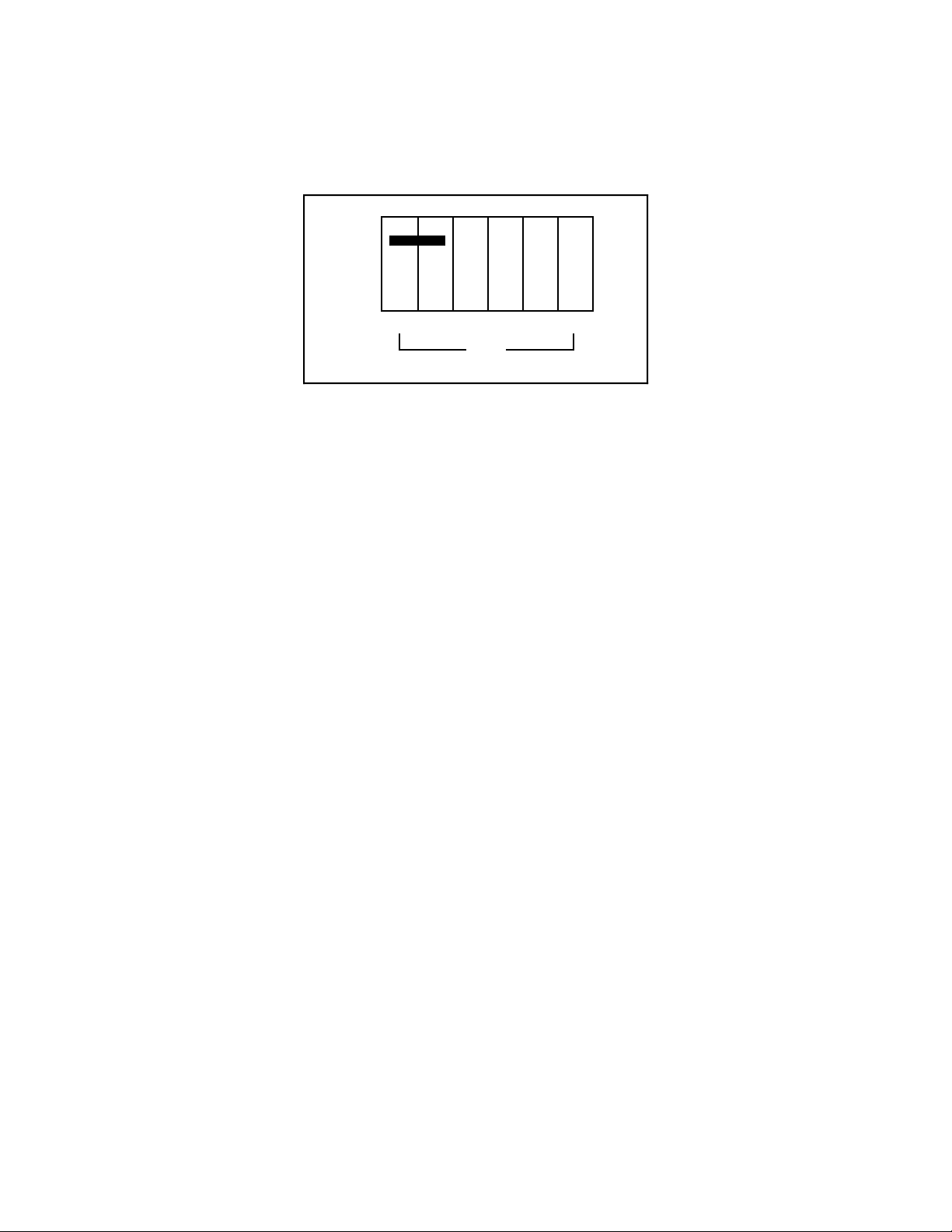
The Lab-PC+ contains six jumpers and one DIP switch to configure the PC bus interface and
analog I/O settings. The DIP switch is used to set the base I/O address. Two jumpers are used as
interrupt channel and DMA selectors. The remaining four jumpers are used to change the analog
input and analog output circuitry. The parts locator diagram in Figure 2-1 shows the Lab-PC+
jumper settings. Jumpers W3 and W4 configure the analog input circuitry. Jumpers W1 and W2
configure the analog output circuitry. Jumpers W6 and W5 select the DMA channel and the
interrupt level, respectively.
PC Bus Interface
The Lab-PC+ is configured at the factory to a base I/O address of hex 260, to use DMA
Channel 3, and to use interrupt level 5. These settings (shown in Table 2-1) are suitable for most
systems. If your system, however, has other hardware at this base I/O address, DMA channel, or
interrupt level, you will need to change these settings on the other hardware or on the Lab-PC+
as described in the following pages. Record your settings in the Lab-PC+ Hardware and
Software Configuration Form in Appendix F.
© National Instruments Corporation 2-1 Lab-PC+ User Manual
Page 18
Configuration and Installation Chapter 2
3 4 7
2
1
13 12 11 10
5 6
8
9
1 Assembly Number 5 W2 8 Serial Number 11 W6
2 Spare Fuse 6 W3 9 J1 12 W5
3 U1 7 W4 10 Fuse 13 Product Name
4W1
Figure 2-1. Parts Locator Diagram
Lab-PC+ User Manual 2-2 © National Instruments Corporation
Page 19
Chapter 2 Configuration and Installation
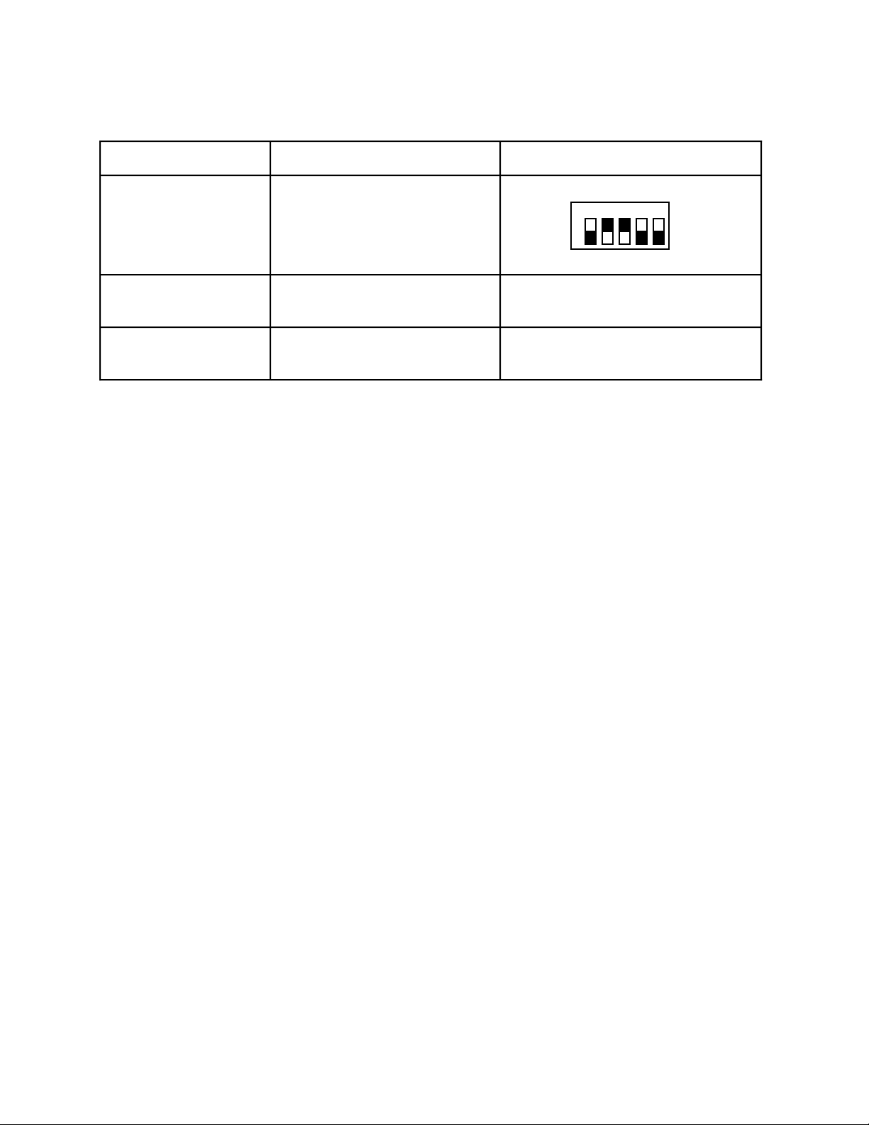
Table 2-1. PC Bus Interface Factory Settings
Lab-PC+ Board Default Settings Hardware Implementation
Base I/O Address Hex 260
DMA Channel DMA Channel 3
A9A8A7
1 2 3 4 5
O
N
O
F
F
W6: DRQ3, DACK*3
A6
A5
U1
(factory setting)
Interrupt Level Interrupt level 5 selected
W5: Row 5
(factory setting)
Note: The shaded portion indicates the side of the switch that is pressed down.
Base I/O Address Selection
The base I/O address for the Lab-PC+ is determined by the switches at position U1 (see
Figure 2-1). The switches are set at the factory for the base I/O address hex 260. This factory
setting is used as the default base I/O address value by National Instruments software packages
for use with the Lab-PC+. The Lab-PC+ uses the base I/O address space hex 260 through 27F
with the factory setting.
Note: Verify that this space is not already used by other equipment installed in your
computer. If any equipment in your computer uses this base I/O address space, you
must change the base I/O address of the Lab-PC+ or of the other device. If you change
the Lab-PC+ base I/O address, you must make a corresponding change to any software
packages you use with the Lab-PC+. For more information about your computer’s
I/O, refer to your computer’s technical reference manual.
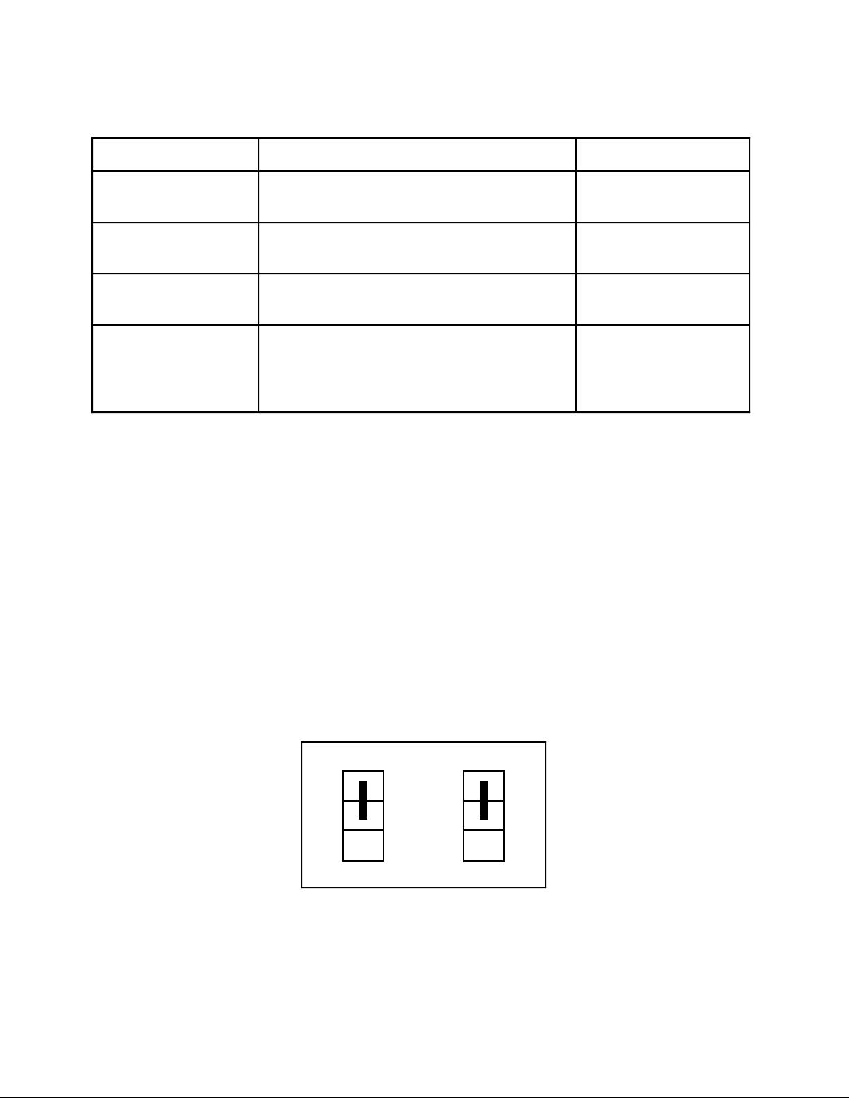
Each switch in U1 corresponds to one of the address lines A9 through A5. Press the side marked
OFF to select a binary value of 1 for the corresponding address bit. Press the other side of the
switch to select a binary value of 0 for the corresponding address bit. Figure 2-2 shows two
possible switch settings.
© National Instruments Corporation 2-3 Lab-PC+ User Manual
Page 20
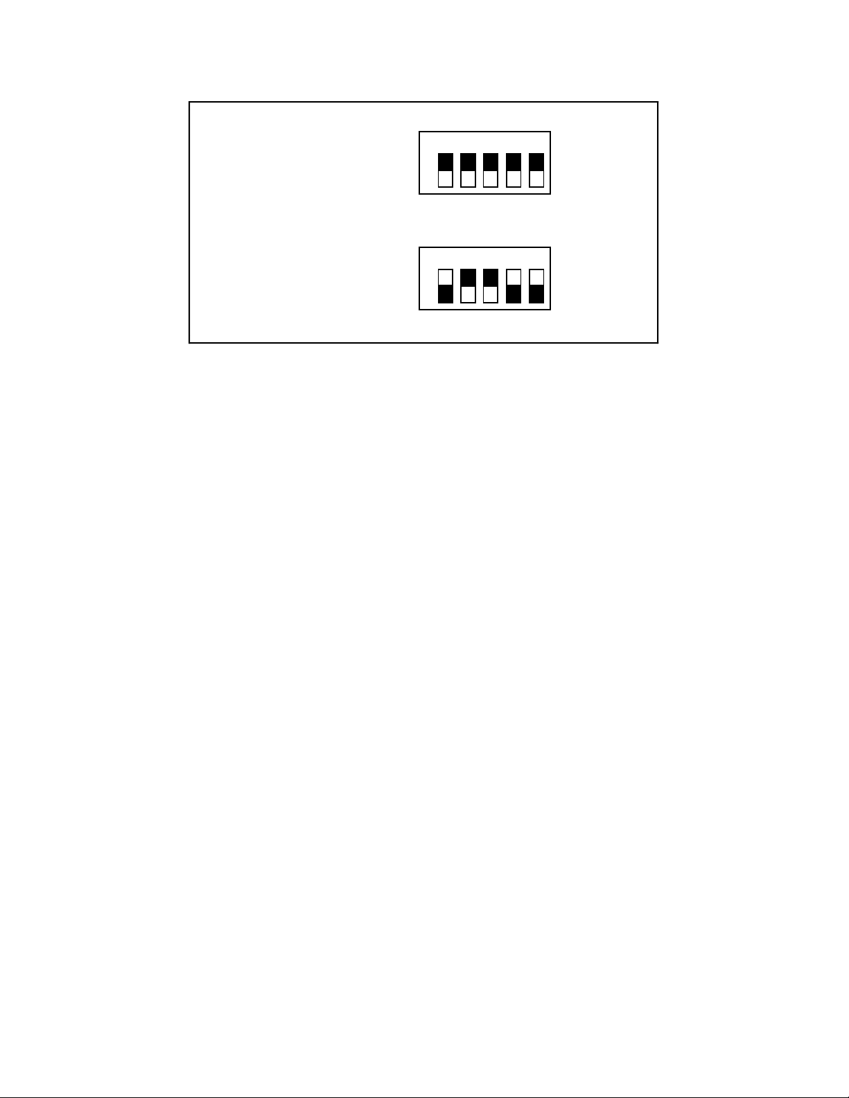
Configuration and Installation Chapter 2
A9
A8
A7
A6
A5
1 2 3 4 5
This side down for 0 —
This side down for 1 —
O
N
O
F
F
U1
A. Switches Set to Base I/O Address of Hex 000
A9
A8
A7
A6
A5
1 2 3 4 5
This side down for 0 —
This side down for 1 —
O
N
O
F
F
U1
B. Switches Set to Base I/O Address of Hex 260 (Factory Setting)
Figure 2-2. Example Base I/O Address Switch Settings
The five least significant bits of the address (A4 through A0) are decoded by the Lab-PC+ to
select the appropriate Lab-PC+ register. To change the base I/O address, remove the plastic
cover on U1; press each switch to the desired position; check each switch to make sure the
switch is pressed down all the way; and replace the plastic cover. Record the new Lab-PC+ base
I/O address in Appendix F, Customer Communication, for use when configuring the Lab-PC+
software.
Table 2-2 lists the possible switch settings, the corresponding base I/O address, and the base I/O
address space used for that setting.
Lab-PC+ User Manual 2-4 © National Instruments Corporation
Page 21

Chapter 2 Configuration and Installation
Table 2-2. Switch Settings with Corresponding Base I/O Address
and Base I/O Address Space
Switch Setting
A9 A8 A7 A6 A5
Base I/O Address
(hex)
Base I/O Address
Space Used (hex)
0 0 0 0 0 000 000 - 01F
0 0 0 0 1 020 020 - 03F
0 0 0 1 0 040 040 - 05F
0 0 0 1 1 060 060 - 07F
0 0 1 0 0 080 080 - 09F
0 0 1 0 1 0A0 0A0 - 0BF
0 0 1 1 0 0C0 0C0 - 0DF
0 0 1 1 1 0E0 0E0 - 0FF
0 1 0 0 0 100 100 - 11F
0 1 0 0 1 120 120 - 13F
0 1 0 1 0 140 140 - 15F
0 1 0 1 1 160 160 - 17F
0 1 1 0 0 180 180 - 19F
0 1 1 0 1 1A0 1A0 - 1BF
0 1 1 1 0 1C0 1C0 - 1DF
0 1 1 1 1 1E0 1E0 - 1FF
1 0 0 0 0 200 200 - 21F
1 0 0 0 1 220 220 - 23F
1 0 0 1 0 240 240 - 25F
1 0 0 1 1 260 260 - 27F
1 0 1 0 0 280 280 - 29F
1 0 1 0 1 2A0 2A0 - 2BF
1 0 1 1 0 2C0 2C0 - 2DF
1 0 1 1 1 2E0 2E0 - 2FF
1 1 0 0 0 300 300 - 31F
1 1 0 0 1 320 320 - 33F
1 1 0 1 0 340 340 - 35F
1 1 0 1 1 360 360 - 37F
1 1 1 0 0 380 380 - 39F
1 1 1 0 1 3A0 3A0 - 3BF
1 1 1 1 0 3C0 3C0 - 3DF
1 1 1 1 1 3E0 3E0 - 3FF
Note:Base I/O address values hex 000 through 0FF are reserved for system use.
Base I/O address values hex 100 through 3FF are available on the I/O channel.
© National Instruments Corporation 2-5 Lab-PC+ User Manual
Page 22

Configuration and Installation Chapter 2
DMA Channel Selection
The Lab-PC+ uses the DMA channel selected by jumpers on W6 (see Figure 2-1). The Lab-PC+
is set at the factory to use DMA Channel 3. This is the default DMA channel used by the
Lab-PC+ software handler. Verify that other equipment already installed in your computer does
not use this DMA channel. If any device uses DMA Channel 3, change the DMA channel used
by either the Lab-PC+ or the other device. The Lab-PC+ hardware can use DMA Channels 1, 2,
and 3. Notice that these are the three 8-bit channels on the PC I/O channel. The Lab-PC+ does
not use and cannot be configured to use the 16-bit DMA channels on the PC AT I/O channel.
Each DMA channel consists of two signal lines as shown in Table 2-3.
Table 2-3. DMA Channels for the Lab-PC+
DMA
Channel
DMA
Acknowledge
DMA
Request
1 DACK1 DRQ1
2 DACK2 DRQ2
3 DACK3 DRQ3
Note: In most personal computers DMA Channel 2 is
reserved for the disk drives. Therefore, you should
avoid using this channel.
Two jumpers must be installed to select a DMA channel. The DMA Acknowledge and DMA
Request lines selected must have the same number suffix for proper operation. Figure 2-3
displays the jumper positions for selecting DMA Channel 3.
DACK*
DRQ
•••••••••••••••
W6
•
12
3
Figure 2-3. DMA Jumper Settings for DMA Channel 3 (Factory Setting)
If you do not want to use DMA for Lab-PC+ transfers, then place the configuration jumpers on
W6 in the position shown in Figure 2-4.
Lab-PC+ User Manual 2-6 © National Instruments Corporation
Page 23

Chapter 2 Configuration and Installation
DACK*
DRQ
•••••••••••••••
W6
•
12
3
Figure 2-4. DMA Jumper Settings for Disabling DMA Transfers
Interrupt Selection
The Lab-PC+ board can connect to any one of the six interrupt lines of the PC I/O channel. The
interrupt line is selected by a jumper on one of the double rows of pins located above the I/O slot
edge connector on the Lab-PC+ (refer to Figure 2-1). To use the interrupt capability of the
Lab-PC+, you must select an interrupt line and place the jumper in the appropriate position to
enable that particular interrupt line.
The Lab-PC+ can share interrupt lines with other devices by using a tristate driver to drive its
selected interrupt line. The Lab-PC+ hardware supports interrupt lines IRQ3, IRQ4, IRQ5,
IRQ6, IRQ7, and IRQ9.
Note: Do not use interrupt line 6. Interrupt line 6 is used by the diskette drive controller on
most IBM PC and compatible computers.
Once you have selected an interrupt level, place the interrupt jumper on the appropriate pins to
enable the interrupt line.
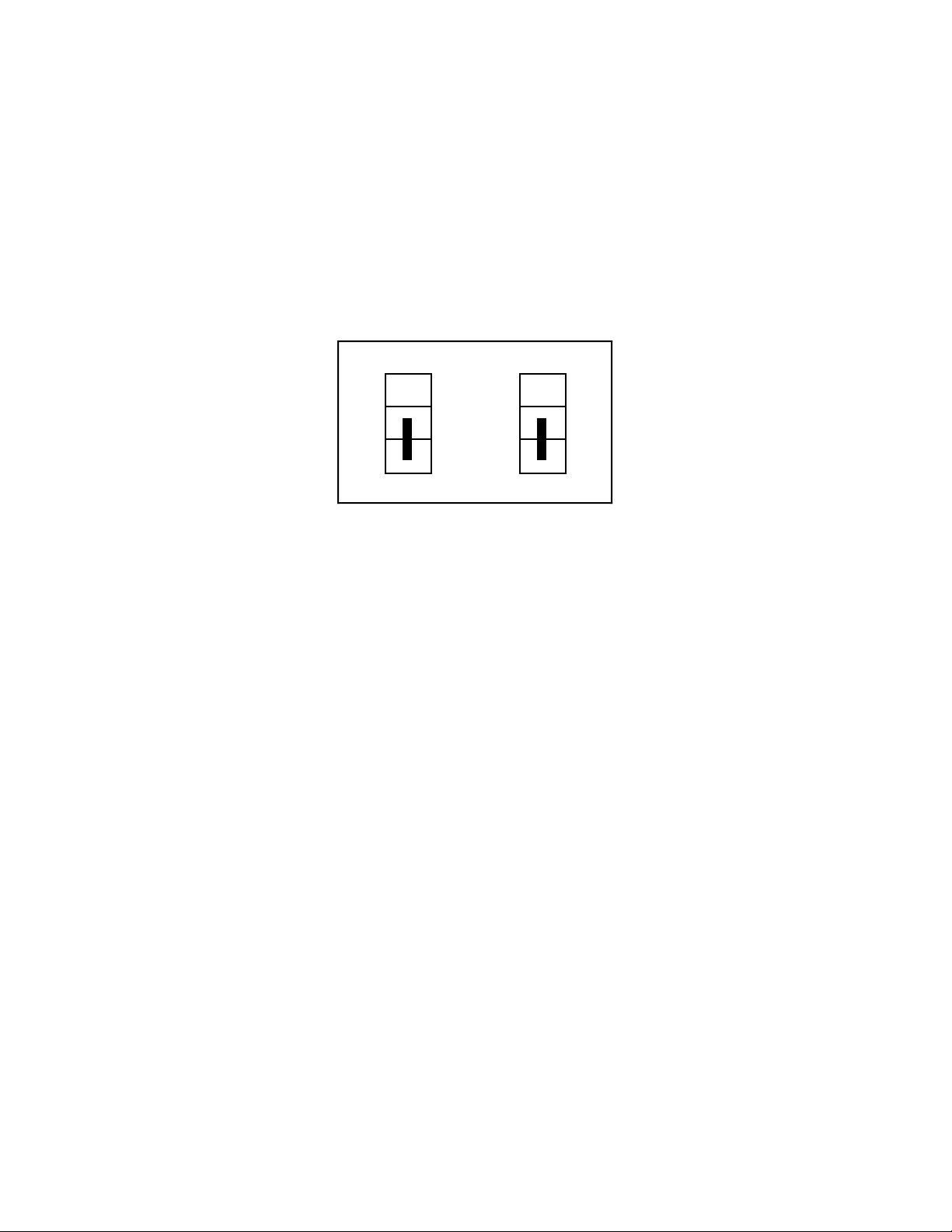
The interrupt jumper set is W5. The default interrupt line is IRQ5, which you select by placing
the jumper on the pins in row 5. Figure 2-5 shows the default interrupt jumper setting IRQ5. To
change to another line, remove the jumper from IRQ5 and place it on the new pins.
•••••••••••
W5
•
3 4 5 6 7 9
IRQ
Figure 2-5. Interrupt Jumper Setting IRQ5 (Factory Setting)
© National Instruments Corporation 2-7 Lab-PC+ User Manual
Page 24
Configuration and Installation Chapter 2
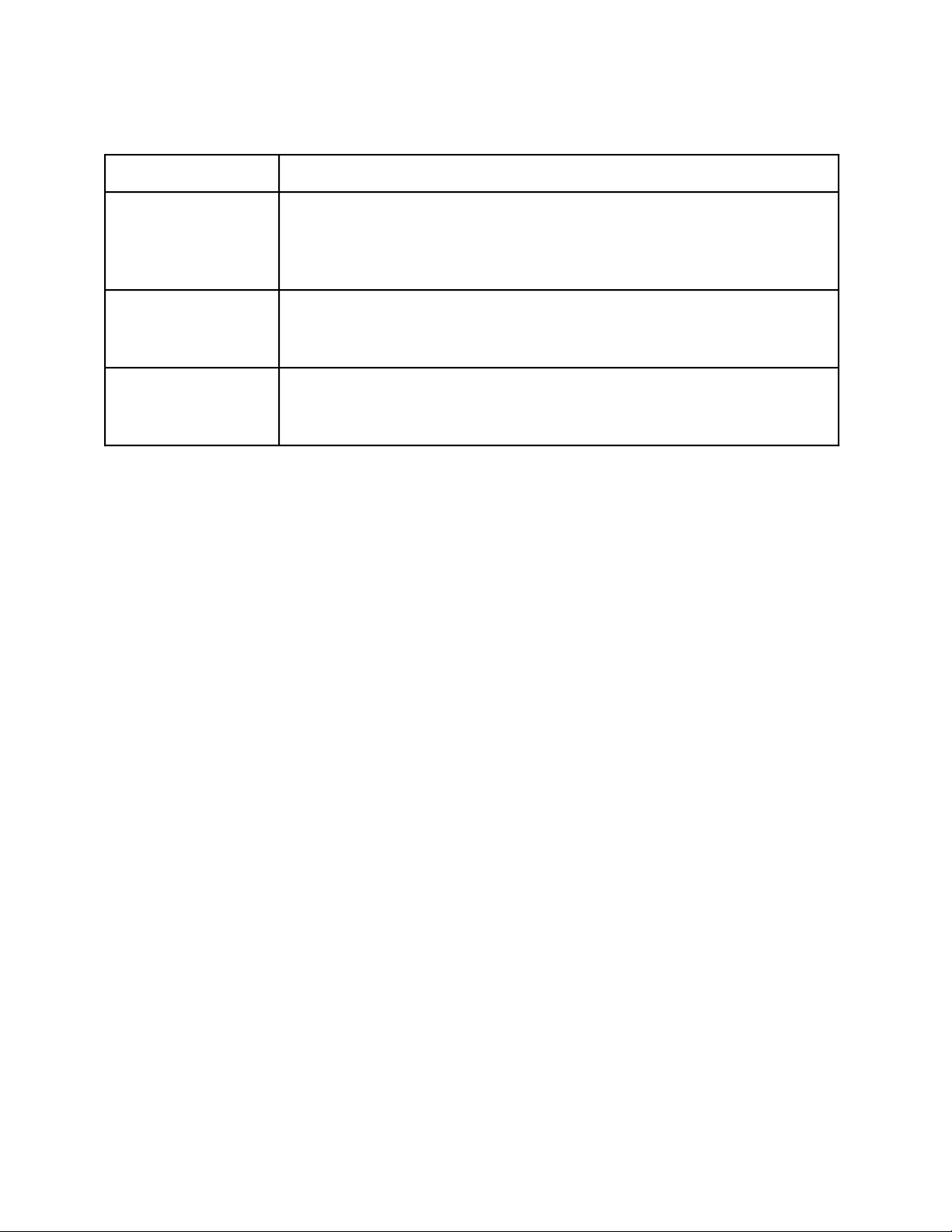
If you do not want to use interrupts, place the jumper on W5 in the position shown in Figure 2-6.
This setting disables the Lab-PC+ from asserting an interrupt line on the PC I/O channel.
•••••••••••
W5
•
3 4 5 6 7 9
IRQ
Figure 2-6. Interrupt Jumper Setting for Disabling Interrupts
Analog I/O Configuration
The Lab-PC+ is shipped from the factory with the following configuration:
• Referenced single-ended input mode
• ±5 V input range
• Bipolar analog output
• ±5 V output range
Table 2-4 lists all the available analog I/O jumper configurations for the Lab-PC+ with the
factory settings noted.
Lab-PC+ User Manual 2-8 © National Instruments Corporation
Page 25
Chapter 2 Configuration and Installation
Table 2-4. Analog I/O Jumper Settings
Parameter Configuration Jumper Settings
Output CH0 Polarity Bipolar: ±5 V (factory setting)
Unipolar: 0 to 10 V
Output CH1 Polarity Bipolar: ±5 V (factory setting)
Unipolar: 0 to 10 V
Input Range Bipolar: ±5 V (factory setting)
Unipolar: 0 to 10 V
Input Mode Referenced single-ended (RSE)
W1: A-B
W1: B-C
W2: A-B
W2: B-C
W3: A-B
W3: B-C
W4: A-B
(factory setting)
Nonreferenced single-ended (NRSE)
Differential (DIFF)
W4: B-C
W4: B-C
Analog Output Configuration
Two ranges are available for the analog outputs–bipolar: ±5 V and unipolar: 0 to 10 V. Jumper
W1 controls output Channel 0, and W2 controls output Channel 1.
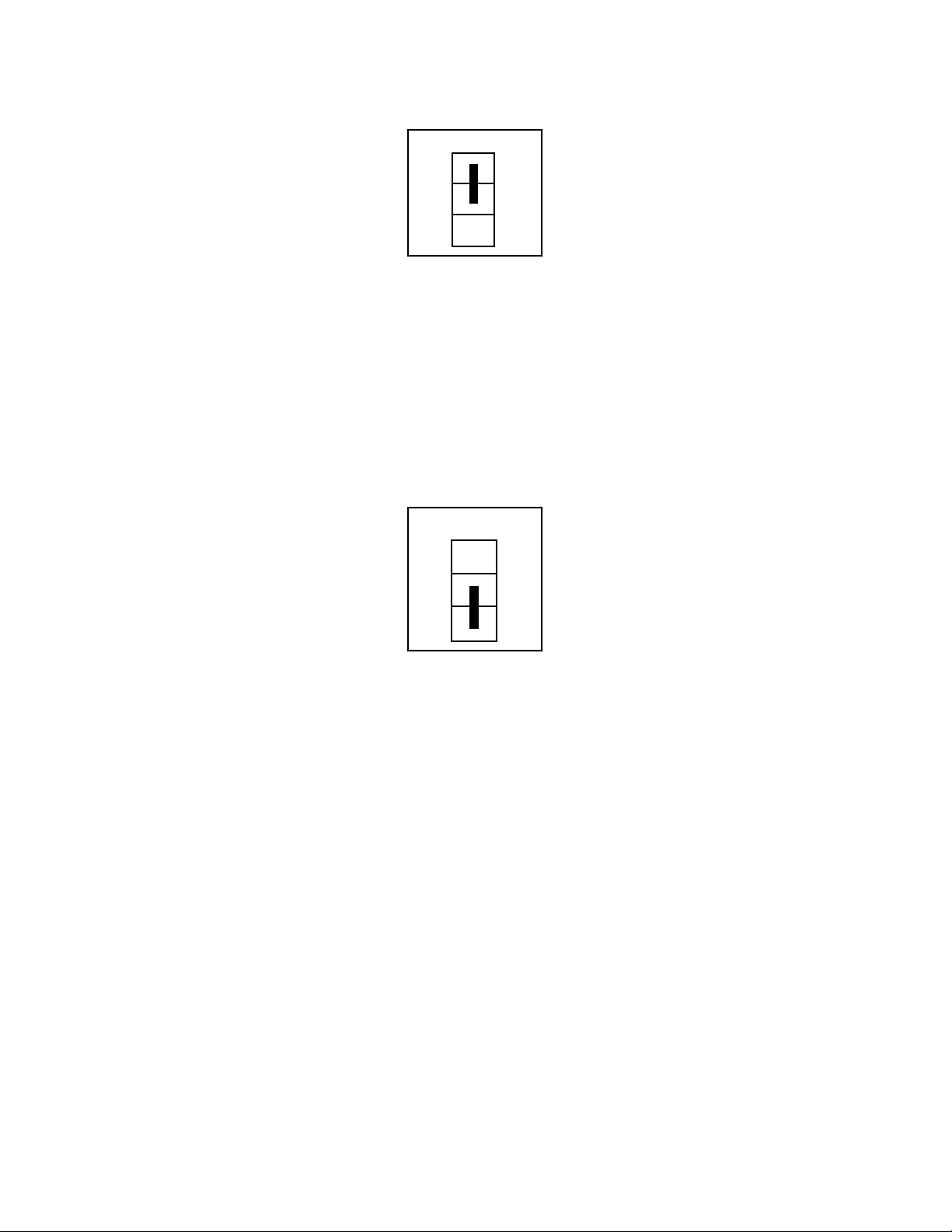
Bipolar Output Selection
You can select the bipolar (±5 V) output configuration for either analog output channel by setting
the following jumpers:
Analog Output Channel 0 W1 A-B
Analog Output Channel 1 W2 A-B
This configuration is shown in Figure 2-7.
W1
•
A
B
•
B
•
C
Channel 0
Figure 2-7. Bipolar Output Jumper Configuration (Factory Setting)
U
W2
•
A
•
B
•
C
Channel 1
B
U
© National Instruments Corporation 2-9 Lab-PC+ User Manual
Page 26
Configuration and Installation Chapter 2
Unipolar Output Selection
You can select the unipolar (0 V to 10 V) output configuration for either analog output channel
by setting the following jumpers:
Analog Output Channel 0 W1 B-C
Analog Output Channel 1 W2 B-C
This configuration is shown in Figure 2-8.
A
B
C
Channel 0
W1
•
B
•
•
U
A
B
C
Channel 1
W2
•
B
•
•
U
Figure 2-8. Unipolar Output Jumper Configuration
Analog Input Configuration
You can select different analog input configurations by using the jumper and register bit
(software) settings as shown in Table 2-4. The following sections describe each of the analog
input categories in detail.
Input Mode
The Lab-PC+ features three different input modes–referenced single-ended (RSE) input, nonreferenced single-ended (NRSE) input, and differential (DIFF) input. The single-ended input
configurations use eight channels. The DIFF input configuration uses four channels. These
configurations are described in Table 2-5.
Lab-PC+ User Manual 2-10 © National Instruments Corporation
Page 27
Chapter 2 Configuration and Installation
Table 2-5. Input Configurations Available for the Lab-PC+
Configuration Description
DIFF Differential configuration provides four differential inputs with the
positive (+) input of the instrumentation amplifier tied to Channels 0,
2, 4, or 6 and the negative (-) input tied to Channels 1, 3, 5, or 7
respectively, thus choosing channel pairs (0,1), (2,3), (4,5), or (6,7).
NRSE Non-referenced single-ended configuration provides eight single-ended
inputs with the negative input of the instrumentation amplifier tied to
AISENSE/AIGND and not connected to ground.
RSE Referenced single-ended configuration provides eight single-ended
inputs with the negative input of the instrumentation amplifier
referenced to analog ground.
While reading the following paragraphs, you may find it helpful to refer to Analog Input Signal
Connections in Chapter 3, Signal Connections, which contains diagrams showing the signal
paths for the three configurations.
DIFF Input (Four Channels)
DIFF input means that each input signal has its own reference, and the difference between each
signal and its reference is measured. The signal and its reference are each assigned an input
channel. With this input configuration, the Lab-PC+ can monitor four differential analog input
signals. To select the DIFF mode, you must set the SE__/D bit as described in the Command
Register 4 bit description in Appendix D, Register Map and Descriptions. You must also set the
following jumper.
W4: B-C Jumper is in stand-by position, and negative input of instrumentation amplifier
is tied to multiplexer output.
© National Instruments Corporation 2-11 Lab-PC+ User Manual
Page 28
Configuration and Installation Chapter 2
This configuration is shown in Figure 2-9.
W4
A
B
C
•
RSE
NRSE/DIFF
Figure 2-9. DIFF Input Configuration
Considerations in using the DIFF configuration are discussed in Chapter 3, Signal Connections.
Note that the signal return path is through the negative terminal of the amplifier and through
Channels 1, 3, 5, or 7, depending on which channel pair was selected.
RSE Input (Eight Channels, Factory Setting)
RSE input means that all input signals are referenced to a common ground point that is also tied
to the analog input ground of the Lab-PC+. The negative input of the differential amplifier is
tied to analog ground. This configuration is useful when measuring floating signal sources.
See Types of Signal Sources in Chapter 3, Signal Connections. With this input configuration, the
Lab-PC+ can monitor eight different analog input channels. To select the RSE input
configuration, clear the SE__/D bit as described in the Command Register 4 bit description in
Appendix D, Register Map and Descriptions. You must also set the following jumper.
W4: A-B Jumper connects the negative input of the instrumentation amplifier to analog
ground.
This configuration is shown in Figure 2-10.
W4
A
B
C
RSE
NRSE/DIFF
•
Figure 2-10. RSE Input Configuration
Considerations in using the RSE configuration are discussed in Chapter 3, Signal Connections.
Note that in this mode, the return path of the signal is analog ground, available at the connector
through pin AISENSE/AIGND.
Lab-PC+ User Manual 2-12 © National Instruments Corporation
Page 29
Chapter 2 Configuration and Installation
NRSE Input (Eight Channels)
NRSE input means that all input signals are referenced to the same common mode voltage,
which is allowed to float with respect to the analog ground of the Lab-PC+ board. This common
mode voltage is subsequently subtracted out by the input instrumentation amplifier. This
configuration is useful when measuring ground-referenced signal sources. To select the NRSE
input configuration, clear the SE__/D bit as described in the Command Register 4 bit description in
Appendix D, Register Map and Descriptions. You must also set the following jumper.
W4: B-C Jumper is in standby position, and negative input of instrumentation amplifier
is tied to multiplexed output.
This configuration is shown in Figure 2-11.
W4
A
B
C
•
RSE
NRSE/DIFF
Figure 2-11. NRSE Input Configuration
Considerations in using the NRSE configuration are discussed in Chapter 3, Signal Connections.
Note that in this mode, the return path of the signal is through the negative terminal of the
amplifier, available at the connector through the pin AISENSE/AIGND.
Analog Input Polarity Configuration
Two ranges are available for the analog inputs–bipolar ±5 V and unipolar 0 to 10 V. Jumper W3
controls the input range for all eight analog input channels.
Bipolar Input Selection
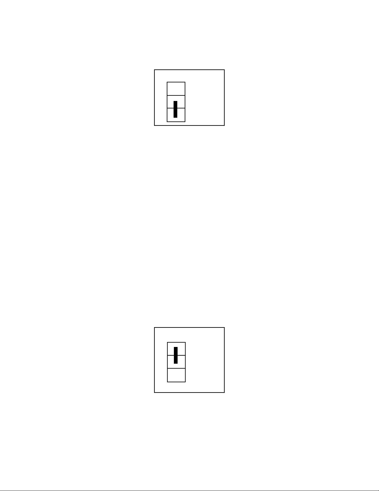
You can select the bipolar (±5 V) input configuration by setting the following jumper:
Analog Input W3 A-B
This configuration is shown in Figure 2-12.
© National Instruments Corporation 2-13 Lab-PC+ User Manual
Page 30
Configuration and Installation Chapter 2
W3
•
B
A
•
B
•
U
Figure 2-12. Bipolar Input Jumper Configuration (Factory Setting)
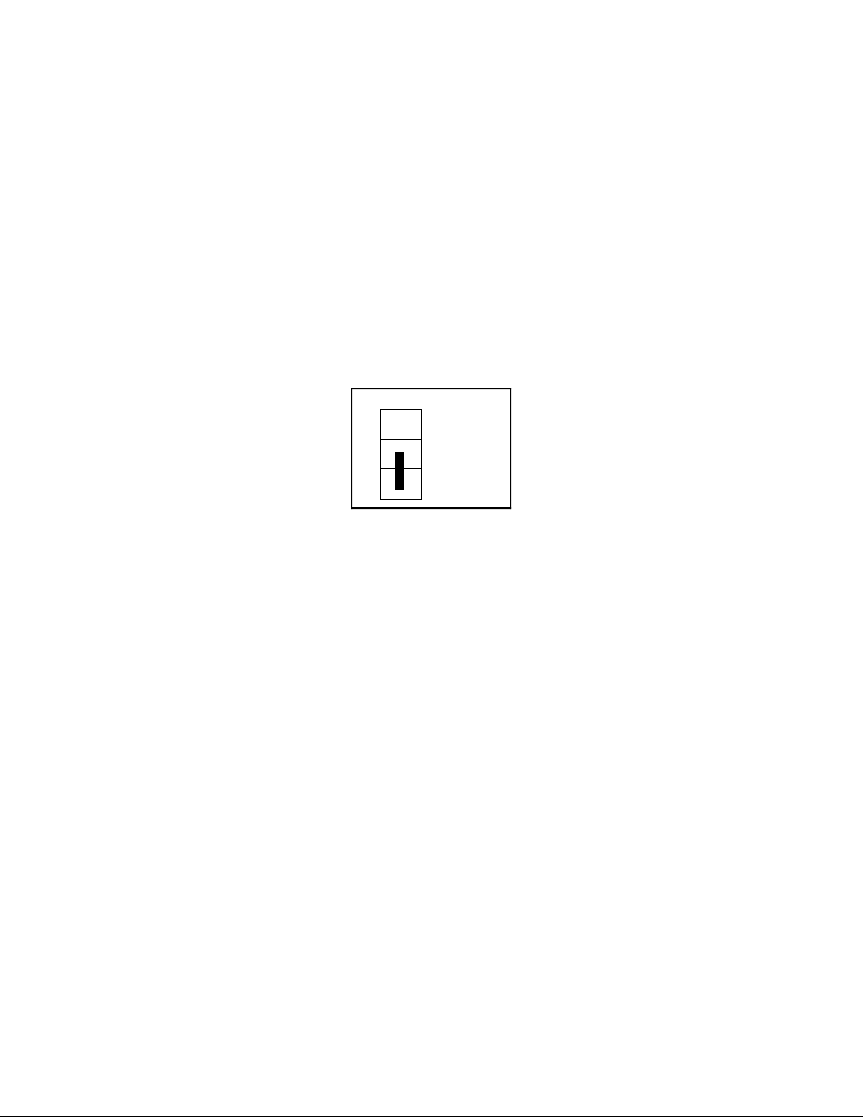
Unipolar Input Selection
You can select the unipolar (0 to 10 V) input configuration by setting the following jumper:
Analog Input W3 B-C
This configuration is shown in Figure 2-13.
C
W3
•
B
A
•
B
•
U
Figure 2-13. Unipolar Input Jumper Configuration
Note: If you are using a software package such as NI-DAQ or LabWindows/CVI, you may
need to reconfigure your software to reflect any changes in jumper or switch settings.
C
Lab-PC+ User Manual 2-14 © National Instruments Corporation
Page 31

Chapter 2 Configuration and Installation
Hardware Installation
The Lab-PC+ can be installed in any available 8-bit or 16-bit expansion slot in your computer.
After you have changed (if necessary), verified, and recorded the switches and jumper settings,
you are ready to install the Lab-PC+. The following are general installation instructions, but
consult your PC user manual or technical reference manual for specific instructions and
warnings.
1. Turn off your computer.
2. Remove the top cover or access port to the I/O channel.
3. Remove the expansion slot cover on the back panel of the computer.
4. Insert the Lab-PC+ into an 8-bit or a 16-bit slot.
5. Screw the mounting bracket of the Lab-PC+ to the back panel rail of the computer.
6. Check the installation.
7. Replace the cover.
The Lab-PC+ board is installed. You are now ready to install and configure your software.
If you are using NI-DAQ, refer to your NI-DAQ release notes. Find the installation and system
configuration section for your operating system and follow the instructions given there.
If you are using LabVIEW, the software installation instructions are in your LabVIEW release
notes.
If you are using LabWindows/CVI, the software installation instructions are in your
LabWindows/CVI release notes.
If you are a register-level programmer, refer to Appendix E, Register-Level Programming.
© National Instruments Corporation 2-15 Lab-PC+ User Manual
Page 32

Chapter 3 Signal Connections
This chapter describes how to make input and output signal connections to your Lab-PC+ board
via the board I/O connector.
I/O Connector Pin Description
Figure 3-1 shows the pin assignments for the Lab-PC+ I/O connector. This connector is located
on the back panel of the Lab-PC+ board and is accessible at the rear of the PC after the board has
been properly installed.
Warning: Connections that exceed any of the maximum ratings of input or output signals
on the Lab-PC+ may result in damage to the Lab-PC+ board and to the computer.
This includes connecting any power signals to ground and vice versa. National
Instruments is
connections.
NOT liable for any damages resulting from any such signal
© National Instruments Corporation 3-1 Lab-PC+ User Manual
Page 33

Signal Connections Chapter 3
ACH0
ACH2
ACH4
ACH6
AISENSE/AIGND
PC3
12
34
56
78
9 10
11 12
13 14
15 16
17 18
19 20
21 22
23 24
25
26
27 28
29 30
31 32
33 34
ACH1
ACH3
ACH5
ACH7
DAC0 OUT
DAC1 OUTAGND
PA 0DGND
PA 2PA 1
PA 4PA 3
PA 6PA 5
PB0PA7
PB2PB1
PB4PB3
PB6PB5
PC0PB7
PC2PC1
PC4
PC5 PC6
35 36
PC7 EXTTRIG
37 38
EXTUPDATE*
OUTB0
CCLKB1
+5 V
39 40
41 42
43 44
45 46
47 48
49 50
EXTCONV*
GATB0
GATB1COUTB1
OUTB2
CLKB2GATB2
DGND
Figure 3-1. Lab-PC+ I/O Connector Pin Assignments
Signal Connection Descriptions
The following list describes the connector pins on the Lab-PC+ I/O connector by pin number and
gives the signal name and the significance of each signal connector pin.
Lab-PC+ User Manual 3-2 © National Instruments Corporation
Page 34

Chapter 3 Signal Connections
Pin Signal Name Description
1-8 ACH0 through ACH7 Analog input Channels 0 through 7 (single-ended).
9 AISENSE/AIGND Analog input ground in RSE mode, AISENSE in NRSE
mode. Bi-directional.
10 DAC0 OUT Voltage output signal for analog output Channel 0.
11 AGND Analog ground. Analog output ground for analog
output mode. Analog input ground for DIFF or NRSE
mode. Bi-directional.
12 DAC1 OUT Voltage output signal for analog output Channel 1.
13 DGND Digital ground. Output.
14-21 PA0 through PA7 Bidirectional data lines for Port A. PA7 is the MSB,
PA0 the LSB.
22-29 PB0 through PB7 Bidirectional data lines for Port B.
PB7 is the MSB, PB0 the LSB.
30-37 PC0 through PC7 Bidirectional data lines for Port C.
PC7 is the MSB, PC0 the LSB.
38 EXTTRIG External control signal to start a timed conversion
sequence. Input.
39 EXTUPDATE* External control signal to update DAC outputs. Input.
40 EXTCONV* External control signal to trigger A/D conversions.
Bi-directional.
41 OUTB0 Counter B0 output.
42 GATB0 Counter B0 gate. Input.
43 COUTB1 Counter B1 output or pulled high (selectable).
44 GATB1 Counter B1 gate. Input.
45 CCLKB1 Counter B1 clock (selectable). Input.
46 OUTB2 Counter B2 output.
47 GATB2 Counter B2 gate. Input.
48 CLKB2 Counter B2 clock. Input.
49 +5V +5 V out, 1 A maximum. Output.
50 DGND Digital ground. Output.
*Indicates that the signal is active low.
© National Instruments Corporation 3-3 Lab-PC+ User Manual
Page 35

Signal Connections Chapter 3
The connector pins can be grouped into analog input signal pins, analog output signal pins,
digital I/O signal pins, and timing I/O signal pins. Signal connection guidelines for each of these
groups are included later in this chapter.
Analog Input Signal Connections
Pins 1 through 8 are analog input signal pins for the 12-bit ADC. Pin 9, AISENSE/AIGND, is
an analog common signal. This pin can be used for a general analog power ground tie to the
Lab-PC+ in RSE mode, or as a return path in DIFF or NRSE mode. Pins 1 through 8 are tied to
the eight single-ended analog input channels of the input multiplexer through 4.7 kΩ series
resistances. Pins 2, 4, 6, and 8 are also tied to an input multiplexer for DIFF mode. Pin 40 is
EXTCONV* and can be used to trigger conversions. A conversion occurs when this signal
makes a high-to-low transition.
The following input ranges and maximum ratings apply to inputs ACH<0..7>:
Input signal range Bipolar input: ±(5/gain) V
Unipolar input: 0 to (10/gain) V
Maximum input voltage rating ±45 V powered on or off
Exceeding the input signal range for gain settings greater than 1 will not damage the input
circuitry as long as the maximum input voltage rating of ±45 V is not exceeded. For example
with a gain of 10, the input signal range is ±0.5 V for bipolar input and 0 to 1V for unipolar
input, but the Lab-PC+ is guaranteed to withstand inputs up to the maximum input voltage rating.
Warning: Exceeding the input signal range results in distorted input signals. Exceeding the
maximum input voltage rating may cause damage to the Lab-PC+ board and to
the computer. National Instruments is
NOT liable for any damages resulting from
such signal connections.
Connection of analog input signals to the Lab-PC+ depends on the configuration of the Lab-PC+
analog input circuitry and the type of input signal source. With the different Lab-PC+
configurations, the Lab-PC+ instrumentation amplifier can be used in different ways. Figure 3-2
shows a diagram of the Lab-PC+ instrumentation amplifier.
Lab-PC+ User Manual 3-4 © National Instruments Corporation
Page 36

Chapter 3 Signal Connections
Instrumentation
Vin+
Vin-
+
-
Vm = [Vin+ - Vin-] * GAIN
Amplifier
V
m
+
Measured
Voltage
-
Figure 3-2. Lab-PC+ Instrumentation Amplifier
The Lab-PC+ instrumentation amplifier applies gain, common-mode voltage rejection, and highinput impedance to the analog input signals connected to the Lab-PC+ board. Signals are routed
to the positive and negative inputs of the instrumentation amplifier through input multiplexers on
the Lab-PC+. The instrumentation amplifier converts two input signals to a signal that is the
difference between the two input signals multiplied by the gain setting of the amplifier. The
amplifier output voltage is referenced to the Lab-PC+ ground. The Lab-PC+ ADC measures this
output voltage when it performs A/D conversions.
All signals must be referenced to ground, either at the source device or at the Lab-PC+. If you
have a floating source, you must use a ground-referenced input connection at the Lab-PC+. If
you have a grounded source, you must use a non-referenced input connection at the Lab-PC+.
Types of Signal Sources
When configuring the input mode of the Lab-PC+ and making signal connections, you should
first determine whether the signal source is floating or ground-referenced. These two types of
signals are described as follows.
Floating Signal Sources
A floating signal source is one that is not connected in any way to the building ground system
but rather has an isolated ground reference point. Some examples of floating signal sources are
outputs of transformers, thermocouples, battery-powered devices, optical isolator outputs, and
isolation amplifiers. The ground reference of a floating signal must be tied to the Lab-PC+
analog input ground in order to establish a local or onboard reference for the signal. Otherwise,
© National Instruments Corporation 3-5 Lab-PC+ User Manual
Page 37

Signal Connections Chapter 3
the measured input signal varies or appears to float. An instrument or device that provides an
isolated output falls into the floating signal source category.
Ground-Referenced Signal Sources
A ground-referenced signal source is one that is connected in some way to the building system
ground and is therefore already connected to a common ground point with respect to the
Lab-PC+, assuming that the PC is plugged into the same power system. Non-isolated outputs of
instruments and devices that plug into the building power system fall into this category.
The difference in ground potential between two instruments connected to the same building
power system is typically between 1 mV and 100 mV but can be much higher if power
distribution circuits are not properly connected. The connection instructions that follow for
grounded signal sources are designed to eliminate this ground potential difference from the
measured signal.
Input Configurations
The Lab-PC+ can be configured for one of three input modes–NRSE, RSE, or DIFF. The
following sections discuss the use of single-ended and differential measurements, and
considerations for measuring both floating and ground-referenced signal sources. Table 3-1
summarizes the recommended input configurations for both types of signal sources.
Table 3-1. Recommended Input Configurations for Ground-Referenced
and Floating Signal Sources
Type of Signal Recommended Input Configuration
Ground-Referenced
(non-isolated outputs,
plug-in instruments)
Floating
(batteries, thermocouples,
isolated outputs)
DIFF
NRSE
DIFF with bias resistors
RSE
Differential Connection Considerations (DIFF Configuration)
Differential connections are those in which each Lab-PC+ analog input signal has its own
reference signal or signal return path. These connections are available when the Lab-PC+ is
configured in the DIFF mode. Each input signal is tied to the positive input of the
instrumentation amplifier, and its reference signal, or return, is tied to the negative input of the
instrumentation amplifier.
Lab-PC+ User Manual 3-6 © National Instruments Corporation
Page 38

Chapter 3 Signal Connections
When the Lab-PC+ is configured for DIFF input, each signal uses two of the multiplexer inputs–
one for the signal and one for its reference signal. Therefore, only four analog input channels are
available when using the DIFF configuration. The DIFF input configuration should be used
when any of the following conditions are present:
• Input signals are low-level (less than 1 V).
• Leads connecting the signals to the Lab-PC+ are greater than 15 ft.
• Any of the input signals requires a separate ground reference point or return signal.
• The signal leads travel through noisy environments.
Differential signal connections reduce picked-up noise and increase common mode signal and
noise rejection. With these connections, input signals can float within the common mode limits
of the input instrumentation amplifier.
Differential Connections for Grounded Signal Sources
Figure 3-3 shows how to connect a ground-referenced signal source to a Lab-PC+ board
configured for DIFF input. Configuration instructions are included under Analog Input
Configuration in Chapter 2, Configuration and Installation.
© National Instruments Corporation 3-7 Lab-PC+ User Manual
Page 39

Signal Connections Chapter 3
ACH 0
1
ACH 2
3
ACH 4
5
7
ACH 6
+
Grounded
Signal
Source
+
V
s
-
+
m
Measured
Voltage
-
V
Common
Mode
Noise,
Ground
Potential,
and so on
I/O Connector
ACH 1
2
ACH 3
4
+
V
cm
-
ACH 5
6
ACH 7
8
AISENSE/AIGND
9
AGND
11
(not connected)
Lab-PC+ Board in DIFF Configuration
-
Figure 3-3. Differential Input Connections for Grounded Signal Sources
With this type of connection, the instrumentation amplifier rejects both the common mode noise
in the signal and the ground potential difference between the signal source and the Lab-PC+
ground (shown as V
in Figure 3-3).
cm
Differential Connections for Floating Signal Sources
Figure 3-4 shows how to connect a floating signal source to a Lab-PC+ board configured for
DIFF input. Configuration instructions are included under Analog Input Configuration in
Chapter 2, Configuration and Installation.
Lab-PC+ User Manual 3-8 © National Instruments Corporation
Page 40

Chapter 3 Signal Connections
ACH 0
1
ACH 2
3
ACH 4
Floating
Signal
Source
+
V
s
-
5
7
ACH 6
+
+
m
Measured
Voltage
-
V
100 kΩ
Bias
Current
Return
Paths
I/O Connector
100 kΩ
ACH 1
2
ACH 3
4
ACH 5
6
ACH 7
8
AISENSE/AIGND
9
AGND
11
-
(not connected)
Lab-PC+ Board in DIFF Configuration
Figure 3-4. Differential Input Connections for Floating Sources
The 100 kΩ resistors shown in Figure 3-4 create a return path to ground for the bias currents of
the instrumentation amplifier. If a return path is not provided, the instrumentation amplifier bias
currents charge up stray capacitances, resulting in uncontrollable drift and possible saturation in
the amplifier. Typically, values from 10 kΩ to 100 kΩ are used.
A resistor from each input to ground, as shown in Figure 3-4, provides bias current return paths
for an AC-coupled input signal.
If the input signal is DC-coupled, then only the resistor connecting the negative signal input to
ground is needed. This connection does not lower the input impedance of the analog input
channel.
© National Instruments Corporation 3-9 Lab-PC+ User Manual
Page 41

Signal Connections Chapter 3
Single-Ended Connection Considerations
Single-ended connections are those in which all Lab-PC+ analog input signals are referenced to
one common ground. The input signals are tied to the positive input of the instrumentation
amplifier, and their common ground point is tied to the negative input of the instrumentation
amplifier.
When the Lab-PC+ is configured for single-ended input (NRSE or RSE), eight analog input
channels are available. Single-ended input connections can be used when the following criteria
are met by all input signals:
1. Input signals are high-level (greater than 1 V).
2. Leads connecting the signals to the Lab-PC+ are less than 15 ft.
3. All input signals share a common reference signal (at the source).
If any of the preceding criteria are not met, using DIFF input configuration is recommended.
You can jumper-configure the Lab-PC+ for two different types of single-ended connections:
RSE configuration and NRSE configuration. The RSE configuration is used for floating signal
sources; in this case, the Lab-PC+ provides the reference ground point for the external signal.
The NRSE configuration is used for ground-referenced signal sources; in this case, the external
signal supplies its own reference ground point and the Lab-PC+ should not supply one.
Single-Ended Connections for Floating Signal Sources (RSE Configuration)
Figure 3-5 shows how to connect a floating signal source to a Lab-PC+ board configured for
single-ended input. The Lab-PC+ analog input circuitry must be configured for RSE input to
make these types of connections. Configuration instructions are included under Analog Input
Configuration in Chapter 2, Configuration and Installation.
Lab-PC+ User Manual 3-10 © National Instruments Corporation
Page 42

Chapter 3 Signal Connections
ACH 0
1
ACH 1
2
ACH 2
3
Floating
Signal
Source
I/O Connector
+
V
s
-
ACH 7
8
AISENSE/AIGND
9
AGND
11
Lab-PC+ Board in RSE Configuration
+
+
m
Measured
Voltage
-
-
V
Figure 3-5. Single-Ended Input Connections for Floating Signal Sources
Single-Ended Connections for Grounded Signal Sources (NRSE Configuration)
If a grounded signal source is to be measured with a single-ended configuration, then the
Lab-PC+ must be configured in the NRSE input configuration. The signal is connected to the
positive input of the Lab-PC+ instrumentation amplifier and the signal local ground reference is
connected to the negative input of the Lab-PC+ instrumentation amplifier. The ground point of
the signal should therefore be connected to the AISENSE pin. Any potential difference between
the Lab-PC+ ground and the signal ground appears as a common mode signal at both the positive
and negative inputs of the instrumentation amplifier and is therefore rejected by the amplifier.
On the other hand, if the input circuitry of the Lab-PC+ is referenced to ground, such as in the
RSE configuration, this difference in ground potentials appears as an error in the measured
voltage.
Figure 3-6 shows how to connect a grounded signal source to a Lab-PC+ board configured in the
NRSE configuration. Configuration instructions are included under Analog Input Configuration
in Chapter 2, Configuration and Installation.
© National Instruments Corporation 3-11 Lab-PC+ User Manual
Page 43

Signal Connections Chapter 3
ACH 0
1
ACH 1
2
ACH 2
Ground-
Referenced
Signal
Source
Common
Mode
Noise
and so on
+
V
s
-
+
V
cm
-
3
8
9
11
ACH 7
AGND
AISENSE/AIGND
+
+
Measured
-
V
m
Voltage
-
I/O Connector
Lab-PC+ Board in NRSE Input Configuration
Figure 3-6. Single-Ended Input Connections for Grounded Signal Sources
Common-Mode Signal Rejection Considerations
Figures 3-3 and 3-6 show connections for signal sources that are already referenced to some
ground point with respect to the Lab-PC+. In these cases, the instrumentation amplifier can
reject any voltage due to ground potential differences between the signal source and the
Lab-PC+. In addition, with differential input connections, the instrumentation amplifier can
reject common-mode noise pickup in the leads connecting the signal sources to the Lab-PC+.
The common-mode input range of the Lab-PC+ instrumentation amplifier is defined as the
magnitude of the greatest common-mode signal that can be rejected.
The common-mode input range for the Lab-PC+ depends on the size of the differential input
signal (V
diff
= V
+
mode, the differential input range is 0 to 10 V. In bipolar mode, the differential input range is
-5 to +5 V. Inputs should remain within a range of -5 to 10 V in both bipolar and unipolar
modes.
in
- V
-
) and the gain setting of the instrumentation amplifier. In unipolar
in
Analog Output Signal Connections
Pins 10 through 12 of the I/O connector are analog output signal pins.
Pins 10 and 12 are the DAC0 OUT and DAC1 OUT signal pins. DAC0 OUT is the voltage
output signal for Analog Output Channel 0. DAC1 OUT is the voltage output signal for Analog
Output Channel 1.
Lab-PC+ User Manual 3-12 © National Instruments Corporation
Page 44

Chapter 3 Signal Connections
Pin 11, AGND, is the ground reference point for both analog output channels as well as analog
input.
The following output ranges are available:
Output signal range Bipolar input: ±5 V
*
Unipolar input: 0 to 10 V
*
Maximum load current = ±2 mA for 12-bit linearity
Figure 3-7 shows how to make analog output signal connections.
10 DAC0 OUT
+
Load
Load
VOUT 0
VOUT 1
-
-
+
11
12
AGND
DAC1 OUT
*
Channel 0
Channel 1
Analog Output Channels
Lab PC+ Board
Figure 3-7. Analog Output Signal Connections
Digital I/O Signal Connections
Pins 13 through 37 of the I/O connector are digital I/O signal pins. Digital I/O on the Lab-PC+ is
designed around the 8255A integrated circuit. The 8255A is a general-purpose peripheral
interface containing 24 programmable I/O pins. These pins represent the three 8-bit ports (PA,
PB, and PC) of the 8255A.
Pins 14 through 21 are connected to the digital lines PA<0..7> for digital I/O Port A. Pins 22
through 29 are connected to the digital lines PB<0..7> for digital I/O Port B. Pins 30 through 37
© National Instruments Corporation 3-13 Lab-PC+ User Manual
Page 45

Signal Connections Chapter 3
are connected to the digital lines PC<0..7> for digital I/O Port C. Pin 13, DGND, is the digital
ground pin for all three digital I/O ports.
The following specifications and ratings apply to the digital I/O lines.
Absolute maximum voltage input rating: +5.5 V with respect to DGND
-0.5 V with respect to DGND
Logical Inputs and Outputs
Digital I/O lines: Minimum Maximum
Input logic low voltage -0.3 V 0.8 V
Input logic high voltage 2.2 V 5.3 V
Output logic low voltage - 0.4 V
(at output current = 2.5 mA)
Output logic high voltage 3.7 V -
(at output current = -2.5 mA)
Darlington drive current ±2.5 mA ±4.0 mA
(R
= 700 Ω, V
EXT
EXT
= 1.7 V)
Figure 3-8 illustrates signal connections for three typical digital I/O applications.
Lab-PC+ User Manual 3-14 © National Instruments Corporation
Page 46

Chapter 3 Signal Connections
+5 V
LED
+5 V
TTL Signal
Switch
I/O Connector
14 PA0
Port A
P A<7..0>
Port B
22 PB0
PB<7..0>
30 PC0
Port C
PC<7..0>
13
DGND
Lab-PC+ Board
Figure 3-8. Digital I/O Connections
In Figure 3-8, Port A is configured for digital output, and Ports B and C are configured for digital
input. Digital input applications include receiving TTL signals and sensing external device states
such as the switch in Figure 3-8. Digital output applications include sending TTL signals and
driving external devices such as the LED shown in Figure 3-8.
Port C Pin Connections
The signals assigned to Port C depend on the mode in which the 8255A is programmed. In
Mode 0, Port C is considered as two 4-bit I/O ports. In Modes 1 and 2, Port C is used for status
and handshaking signals with two or three I/O bits mixed in. The following table summarizes
the signal assignments of Port C for each programmable mode. See Appendix E, Register-Level
Programming, for programming information.
© National Instruments Corporation 3-15 Lab-PC+ User Manual
Page 47

Signal Connections Chapter 3
Table 3-2. Port C Signal Assignments
Programmable
Group A Group B
Mode
PC7 PC6 PC5 PC4 PC3 PC2 PC1 PC0
Mode 0
Mode 1 Input
Mode 1 Output
Mode 2
I/O I/O I/O I/O I/O I/O I/O I/O
I/O I/O IBF
OBFA* ACKA* I/O I/O INTR
OBFA* ACKA* IBF
STBA* INTR
A
STBA* INTR
A
STBB* IBFB
A
ACKB* OBFB* INTR
A
I/O I/O I/O
A
INTR
B
*Indicates that the signal is active low.
Timing Specifications
The handshaking lines STB* and IBF are used to synchronize input transfers. The handshaking
lines OBF* and ACK* are used to synchronize output transfers.
The following signals are used in the timing diagrams shown later in this chapter:
B
B
Name Type Description
STB* Input Strobe input–A low signal on this handshaking line loads data into
the input latch.
IBF Output Input buffer full–A high signal on this handshaking line indicates
that data has been loaded into the input latch. This is primarily an
input acknowledge signal.
ACK* Input Acknowledge input–A low signal on this handshaking line
indicates that the data written from the specified port has been
accepted. This signal is primarily a response from the external
device that it has received the data from the Lab-PC+.
Lab-PC+ User Manual 3-16 © National Instruments Corporation
Page 48

Chapter 3 Signal Connections
Name Type Description (continued)
OBF* Output Output buffer full–A low signal on this handshaking line indicates
that data has been written from the specified port.
INTR Output Interrupt request–This signal becomes high when the 8255A is
requesting service during a data transfer. The appropriate interrupt
enable signals must be set to generate this signal.
RD* Internal Read signal–This signal is the read signal generated from the
control lines of the PC I/O channel.
WR* Internal Write signal–This signal is the write signal generated from the
control lines of the PC I/O channel.
DATA Bidirectional Data lines at the specified port–This signal indicates when the data
on the data lines at a specified port is or should be available.
© National Instruments Corporation 3-17 Lab-PC+ User Manual
Page 49

Signal Connections Chapter 3
Mode 1 Input Timing
The timing specifications for an input transfer in Mode 1 are as follows:
T1
T2 T4
STB *
T7
IBF
INTR
RD *
T3 T5
DATA
T6
Name Description Minimum Maximum
T1 STB* pulse width 500 –
T2 STB* = 0 to IBF = 1 – 300
T3 Data before STB* = 1 0 –
T4 STB* = 1 to INTR = 1 – 300
T5 Data after STB* = 1 180 –
T6 RD* = 0 to INTR = 0 – 400
T7 RD* = 1 to IBF = 0 – 300
All timing values are in nanoseconds.
Lab-PC+ User Manual 3-18 © National Instruments Corporation
Page 50

Chapter 3 Signal Connections
Mode 1 Output Timing
The timing specifications for an output transfer in Mode 1 are as follows:
T3
WR*
T4
OBF*
INTR
ACK*
DATA
T1
T6
T5
T2
Name Description Minimum Maximum
T1 WR* = 0 to INTR = 0 – 450
T2 WR* = 1 to output – 350
T3 WR* = 1 to OBF* = 0 – 650
T4 ACK* = 0 to OBF* = 1 – 350
T5 ACK* pulse width 300 –
T6 ACK* = 1 to INTR = 1 – 350
All timing values are in nanoseconds.
© National Instruments Corporation 3-19 Lab-PC+ User Manual
Page 51

Signal Connections Chapter 3
Mode 2 Bidirectional Timing
The timing specifications for bidirectional transfers in Mode 2 are as follows:
T1
WR *
OBF *
INTR
ACK *
STB *
IBF
RD *
DATA
T3
T4
T2 T5 T8 T9
T6
T7
T10
Name Description Minimum Maximum
T1 WR* = 1 to OBF* = 0 – 650
T2 Data before STB* = 1 0 –
T3 STB* pulse width 500 –
T4 STB* = 0 to IBF = 1 – 300
T5 Data after STB* = 1 180 –
T6 ACK* = 0 to OBF = 1 – 350
T7 ACK* pulse width 300 –
T8 ACK* = 0 to output – 300
T9 ACK* = 1 to output float 20 250
T10 RD* = 1 to IBF = 0 – 300
All timing values are in nanoseconds.
Lab-PC+ User Manual 3-20 © National Instruments Corporation
Page 52

Chapter 3 Signal Connections
Timing Connections
Pins 38 through 48 of the I/O connector are connections for timing I/O signals. The timing I/O
of the Lab-PC+ is designed around the 8253 Counter/Timer integrated circuit. Two of these
integrated circuits are employed in the Lab-PC+. One, designated 8253(A), is used exclusively
for data acquisition timing, and the other, 8253(B), is available for general use. Pins 38 through
40 carry external signals that can be used for data acquisition timing in place of the dedicated
8253(A). These signals are explained in the next section, Data Acquisition Timing Connections.
Pins 41 through 48 carry general-purpose timing signals from 8253(B). These signals are
explained under General-Purpose Timing Signal Connections and General-Purpose
Counter/Timing Signals later in this chapter.
Data Acquisition Timing Connections
Counter 0 on the 8253(A) Counter/Timer (referred to as A0) is used as a sample interval counter
in timed A/D conversions. Counter 1 on the 8253(A) Counter/Timer (referred to as A1) is used
as a sample counter in conjunction with Counter 0 for data acquisition. These counters are not
available for general use. In addition to counter A0, EXTCONV* can be used to externally time
conversions. See Appendix E, Register-Level Programming, for the programming sequence
needed to enable this input. Figure 3-9 shows the timing requirements for the EXTCONV*
input. An A/D conversion is initiated by a falling edge on the EXTCONV*.
t
EXTCONV*
V
IH
V
IL
t
w
A/D Conversion starts within
125 nsec from this point.
w
tw 250 nsec minimum
Figure 3-9. EXTCONV* Signal Timing
Another external control, EXTTRIG, is used for either starting a data acquisition sequence or
terminating an ongoing data acquisition sequence, depending on the settings of the HWTRIG and
PRETRIG bits in the Command Registers.
If HWTRIG is set, EXTTRIG serves as an external trigger to start a data acquisition sequence.
In this mode, posttrigger mode, the sample interval counter is gated off until a rising edge is
sensed on the EXTTRIG line. EXTCONV*, however, is enabled on the first rising edge of
EXTCONV*, following the rising edge on the EXTTRIG line. Further transitions on the
EXTTRIG line have no effect until a new data acquisition sequence is established. Figures 3-10
© National Instruments Corporation 3-21 Lab-PC+ User Manual
Page 53

Signal Connections Chapter 3
and 3-11 illustrate two possible posttrigger data acquisition timing cases. In Figure 3-10, the
rising edge on EXTTRIG is sensed when the EXTCONV* input is high. Thus, the first A/D
conversion occurs on the second falling edge of EXTCONV*, after the rising edge on
EXTTRIG. In Figure 3-11, the rising edge on EXTTRIG is sensed when the EXTCONV* input
is low. In this case, the first A/D conversion occurs on the first falling edge of EXTCONV*,
after the rising edge on EXTTRIG. Notice that Figures 3-10 and 3-11 show a controlled
acquisition mode data acquisition sequence; that is, Sample Counter A1 disables further A/D
conversions after the programmed count (3 in the examples shown in Figures 3-10 and 3-11)
expires. The counter is not loaded with the programmed count until the first falling edge
following a rising edge on the clock input; therefore two extra conversion pulses are generated as
shown in Figures 3-10 and 3-11. EXTTRIG can also be used as an external trigger in freerun
acquisition mode.
t
w
V
EXTTRIG
IH
V
IL
t
w
tw 50 nsec minimum
EXTCONV*
CONVERT
Sample
Counter
EXTTRIG
EXTCONV*
X X321 0
Figure 3-10. Posttrigger Data Acquisition Timing Case 1
t
V
IH
t
w
V
IL
w
tw 50 nsec minimum
td 50 nsec minimum
CONVERT
Sample
Counter
X 3210
Figure 3-11. Posttrigger Data Acquisition Timing Case 2
Lab-PC+ User Manual 3-22 © National Instruments Corporation
Page 54

Chapter 3 Signal Connections
If PRETRIG is set, EXTTRIG serves as a pretrigger signal. In pretrigger mode, A/D conversions
are enabled via software before a rising edge is sensed on the EXTTRIG input. However, the
sample counter, Counter A1, is not gated on until a rising edge is sensed on the EXTTRIG input.
Additional transitions on this line have no effect until a new data acquisition sequence is set up.
Conversions remain enabled for the programmed count after the trigger; therefore, data can be
acquired before and after the trigger. Pretrigger mode works only in controlled acquisition mode,
that is, Counter A1 is required to disable A/D conversions after the programmed count expires.
Thus, the maximum number of samples acquired after the trigger is limited to 65,535. The
number of samples acquired before the trigger is limited only by the size of the memory buffer
available for data acquisition. Figure 3-12 shows a pretrigger data acquisition timing sequence.
t
w
V
EXTTRIG
EXTCONV*
IH
V
IL
t
w
tw 50 nsec minimum
CONVERT
Sample
Counter
4
3210
Figure 3-12. Pretrigger Data Acquisition Timing
Because both pretrigger and posttrigger modes use EXTTRIG input, only one mode can be used
at a time. If neither PRETRIG nor HWTRIG is set high, this signal has no effect.
The final external control signal, EXTUPDATE*, is used to externally control the updating of
the output voltage of the 12-bit DACs or to generate an externally timed interrupt. If the LDAC0
or LDAC1 bit in the Command Register 2 is set, the corresponding DAC voltage is updated by a
low level on the EXTUPDATE* signal. If the CNTINTEN bit in the Command Register 3 is set,
an interrupt is generated whenever a rising edge is detected on the EXTUPDATE* bit.
Therefore, externally timed, interrupt-driven waveform generation is possible on the Lab-PC+.
Figure 3-13 illustrates a waveform generation timing sequence using the EXTUPDATE* signal.
Notice that the DACs are updated by a low level on the EXTUPDATE* line. Any writes to the
DAC Data Registers while EXTUPDATE* is low therefore result in immediate update of the
DAC output voltages.
© National Instruments Corporation 3-23 Lab-PC+ User Manual
Page 55

Signal Connections Chapter 3
EXTUPDATE*
t
ext
DAC OUTPUT
UPDATE
CNTINT
DACWRT
t
Minimum 50 nsec
ext
Figure 3-13. EXTUPDATE* Signal Timing for Updating DAC Output
Since a rising edge on the EXTUPDATE* signal always sets the CNTINT bit in the Status
Register, the EXTUPDATE* signal can also be used for periodic interrupt generation timed by
an external source. The CNTINT bit is cleared by writing to the Timer Interrupt Clear Register.
Figure 3-14 illustrates a timing sequence where EXTUPDATE* is being used to generate an
interrupt.
EXTUPDATE*
CNTINT
TMRINTCLR
Figure 3-14. EXTUPDATE* Signal Timing for Generating Interrupts
The following rating applies to the EXTCONV*, EXTTRIG and EXTUPDATE* signals.
Absolute maximum voltage input rating: -0.5 to 7.0 V with respect to DGND
General-Purpose Timing Signal Connections and General-Purpose Counter/Timing Signals
The general-purpose timing signals include the GATE, CLK, and OUT signals for the three
8253(B) counters. The 8253 Counter/Timers can be used for general-purpose applications such
as pulse and square wave generation; event counting; and pulse-width, time-lapse, and frequency
Lab-PC+ User Manual 3-24 © National Instruments Corporation
Page 56

Chapter 3 Signal Connections
measurement. For these applications, CLK and GATE signals are sent to the counters, and the
counters are programmed for various operations. The single exception is counter B0, which has
an internal 2 MHz clock.
The 8253 Counter/Timer is described briefly in Chapter 4, Theory of Operation. For detailed
programming information, consult Appendix B, OKI 82C53 Data Sheet.
Pulse and square wave generation are performed by programming a counter to generate a timing
signal at its OUT output pin.
Event counting is performed by programming a counter to count rising or falling edges applied to
any of the 8253 CLK inputs. The counter value can then be read to determine the number of
edges that have occurred. Counter operation can be gated on and off during event counting.
Figure 3-15 shows connections for a typical event-counting operation where a switch is used to
gate the counter on and off.
+5 V
4.7 kΩ
CLK
OUT
GATE
Signal
Source
I/O Connector
Switch
13
Counter (from Group B)
DGND
Lab-PC Board
Figure 3-15. Event-Counting Application with External Switch Gating
Pulse-width measurement is performed by level gating. The pulse to be measured is applied to
the counter GATE input. The counter is loaded with the known count and is programmed to
count down while the signal at the GATE input is high. The pulse width equals the counter
difference (loaded value minus read value) multiplied by the CLK period.
Time-lapse measurement is performed by programming a counter to be edge gated. An edge is
applied to the counter GATE input to start the counter. The counter can be programmed to start
© National Instruments Corporation 3-25 Lab-PC+ User Manual
Page 57

Signal Connections Chapter 3
counting after receiving a low-to-high edge. The time lapse since receiving the edge equals the
counter value difference (loaded value minus read value) multiplied by the CLK period.
To perform frequency measurement, program a counter to be level gated and count the number
of falling edges in a signal applied to a CLK input. The gate signal applied to the counter GATE
input is of known duration. In this case, you program the counter to count falling edges at the
CLK input while the gate is applied. The frequency of the input signal then equals the count
value divided by the gate period. Figure 3-16 shows the connections for a frequency
measurement application. You can also use a second counter to generate the gate signal in this
application. In this case, program the second counter for a one-shot mode. This scheme needs an
external inverter to make the output pulse of the second counter active high.
+5 V
4.7 kΩ
CLK
OUT
GATE
Signal
Source
I/O Connector
Gate
Source
13
Counter
DGND
Lab-PC Board
Figure 3-16. Frequency Measurement Application
The GATE, CLK, and OUT signals for Counters B1 and B2 are available at the I/O connector.
In addition, the GATE and CLK pins are pulled up to +5 V through a 4.7 kΩ resistor.
Figure 3-17 shows the timing requirements for the GATE and CLK input signals and the timing
specifications for the OUT output signals of the 8253.
Lab-PC+ User Manual 3-26 © National Instruments Corporation
Page 58

Chapter 3 Signal Connections
The following specifications and ratings apply to the 8253 I/O signals:
Absolute maximum voltage input rating: -0.5 to 7.0 V with respect to DGND
8253 digital input specifications (referenced to DGND):
VIH input logic high voltage 2.2 V minimum
V
input logic low voltage 0.8 V maximum
IL
Input load current ±10 µA maximum
8253 digital output specifications (referenced to DGND):
output logic high voltage 3.7 V minimum
V
OH
VOL output logic low voltage 0.45 V maximum
IOH output source current, at V
IOL output sink current, at V
V
CLK
GATE
OUT
IH
V
IL
V
IH
V
IL
V
OH
V
OL
t
sc
t
pwh
t
pwl
t
gsu
t
gh
t
gwh
t
gwl
t
outg
t
outc
OL
t
gsu
clock period
clock high level
clock low level
gate setup time
gate hold time
gate high level
gate low level
output delay from clock
output delay from gate
OH
t
outg
-1 mA maximum
4 mA maximum
t
sc
t
gwh
t
pwh
t
gh
t
outc
380 nsec minimum
230 nsec minimum
150 nsec minimum
100 nsec minimum
50 nsec minimum
150 nsec minimum
100 nsec minimum
300 nsec maximum
400 nsec maximum
t
pwl
t
gwl
Figure 3-17. General-Purpose Timing Signals
© National Instruments Corporation 3-27 Lab-PC+ User Manual
Page 59

Signal Connections Chapter 3
The GATE and OUT signals in Figure 3-17 are referenced to the rising edge of the CLK signal.
Cabling
National Instruments currently offers a cable termination accessory, the CB-50, for use with the
Lab-PC+ board. This kit includes a terminated, 50-conductor, flat ribbon cable and a connector
block. Signal input and output wires can be attached to screw terminals on the connector block
and thereby connected to the Lab-PC+ I/O connector.
The CB-50 is useful for initially prototyping an application or in situations where Lab-PC+
interconnections are frequently changed. When you develop a final field wiring scheme,
however, you may want to develop your own cable. This section contains information and
guidelines for designing custom cables.
The Lab-PC+ I/O connector is a 50-pin male ribbon cable header. The manufacturer part
numbers used by National Instruments for this header are as follows:
• Electronic Products Division/3M (part number 3596-5002)
• T&B/Ansley Corporation (part number 609-500)
The mating connector for the Lab-PC+ is a 50-position, polarized, ribbon socket connector with
strain relief. National Instruments uses a polarized (keyed) connector to prevent inadvertent
upside-down connection to the Lab-PC+. Recommended manufacturer part numbers for this
mating connector are as follows:
• Electronic Products Division/3M (part number 3425-7650)
• T&B/Ansley Corporation (part number 609-5041CE)
The following are the standard ribbon cables (50-conductor, 28 AWG, stranded) that can be used
with these connectors:
• Electronic Products Division/3M (part number 3365/50)
• T&B/Ansley Corporation (part number 171-50)
Lab-PC+ User Manual 3-28 © National Instruments Corporation
Page 60

Chapter 4 Theory of Operation
This chapter contains a functional overview of the Lab-PC+ and explains the operation of each
functional unit making up the Lab-PC+. This chapter also explains the basic operation of the
Lab-PC+ circuitry.
Functional Overview
The block diagram in Figure 4-1 shows a functional overview of the Lab-PC+ board.
Data/
Address
16
FIFO
12-Bit
A/D
Pgm
Gain
Input
Mux
8
Channel
Interface
Control
Signals
PC I/O Channel
10 MHz
Oscillator
PC I/O
12
8253
Ctr/Timer
Group A
1-MHz
Timebase
÷ 10
÷ 5
8255A
Digital
Interface
8
2 MHz
Timebase
Figure 4-1. Lab-PC+ Block Diagram
12
12
Input
Mux
12-Bit
D/A
12-Bit
D/A
8253
Ctr/Timer
Group B
1
1
Back Panel Connector
© National Instruments Corporation 4-1 Lab-PC+ User Manual
Page 61

Theory of Operation Chapter 4
The following are the major components making up the Lab-PC+ board:
• PC I/O channel interface circuitry
• Analog input and data acquisition circuitry
• Analog output circuitry
• Digital I/O circuitry
• Timing I/O circuitry
Data acquisition functions can be executed by using the analog input circuitry and some of the
timing I/O circuitry. The internal data and control buses interconnect the components. The
theory of operation for each of these components is explained in the remainder of this chapter.
The theory of operation for the data acquisition circuitry is included with the discussion of the
analog input circuitry.
PC I/O Channel Interface Circuitry
The PC I/O channel consists of an address bus, a data bus, a DMA arbitration bus, interrupt lines,
and several control and support signals. The components making up the Lab-PC+ PC I/O
channel interface circuitry are shown in Figure 4-2.
Lab-PC+ User Manual 4-2 © National Instruments Corporation
Page 62

Chapter 4 Theory of Operation
Address Bus
Control Lines
Data Bus
PC I/O Channel
DMA REQ
DMA ACK
IRQ
Address
Latches
Timing
Interface
Data
Buffers
DMA
Control
Interrupt
Control
Address
Decoder
Register Selects
Read and Write Signals
Internal Data Bus
DMA Request
DMA ACK and DMATC
Interrupt Requests
Figure 4-2. PC I/O Interface Circuitry Block Diagram
The circuitry consists of address latches, address decoders, data buffers, I/O channel interface
timing control circuitry, interrupt control circuitry and DMA control circuitry. The circuitry
monitors the address lines SA5 through SA9 to generate the board enable signal, and uses lines
SA0 through SA4 plus timing signals to generate the onboard register select signals and
read/write signals. The data buffers control the direction of data transfer on the bidirectional data
lines based on whether the transfer is a read or write.
The interrupt control circuitry routes any enabled interrupts to the selected interrupt request line.
The interrupt requests are tristate output signals allowing the Lab-PC+ board to share the
interrupt lines with other devices. Six interrupt request lines are available for use by the
Lab-PC+–IRQ3, IRQ4, IRQ5, IRQ6, IRQ7, and IRQ9. Five different interrupts can be generated
by the Lab-PC+:
• When an A/D conversion is available to be read from FIFO
• When either an OVERFLOW or an OVERRUN error occurs
• When DMA terminal count pulse is received
© National Instruments Corporation 4-3 Lab-PC+ User Manual
Page 63

Theory of Operation Chapter 4
• When a digital I/O port is ready to transfer data
• When a rising edge signal is detected on Counter A2 output or on the EXTUPDATE line
Each one of these interrupts is individually enabled and cleared.
The DMA control circuitry generates DMA requests whenever an A/D conversion result is
available from FIFO, if the DMA transfer is enabled. The Lab-PC+ supports 8-bit DMA
transfers. DMA Channels 1, 2, and 3 of the PC I/O channel are available for such transfers.
Analog Input and Data Acquisition Circuitry
The Lab-PC+ provides eight channels of analog input with software-programmable gain and
12-bit A/D conversion. Using the timing circuitry, the Lab-PC+ can also automatically time
multiple A/D conversions. Figure 4-3 shows a block diagram of the analog input and data
acquisition circuitry.
ACH0
ACH1
ACH2
ACH3
ACH4
ACH5
ACH6
ACH7
ACH1
ACH3
ACH5
ACH7
AISENSE/AIGND
EXT
TRIG
EXT
CONV*
Mux
I/O Connector
Mux
MUX
Pro-
OUT
grammable
Gain Amp
3
3
External Trigger
Mux
Counter
MUX CTR CLK
Sampleand-Hold
Amp
GAIN0
GAIN1
GAIN2
Acquisition
4
Convert
Data
Timing
ADC
Command
Registers
A/D
Data
12
Counter/Timer
Signals
A/D
FIFO
CONV
AVAIL
Data
ADC WR
Data
12
A/D
RD
8
PC I/O Channel
Figure 4-3. Analog Input and Data Acquisition Circuitry Block Diagram
Lab-PC+ User Manual 4-4 © National Instruments Corporation
Page 64

Chapter 4 Theory of Operation
Analog Input Circuitry
The analog input circuitry consists of two CMOS analog input multiplexers, a softwareprogrammable gain amplifier, a 12-bit ADC, and a 12-bit FIFO memory that is sign-extended to
16 bits.
One of the input multiplexers has eight analog input channels (Channels 0 through 7). The other
multiplexer is connected to Channels 1, 3, 5, and 7 for differential mode. The input multiplexers
provide input overvoltage protection of ±45 V, powered on or off.
The programmable gain amplifier applies gain to the input signal, allowing an input analog
signal to be amplified before being sampled and converted, thus increasing measurement
resolution and accuracy. The gain of the instrumentation amplifier is selected under software
control. The Lab-PC+ board provides gains of 1, 2, 5, 10, 20, 50, and 100.
The Lab-PC+ uses a 12-bit successive-approximation ADC. The 12-bit resolution of the
converter allows the converter to resolve its input range into 4,096 different steps. This
resolution also provides a 12-bit digital word that represents the value of the input voltage level
with respect to the converter input range. The ADC itself has a single input range of 0 to +5 V.
Additional circuitry allows inputs of ±5 V or 0 to 10 V.
When an A/D conversion is complete, the ADC clocks the result into the A/D FIFO. The A/D
FIFO is 16 bits wide and 512 words deep. This FIFO serves as a buffer to the ADC and provides
two benefits. First, any time an A/D conversion is complete, the value is saved in the A/D FIFO
for later reading, and the ADC is free to start a new conversion. Secondly, the A/D FIFO can
collect up to 512 A/D conversion values before any information is lost, thus allowing software
some extra time (512 times the sample interval) to catch up with the hardware. If more than
512 values are stored in the A/D FIFO without the A/D FIFO being read from, an error condition
called A/D FIFO overflow occurs and A/D conversion information is lost.
The A/D FIFO generates a signal that indicates when it contains A/D conversion data. The state
of this signal can be read from the Lab-PC+ Status Register.
The output from the ADC can be interpreted as either straight binary or two's complement,
depending on which input mode you select (unipolar or bipolar). In unipolar mode, the data
from the ADC is interpreted as a 12-bit straight binary number with a range of 0 to +4,095. In
bipolar mode, the data from the ADC is interpreted as a 12-bit two's complement number with a
range of -2,048 to +2,047. In this mode, the MSB of the ADC result is inverted to make it two's
complement. The output from the ADC is then sign-extended to 16 bits, causing either a leading
0 or a leading F (hex) to be added, depending on the coding and the sign. Thus, data values read
from the FIFO are 16 bits wide.
Data Acquisition Timing Circuitry
A data acquisition operation refers to the process of taking a sequence of A/D conversions with
the sample interval (the time between successive A/D conversions) carefully timed. The data
acquisition timing circuitry consists of various clocks and timing signals that perform this timing.
The Lab-PC+ board can perform both single-channel data acquisition and multiple-channel
© National Instruments Corporation 4-5 Lab-PC+ User Manual
Page 65

Theory of Operation Chapter 4
(scanned) data acquisition in two modes–continuous and interval. The Lab-PC+ uses a counter
to switch between analog input channels automatically during scanned data acquisition.
Data acquisition timing consists of signals that initiate a data acquisition operation, initiate
individual A/D conversions, gate the data acquisition operation, and generate scanning clocks.
Sources for these signals are supplied mainly by timers on the Lab-PC+ board. One of the two
8253 integrated circuits is reserved for this purpose.
An A/D conversion can be initiated by a high-to-low transition on the Counter A0 output (OUT
A0) of the 8253(A) Counter/Timer chip on the Lab-PC+ or by a high-to-low transition on
EXTCONV* input. During data acquisition, the onboard sample interval counter–Counter 0 of
8253(A)–is used to generate pulses that initiate A/D conversions.
The sample interval timer is a 16-bit down counter that uses the 1 MHz clock onboard to
generate sample intervals from 2 µs to 65,535 µs (see Timing I/O Circuitry later in this chapter).
Alternatively, the sample interval timer can use the output from Counter B0 (OUTB0) of the
8253(B) Counter/Timer chip on the Lab-PC+. Each time the sample interval timer reaches 0, it
generates a pulse and reloads with the programmed sample interval count. This operation
continues until the counter is reprogrammed.
As stated in Appendix E, Register-Level Programming, only Counter A0 is required for data
acquisition operations in freerun acquisition mode. The software must keep track of the number
of conversions that have occurred and turn off Counter A0 after the required number of
conversions have been obtained. In controlled acquisition mode, two counters (Counters A0 and
A1) are required for a data acquisition operation. Counter A0 generates the conversion pulses,
and Counter A1 gates off Counter A0 after the programmed count has expired.
Single-Channel Data Acquisition
During single-channel data acquisition, the channel select and gain bits in Command Register 1
select the gain and analog input channel before data acquisition is initiated. These gain and
multiplexer settings remain constant during the entire data acquisition process; therefore, all A/D
conversion data is read from a single channel.
Multiple-Channel (Scanned) Data Acquisition
Multiple-channel data acquisition is performed by enabling scanning during data acquisition.
Multiple-channel scanning is controlled by a scan counter.
For scanning operations, the scan counter decrements from the highest numbered channel
(specified by the user) through Channel 0 and then repeats the sequence. Thus, any number of
channels from two to eight can be scanned. Notice that the same gain setting is used for all
channels in the scan sequence.
In single-channel continuous acquisition mode, the Lab-PC+ samples a single channel
continuously without delays. In scanned continuous acquisition mode, the Lab-PC+ scans the
selected channels repeatedly without delays and samples them.
Lab-PC+ User Manual 4-6 © National Instruments Corporation
Page 66

Chapter 4 Theory of Operation
You must initialize two additional counters to operate in interval acquisition mode. In singlechannel interval acquisition mode, the Lab-PC+ samples a single channel a programmable
number of times, waits for the duration of the scan interval, and repeats this cycle. In the
scanned interval acquisition mode, the Lab-PC+ scans the selected samples, waits for the
duration of the scan interval, and repeats the cycle.
Data Acquisition Rates
Maximum data acquisition rates (number of samples per second) are determined by the
conversion period of the ADC plus the sample-and-hold acquisition time. During multiplechannel scanning, the data acquisition rates are further limited by the settling time of the input
multiplexers and programmable gain amplifier. After the input multiplexers are switched, the
amplifier must be allowed to settle to the new input signal value to within 12-bit accuracy before
an A/D conversion is performed, or else 12-bit accuracy will not be achieved. The settling time
is a function of the gain selected.
The Lab-PC+ data acquisition timing circuitry detects when data acquisition rates are high
enough to cause A/D conversions to be lost. If this is the case, this circuitry sets an overrun error
flag in the Lab-PC+ Status Register. If the recommended data acquisition rates in Table 4-2 are
exceeded (an error flag is not automatically set), the analog input circuitry may not perform at
12-bit accuracy. If these rates are exceeded by more than a few microseconds, A/D conversions
may be lost. Table 4-1 shows the recommended multiplexer and gain settling times for different
gain settings. Table 4-2 shows the maximum recommended data acquisition rates for both
single-channel and multiple-channel data acquisition. Notice that for a single-channel data
acquisition, the data can be acquired at the maximum rate at any gain setting. The analog input
bandwidth, however, is lower for higher gains. For multiple-channel data acquisition, observing
the data acquisition rates given in Table 4-2 ensures 12-bit accuracy.
Table 4-1. Analog Input Settling Time Versus Gain
Gain Setting Settling Time Recommended
1 12 µs
2, 5, 10, 20, 50 16 µs typical, 18 µs maximum
100 50 µs
© National Instruments Corporation 4-7 Lab-PC+ User Manual
Page 67

Theory of Operation Chapter 4
Table 4-2. Lab-PC+ Maximum Recommended Data Acquisition Rates
Acquisition Mode Gain Setting Rate
Single Channel 1
2, 5, 10, 20, 50, 100
Multiple Channel 1
2, 5, 10, 20, 50
83.3 ksamples/s
71.4 ksamples/s*
83.3 ksamples/s
62.5 ksamples/s typical,
55.5 ksamples/s worst case
100
20.0 ksamples/s
* The single-channel acquisition rate decreases at higher gains because an offset error,
dependent on the sampling rate, occurs at rates faster than 71.4 ksamples/s. This offset
error is of the order of 1 LSB. If you can tolerate the offset error, the maximum sampling
rate of 83.3 ksamples/s applies at all gains.
The recommended data acquisition rates given in Table 4-2 assume that voltage levels on all the
channels included in the scan sequence are within range for the given gain and are driven by lowimpedance sources. The signal ranges for the possible gains are shown in Table 4-3 and
Table 4-4. Signal levels outside the ranges shown in Table 4-3 on the channels included in the
scan sequence adversely affect the input settling time. Similarly, greater settling time may be
required for channels driven by high-impedance signal sources.
Table 4-3. Bipolar Analog Input Signal Range Versus Gain
Gain Setting Input Signal Range
1 -5 V to 4.99756 V
2 -2.5 V to 2.49878 V
5 -1.0 V to 0.99951 V
10 -500 mV to 499.756 mV
20 -250 mV to 249.877 mV
50 -100 mV to 99.951 mV
100 -50 mV to 49.975 mV
Table 4-4. Unipolar Analog Input Signal Range Versus Gain
Gain Setting Input Signal Range
1 0 V to 9.99756 V
2 0 V to 4.99878 V
5 0 V to 1.99951 V
10 0 mV to 999.756 mV
20 0 mV to 499.877 mV
50 0 mV to 199.951 mV
100 0 mV to 99.975 mV
Lab-PC+ User Manual 4-8 © National Instruments Corporation
Page 68

Chapter 4 Theory of Operation
Analog Output Circuitry
The Lab-PC+ provides two channels of 12-bit D/A output. Each analog output channel can
provide unipolar or bipolar output. Figure 4-4 shows a block diagram of the analog output
circuitry.
2SDAC0
DAC0WR
Coding
Data
8
DAC0
Ref
5 V Internal
Reference
DAC0 OUT
AGND
DAC1WR
PC I/O Channel
Counter
A2
CNFGWR
Ref
Coding
2SDAC1
LDAC1
DAC1
Command Register 2
2SDAC1
LDAC0
2SDAC0
DAC1 OUT
I/O Connector
EXTUPDATE*
Figure 4-4. Analog Output Circuitry Block Diagram
Each analog output channel contains a 12-bit DAC. The DAC in each analog output channel
generates a voltage proportional to the input V
multiplied by the digital code loaded into the
ref
DAC. Each DAC can be loaded with a 12-bit digital code by writing to the DAC0 (L and H) and
DAC1 (L and H) Registers on the Lab-PC+ board. The voltage output from the two DACs is
available at the Lab-PC+ I/O connector DAC0 OUT and DAC1 OUT pins.
The DAC voltages can be updated in any of three ways, depending on the setting of the LDAC
bit. If this bit is cleared, the DAC output voltage is updated as soon as the corresponding DAC
Data Register is written to. If the LDAC bit is set, the DAC output voltage does not change until
a falling edge is detected either from Counter A2 or from EXTUPDATE*.
© National Instruments Corporation 4-9 Lab-PC+ User Manual
Page 69

Theory of Operation Chapter 4
Each DAC channel can be jumper-programmed for either a unipolar voltage output or a bipolar
voltage output range. A unipolar output gives an output voltage range of 0.0000 V to +9.9976 V.
A bipolar output gives an output voltage range of -5.0000 V to +4.9976 V. For unipolar output,
0.0000 V output corresponds to a digital code word of 0. For bipolar output, -5.0000 V output
corresponds to a digital code word of F800 (hex). One LSB is the voltage increment
corresponding to a LSB change in the digital code word. For both unipolar and bipolar output,
one LSB corresponds to:
10 V
4,096
Digital I/O Circuitry
The digital I/O circuitry is designed around an 8255A integrated circuit. Figure 4-5 shows a
block diagram of the digital I/O circuitry. The 8255A is a general-purpose PPI containing
24 programmable I/O pins. These pins represent the three 8-bit I/O ports (A, B, and C) of the
8255A as well as PA<0..7>, PB<0..7>, and PC<0..7> on the Lab-PC+ I/O connector. The
8255A also has a control register to configure each of the three I/O ports on the chip. These
ports can be programmed as two groups of 12 signals or as three individual 8-bit ports. In
addition, the board can be programmed in one of the three modes of operation–basic I/O, strobed
I/O, or bidirectional bus. The programming of the digital I/O circuitry is covered in Appendix E,
Register-Level Programming.
DATA<0..7>
DIO RD/WR
PC I/O Channel
8255A
Programmable
Peripheral
Interface
2
To
Interrupt
Control
PC0
PC3
Figure 4-5. Digital I/O Circuitry Block Diagram
PA<0..7>
8
PB<0..7>
8
PC<0..7>
8
I/O Connector
Lab-PC+ User Manual 4-10 © National Instruments Corporation
Page 70

Chapter 4 Theory of Operation
All three ports on the 8255A are TTL-compatible. When enabled, the digital output ports are
capable of sinking 2.4 mA of current and sourcing 2.6 mA of current on each digital I/O line.
When the ports are not enabled, the digital I/O lines act as high-impedance inputs.
Timing I/O Circuitry
The Lab-PC+ uses two 8253 Counter/Timer integrated circuits for data acquisition timing and for
general-purpose timing I/O functions. One of these is used internally for data acquisition timing,
and the other is available for general use. Figure 4-6 shows a block diagram of both groups of
timing I/O circuitry (counter groups A and B).
© National Instruments Corporation 4-11 Lab-PC+ User Manual
Page 71

Theory of Operation Chapter 4
CTR RD
CTR WR
PC I/O Channel
Data
8
GATEA0
1 MHz Source
CLKA0
Sample
Interval
Counter
OUTA0
OUTB0
MUX
N/C
MUX
GATEB2
CLKB2
OUTB2
GATEB1
CLKB1
Scan
Interval/
General
Purpose
Counter
OUTB1
OUTB0
GATEB0
Timebase
Extension/
General
Purpose
Counter
CLKB0
8253 Counter/Timer
Group B
2 MHz
Source
MUX
CLKA0
GATEB2
CLKB2
OUTB2
GATEB1
CCLKB1
OUTB0
GATEB0
I/O Connector
COUTB1
CLKA1
Sample
Counter
GATEA1
OUTA1
CLKA2
GATEA2
DAC
Timing
OUTA2
8253 Counter/Timer
Group A
A/D Conversion Logic
+5 V
D/A Conversion Timing
MUX
EXTCONV*
EXTTRIG
EXTUPDATE*
Figure 4-6. Timing I/O Circuitry Block Diagram
Lab-PC+ User Manual 4-12 © National Instruments Corporation
Page 72

Chapter 4 Theory of Operation
Each 8253 contains three independent 16-bit counter/timers and one 8-bit Mode Register. As
shown in Figure 4-6, Counter Group A is reserved for data acquisition timing, and Counter
Group B is free for general use. The output of Counter B0 can be used in place of the 1 MHz
clock source on Counter A0 to allow clock periods greater than 65,536 µs. All six counter/timers
can be programmed to operate in several useful timing modes. The programming and operation
of the 8253 is presented in detail both in Appendix E, Register-Level Programming, and
Appendix B, OKI 82C53 Data Sheet.
The 8253 for Counter Group A uses either a 1 MHz clock generated from the onboard 10 MHz
oscillator or the output from Counter B0, which has a 2 MHz clock source, for its timebase.
Optionally, Counter B1 can be used to provide interval-scanning timing. In the interval-scanning
mode, the CLK pin of Counter B1 is driven by the same signal that is driving CLKA0. The
OUTB1 pin on the I/O connector initiates scan sequences that are separated by a programmable
scan interval time. The timebases for Counters B1 and B2 must be supplied externally through
the 50-pin I/O connector.
Figure 4-7 shows an example of interval-scanning timing.
Scan
OUTB1
Interval
OUTA0
GATEA0
ADC CH
CONVERT
Sample
Interval
CH1 CH0
Sample
Interval
CH1
CH0
Figure 4-7. Two-Channel Interval-Scanning Timing
The single-channel interval acquisition mode makes use of an additional 8-bit counter–the
Interval Counter. In this mode, Counter B1 initiates scan sequences that are separated by a
programmable interval time. The Interval Counter is programmed for the number of samples of
the selected channel in each interval. Figure 4-8 shows an example of single-channel interval
timing. In this example, Counter B1 is programmed for the sample interval and the Interval
Counter is programmed to count three samples, wait for the duration of the scan interval, count
three samples, and so on. The acquisition operation ends when the sample counter (Counter A1)
decrements to 0.
© National Instruments Corporation 4-13 Lab-PC+ User Manual
Page 73

Theory of Operation Chapter 4
Scan
OUTB1
Interval
Sample
Interval
OUTA0
CONVERT
GATEA0
Interval
Counter
Sample
Interval
Figure 4-8. Single-Channel Interval Timing
The 16-bit counters in the 8253 can be diagrammed as shown in Figure 4-9.
CLK
Counter
OUT
GATE
Figure 4-9. Counter Block Diagram
Each counter has a CLK input pin, a GATE input pin, and an output pin labeled OUT. The
8253 counters are numbered 0 through 2, and their GATE, CLK, and OUT pins are labeled
GATE N, CLK N, and OUT N, where N is the counter number.
Lab-PC+ User Manual 4-14 © National Instruments Corporation
Page 74

Chapter 5 Calibration
This chapter discusses the calibration procedures for the Lab-PC+ analog input and analog output
circuitry.
The Lab-PC+ is calibrated at the factory before shipment. In order to maintain the 12-bit
accuracy of the Lab-PC+ analog input and analog output circuitry, recalibration at six-month
intervals is recommended. Recalibration is also recommended whenever the input or output
configuration is changed.
Factory calibration is performed with the Lab-PC+ in its default factory configuration:
• -5 to +5 V analog input range (bipolar)
• -5 to +5 V analog output range (bipolar)
Calibration Equipment Requirements
For best measurement results, you should calibrate the Lab-PC+ so that its measurement
accuracy is within ±0.012% of its input range (±0.5 LSB). According to standard practice, the
equipment used to calibrate the Lab-PC+ should be 10 times as accurate, that is, have
±0.001% rated accuracy. Practically speaking, calibration equipment with four times the
accuracy of the item under calibration is generally considered acceptable. Four times the
accuracy of the Lab-PC+ is 0.003%. You need the following equipment to calibrate the
Lab-PC+ board.
For analog input calibration, you need a precision variable DC voltage source (usually a
calibrator) with these features:
Accuracy ±0.001% standard
±0.003% sufficient
Range Greater than ±10 V
Resolution 100 µV in ±10 V range (5
For analog output calibration, you need a voltmeter with these features:
Accuracy ±0.001% standard
±0.003% sufficient
1
/2 digits)
Range Greater than ±10 V
1
Resolution 100 µV in ±10 V range (5
© National Instruments Corporation 5-1 Lab-PC+ User Manual
/2 digits)
Page 75

Calibration Chapter 5
Calibration Trimpots
The Lab-PC+ has six trimpots for calibration. The location of these trimpots on the Lab-PC+
board is shown in the partial diagram of the board in Figure 5-1.
1 2 3 4 5 6 7
1R1 3R3 5R5 7R7
2R2 4R4 6R6
Figure 5-1. Calibration Trimpot Location Diagram
The following trimpots are used to calibrate the analog input circuitry:
• R7 – Input offset trim, analog input
• R6 – Output offset trim, analog input
• R5 – Gain trim, analog input
The following trimpots are used to calibrate the analog output circuitry:
• R3 – Gain trim, analog output Channel 1
• R4 – Offset trim, analog output Channel 1
• R1 – Gain trim, analog output Channel 0
• R2 – Offset trim, analog output Channel 0
Lab-PC+ User Manual 5-2 © National Instruments Corporation
Page 76

Chapter 5 Calibration
Analog Input Calibration
To null out error sources that compromise the quality of measurements, you must calibrate the
analog input circuitry by adjusting the following potential sources of error:
• Offset errors
• Gain error of the analog input circuitry
You must perform the calibration if you change the input configuration from bipolar (the factory
setting) to unipolar.
Offsets at the input to the instrumentation amplifier contribute gain-dependent offset error to the
analog input circuitry. This offset is multiplied by the gain instrumentation amplifier. Other
sources of offset error include the track-and-hold amplifier and the ADC. On the Lab-PC+, two
trimpots are used to null out all of these offset sources. The first trimpot is used to null out the
input offset (up to and including the instrumentation amplifier). To null out this offset, ground
the input channel and adjust R7 until the readings at gains of 1 and 50 are the same. Then, to
null out the output offset, adjust R6 until the readings are ±0.5 LSB. Because one of these error
sources is gain-dependent, you should check and recalibrate the offset, if necessary, whenever
the gain is changed significantly. Alternatively, you can calibrate the input offset at gain = 1 and
note the offset errors for all other gains. You can then apply a software correction to the readings
at gains higher than one by subtracting the offset errors. With this method, you can use the board
at all available gain levels without recalibrating the input.
The maximum offset at the gain amplifier is specified at 0.5 mV. The maximum possible
contribution of the gain amplifier to the total offset is therefore 0.5 mV multiplied by the gain.
To find the error in LSBs, divide this voltage by the voltage of 1 LSB. Hence, with a large gain
change, such as from 1 to 100, the number of LSBs offset from this source changes from about
0.2 to almost 20. Clearly, an adjustment that is acceptable for a 0.2 LSB error is probably not
suitable when the error is multiplied by 100. For small changes in the gain, the error that
accompanies changes in gain is much less. If the gain is changed from 1 to 2 or 5, the offset
probably does not need to be recalibrated. Likewise, changes between gains of 20, 50, or 100
probably do not require recalibration.
All the stages up to and including the input to the ADC contribute to the gain error of the analog
input circuitry. With the amplifier set to a gain of 1, the gain of the analog input circuitry is
ideally 1. The gain error is the deviation of the gain from 1 and appears as a multiplication of the
input voltage being measured. To calibrate this offset, you must apply V
-1.5 LSB to the
+fs
analog input circuitry and adjust a potentiometer until the ADC returns readings that flicker
between its most positive count and the most positive count minus 1. The voltages
corresponding to V
and 1 LSB are given in Table 5-1.
+fs
© National Instruments Corporation 5-3 Lab-PC+ User Manual
Page 77

Calibration Chapter 5
The voltages corresponding to V
- 1, which is the most positive voltage the ADC can read, and 1 LSB, which is the voltage
V
+fs
, which is the most negative voltage that the ADC can read,
-fs
corresponding to one count of the ADC, depend on the input range selected. The value of these
voltages for each input range is given in Table 5-1.
Table 5-1. Voltage Values of ADC Input
V
Input Range V
-fs
- 1 1 LSB 0.5 LSB
+fs
-5 to +5 V -5 V +4.99756 V 2.44 mV 1.22 mV
0 to 10 V 0 V +9.99756 V 2.44 mV 1.22 mV
Board Configuration
The calibration procedure differs if you select either bipolar or unipolar input configuration. A
procedure for each configuration is given next.
Bipolar Input Calibration Procedure
If your board is configured for bipolar input, which provides the range -5 to +5 V, then complete
the following procedure in the order given. This procedure assumes that ADC readings are in the
range -2,048 to +2,047, that is, the TWOSADC bit in Command Register 1 is set high. The
following should be performed with the input configuration set to RSE.
1. Input Offset Calibration
To adjust the amplifier input offset:
a. Connect ACH0 (pin 1 on the I/O connector) to AISENSE/AIGND (pin 9).
b. Take analog input readings from Channel 0 at gains of 1 and 50.
c. Adjust trimpot R7 until the readings match to within one count at both gain settings.
2. Output Offset Calibration
To adjust the amplifier output offset:
a. Connect ACH0 (pin 1 on the I/O connector) to AISENSE/AIGND (pin 9).
b. Take analog input readings from Channel 0 at the gain at which the system will be used.
c. Adjust trimpot R6 until the readings are 0 ±0.5 LSB.
Alternatively, the above offset calibration procedure can be carried out with the input gain set
at 1, followed by recording the average reading at all other gains. These readings can be used
Lab-PC+ User Manual 5-4 © National Instruments Corporation
Page 78

Chapter 5 Calibration
later for software offset correction of the data at gains other than 1, thus eliminating the need
to perform the input offset recalibration when a different gain is used. The software
correction consists of subtracting the recorded reading at gain G from every A/D conversion
value obtained at gain G.
3. Gain Calibration
Adjust the analog input gain by applying an input voltage across ACH0 and
AISENSE/AIGND. This input voltage is +4.99634 V or V
- 1.5 LSB.
+fs
a. Connect the calibration voltage (+4.99634 V) across ACH0 (pin 1 on the
I/O connector) and AISENSE/AIGND (pin 9).
b. Take analog input readings from Channel 0 at a gain of 1, and adjust trimpot R5 until the
ADC readings flicker evenly between 2,046 and 2,047. Alternatively, you can average a
number of readings (approximately 100) and adjust trimpot R10 until the average reading
is 2,046.5.
Unipolar Input Calibration Procedure
If your board is configured for unipolar input, which has an input range of 0 to +10 V, then
complete the following steps in sequence. This procedure assumes that ADC readings are in the
range 0 to 4,095, that is, the TWOSADC bit in Command Register 1 is cleared. The following
should be performed with the input configuration set to RSE.
1. Input Offset Calibration
To adjust the amplifier input offset:
a. Connect ACH0 (pin 1 on the I/O connector) to AISENSE/AIGND (pin 9).
b. Take analog input readings from Channel 0 at gains of 1 and 50.
c. Adjust trimpot R7 until the readings match to within one count at both gain settings.
2. Output Offset Calibration
To adjust the amplifier output offset:
a. Connect ACH0 (pin 1 on the I/O connector) to AISENSE/AIGND (pin 9).
b. Take analog input readings from Channel 0 at the gain at which the system will be used.
c. Adjust trimpot R6 until the readings flicker between 0 and 1. Care must be taken to
avoid setting the potentiometer too low in the unipolar mode. If the potentiometer is set
too low, the ADC then simply outputs 0 because its input is below the lower limit.
© National Instruments Corporation 5-5 Lab-PC+ User Manual
Page 79

Calibration Chapter 5
3. Gain Calibration
Adjust the analog input gain by applying an input voltage across ACH0 and
AISENSE/AIGND. This input voltage is +9.99634 V or V
a. Connect the calibration voltage (+9.99634 V) across ACH0 (pin 1 on the I/O connector)
and AISENSE/AIGND (pin 9).
b. Take analog input readings from Channel 0 at a gain of 1, and adjust trimpot R5 until the
ADC readings flicker evenly between 4,094 and 4,095. Alternately, you can average a
number of readings (approximately 100) and adjust trimpot R10 until the average reading
is 4,094.5.
- 1.5 LSB.
+fs
Analog Output Calibration
To null out error sources that affect the accuracy of the output voltages generated, you must
calibrate the analog output circuitry by adjusting the following potential sources of error:
• Analog output offset error
• Analog output gain error
Offset error in the analog output circuitry is the total of the voltage offsets contributed by each
component in the circuitry. This error appears as a voltage difference between the desired
voltage and the actual output voltage generated and is independent of the D/A setting. To correct
this offset gain error, set the D/A to negative full-scale and adjust a trimpot until the output
voltage is the negative full-scale value ±0.5 LSB.
Gain error in the analog output circuitry is the product of the gains contributed by each
component in the circuitry. This error appears as a voltage difference between the desired
voltage and the actual output voltage generated, which depends on the D/A setting. This gain
error is corrected by setting the D/A to positive full-scale and adjusting a trimpot until the output
voltage corresponds to the positive full-scale value ±0.5 LSB.
Board Configuration
The calibration procedure differs if you select either bipolar or unipolar output configuration. A
procedure for each configuration is given next.
Bipolar Output Calibration Procedure
If your board is configured for bipolar output, which provides an output range of -5 to +5 V, then
complete the following procedures in the order given.
Lab-PC+ User Manual 5-6 © National Instruments Corporation
Page 80

Chapter 5 Calibration
1. Adjust the Analog Output Offset
Adjust the analog output offset by measuring the output voltage generated with the DAC set
at negative full-scale (0). This output voltage should be V
V
= -5 V, and 0.5 LSB = 1.22 mV.
-fs
±0.5 LSB. For bipolar output,
-fs
For analog output Channel 0:
a. Connect the voltmeter between DAC0 OUT (pin 10 on the I/O connector) and AGND
(pin 11).
b. Set the analog output channel to -5 V by writing -2,048 to the DAC.
c. Adjust trimpot R2 until the output voltage read is -5 V.
For analog output Channel 1:
a. Connect the voltmeter between DAC1 OUT (pin 12 on the I/O connector) and AGND
(pin 11).
b. Set the analog output channel to -5 V by writing -2,048 to the DAC.
c. Adjust trimpot R4 until the output voltage read is -5 V.
2. Adjust the Analog Output Gain
Adjust the analog output gain by measuring the output voltage generated with the DAC set at
positive full-scale (4,095). This output voltage should be V
V
= +4.99756 V, and 0.5 LSB = 1.22 mV.
+fs
±0.5 LSB. For bipolar output,
+fs
For analog output Channel 0:
a. Connect the voltmeter between DAC0 OUT (pin 10 on the I/O connector) and AGND
(pin 11).
b. Set the analog output channel to +4.99756 V by writing 2,047 to the DAC.
c. Adjust trimpot R1 until the output voltage read is +4.99756 V.
For analog output Channel 1:
a. Connect the voltmeter between DAC1 OUT (pin 12 on the I/O connector) and AGND
(pin 11).
b. Set the analog output channel to +4.99756 V by writing 2,047 to the DAC.
c. Adjust trimpot R3 until the output voltage read is +4.99756 V.
© National Instruments Corporation 5-7 Lab-PC+ User Manual
Page 81

Calibration Chapter 5
Unipolar Output Calibration Procedure
If your analog output channel is configured for unipolar output, which has an output range of 0 to
+10 V, then offset calibration is not needed. Calibrate your board by completing the following
procedures for gain calibration.
Adjust the Analog Output Gain
Adjust the analog output gain by measuring the output voltage generated with the DAC set at
positive full-scale (4,095). This output voltage should be V
output,
= +9.99756 V, and 0.5 LSB = 1.22 mV.
V
+fs
For analog output Channel 0:
a. Connect the voltmeter between DAC0 OUT (pin 10 on the I/O connector) and AGND
(pin 11).
±0.5 LSB. For unipolar
+fs
b. Set the analog output channel to +9.99756 V by writing 4,095 to the DAC.
c. Adjust trimpot R1 until the output voltage read is +9.99756 V.
For analog output Channel 1:
a. Connect the voltmeter between DAC1 OUT (pin 12 on the I/O connector) and AGND
(pin 11).
b. Set the analog output channel to +9.99756 V by writing 4,095 to the DAC.
c. Adjust trimpot R3 until the output voltage read is +9.99756 V.
Lab-PC+ User Manual 5-8 © National Instruments Corporation
Page 82

Appendix A Specifications
This appendix lists the specifications of the Lab-PC+. These specifications are typical at 25°C
unless otherwise stated. The operating temperature range is 0° to 70°C.
Analog Input
Input Characteristics
Number of channels ...................................... 8 single-ended, 4 differential
Type of ADC................................................. Successive approximation
Resolution ..................................................... 12 bits, 1 in 4,096
Maximum sampling rate ............................... 83 ksamples/s
Input signal ranges ........................................
Board Gain
(Software
Selectable) bipolar unipolar
1 ±5 V 0 to 10 V
2 ±2.5 V 0 to 5 V
5 ±1 V 0 to 2 V
10 ±0.5 V 0 to 1 V
20 ±0.25 V 0 to 0.5 V
50 ±0.1 V 0 to 0.2 V
100 ±0.05 V 0 to 0.1 V
Board Range
(Jumper Selectable)
Input coupling ............................................... DC
Overvoltage protection.................................. ±45 V powered on, ±45 V powered off
Inputs protected....................................... ACH<0..7>
FIFO buffer size............................................ 512 samples
Data transfers ................................................ DMA, interrupts, programmed I/O
DMA modes.................................................. Single transfer
Transfer Characteristics
Relative accuracy .......................................... ±1.0 LSB typ, ±1.5 LSB max
DNL .............................................................. ±0.5 LSB typ, ±1 LSB max
No missing codes .......................................... 12 bits, guaranteed
Offset error
Pregain error after calibration ................. Adjustable to 0 V
Postgain error after calibration................ Adjustable to 0 V
Gain error (relative to calibration reference)
After calibration ...................................... Adjustable to 0%
Before calibration.................................... ±0.76% of reading (7,600 ppm) max
Gain ≠ 1 with gain error
adjusted to 0 at gain = 1 ........................ ±0.5% of reading (500 ppm) max
© National Instruments Corporation A-1 Lab-PC+ User Manual
Page 83

Specifications Appendix A
Amplifier Characteristics
Input impedance............................................ 0.1 GΩ in parallel with 45 pF
Input bias current .......................................... 150 pA
CMRR ...........................................................
Gain CMRR at 60 Hz
1
100
75 dB
105 dB
Dynamic Characteristics
Bandwidth (-3 dB) ........................................ 400 kHz for gain = 1, 40 kHz for gain = 100
Settling time to full-scale step.......................
Gain Accuracy
±0.2% (± LSB)
≤10
20, 50
100
14 µs
20 µs
33 µs
System noise .................................................
Gain ±5 V Range
1
100
0.3 LSB rms
0.6 LSB rms
Stability
Recommended warm-up time ....................... 15 minutes
Offset temperature coefficient
Pregain .................................................... 450 µV/ºC
Postgain................................................... 10 µV/ºC
Gain temperature coefficient......................... ±50 ppm/ºC
Lab-PC+ User Manual A-2 © National Instruments Corporation
Page 84

Appendix A Specifications
Explanation of Analog Input Specifications
Relative accuracy is a measure of the linearity of an ADC. However, relative accuracy is a
tighter specification than a nonlinearity specification. Relative accuracy indicates the maximum
deviation from a straight line for the analog input-to-digital output transfer curve. If an ADC has
been calibrated perfectly, then this straight line is the ideal transfer function, and the relative
accuracy specification indicates the worst deviation from the ideal that the ADC permits.
A relative accuracy specification of ±1 LSB is roughly equivalent to (but not the same as) a
1
±
/2 LSB nonlinearity or integral nonlinearity specification because relative accuracy
encompasses both nonlinearity and variable quantization uncertainty, a quantity often mistakenly
assumed to be exactly ±
different for each possible digital code and is actually the analog width of each code. Thus, it is
more specific to use relative accuracy as a measure of linearity than it is to use what is normally
called nonlinearity, because relative accuracy ensures that the sum of quantization uncertainty
and A/D conversion error does not exceed a given amount.
Integral nonlinearity in an ADC is an often ill-defined specification that is supposed to indicate a
converter's overall A/D transfer linearity. The manufacturers of the ADC chips used by National
Instruments specify their integral nonlinearity by stating that the analog center of any code will
not deviate from a straight line by more than ±
although the center of a particularly wide code may be found within ±
its edges may be well beyond ±1 LSB; thus, the ADC would have a relative accuracy of that
amount. National Instruments tests its boards to ensure that they meet all three linearity
specifications defined in this appendix; specifications for integral nonlinearity are included
primarily to maintain compatibility with a convention of specifications used by other board
manufacturers. Relative accuracy, however, is much more useful.
1
/2 LSB. Although quantization uncertainty is ideally ±1/2 LSB, it can be
1
/2 LSB. This specification is misleading because,
1
/2 LSB of the ideal, one of
Differential nonlinearity is a measure of deviation of code widths from their theoretical value of
1 LSB. The width of a given code is the size of the range of analog values that can be input to
produce that code, ideally 1 LSB. A specification of ±1 LSB differential nonlinearity ensures
that no code has a width of 0 LSBs (that is, no missing codes) and that no code width exceeds
2 LSBs.
System noise is the amount of noise seen by the ADC when there is no signal present at the input
of the board. The amount of noise that is reported directly (without any analysis) by the ADC is
not necessarily the amount of real noise present in the system, unless the noise is ≥ 0.5 LSB rms.
Noise that is less than this magnitude produces varying amounts of flicker, and the amount of
flicker seen is a function of how near the real mean of the noise is to a code transition. If the
mean is near or at a transition between codes, the ADC flickers evenly between the two codes,
and the noise is seen as very nearly 0.5 LSB. If the mean is near the center of a code and the
noise is relatively small, very little or no flicker is seen, and the noise is reported by the ADC as
nearly 0 LSB. From the relationship between the mean of the noise and the measured rms
magnitude of the noise, the character of the noise can be determined. National Instruments has
determined that the character of the noise in the Lab-PC+ is fairly Gaussian, and so the noise
specifications given are the amounts of pure Gaussian noise required to produce our readings.
© National Instruments Corporation A-3 Lab-PC+ User Manual
Page 85

Specifications Appendix A
Analog Output
Output Characteristics
Number of channels ...................................... 2
Resolution ..................................................... 12 bits, 1 in 4,096
Type of DAC................................................. Double-buffered multiplying
Data transfers ................................................ Interrupts, programmed I/O
Transfer Characteristics
Relative accuracy (INL)................................
bipolar range ........................................... ±0.25 LSB typ, ±0.5 LSB max
DNL .............................................................. ±0.25 LSB typ, ±0.75 LSB max
Monotonicity................................................. 12 bits, guaranteed
Offset error....................................................
After calibration ...................................... Adjustable to 0 V
Before calibration.................................... ±37 mV max
Gain error (relative to internal reference)
After calibration ...................................... Adjustable to 0%
Before calibration.................................... ±0.5% of reading (3,900 ppm) max
Voltage Output
Ranges........................................................... ±5 V, or 0 to 10 V, jumper selectable
Output coupling............................................. DC
Output impedance ......................................... 0.2 Ω max
Current drive ................................................. ±2 mA max
Protection ...................................................... Short to AGND
Power on state ............................................... 0 V for ±5 V range, 5 V for 0 to 10 V range
Dynamic Characteristics
Settling time to FSR for 10 V step................ 5 µs
Slew rate........................................................ 10 V/µs
Stability
Offset temperature coefficient ...................... ±30 µV/°C
Gain temperature coefficient
internal reference..................................... ±10 ppm/°C
Explanation of Analog Output Specifications
Relative accuracy in a D/A system is the same as nonlinearity, because no uncertainty is added
due to code width. Unlike an ADC, every digital code in a D/A system represents a specific
analog value rather than a range of values. The relative accuracy of the system is therefore
limited to the worst-case deviation from the ideal correspondence (a straight line), excepting
noise. If a D/A system has been calibrated perfectly, then the relative accuracy specification
reflects its worst-case absolute error.
Lab-PC+ User Manual A-4 © National Instruments Corporation
Page 86

Appendix A Specifications
Differential nonlinearity (DNL) in a D/A system is a measure of deviation of code width from
1 LSB. In this case, code width is the difference between the analog values produced by
consecutive digital codes. A specification of ±1 LSB differential nonlinearity ensures that the
code width is always greater than 0 LSBs (guaranteeing monotonicity) and is always less than
2 LSBs.
Digital I/O
Number of channels ...................................... 24
Compatibility ................................................ TTL
Digital logic levels ........................................
Level Min Max
Input low voltage
Input high voltage
Input low current
(V
= 0.8 V)
in
Input high current
= 2.2 V)
(V
in
Output low voltage
(I
= 2.5 mA)
out
Output high voltage
(I
= -2.5 mA)
out
-0.3 V
2.2 V
-
-
-
3.7 V
0.8 V
5.3 V
-1.0 µA
1.0 µA
0.4 V
-
Darlington drive output current (Ports B and C only)
(R
= 700 Ω, V
EXT
= 1.7 V)................ ±2.5 mA min, ±4 mA max
EXT
Handshaking.................................................. 3-wire (requires 1 port)
Power-on state............................................... Configured as input
Data transfers ................................................ Interrupt, programmed I/O
Timing I/O
Number of channels ...................................... 3 counter/timers
Resolution ..................................................... 16 bits
Compatibility ................................................ TTL, gate and source pulled high with
4.7 kΩ resistors
Base clocks available .................................... 2 MHz
Base clock accuracy...................................... 0.01%
Max source frequency................................... 8 MHz
Min source pulse duration............................. 60 ns
Min gate pulse duration................................. 50 ns
Data transfers ................................................ Programmed I/O
© National Instruments Corporation A-5 Lab-PC+ User Manual
Page 87

Specifications Appendix A
Digital logic levels ........................................
Level Min Max
Input low voltage
Input high voltage
Output low voltage
(I
= 4 mA)
out
Output high voltage
(I
= -1 mA)
out
-0.3 V
2.2 V
-
3.7 V
0.8 V
5.3 V
0.45 V
-
Triggers
Digital Trigger
Compatibility .......................................... TTL
Response ................................................. Rising edge
Pulse width.............................................. 250 ns
Bus Interface.................................... Slave
Power Requirements (from PC)
+5 VDC (±10%)............................................ 180 mA
+12 VDC....................................................... 80 mA
-12 VDC........................................................ 450 mA
Power available on rear connector................ +5 V at 1 A max
Physical
Dimensions.................................................... 16.5 by 9.9 cm. (6.5 by 3.9 in)
I/O connector................................................. 50-pin male
Environment
Operating temperature................................... 0° to 70° C
Storage temperature ...................................... -55° to 150° C
Relative humidity.......................................... 5% to 90% noncondensing
Lab-PC+ User Manual A-6 © National Instruments Corporation
Page 88

Appendix B OKI 82C53 Data Sheet
*
This appendix contains the manufacturer data sheet for the OKI 82C53 System Timing
Controller integrated circuit (OKI Semiconductor). This circuit is used on the Lab-PC+.
*
Copyright © OKI Semiconductor 1991. Reprinted with permission of copyright owner.
All rights reserved.
OKI Semiconductor. Microprocessor Data Book 1990/1991.
© National Instruments Corporation B-1 Lab-PC+ User Manual
Page 89

Page 90

Page 91

Page 92

Page 93

Page 94

Page 95

Page 96

Page 97

Page 98

Page 99

Page 100

Appendix C OKI 82C55A Data Sheet
*
This appendix contains the manufacturer data sheet for the OKI 82C55A Programmable
Peripheral Interface integrated circuit (OKI Semiconductor). This circuit is used on the
Lab-PC+.
*
Copyright © OKI Semiconductor 1991. Reprinted with permission of copyright owner.
All rights reserved.
OKI Semiconductor. Microprocessor Data Book 1990/1991.
© National Instruments Corporation C-1 Lab-PC+ User Manual
 Loading...