

Page 1
HPC167064/HPC467064 High-Performance microController
with a 16k UV Erasable CMOS EPROM
PRELIMINARY
August 1992
HPC167064/HPC467064 High-Performance
microController with a 16k UV Erasable CMOS EPROM
General Description
The HPC167064 is a member of the HPC family of High
Performance microControllers. Each member of the family
has the same core CPU with a unique memory and I/O
configuration to suit specific applications. The HPC167064
has a 16 kbyte, high-speed, UV-erasable, electrically programmable CMOS EPROM. This is ideally suited for applications where fast turnaround, pattern experimentation, and
code confidentiality are important requirements. The
HPC167064 can serve as a stand-alone emulator for either
the HPC16064 or the HPC16083. Two configuration registers have been added for emulation of the different chips.
The on-chip EPROM replaces the presently available user
ROM space. The on-chip EPROM can be programmed via a
DATA I/O UNISITE. There are security features added to
the chip to implement READ, ENCRYPTED READ, and
WRITE privileges for the on-chip EPROM. These defined
privileges are intended to deter theft, alteration, or unintentional destruction of user code. Each part is fabricated in
National’s advanced microCMOS technology. This process
combined with an advanced architecture provides fast, flexible I/O control, efficient data manipulation, and high speed
computation.
The HPC devices are complete microcomputers on a single
chip. All system timing, internal logic, EPROM, RAM, and
I/O are provided on the chip to produce a cost effective
solution for high performance applications. On-chip functions such as UART, up to eight 16-bit timers with 4 input
capture registers, vectored interrupts, WATCHDOG
and MICROWIRE/PLUS
TM
provide a high level of system
TM
integration. The ability to address up to 64k bytes of external memory enables the HPC to be used in powerful applications typically performed by microprocessors and expensive peripheral chips.
The microCMOS process results in very low current drain
and enables the user to select the optimum speed/power
product for his system. The IDLE and HALT modes provide
further current savings. The HPC167064 is available only in
68-pin LDCC package.
Features
Y
HPC familyÐcore features:
Ð 16-bit architecture, both byte and word operations
Ð 16-bit data bus, ALU, and registers
Ð 64 kbytes of direct memory addressing
Ð FASTÐ200 ns for fastest instruction when using
20.0 MHz clock, 134 ns at 30.0 MHz
Ð High code efficiencyÐmost instructions are single
byte
Ð 16 x 16 multiply and 32 x 16 divide
Ð Eight vectored interrupt sources
Ð Four 16-bit timer/counters with 4 synchronous out-
puts and WATCHDOG logic
Ð MICROWIRE/PLUS serial I/O interface
Ð CMOSÐvery low power with two power save modes:
IDLE and HALT
Y
16 kbytes high speed UV erasable: electrically programmable CMOS EPROM
Y
Stand-alone emulation of HPC16083 and HPC16064
family
Y
EPROM and configuration bytes programmable by
DATA I/O UNISITE with Pinsite Module
Y
Four selectable levels of security to protect on-chip
logic
EPROM contents
Y
UARTÐfull duplex, programmable baud rate
Y
Four additional 16-bit timer/counters with pulse width
modulated outputs
Y
Four input capture registers
Y
52 general purpose I/O lines (memory mapped)
Y
Commercial (0§Ctoa70§C), and military (b55§Cto
a
125§C) temperature ranges for 20.0 MHz, commercial
(0
Ctoa70§C) for 30.0 MHz
§
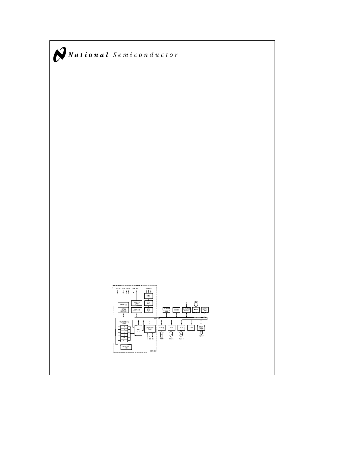
Block Diagram (HPC167064 with 16k EPROM shown)
Series 32000Éand TRI-STATEÉare registered trademarks of National Semiconductor Corporation.
MICROWIRE/PLUS
UNIX
IBM
É
SunOS
C
1995 National Semiconductor Corporation RRD-B30M105/Printed in U. S. A.
TM
is a registered trademark of AT & T Bell Laboratories.
É
and PC-ATÉare registered trademarks of International Business Machines Corp.
TM
and WATCHDOGTMare trademarks of National Semiconductor Corporation.
is a trademark of Sun Microsystems.
TL/DD11046
TL/DD/11046– 1
Page 2
Absolute Maximum Ratings
If Military/Aerospace specified devices are required,
please contact the National Semiconductor Sales
Office/Distributors for availability and specifications.
Total Allowable Source or Sink Current 100 mA
Storage Temperature Range
b
65§Ctoa150§C
Lead Temperature (Soldering, 10 sec.) 300§C
DC Electrical Characteristics
e
V
5.0Vg5% unless otherwise specified, T
CC
otherwise specified, T
e
0§Cto70§C for HPC467064
A
A
eb
V
with Respect to GND
CC
All Other Pins (V
Note:
Absolute maximum ratings indicate limits beyond
CC
a
which damage to the device may occur. DC and AC electrical specifications are not ensured when operating the device at absolute maximum ratings.
55§Ctoa125§C for HPC167064 and V
CC
e
Symbol Parameter Test Conditions Min Max Units
I
CC
I
CC
I
CC
Supply Current V
1
IDLE Mode Current V
2
HALT Mode Current V
3
e
CC
e
V
CC
e
V
CC
e
CC
e
V
CC
e
V
CC
e
CC
e
V
CC
max, f
max, f
max, f
max, f
max, f
max, f
max, f
2.5V, f
e
30.0 MHz (Note 1) 85 mA
IN
e
20.0 MHz (Note 1) 70 mA
IN
e
2.0 MHz (Note 1) 40 mA
IN
e
30.0 MHz (Note 1) 6.0 mA
IN
e
20.0 MHz, (Note 1) 4.5 mA
IN
e
2.0 MHz, (Note 1) 1 mA
IN
e
0 kHz, (Note 1) 400 mA
IN
e
0 kHz, (Note 1) 100 mA
IN
INPUT VOLTAGE LEVELS FOR SCHMITT TRIGGERED INPUTS RESET, NMI, AND WO; AND ALSO CKI
V
IH1 Logic High 0.9 V
V
IL1 Logic Low 0.1 V
ALL OTHER INPUTS
V
IH2
V
IL2
I
LI1
I
LI2
I
LI3
I
LI4
C
I
C
IO
Logic High 0.7 V
Logic Low * 0.2 V
Input Leakage Current V
Input Leakage Current RDY/HLD, EXUI V
e
0 and V
IN
e
0
IN
Input Leakage Current B12 RESETe0, V
Input Leakage Current EXM V
e
0 and V
IN
e
IN
e
IN
e
IN
VCC(Note 4)
V
CC
VCC(Note 4)
b
0.5 7 mA
g
Input Capacitance (Note 2) 10 pF
I/O Capacitance (Note 2) 20 pF
OUTPUT VOLTAGE LEVELS
V
OH1
V
OL1
V
OH2
V
OL2
V
OH3
V
OL3
V
OH4
V
OL4
V
OH5
V
OL5
V
RAM
I
OZ
Note 1: I
with NMI
Note 2: This is guaranteed by design and not tested.
Note 3: Test duration is 100 ms.
Note 4: The EPROM mode of operation for this device requires high voltage input on pins EXM/V
above the normal specification when driven to voltages greater than V
*See NORMAL RUNNING MODE.
Logic High (CMOS) I
Logic Low (CMOS) I
Port A/B Drive, CK2 I
(A0–A15, B10, B11, B12, B15) I
Other Port Pin Drive, WO (open drain) I
(B0–B9, B13, B14, P0 –P3) I
ST1 and ST2 Drive I
Port A/B Drive (A0–15, B10, B11, B12, B15) I
when used as External Address/Data Bus I
RAM Keep-Alive Voltage (Note 3) 2.5 V
TRI-STATEÉLeakage Current V
,I
,I
CC
1
e
measured with no external drive (IOHand I
CC
CC
2
3
VCC. CKI driven to V
and V
IH1
with rise and fall times less than 10 ns.
IL1
eb
10 mA (Note 2) V
OH
e
10 mA (Note 2)
OH
eb
7 mA 2.4
OH
e
3mA
OL
eb
1.6 mA (except WO) 2.4
OH
e
0.5 mA
OL
eb
6 mA 2.4
OH
e
I
1.6 mA
OL
eb
1 mA 2.4
OH
e
3mA
OL
e
0 and V
IN
e
e
0, IIH,I
OL
CC
IL
a
0.3V.
0 and EXMeVCC). I
e
V
IN
CC
is measured with RESETeGND. I
CC1
, I3, I4, I5, I6 and I7. This will increase the input leakage current
PP
CC
b
2
b
0.5V to 7.0V
0.5V) to (GNDb0.5V)
5.0Vg10% unless
CC
CC
CC
3
* V
CC
g
2 mA
b
50 mA
10 mA
0.1
0.1 V
0.4 V
0.4 V
0.4 V
0.4 V
CC
g
5 mA
is measured
CC3
V
V
V
V
Page 3
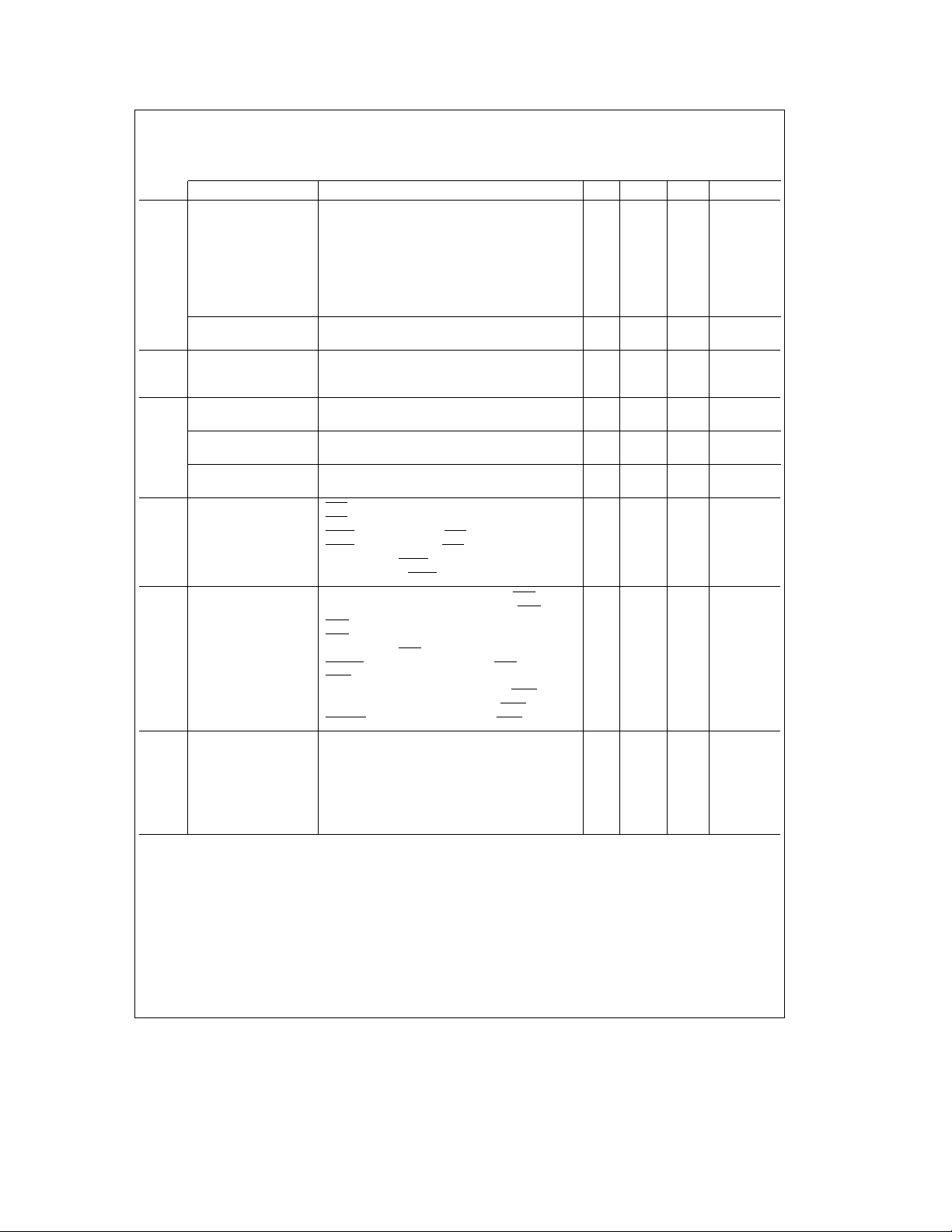
20 MHz
AC Electrical Characteristics
(See Notes 1 and 4 and
e
T
0§Ctoa70§C for HPC467064
A
Symbol and Formula Parameter Min Max Units Notes
f
C
e
t
C1
t
CKIH
t
CKIL
e
t
C
t
WAIT
ClocksTimersMicrowire/PlusExternal HoldUPI Timing
t
DC1C2R
t
DC1C2F
e
f
U
f
MW
e
f
XIN
e
t
XIN
Figures 1
thru5). V
CC
CKI Operating Frequency 2 20 MHz
1/f
C
CKI Clock Period 50 500 ns
CKI High Time 22.5 ns
CKI Low Time 22.5 ns
2/f
C
e
t
C
CPU Timing Cycle 100 ns
CPU Wait State Period 100 ns
Delay of CK2 Rising Edge after CKI Falling Edge 0 55 ns (Note 2)
Delay of CK2 Falling Edge after CKI Falling Edge 0 55 ns (Note 2)
fC/8 External UART Clock Input Frequency 2.5** MHz
External MICROWIRE/PLUS Clock Input Frequency 1.25 MHz
fC/22 External Timer Input Frequency 0.91 MHz
t
C
Pulse Width for Timer Inputs 100 ns
e
5Vg5%*,T
eb
55§Ctoa125§C for HPC167064 and V
A
CC
e
5Vg10%,
t
UWS
t
UWH
t
UWV
e
t
SALE
t
HWP
t
HAE
t
HAD
e
t
BF
e
t
BE
t
UAS
t
UAH
t
RPW
t
OE
t
OD
t
DRDY
t
WDW
t
UDS
t
UDH
t
UDH
t
A
*See NORMAL RUNNING MODE.
**This maximum frequency is attainable provided that this external baud clock has a duty cycle such that the high period includes two (2) falling edges of the CK2
clock.
e
Note: C
Note 1: These AC Characteristics are guaranteed with external clock drive on CKI having 50% duty cycle and with less than 15 pF load on CKO with rise and fall
times (t
Note 2: Do not design with this parameter unless CKI is driven with an active signal. When using a passive crystal circuit, its stability is not guaranteed if either CKI
or CKO is connected to any external logic other than the passive components of the crystal circuit.
Note 3: t
occurs later, t
Note 4: WS
with one wait state programmed.
Note 5: Due to emulation restrictionsÐactual limits will be better.
Note 6: Due to tester limitationsÐactual limits will be better.
40 pF.
L
and t
CKIR
CKIL
is spec’d for case with HLD falling edge occurring at the latest time can be accepted during the present CPU cycle being executed. If HLD falling edge
HAE
may be as long as (3t
HAE
e
t
WAIT
a
*/4 t
C
e
a
t
10 HLD Pulse Width 110 ns
C
e
a
t
100 HLDA Falling Edge after HLD Falling Edge 200 ns (Note 3)
C
e
a
*/4 t
85 HLDA Rising Edge after HLD Rising Edge 160 ns
C
a
(/2 t
66 Bus Float after HLDA Falling Edge 116 ns (Note 5)
C
a
(/2 t
66 Bus Enable after HLDA
C
(HPC467064) Input Data Hold after Rising Edge of UWR 20 ns
(HPC167064) 25* ns
) on CKI input less than 2.5 ns.
c
(number of pre-programmed wait states). Minimum and maximum values are calculated at maximum operating frequency, t
MICROWIRE Setup TimeÐMaster 100
MICROWIRE Setup TimeÐSlave 20
MICROWIRE Hold TimeÐMaster 20
MICROWIRE Hold TimeÐSlave 50
MICROWIRE Output Valid TimeÐMaster 50
MICROWIRE Output Valid TimeÐSlave 150
40 HLD Falling Edge before ALE Rising Edge 115 ns
Rising Edge 116 ns (Note 5)
Address Setup Time to Falling Edge of URD 10 ns
Address Hold Time from Rising Edge of URD 10 ns
URD Pulse Width 100 ns
URD Falling Edge to Output Data Valid 0 60 ns
Rising Edge of URD to Output Data Invalid 5 45 ns (Note 6)
RDRDY Delay from Rising Edge of URD 70 ns
UWR Pulse Width 40 ns
Input Data Valid before Rising Edge of UWR 10 ns
WRRDY Delay from Rising Edge of UWR 70 ns
a
C
4WSa72t
a
100) depending on the following CPU instruction cycles, its wait states and ready input.
C
ns
ns
ns
e
c
20.00 MHz,
3
Page 4
20 MHz
AC Electrical Characteristics
(See Notes 1 and 4 and
e
T
0§Ctoa70§C for HPC467064 (Continued)
A
Symbol and Formula Parameter Min Max Units Notes
t
DC1ALER
t
DC1ALEF
t
DC2ALER
t
DC2ALEF
e
t
LL
e
t
ST
Address CyclesRead CyclesWrite Cycles
Ready
Input
t
VP
t
ARR
t
ACC
t
RD
t
RW
t
DR
t
RDA
t
ARW
t
WW
t
V
t
HW
t
DAR
t
RWR
e
e
e
e
e
e
e
Figures 1
thru5.) V
CC
Delay from CKI Rising Edge to ALE Rising Edge 0 35 ns (Notes 1, 2)
Delay from CKI Rising Edge to ALE Falling Edge 0 35 ns (Notes 1, 2)
e
a
(/4 t
20 Delay from CK2 Rising Edge to ALE Rising Edge 45 ns
C
e
a
(/4 t
20 Delay from CK2 Falling Edge to ALE Falling Edge 45 ns
C
b
(/2 t
9 ALE Pulse Width 41 ns
C
b
(/4 t
7 Setup of Address Valid before ALE Falling Edge 18 ns
C
b
(/4 t
5 Hold of Address Valid after ALE Falling Edge 20 ns
C
e
b
(/4 t
5 ALE Falling Edge to RD Falling Edge 20 ns
C
e
aWSb
e
e
(/2 t
e
e
(/2 t
(/2 t
*/4 t
*/4 t
(/4 t
t
C
t
C
(/2 t
C
(/4 t
t
C
C
C
55 Data Input Valid after Address Output Valid 145 ns
aWSb
65 Data Input Valid after RD Falling Edge 85 ns
aWSb
C
b
b
C
C
aWSb
C
C
10 RD Pulse Width 140 ns
15 Hold of Data Input Valid after RD Rising Edge 0 60 ns
15 Bus Enable after RD Rising Edge 85 ns
b
5 ALE Falling Edge to WR Falling Edge 45 ns
aWSb
15 WR Pulse Width 160 ns
5 Data Output Valid before WR Rising Edge 145 ns
b
5 Hold of Data Valid after WR Rising Edge 20 ns
aWSb
50 Falling Edge of ALE to Falling Edge of RDY 75 ns
RDY Pulse Width 100 ns
(Continued)
e
5Vg5%*,T
eb
55§Ctoa125§C for HPC167064 and V
A
CC
e
5Vg10%,
4
Page 5
30 MHz
AC Electrical Characteristics
(See Notes 1 and 4 and
Symbol and Formula Parameter Min Max Units Notes
f
C
e
t
C1
t
CKIH
t
CKIL
e
2/f
t
C
e
t
WAIT
ClocksTimersMicrowire/PlusExternal HoldUPI TimingAddress Cycles
t
DC1C2R
t
DC1C2F
e
f
fC/8 External UART Clock Input Frequency 3.75** MHz
U
f
MW
e
f
XIN
e
t
XIN
Figures 1
thru5). V
CC
CKI Operating Frequency 2 30 MHz
1/f
C
CKI Clock Period 33 500 ns
CKI High Time 22.5 ns
CKI Low Time 22.5 ns
C
t
C
CPU Timing Cycle 66 ns
CPU Wait State Period 66 ns
Delay of CK2 Rising Edge after CKI Falling Edge 0 55 ns (Note 2)
Delay of CK2 Falling Edge after CKI Falling Edge 0 55 ns (Note 2)
External MICROWIRE/PLUS Clock Input Frequency 1.875 MHz
fC/22 External Timer Input Frequency 1.364 MHz
t
C
Pulse Width for Timer Inputs 66 ns
e
5Vg10%, T
e
0§Ctoa70§C for HPC467064.
A
t
UWS
t
UWH
t
UWV
t
SALE
t
HWP
e
t
HAE
t
HAD
e
t
BF
e
t
BE
t
UAS
t
UAH
t
RPW
t
OE
t
OD
t
DRDY
t
WDW
t
UDS
t
UDH
t
A
t
DC1ALER
t
DC1ALEF
t
DC2ALER
t
DC2ALEF
e
t
LL
e
t
ST
e
t
VP
MICROWIRE Setup TimeÐMaster 100
MICROWIRE Setup TimeÐSlave 20
MICROWIRE Hold TimeÐMaster 20
MICROWIRE Hold TimeÐSlave 50
MICROWIRE Output Valid TimeÐMaster 50
MICROWIRE Output Valid TimeÐSlave 150
e
a
*/4 t
40 HLD Falling Edge before ALE Rising Edge 90 ns
C
e
a
t
10 HLD Pulse Width 76 ns
C
a
t
85 HLDA Falling Edge after HLD Falling Edge 151 ns (Note 3)
C
e
a
*/4 t
85 HLDA
C
a
(/2 t
66 Bus Float after HLDA Falling Edge 99 ns (Note 5)
C
a
(/2 t
66 Bus Enable after HLDA Rising Edge 99 ns (Note 5)
C
Rising Edge after HLD Rising Edge 135 ns
Address Setup Time to Falling Edge of URD 10 ns
Address Hold Time from Rising Edge of URD 10 ns
URD Pulse Width 100 ns
URD Falling Edge to Output Data Valid 0 60 ns
Rising Edge of URD to Output Data Invalid 5 45 ns (Note 6)
RDRDY Delay from Rising Edge of URD 70 ns
UWR Pulse Width 40 ns
Input Data Valid before Rising Edge of UWR 10 ns
Input Data Hold after Rising Edge of UWR 20 ns
WRRDY Delay from Rising Edge of UWR 70 ns
Delay from CKI Rising Edge to ALE Rising Edge 0 35 ns (Notes 1, 2)
Delay from CKI Rising Edge to ALE Falling Edge 0 35 ns (Notes 1, 2)
e
a
(/4 t
20 Delay from CK2 Rising Edge to ALE Rising Edge 37 ns
C
e
a
(/4 t
20 Delay from CK2 Falling Edge to ALE Falling Edge 37 ns
C
b
(/2 t
9 ALE Pulse Width 24 ns
C
b
(/4 t
7 Setup of Address Valid before ALE Falling Edge 9 ns
C
b
(/4 t
5 Hold of Address Valid after ALE Falling Edge 11 ns
C
ns
ns
ns
5
Page 6
30 MHz
AC Electrical Characteristics
(See Notes 1 and 4 and
Figures 1
thru5). V
(Continued)
e
CC
5Vg10%, T
e
0§Ctoa70§C for HPC467064. (Continued)
A
Symbol and Formula Parameter Min Max Units Notes
e
t
ARR
t
ACC
t
RD
t
RW
Read CyclesWrite Cycles
t
DR
t
RDA
t
ARW
t
WW
e
t
V
t
HW
t
DAR
t
RWR
Input
Ready
**This maximum frequency is attainable provided that this external baud clock has a duty cycle such that the high period includes two (2) falling edges of the CK2
clock.
e
Note: C
Note 1: These AC Characteristics are guaranteed with external clock drive on CKI having 50% duty cycle and with less than 15 pF load on CKO with rise and fall
times (t
Note 2: Do not design with this parameter unless CKI is driven with an active signal. When using a passive crystal circuit, its stability is not guaranteed if either CKI
or CKO is connected to any external logic other than the passive components of the crystal circuit.
Note 3: t
occurs later, t
Note 4: WS
with one wait state programmed.
Note 5: Due to emulation restrictionsÐactual limits will be better.
Note 6: Due to tester limitationsÐactual limits will be better.
40 pF.
L
and t
CKIR
CKIL
is spec’d for case with HLD falling edge occurring at the latest time can be accepted during the present CPU cycle being executed. If HLD falling edge
HAE
may be as long as (3t
HAE
e
t
WAIT
b
(/4 t
5 ALE Falling Edge to RD Falling Edge 12 ns
C
e
aWSb
t
C
e
(/2 t
C
e
(/2 t
e
*/4 t
C
e
t
C
e
(/2 t
e
*/4 t
(/2 t
C
e
(/4 t
e
(/4 t
e
t
C
) on CKI input less than 2.5 ns.
c
(number of pre-programmed wait states). Minimum and maximum values are calculated at maximum operating frequency, t
32 Data Input Valid after Address Output Valid 100 ns
aWSb
C
b
b
C
C
aWSb
C
C
39 Data Input Valid after RD Falling Edge 60 ns
aWSb
14 RD Pulse Width 85 ns
15 Hold of Data Input Valid after RD Rising Edge 0 35 ns
15 Bus Enable after RD Rising Edge 51 ns
b
5 ALE Falling Edge to WR Falling Edge 28 ns
aWSb
15 WR Pulse Width 101 ns
5 Data Output Valid before WR Rising Edge 94 ns
b
10 Hold of Data Valid after WR Rising Edge 7 ns
aWSb
50 Falling Edge of ALE to Falling Edge of RDY 33 ns
RDY Pulse Width 66 ns
a
C
4WSa72t
a
100) depending on the following CPU instruction cycles, its wait states and ready input.
C
e
c
30.00 MHz,
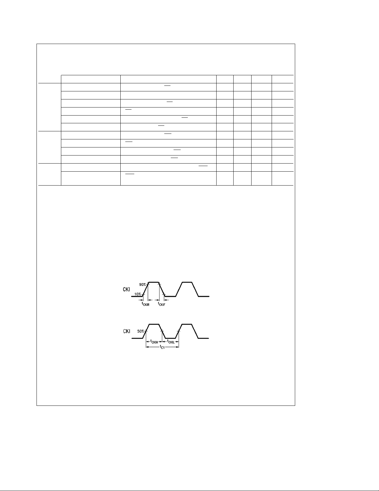
CKI Input Signal Characteristics
FIGURE 1. CKI Input Signal
Rise/Fall Time
TL/DD/11046– 2
Duty Cycle
TL/DD/11046– 3
6
Page 7
CKI Input Signal Characteristics
Note: AC testing inputs are driven at VIHfor logic ‘‘1’’ and VILfor a logic ‘‘0’’. Output timing measurements are made at VCC/2 for both logic ‘‘1’’ and logic ‘‘0’’.
FIGURE 2. Input and Output for AC Tests
TL/DD/11046– 4
Timing Waveforms
TL/DD/11046– 5
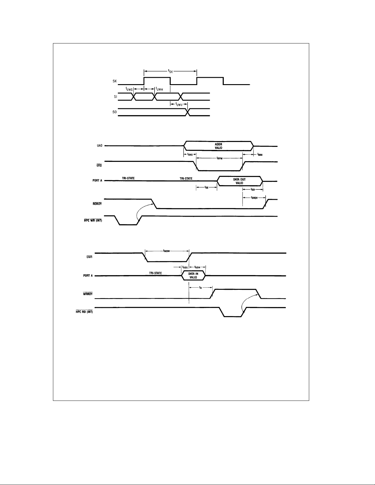
FIGURE 3. CK1, CK2, ALE Timing Diagram
TL/DD/11046– 6
FIGURE 4. Write Cycle
7
Page 8
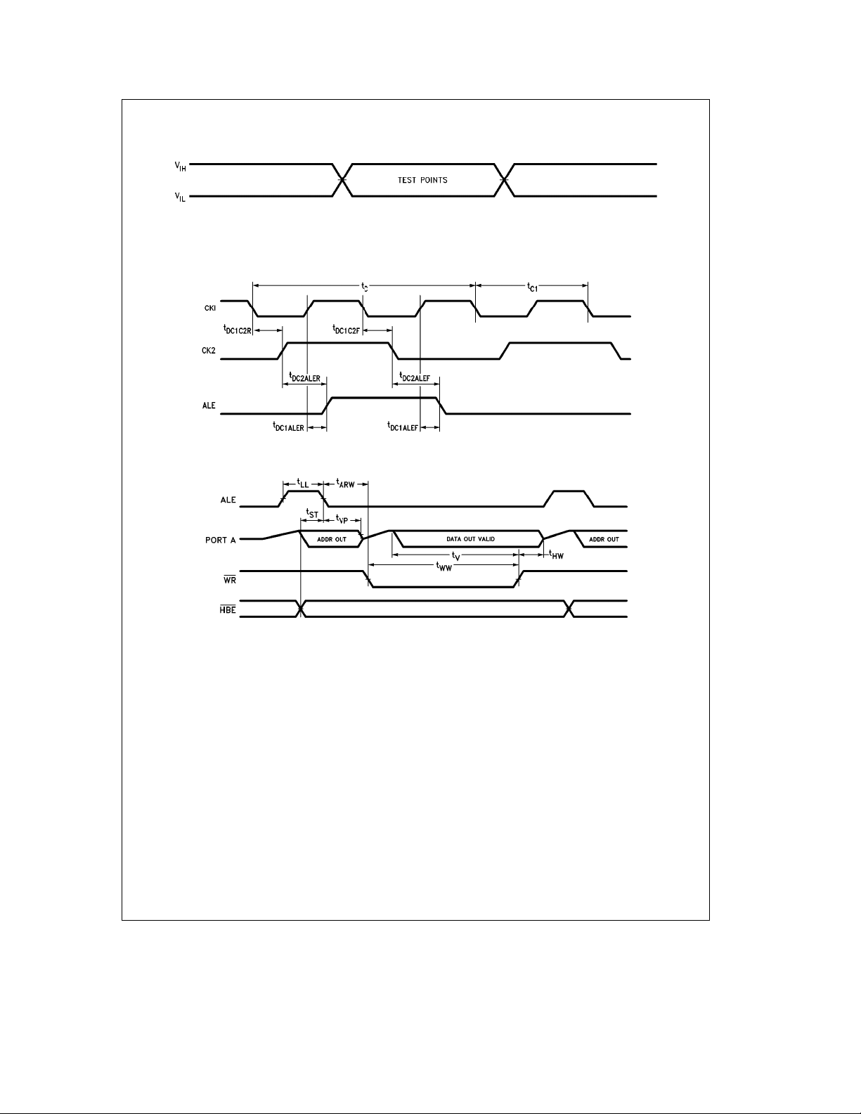
Timing Waveforms (Continued)
TL/DD/11046– 7
FIGURE 5. Read Cycle
TL/DD/11046– 8
FIGURE 6. Ready Mode Timing
FIGURE 7. Hold Mode Timing
8
TL/DD/11046– 9
Page 9
Timing Waveforms (Continued)
FIGURE 8. MICROWIRE Setup/Hold Timing
TL/DD/11046– 10
FIGURE 9. UPI Read Timing
FIGURE 10. UPI Write Timing
TL/DD/11046– 11
TL/DD/11046– 12
9
Page 10

Functional Modes of Operation
There are two primary functional modes of operation for the
HPC167064.
EPROM Mode
#
Normal Running Mode
#
EPROM MODE
In the EPROM mode, the HPC167064 is configured to ‘‘approximately emulate’’ a standard NMC27C256 EPROM.
Some dissimilarities do exist. The most significant one is
that HPC167064 contains only 16 kbytes of programmable
memory, rather than the 32 kbytes in 27C256. An
HPC167064 in the EPROM mode can be programmed with
a Data I/O machine.
Given below is the list of functions that can be performed by
the user in the EPROM mode.
Programming
#
CAUTION: Exceeding 14V on pin 1 (VPP) will damage the
HPC167064.
Initially, and after each erasure, all bits of the HPC
EPROM are in the ‘‘1’’ state. Data is introduced by selectively programming ‘‘0s’’ into the desired bit locations.
Although only ‘‘0s’’ will be programmed, both ‘‘1s’’ and
‘‘0s’’ can be presented in the data word. The only way to
change a ‘‘0’’ to a ‘‘1’’ is by ultraviolet light erasure.
Program/verify EPROM registers
#
To read data (verify) during the programming process,
V
must be at 13V. When reading data after the pro-
PP
gramming process, V
Program/verify ECON registers
#
There are two configuration registers ECON6 and
ECON7 to emulate different family members and also to
enable/disable different features in the chip. These registers are not mapped in the EPROM user space. These
bytes must be programmed through a pointer register
ECONA.
To prevent unintentional programming, the ECON6, 7
registers must be programmed with the assistance of this
pointer register. ECONA, and externally presented address, both identify the same ECON register may be programmed.
NORMAL RUNNING MODE
In this mode, the HPC167064 executes user software in the
normal manner. By default, its arcitecture imitates that of
the HPC16064. It may be configured to emulate the
HPC16083. The addressable memory map will be exactly as
for the HPC16083. The WATCHDOG function monitors addresses accordingly. Thus, the HPC167064 can be used as
a stand-alone emulator for both HPC16064 and HPC16083.
Within this mode, the on-chip EPROM cell acts as read only
memory. Each memory fetch is 16-bits wide. The
HPC167064 operates to 20 MHz with 1 wait state for the onchip memory.
can be either 13V or at VCC.
PP
The HPC167064 emulates the HPC16064 and HPC16083,
except as described here.
The value of EXM is latched on the rising edge of
#
RESET
. Thus, the user may not switch from ROMed to
ROMless operation or vice-versa, without another
RESET
pulse.
The security logic can be used to control access to the
#
on-chip EPROM. This feature is unique to the
HPC167064. There is no corresponding mode of operation on the HPC16064 or the HPC16083.
Specific inputs are allowed to be driven at high voltage
#
(13V) to configure the device for programming. These
high voltage inputs are unique to the HPC167064. The
same inputs cannot be driven to high voltage on the
HPC16064 and HPC16083 without damage to the part.
The Port D input structure on this device is slightly differ-
#
ent from the masked ROM HPC16083 and HPC16064.
V
min and V
IH2
ROM HPC16083 and HPC16064. There is a V
requirement for this device equal to V
is also a V
GND-0.05V. The V
the masked ROM devices is the Absolute Maximum Ratings of V
CC
The D.C. Electrical Characteristics and A.C. Electrical
#
Characteristics for the HPC167064, where T
a
to
125§C, are guaranteed over a reduced operating
voltage range of V
masked ROM devices that it simulates which is V
g
10%. These characteristics for the HPC467064, where
eb
T
0§Ctoa70§C, are guaranteed over the masked
A
ROM operating voltage range which is V
In addition to the reduced operating voltage range for the
#
HPC167064, the A.C. timing parameter t
to be a mimimum value of 25 ns. The masked ROM devices require a mimimum t
parameter for the HPC467064 is required to be the same
max are the same as for the masked
IL2
a
0.05V. There
min requirement for this device equal to
IL2
a
max and V
IH2
0.5V and GND-0.5V respectively.
g
5%. This is different from the
CC
UDH
CC
min requirement for
IL2
A
g
CC
is required
UDH
0f 20 ns. This A.C. timing
IH2
eb
10%.
max
55§C
as the masked ROM devices.
HPC167064 EPROM SECURITY
The HPC167064 includes security logic to provide READ
and WRITE protection of the on-chip EPROM. These defined privileges are intended to deter theft, alteration, or unintentional destruction of user code. Two bits are used to
define four levels of security on the HPC167064 to control
access to on-chip EPROM.
Security Level 3
This is the default configuration of an erased HPC167064.
READ and WRITE accesses to the on-chip EPROM or
ECON registers may be accomplished without constraint in
EPROM mode. READ accesses to the on-chip EPROM may
be accomplished without constraint in NORMAL RUNNING
mode.
CC
10
Page 11
Functional Modes of Operation (Continued)
Security Level 2
This security level prevents programming of the on-chip
EPROM or the ECON registers thereby providing WRITE
protection. Read accesses to the on-chip EPROM or ECON
registers may be accomplished without constraint in
EPROM. Read accesses to the on-chip EPROM may be
accomplished without constraint in NORMAL RUNNING
mode.
Security Level 1
This security level prevents programming of the on-chip
EPROM or ECON registersÐthereby providing registers
write protection. Read accesses to the on-chip ECON-registers may be accomplished without constraint in EPROM
mode. Read accesses to the on-chip EPROM will produce
ENCRYPTED data in EPROM. READ accesses to the onchip EPROM, during NORMAL RUNNING mode, are subject to Runtime Memory Protection. Under Runtime Memory Protection, only instruction opcodes stored within the
on-chip EPROM are allowed to access the EPROM as operand. If any other instruction opcode attempts to use the
contents of EPROM as an operand, it will receive the hex
value ‘‘FF’’. The Runtime Memory Protection feature is designed to prevent hostile software, running from external
memory or on-chip RAM, from reading secured EPROM
data. Transfers of control into, or out of the on-chip EPROM
(such as jump or branch) are not affected by Runtime Memory Protection. Interrupt vector fetches from EPROM proceed normally, and are not affected by Runtime Memory
Protection.
Security Level 0
This security level prevents programming of the on-chip
EPROM or ECON registers, thereby providing write protection. Read accesses to the on-chip ECON registers may be
accomplished without constraint in EPROM mode. READ
accesses to the on-chip EPROM are NOT ALLOWED in
EPROM mode. Such accesses will return data value ‘‘FF’’
hex. Runtime Memory Protection is enforced as in security
level 1.
These four levels of security help ensure that the user
EPROM code is not tampered with in a test fixture and that
code executing from RAM or external memory does not
dump the user algorithm.
Erasure Characteristics
The erasure characteristics of the HPC167064 are such that
erasure begins to occur when exposed to light with wavelengths shorter than approximately 4000 Angstroms (Ð). It
should be noted that sunlight and certain types of fluorescent lamps have wavelengths in the 3000Ж4000Рrange.
After programming, opaque labels should be placed over
the HPC167064’s window to prevent unintentional erasure.
Covering the window will also prevent temporary functional
failure due to the generation of photo currents.
The recommended erasure procedure for the HPC167064 is
exposure to short wave ultraviolet light which has a wavelength of 2537 Angstroms (Ð). The integrated dose (i.e., UV
c
intensity
of 30W-sec/cm
The HPC167064 should be placed within 1 inch of the lamp
tubes during erasure. Some lamps have a filter on their
tubes which should be removed before erasure. The erasure time table shows the minimum HPC167064 erasure
time for various light intensities.
exposure time) for erasure should be a minimum
2
.
An erasure system should be calibrated periodically. The
distance from lamp to unit should be maintained at one inch.
The erasure time increases as the square of the distance. (If
distance is doubled the erasure time increases by a factor of
4.) Lamps lose intensity as they age. When a lamp is
changed, the distance has changed or the lamp has aged,
the system should be checked to make certain full erasure
is occurring.
Incomplete erasure will cause symptoms that can be misleading. Programmers, components, and even system designs have been erroneously suspected when incomplete
erasure was the problem.
Minimum HPC167064 Erasure Time
Light Intensity Erasure Time
(Micro-Watts/cm
15,000 36
10,000 50
2
) (Minutes)
Memory Map of the HPC167064
The HPC167064 has 256 bytes of on-chip user RAM and
chip registers located at address 0000 –01FF that is always
enabled, and 256 bytes of on-chip RAM located at 0200 –
02FF that can be enabled or disabled. It has 8 kbytes of onchip EPROM located at address 0E000 – 0FFFF that is always enabled and 8 kbytes of EPROM located at address
0C000–0DFFF that can be enabled or disabled.
The ECON6 contains two bits ROM0 and RAM0. When
these bits are ‘‘1’’ (erased default), full 16 kbytes of ROM
and 512 bytes of RAM are enabled. Programming a ‘‘0’’ to
these bits disables the lower 8k for the EPROM and upper
256 bytes for the RAM. The ECON registers are only accessible to the user during EPROM mode.
Address In Address In Other
EPROM Mode HPC Modes
7FFF Operation
4000 FFFF
3FFF
2000 E000
1FFF DFFF
0000 C000
11
–
Enabled or
Disabled by
config logic
Page 12

Pin Descriptions
The HPC167064 is available only in 68-pin LDCC package.
I/O PORTS
Port A is a 16-bit bidirectional I/O port with a data direction
register to enable each separate pin to be individually defined as an input or output. When accessing external memory, port A is used as the multiplexed address/data bus.
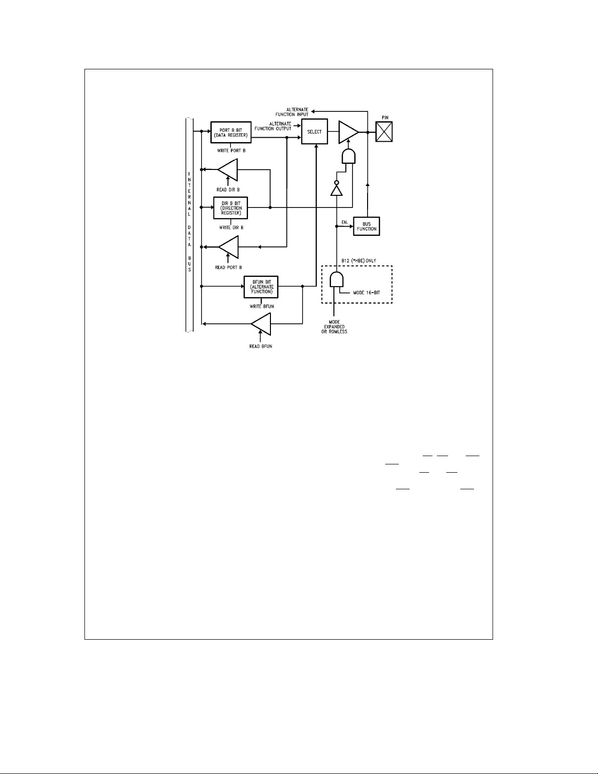
Port B is a 16-bit port with 12 bits of bidirectional I/O similar
in structure to Port A. Pins B10, B11, B12 and B15 are general purpose outputs only in this mode. Port B may also be
configured via a 16-bit function register BFUN to individually
allow each pin to have an alternate function.
B0: TDX UART Data Output
B1:
B2: CKX UART Clock (Input or Output)
B3: T2IO Timer2 I/O Pin
B4: T3IO Timer3 I/O Pin
B5: SO MICROWIRE/PLUS Output
B6: SK MICROWIRE/PLUS Clock (Input or Output)
B7: HLDA
B8: TS0 Timer Synchronous Output
B9: TS1 Timer Synchronous Output
B10: UA0 Address 0 Input for UPI Mode
B11: WRRDY
B12:
B13: TS2 Timer Synchronous Output
B14: TS3 Timer Synchronous Output
B15: RDRDY
When accessing external memory, four bits of port B are
used as follows:
B10: ALE Address Latch Enable Output
B11: WR
B12: HBE
B15: RD
Port I is an 8-bit input port that can be read as general
purpose inputs and is also used for the following functions:
I0:
I1: NMI Nonmaskable Interrupt Input
I2: INT2 Maskable Interrupt/Input Capture/URD
I3: INT3 Maskable Interrupt/Input Capture/UWR
I4: INT4 Maskable Interrupt/Input Capture
I5: SI MICROWIRE/PLUS Data Input
I6: RDX UART Data Input
I7:
Port D is an 8-bit input port that can be used as general
purpose digital inputs.
Port P is a 4-bit output port that can be used as general
purpose data, or selected to be controlled by timers 4
through 7 in order to generate frequency, duty cycle and
pulse width modulated outputs.
Hold Acknowledge Output
Write Ready Output for UPI Mode
Read Ready Output for UPI Mode
Write Output
High Byte Enable Output/Input
(sampled at reset)
Read Output
POWER SUPPLY PINS
V
and
CC1
V
Positive Power Supply
CC2
GND Ground for On-Chip Logic
DGND Ground for Output Buffers
Note: There are two electrically connected VCCpins on the chip, GND and
DGND are electrically isolated. Both V
must be used.
pins and both ground pins
CC
CLOCK PINS
CKI The Chip System Clock Input
CKO The Chip System Clock Output (inversion of CKI)
Pins CKI and CKO are usually connected across an external
crystal.
CK2 Clock Output (CKI divided by 2)
OTHER PINS
WO
This is an active low open drain output that signals an illegal situation has been detected by the
WATCHDOG logic.
ST1 Bus Cycle Status Output: indicates first opcode
fetch.
ST2 Bus Cycle Status Output: indicates machine
states (skip, interrupt and first instruction cycle).
RESET
is an active low input that forces the chip to restart and sets the ports in a TRI-STATE mode.
RDY/HLD
has two uses, selected by a software bit. It’s either an input to extend the bus cycle for slower
memories, or a HOLD request input to put the
bus in a high impedance state for DMA purposes.
NC (no connection) do not connect anything to this
pin.
EXM Has two uses. External memory enable (active
high) which disables internal EPROM and maps
it to external memory, and is V
mode.
during EPROM
PP
EI External interrupt with vector address
FFF1:FFF0. (Rising/falling edge or high/low level sensitive). Alternately can be configured as
4th input capture.
EXUI
External interrupt which is internally OR’ed with
the UART interrupt with vector address
FFF3:FFF2 (Active Low).
12
Page 13

Connection Diagram
Order Number HPC167064, EL
See NS Package Number EL68C
PortsA&B
The highly flexible A and B ports are similarly structured.
The Port A (see
direction register. Port B (see
an alternate function register in addition to the data and
direction registers. All the control registers are read/write
registers.
The associated direction registers allow the port pins to be
individually programmed as inputs or outputs. Port pins selected as inputs are placed in a TRI-STATE mode by resetting corresponding bits in the direction register.
Figure 11
), consists of a data register and a
Figures 12
thru
Figure 14
) has
Top View
TL/DD/11046– 17
A write operation to a port pin configured as an input causes
the value to be written into the data register, a read operation returns the value of the pin. Writing to port pins configured as outputs causes the pins to have the same value,
reading the pins returns the value of the data register.
Primary and secondary functions are multiplexed onto Port
B through the alternate function register (BFUN). The secondary functions are enabled by setting the corresponding
bits in the BFUN register.
FIGURE 11. Port A: I/O Structure
13
TL/DD/11046– 19
Page 14

PortsA&B(Continued)
FIGURE 12. Structure of Port B Pins B0, B1, B2, B5, B6 and B7 (Typical Pins)
TL/DD/11046– 20
FIGURE 13. Structure of Port B Pins B3, B4, B8, B9, B13 and B14 (Timer Synchronous Pins)
TL/DD/11046– 21
14
Page 15
PortsA&B(Continued)
FIGURE 14. Structure of Port B Pins B10, B11, B12 and B15 (Pins with Bus Control Roles)
Operating Modes
To offer the user a variety of I/O and expanded memory
options, the HPC167064 has four operating modes. The
various modes of operation are determined by the state of
both the EXM pin and the EA bit in the PSW register. The
state of the EXM pin determines whether on-chip EPROM
will be accessed or external memory will be accessed within
the address range of the on-chip EPROM. The on-chip
EPROM range of the HPC167064 is C000 to FFFF
(16 kbytes).
A logic ‘‘0’’ state on the EXM pin will cause the HPC device
to address on-chip EPROM when the Program Counter (PC)
contains addresses within the on-chip EPROM address
range. A logic ‘‘1’’ state on the EXM pin will cause the HPC
device to address memory that is external to the HPC when
the PC contains on-chip EPROM addresses. The function of
the EA bit is to determine the legal addressing range of the
HPC device. A logic ‘‘0’’ state in the EA bit of the PSW
register does two thingsÐaddresses are limited to the onchip EPROM range and on-chip RAM and Register range,
and the ‘‘illegal address detection’’ feature of the WATCH-
TL/DD/11046– 22
DOG logic is engaged. A logic ‘‘1’’ in the EA bit enables
accesses to be made anywhere within the 64 kbytes address range and the ‘‘illegal address detection’’ feature of
the WATCHDOG logic is disabled.
All HPC devices can be used with external memory. External memory may be any combination of RAM and EPROM.
Both 8-bit and 16-bit external data bus modes are available.
Upon entering an operating mode in which external memory
is used, Port A becomes the Address/Data bus. Four pins of
Port B become the control lines ALE, RD
The High Byte Enable pin (HBE
select high order memory bytes. The RD
are only generated if the selected address is off-chip. The 8bit mode is selected by pulling HBE
left floating or connected to a memory device chip select at
reset, the 16-bit mode is entered. The following sections
describe the operating modes of the HPC167064.
Note: The HPC devices use 16-bit words for stack memory. Therefore,
when using the 8-bit mode, User’s Stack must be in internal RAM.
) is used in 16-bit mode to
,WRand HBE.
and WR signals
high at reset. If HBE is
15
Page 16
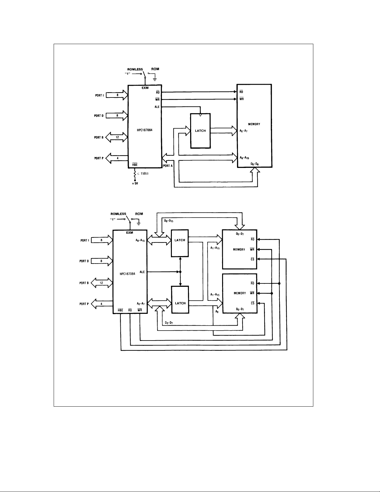
HPC167064 Operating Modes
SINGLE CHIP NORMAL MODE
In this mode, the HPC167064 functions as a self-contained
microcomputer (see
EPROM) on-chip. It can address internal memory only, consisting of 16 kbytes of EPROM (C000 to FFFF) and
512 bytes of on-chip RAM and Registers (0000 to 02FF).
The ‘‘illegal address detection’’ feature of the WATCHDOG
is enabled in the Single-Chip Normal mode and a WATCHDOG Output (WO
addresses that are outside of the on-chip EPROM and RAM
range of the device. Ports A and B are used for I/O functions and not for addressing external memory. The EXM pin
and the EA bit of the PSW register must both be logic ‘‘0’’ to
enter the Single-Chip Normal mode.
EXPANDED NORMAL MODE
The Expanded Normal mode of operation enables the
HPC167064 to address external memory in addition to the
on-chip ROM and RAM (see Table I). WATCHDOG illegal
address detection is disabled and memory accesses may
be made anywhere in the 64 kbyte address range without
triggering an illegal address condition. The Expanded Normal mode is entered with the EXM pin pulled low (logic ‘‘0’’)
and setting the EA bit in the PSW register to ‘‘1’’.
TABLE I. HPC167064 Operating Modes
Operating Mode
Single-Chip Normal 0 0 C000– FFFF On-Chip
Expanded Normal
Single-Chip ROMless 1 0 C000–FFFF Off-Chip
Expanded ROMless 1 1 0300– FFFF Off-Chip
SINGLE-CHIP ROMless MODE
In this mode, the on-chip EPROM of the HPC167064 is not
used. The address space corresponding to the on-chip
EPROM is mapped into external memory so 16k of external
memory may be used with the HPC167064 (see Table I).
The WATCHDOG circuitry detects illegal addresses (addresses not within the on-chip EPROM and RAM range).
The Single-Chip ROMless mode is entered when the EXM
pin is pulled high (logic ‘‘1’’) and the EA bit is logic ‘‘0’’.
EXPANDED ROM MODE
This mode of operation is similar to Single-Chip ROMless
mode in that no on-chip ROM is used, however, a full
64 kbytes of external memory may be used. The ‘‘illegal
address detection’’ feature of WATCHDOG is disabled. The
EXM pin must be pulled high (logic ‘‘1’’) and the EA bit in the
PSW register set to ‘‘1’’ to enter this mode.
Figure 15
) will occur if an attempt is made to access
) with all memory (RAM and
EXM EA Memory
Pin Bit Configuration
01
C000–FFFF On-Chip
0300–BFFF Off-Chip
Wait States
The internal EPROM can be accessed at the maximum operating frequency with one wait state. With 0 wait states,
internal ROM accesses are limited to )/3 f
HPC167064 provides four software selectable Wait States
that allow access to slower memories. The Wait States are
selected by the state of two bits in the PSW register. Additionally, the RDY input may be used to extend the instruction cycle, allowing the user to interface with slow memories
and peripherals.
max. The
C
FIGURE 15. Single-Chip Mode
TL/DD/11046– 23
Power Save Modes
Two power saving modes are available on the HPC167064:
HALT and IDLE. In the HALT mode, all processor activities
are stopped. In the IDLE mode, the on-board oscillator and
timer T0 are active but all other processor activities are
stopped. In either mode, all on-board RAM, registers and
I/O are unaffected.
HALT MODE
The HPC167064 is placed in the HALT mode under software control by setting bits in the PSW. All processor activities, including the clock and timers, are stopped. In the
HALT mode, power requirements for the HPC167064 are
minimal and the applied voltage (V
without altering the state of the machine. There are two
ways of exiting the HALT mode: via the RESET
The RESET
input will generate a vectored interrupt and resume operation from that point with no initialization. The HALT mode
can be enabled or disabled by means of a control register
HALT enable. To prevent accidental use of the HALT mode
the HALT enable register can be modified only once.
IDLE MODE
The HPC167064 is placed in the IDLE mode through the
PSW. In this mode, all processor activity, except the onboard oscillator and Timer T0, is stopped. As with the HALT
mode, the processor is returned to full operation by the
RESET
lization. A timer T0 overflow will also cause the HPC167064
to resume normal operation.
Note: If an NMI interrupt is received during the instruction which puts the
input reinitializes the processor. Use of the NMI
or NMI inputs, but without waiting for oscillator stabi-
device in Halt or Idle Mode, the device will enter that power saving
mode. The interrupt will be held pending until the device exits that
power saving mode. When exiting Idle mode via the T0 overflow, the
NMI interrupt will be serviced when the device exits Idle. If another
NMI interrupt is received during either Halt of Idle the processor will
exit the power saving mode and vector to the interrupt address.
) may be decreased
CC
or the NMI.
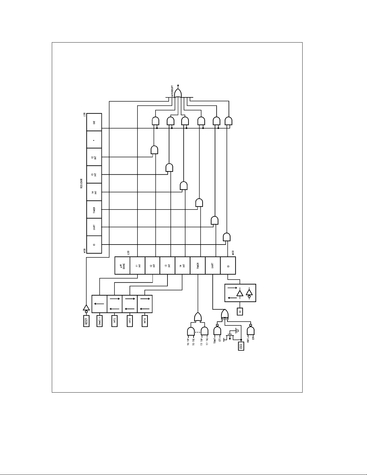
HPC167064 Interrupts
Complex interrupt handling is easily accomplished by the
HPC167064’s vectored interrupt scheme. There are eight
possible interrupt sources as shown in Table II.
16
Page 17
HPC167064 Interrupts (Continued)
FIGURE 16. 8-Bit External Memory
FIGURE 17. 16-Bit External Memory
TL/DD/11046– 24
TL/DD/11046– 25
17
Page 18
HPC167064 Interrupts (Continued)
TABLE II. Interrupts
Vector
Address Ranking
FFFF:FFFE RESET 0
FFFD:FFFC Nonmaskable external on rising edge of I1 pin 1
FFFB:FFFA External interrupt on I2 pin 2
FFF9:FFF8 External interrupt on I3 pin 3
FFF7:FFF6 External interrupt on I4 pin 4
FFF5:FFF4 Overflow on internal timers 5
FFF3:FFF2 Internal on the UART transmit/receive complete or external on EXUI 6
FFF1:FFF0 External interrupt on EI pin 7
Interrupt Source
Arbitration
Interrupt Arbitration
The HPC167064 contains arbitration logic to determine
which interrupt will be serviced first if two or more interrupts
occur simultaneously. The arbitration ranking is given in Table II. The interrupt on RESET
serviced first.
has the highest rank and is
Interrupt Processing
Interrupts are serviced after the current instruction is completed except for the RESET
RESET
and EXUI are level-LOW-sensitive interrupts and EI
is programmable for edge-(RISING or FALLING) or level(HIGH or LOW) sensitivity. All other interrupts are edge-sensitive. NMI is positive-edge sensitive. The external interrupts
on I2, I3 and I4 can be software selected to be rising or
falling edge. External interrupt (EXUI
interrupt. This interrupt is level-low sensitive. To select this
interrupt disable the ERI and ETI UART interrupt bits in the
ENUI register. To select the UART interrupt leave this pin
floating or tie it high.
, which is serviced immediately.
) is shared with UART
Interrupt Control Registers
The HPC167064 allows the various interrupt sources and
conditions to be programmed. This is done through the various control registers. A brief description of the different control registers is given below.
INTERRUPT ENABLE REGISTER (ENIR)
RESET
and the External Interrupt on I1 are non-maskable
interrupts. The other interrupts can be individually enabled
or disabled. Additionally, a Global Interrupt Enable Bit in the
ENIR Register allows the Maskable interrupts to be collectively enabled or disabled. Thus, in order for a particular
interrupt to request service, both the individual enable bit
and the Global Interrupt bit (GIE) have to be set.
INTERRUPT PENDING REGISTER (IRPD)
The IRPD register contains a bit allocated for each interrupt
vector. The occurrence of specified interrupt trigger conditions causes the appropriate bit to be set. There is no indication of the order in which the interrupts have been received. The bits are set independently of the fact that the
interrupts may be disabled. IRPD is a Read/Write register.
The bits corresponding to the maskable, external interrupts
are normally cleared by the HPC167064 after servicing the
interrupts.
For the interrupts from the on-board peripherals, the user
has the responsibility of resetting the interrupt pending flags
through software.
The NMI bit is read only and I2, I3, and I4 are designed as to
only allow a zero to be written to the pending bit (writing a
one has no affect). A LOAD IMMEDIATE instruction is to be
the only instruction used to clear a bit or bits in the IRPD
register. This allows a mask to be used, thus ensuring that
the other pending bits are not affected.
INTERRUPT CONDITION REGISTER (IRCD)
Three bits of the register select the input polarity of the
external interrupt on I2, I3, and I4.
Servicing the Interrupts
The Interrupt, once acknowledged, pushes the program
counter (PC) onto the stack thus incrementing the stack
pointer (SP) twice. The Global Interrupt Enable bit (GIE) is
copied into the CGIE bit of the PSW register; it is then reset,
thus disabling further interrupts. The program counter is
loaded with the contents of the memory at the vector address and the processor resumes operation at this point. At
the end of the interrupt service routine, the user does a
RETI instruction to pop the stack and re-enable interrupts if
the CGIE bit is set, or RET to just pop the stack if the CGIE
bit is clear, and then returns to the main program. The GIE
bit can be set in the interrupt service routine to nest interrupts if desired.
Figure 18
shows the Interrupt Enable Logic.
RESET
The RESET input initializes the processor and sets Ports A
and B in the TRI-STATE condition and Port P in the LOW
state. RESET
processor vectors to FFFF:FFFE and resumes operation at
the address contained at that memory location (which must
correspond to an on board location). The Reset vector address must be between C000 and FFFF when emulating the
HPC16064 and between E000 and FFFF when emulating
the HPC16003.
is an active-low Schmitt trigger input. The
Timer Overview
The HPC167064 contains a powerful set of flexible timers
enabling the HPC167064 to perform extensive timer functions not usually associated with microcontrollers. The
HPC167064 contains nine 16-bit timers. Timer T0 is a
free-running timer, counting up at a fixed CKI/16
18
Page 19
TL/DD/11046– 26
FIGURE 18. Block Diagram of Interrupt Logic
19
Page 20
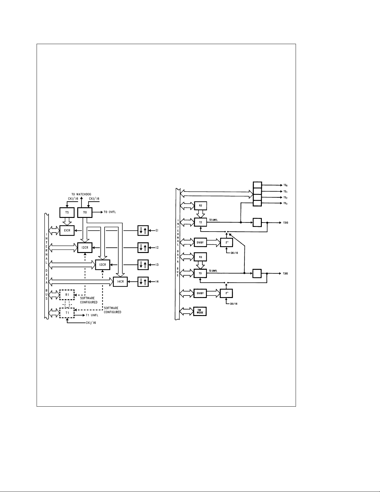
Timer Overview (Continued)
(Clock Input/16) rate. It is used for WATCHDOG logic, high
speed event capture, and to exit from the IDLE mode. Consequently, it cannot be stopped or written to under software
control. Timer T0 permits precise measurements by means
of the capture registers I2CR, I3CR, and I4CR. A control bit
in the register TMMODE configures timer T1 and its associated register R1 as capture registers I3CR and I2CR. The
capture registers I2CR, I3CR, and I4CR respectively, record
the value of timer T0 when specific events occur on the
interrupt pins I2, I3, and I4. The control register IRCD programs the capture registers to trigger on either a rising edge
or a falling edge of its respective input. The specified edge
can also be programmed to generate an interrupt (see
ure 19
).
The HPC167064 provides an additional 16-bit free running
timer, T8, with associated input capture register EICR (External Interrupt Capture Register) and Configuration Register, EICON. EICON is used to select the mode and edge of
the EI pin. EICR is a 16-bit capture register which records
the value of T8 (which is identical to T0) when a specific
event occurs on the EI pin.
The timers T2 and T3 have selectable clock rates. The
clock input to these two timers may be selected from the
following two sources: an external pin, or derived internally by
Fig-
dividing the clock input. Timer T2 has additional capability of
being clocked by the timer T3 underflow. This allows the
user to cascade timers T3 and T2 into a 32-bit timer/counter. The control register DIVBY programs the clock input to
timers T2 and T3 (see
The timers T1 through T7 in conjunction with their registers
form Timer-Register pairs. The registers hold the pulse duration values. All the Timer-Register pairs can be read from
or written to. Each timer can be started or stopped under
software control. Once enabled, the timers count down, and
upon underflow, the contents of its associated register are
automatically loaded into the timer.
SYNCHRONOUS OUTPUTS
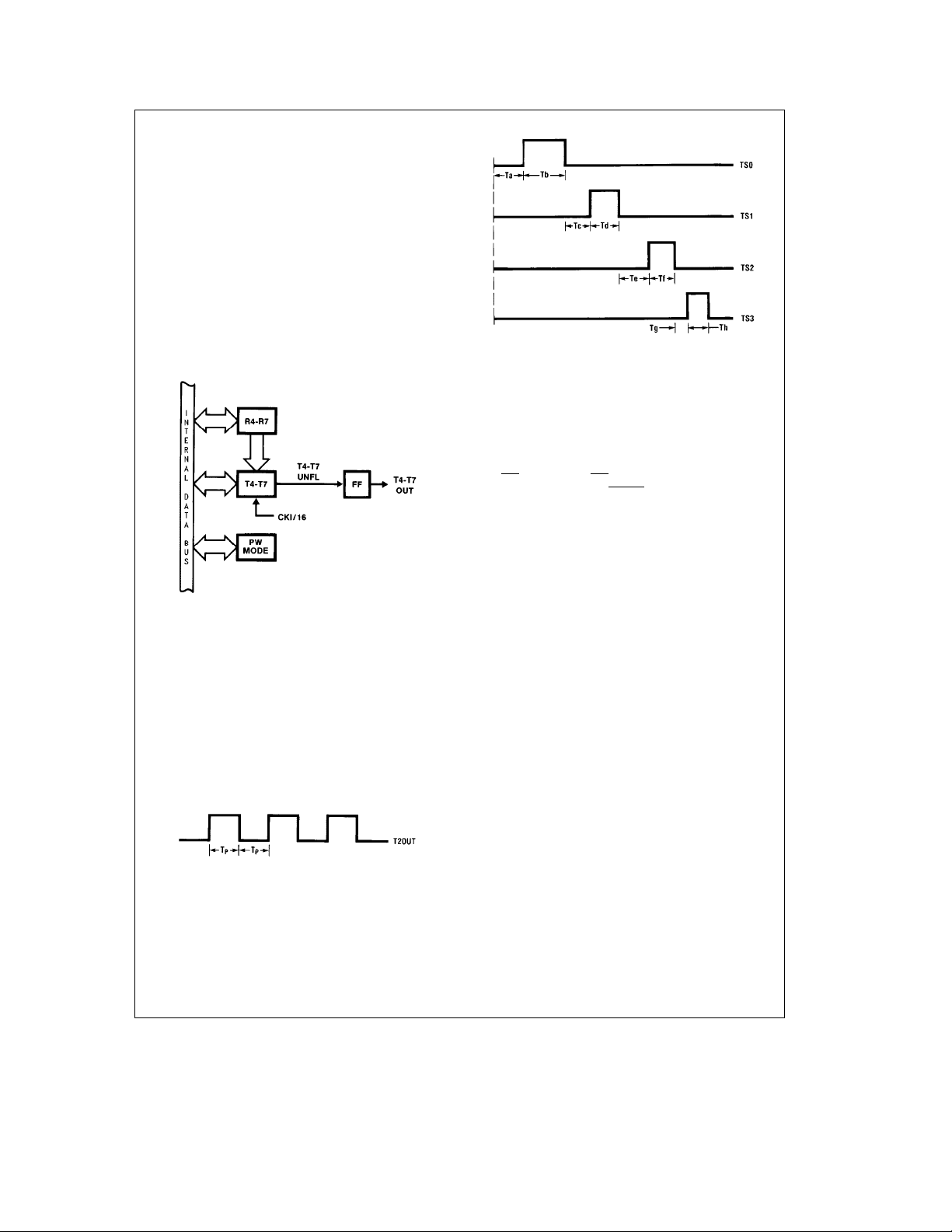
The flexible timer structure of the HPC167064 simplifies
pulse generation and measurement. There are four synchronous timer outputs (TS0 through TS3) that work in conjunction with the timer T2. The synchronous timer outputs
can be used either as regular outputs or individually programmed to toggle on timer T2 underflows (see
Timer/register pairs 4–7 form four identical units which can
generate synchronous outputs on Port P (see
Figure 20
).
Figure 20
Figure 21
).
).
FIGURE 19. Timers T0, T1 and T8
with Four Input Capture Registers
TL/DD/11046– 27
FIGURE 20. Timers T2–T3 Block
TL/DD/11046– 28
20
Page 21
Timer Overview (Continued)
Maximum output frequency for any timer output can be obtained by setting timer/register pair to zero. This then will
produce an output frequency equal to (/2 the frequency of
the source used for clocking the timer.
Timer Registers
There are four control registers that program the timers. The
divide by (DIVBY) register programs the clock input to timers T2 and T3. The timer mode register (TMMODE) contains
control bits to start and stop timers T1 through T3. It also
contains bits to latch, acknowledge and enable interrupts
from timers T0 through T3. The control register PWMODE
similarly programs the pulse width timers T4 through T7 by
allowing them to be started, stopped, and to latch and enable interrupts on underflows. The PORTP register contains
bits to preset the outputs and enable the synchronous timer
output functions.
FIGURE 21. Timers T4–T7 Block
TL/DD/11046– 29
Timer Applications
The use of Pulse Width Timers for the generation of various
waveforms is easily accomplished by the HPC167064.
Frequencies can be generated by using the timer/register
pairs. A square wave is generated when the register value is
a constant. The duty cycle can be controlled simply by
changing the register value.
Synchronous outputs based on Timer T2 can be generated
on the 4 outputs TS0 –TS3. Each output can be individually
programmed to toggle on T2 underflow. Register R2 contains the time delay between events.
ple of synchronous pulse train generation.
FIGURE 22. Square Wave Frequency Generation
Figure 23
is an exam-
TL/DD/11046– 31
WATCHDOG Logic
The WATCHDOG Logic monitors the operations taking
place and signals upon the occurrence of any illegal activity.
FIGURE 23. Synchronous Pulse Generation
The illegal conditions that trigger the WATCHDOG logic are
potentially infinite loops and illegal addresses. Should the
WATCHDOG register not be written to before Timer T0
overflows twice, or more often than once every 4096
counts, an infinite loop condition is assumed to have occurred. An illegal condition also occurs when the processor
generates an illegal address when in the Single-Chip
modes.* Any illegal condition forces the WATCHDOG Output (WO
) pin low. The WO pin is an open drain output and
can be connected to the RESET
users external logic.
*Note: See Operating Modes for details.
or NMI inputs or to the
TL/DD/11046– 30
MICROWIRE/PLUS
MICROWIRE/PLUS is used for synchronous serial data
communications (see
an 8-bit parallel-loaded, serial shift register using SI as the
input and SO as the output. SK is the clock for the serial
shift register (SIO). The SK clock signal can be provided by
an internal or external source. The internal clock rate is programmable by the DIVBY register. A DONE flag indicates
when the data shift is completed.
The MICROWIRE/PLUS capability enables it to interface
with any of National Semiconductor’s MICROWIRE peripherals (i.e., A/D converters, display drivers, EEPROMs).
Figure 24
). MICROWIRE/PLUS has
MICROWIRE/PLUS Operation
The HPC167064 can enter the MICROWIRE/PLUS mode
as the master or a slave. A control bit in the IRCD register
determines whether the HPC167064 is the master or slave.
The shift clock is generated when the HPC167064 is configured as a master. An externally generated shift clock on the
SK pin is used when the HPC167064 is configured as a
slave. When the HPC167064 is a master, the DIVBY register programs the frequency of the SK clock. The DIVBY
register allows the SK clock frequency to be programmed in
15 selectable steps from 64 Hz to 1 MHz with CKI at
16.0 MHz.
The contents of the SIO register may be accessed through
any of the memory access instructions. Data waiting to be
transmitted in the SIO register is clocked out on the falling
edge of the SK clock. Serial data on the SI pin is clocked in
on the rising edge of the SK clock.
21
Page 22
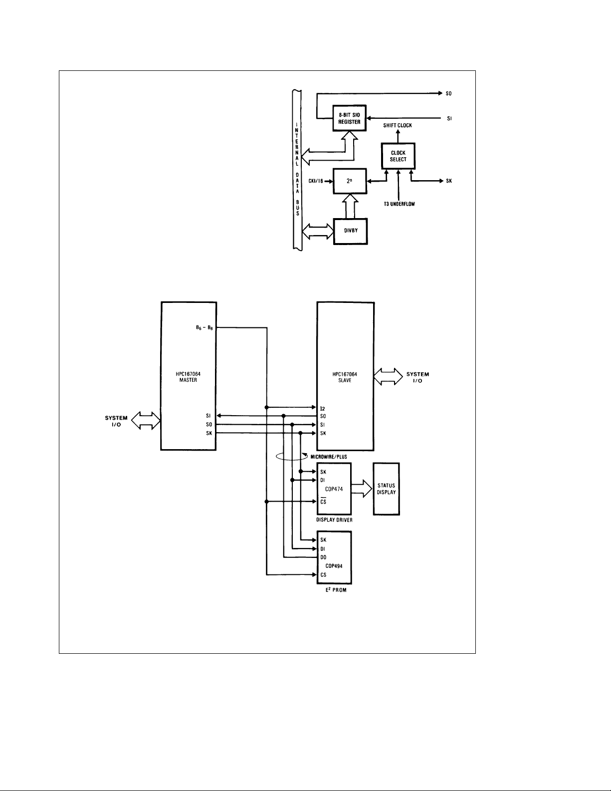
MICROWIRE/PLUS Application
Figure 25
an automotive application. The microcontroller-based system could be used to interface to an instrument cluster and
various parts of the automobile. The diagram shows two
HPC167064 microcontrollers interconnected to other
MICROWIRE peripherals. HPC167064 1 is set up as the
master and initiates all data transfers. HPC167064 2 is set
up as a slave answering to the master.
The master microcontroller interfaces the operator with the
system and could also manage the instrument cluster in an
automotive application. Information is visually presented to
the operator by means of a LCD display controlled by the
COP472 display driver. The data to be displayed is sent
serially to the COP472 over the MICROWIRE/PLUS link.
Data such as accumulated mileage could be stored and retrieved from the EEPROM COP494. The slave HPC167064
could be used as a fuel injection processor and generate
timing signals required to operate the fuel valves. The master processor could be used to periodically send updated
values to the slave via the MICROWIRE/PLUS link. To
speed up the response, chip select logic is implemented by
connecting an output from the master to the external interrupt input on the slave.
illustrates a MICROWIRE/PLUS arrangement for
FIGURE 24. MICROWIRE/PLUS
TL/DD/11046– 32
FIGURE 25. MICROWIRE/PLUS Application
22
TL/DD/11046– 33
Page 23
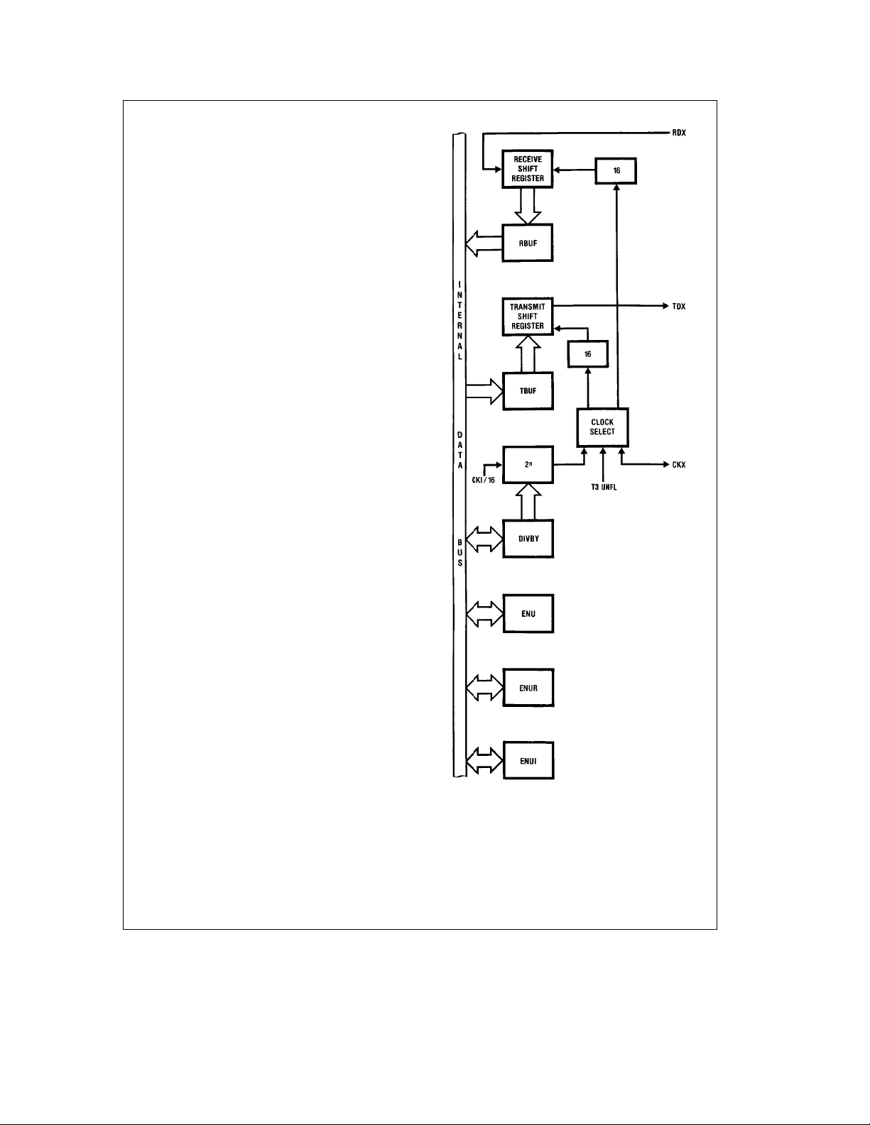
HPC167064 UART
The HPC167064 contains a software programmable UART.
The UART (see
ter, a receiver shift register and five addressable registers,
as follows: a transmit buffer register (TBUF), a receiver buffer register (RBUF), a UART control and status register
(ENU), a UART receive control and status register (ENUR)
and a UART interrupt and clock source register (ENUI). The
ENU register contains flags for transmit and receive functions; this register also determines the length of the data
frame (8 or 9 bits) and the value of the ninth bit in transmission. The ENUR register flags framing and data overrun errors while the UART is receiving. Other functions of the
ENUR register include saving the ninth bit received in the
data frame and enabling or disabling the UART’s Attention
Mode of operation. The determination of an internal or external clock source is done by the ENUI register, as well as
selecting the number of stop bits and enabling or disabling
transmit and receive interrupts.
The baud rate clock for the Receiver and Transmitter can
be selected for either an internal or external source using
two bits in the ENUI register. The internal baud rate is programmed by the DIVBY register. The baud rate may be selected from a range of 8 Hz to 128 kHz in binary steps or T3
underflow. By selecting a 9.83 MHz crystal, all standard
baud rates from 75 baud to 38.4 kBaud can be generated.
The external baud clock source comes from the CKX pin.
The Transmitter and Receiver can be run at different rates
by selecting one to operate from the internal clock and the
other from an external source.
The HPC167064 UART supports two data formats. The first
format for data transmission consists of one start bit, eight
data bits and one or two stop bits. The second data format
for transmission consists of one start bit, nine data bits, and
one or two stop bits. Receiving formats differ from transmission only in that the Receiver always requires only one stop
bit in a data frame.
Figure 26
) consists of a transmit shift regis-
UART Wake-Up Mode
The HPC167064 UART features a Wake-Up Mode of operation. This mode of operation enables the HPC167064 to be
networked with other processors. Typically in such environments, the messages consist of addresses and actual data.
Addresses are specified by having the ninth bit in the data
frame set to 1. Data in the message is specified by having
the ninth bit in the data frame reset to 0.
The UART monitors the communication stream looking for
addresses. When the data word with the ninth bit set is
received, the UART signals the HPC167064 with an interrupt. The processor then examines the content of the receiver buffer to decide whether it has been addressed and
whether to accept subsequent data.
TL/DD/11046– 34
FIGURE 26. UART Block Diagram
23
Page 24
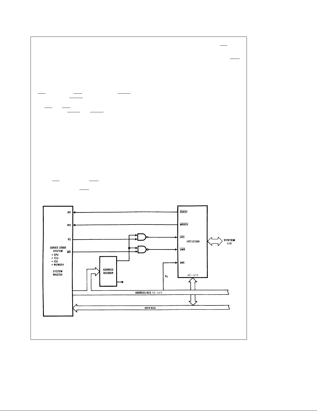
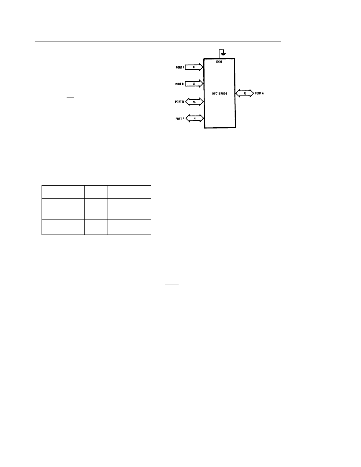
Universal Peripheral Interface
The Universal Peripheral Interface (UPI) allows the
HPC167064 to be used as an intelligent peripheral to another processor. The UPI could thus be used to tightly link two
HPC167064’s and set up systems with very high data exchange rates. Another area of application could be where a
HPC167064 is programmed as an intelligent peripheral to a
host system such as the Series 32000
Figure 27
intelligent peripheral for a Series 32000-based application.
The interface consists of a Data Bus (port A), a Read Strobe
(URD
a Write Ready Line (WRRDY
The data bus can be either eight or sixteen bits wide.
The URD
HPC167064. The RDRDY
used to interrupt the host processor.
The UPI contains an Input Buffer (IBUF), an Output Buffer
(OBUF) and a Control Register (UPIC). In the UPI mode,
Port A on the HPC167064 is the data bus. UPI can only be
used if the HPC167064 is in the Single-Chip mode.
illustrates how a HPC167064 could be used as an
), a Write Strobe (UWR), a Read Ready Line (RDRDY),
) and one Address Input (UA0).
and UWR inputs may be used to interrupt the
and WRRDY outputs may be
microprocessor.
É
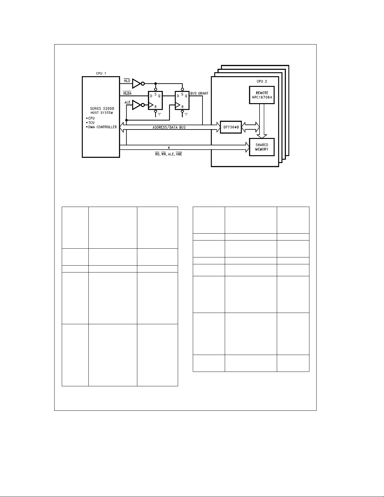
Shared Memory Support
Shared memory access provides a rapid technique to exchange data. It is effective when data is moved from a peripheral to memory or when data is moved between blocks
of memory. A related area where shared memory access
proves effective is in multiprocessing applications where
two CPUs share a common memory block. The HPC167064
supports shared memory access with two pins. The pins are
the RDY/HLD
can software select either the Hold or Ready function by the
state of a control bit. The HLDA
Port B.
input pin and the HLDA output pin. The user
output is multiplexed onto
The host uses DMA to interface with the HPC167064. The
host initiates a data transfer by activating the HLD
the HPC167064. In response, the HPC167064 places its
system bus in a TRI-STATE Mode, freeing it for use by the
host. The host waits for the acknowledge signal (HLDA
from the HPC167064 indicating that the sytem bus is free.
On receiving the acknowledge, the host can rapidly transfer
data into, or out of, the shared memory by using a conventional DMA controller. Upon completion of the message
transfer, the host removes the HOLD request and the
HPC167064 resumes normal operations.
To insure proper operation, the interface logic shown is recommended as the means for enabling and disabling the user’s bus.
Figure 28
memory interface between the HPC167064 and a Series
32000 system.
illustrates an application of the shared
input of
Memory
The HPC167064 has been designed to offer flexibility in
memory usage. A total address space of 64 kbytes can be
addressed with 8 kbytes of EPROM and 512 bytes of RAM
available on the chip itself. The EPROM may contain program instructions, constants or data. The EPROM and RAM
share the same address space allowing instructions to be
executed out of RAM.
Program memory addressing is accomplished by the 16-bit
program counter on a byte basis. Memory can be addressed
directly by instructions or indirectly through the B, X and SP
registers. Memory can be addressed as words or bytes.
Words are always addressed on even-byte boundaries. The
HPC167064 uses memory-mapped organization to support
registers, I/O and on-chip peripheral functions.
The HPC167064 memory address space extends to
64 kbytes and registers and I/O are mapped as shown in
Table III and Table IV.
)
FIGURE 27. HPC167064 as a Peripheral (UPI Interface to Series 32000 Application)
24
TL/DD/11046– 35
Page 25
Shared Memory Support (Continued)
FIGURE 28. Shared Memory Application (HPC167064 Interface to Series 32000 System)
Design Considerations
TABLE III. Memory Map of HPC167064 Emulating an HPC16064
FFFF:FFF0 Interrupt Vectors
FFEF:FFD0 JSRP Vectors
FFCF:FFCE
: : On-Chip ROM
C001:C000
BFFF:BFFE
::
0301:0300
02FF:02FE
: : On-Chip RAM User RAM
01C1:01C0
0195:0194 WATCHDOG Register WATCHDOG Logic
0192 T0CON Register
0191:0190 TMMODE Register
018F:018 DIVBY Register
018D:018C T3 Timer
018B:018A R3 Register
0189:0188 T2 Timer
0187:0186 R2 Register
0185:0184 I2CR Register/ R1
0183:0182 I3CR Register/ T1
0181:0180 I4CR Register
015E:015F EICR
015C EICON
0153:0152 Port P Register
0151:0150 PWMODE Register
014F:014E R7 Register
014D:014C T7 Timer
014B:014A R6 Register Timer Block T4:T7
0149:0148 T6 Timer
0147:0146 R5 Register
0145:0144 T5 Timer
0143:0142 R4 Register
0141:0140 T4 Timer
(
External Expansion
Memory
(
(
User Memory
Timer Block T0:T3
TL/DD/11046– 36
0128 ENUR Register
0126 TBUF Register
0124 RBUF Register UART
0122 ENUI Register
0120 ENU Register
0104 Port D Input Register
00F5:00F4 BFUN Register
00F3:00F2 DIR B Register
00F1:00F0 DIR A Register/IBUF
00E6 UPIC Register UPI Control
00E3:00E2 Port B
00E1:00E0 Port A/OBUF
00DE Reserved
00DD:00DC HALT Enable Register
00D8 Port I Input Register
00D6 SIO Register
00D4 IRCD Register
00D2 IRPD Register
00D0 ENIR Register
00CF:00CE X Register
00CD:00CC B Register
00CB:00CA K Register
00C9:00C8 A Register HPC Core
00C7:00C6 PC Register Registers
00C5:00C4 SP Register
00C3:00C2 Reserved
00C0 PSW Register
00BF:00BE
::
0001:0000
On-Chip
RAM
PortsA&B
Control
PortsA&B
Port Control
& Interrupt
Control
Registers
User RAM
25
Page 26

Design Considerations (Continued)
TABLE IV. Memory Map of HPC167064 Emulating an HPC16083
FFFF:FFF0 Interrupt Vectors
FFEF:FFD0 JSRP Vectors
FFCF:FFCE
: : On-Chip EPROM
E001:E000
DFFF:DFFE External Expansion
: : Memory
0201:0200 (
01FF:01FE
: : On-Chip RAM User RAM
01C1:01C0
0195:0194 WATCHDOG Register WATCHDOG Logic
0192 T0CON Register
0191:0190 TMMODE Register
018F:018E DIVBY Register
018D:018C T3 Timer
018B:018A R3 Register
0189:0188 T2 Timer
0187:0186 R2 Register
0185:0184 I2CR Register/R1
0183:0182 I3CR Register/T1
0181:0180 I4CR Register
015E:015F EICR
015C EICON
0153:0152 Port P Register
0151:0150 PWMODE Register
014F:014E R7 Register
014D:014C T7 Timer
014B:014A R6 Register
0149:0148 T6 Timer
0147:0146 R5 Register
0145:0144 T5 Timer
0143:0142 R4 Register
0141:0140 T4 Timer
( User Memory
(
Timer Block T0:T3
Timer Block T4:T7
0128 ENUR Register
0126 TBUF Register
0124 RBUF Register UART
0122 ENUI Register
0120 ENU Register
0104 Port D Input Register
00F5:00F4 BFUN Register
00F3:00F2 DIR B Register
00F1:00F0 DIR A Register /IBUF
00E6 UPIC Register UPI Control
00E3:00E2 Port B
00E1:00E0 Port A/OBUF
00DE Reserved
00DD:00DC HALT Enable Register
00D8 Port I Input Register
00D6 SIO Register
00D4 IRCD Register
00D2 IRPD Register
00D0 ENIR Register
00CF:00CE X Register
00CD:00CC B Register
00CB:00CA K Register
00C9:00C8 A Register HPC Core
00C7:00C6 PC Register Registers
00C5:00C4 SP Register
00C3:00C2 Reserved
00C0 PSW Register
00BF:00BE
::
0001:0000
On-Chip
RAM
PortsA&B
Control
PortsA&B
Port Control
& Interrupt
Control
Registers
User RAM
26
Page 27
Design Considerations (Continued)
Designs using the HPC family of 16-bit high speed CMOS
microcontrollers need to follow some general guidelines on
usage and board layout.
Floating inputs are a frequently overlooked problem. CMOS
inputs have extremely high impedance and, if left open, can
float to any voltage. You should thus tie unused inputs to
V
or ground, either through a resistor or directly. Unlike
CC
the inputs, unused output should be left floating to allow the
output to switch without drawing any DC current.
To reduce voltage transients, keep the supply line’s parasitic inductances as low as possible by reducing trace lengths,
using wide traces, ground planes, and by decoupling the
supply with bypass capacitors. In order to prevent additional
voltage spiking, this local bypass capacitor must exhibit low
inductive reactance. You should therefore use high frequency ceramic capacitors and place them very near the IC to
minimize wiring inductance.
X
Keep VCCbus routing short. When using double sided or
multilayer circuit boards, use ground plane techniques.
X
Keep ground lines short, and on PC boards make them as
wide as possible, even if trace width varies. Use separate
ground traces to supply high current devices such as relay and transmission line drivers.
X
In systems mixing linear and logic functions and where
supply noise is critical to the analog components’ performance, provide separate supply buses or even separate supplies.
X
If you use local regulators, bypass their inputs with a tantalum capacitor of at least 1 mF and bypass their outputs
with a 10 mFto50mF tantalum or aluminum electrolytic
capacitor.
X
If the system uses a centralized regulated power supply,
usea10mF to 20F tantalum electrolytic capacitor or a
50 mFto100mF aluminum electrolytic capacitor to de-
couple the V
X
Provide localized decoupling. For random logic, a rule of
thumb dictates approximately 10 nF (spaced within
12 cm) per every two to five packages, and 100 nF for
every 10 packages. You can group these capacitances,
but it’s more effective to distribute them among the ICs. If
the design has a fair amount of synchronous logic with
outputs that tend to switch simultaneously, additional decoupling might be advisable. Octal flip-flop and buffers in
bus-oriented circuits might also require more decoupling.
Note that wire-wrapped circuits can require more decoupling than ground plane or multilayer PC boards.
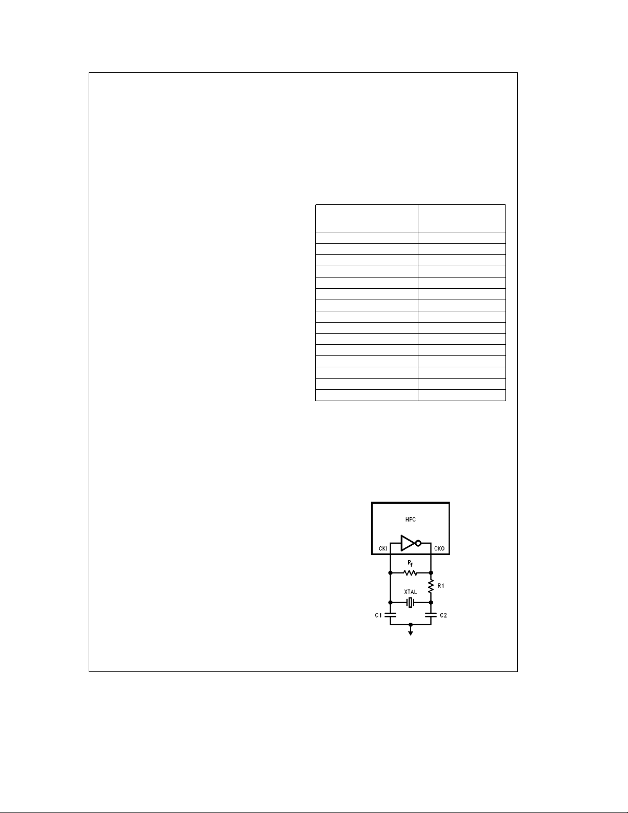
A recommended crystal oscillator circuit to be used with the
HPC is shown in
component values. The recommended values given in
Table V have yielded consistent results and are made to
match a crystal with a 20 pF load capacitance, with some
small allowance for layout capacitance.
A recommended layout for the oscillator network should be
as close to the processor as physically possible, entirely
within 1
×
long PC traces, as well as interference from other components, and reduce trace capacitance. The layout contains a
large ground plane either on the top or bottom surface of
the board to provide signal shielding, and a convenient location to ground both the HPC, and the case of the crystal.
bus connected to the circuit board.
CC
Figure 29
. See table for recommended
distance. This is to reduce lead inductance from
It is very critical to have an extremely clean power supply for
the HPC crystal oscillator. Ideally one would like a V
ground plane that provide low inductance power lines to the
CC
and
chip. The power planes in the PC board should be decoupled with three decoupling capacitors as close to the chip
as possible. A 1.0 mF, a 0.1F, and a 0.001F dipped mica or
ceramic cap should be mounted as close to the HPC as is
physically possible on the board, using the shortest leads,
or surface mount components. This should provide a stable
power supply, and noiseless ground plane which will vastly
improve the performance of the crystal oscillator network.
TABLE V. HPC Oscillator
XTAL
Frequency R
(MHz)
(X)
1
2 1500
4 1200
6 910
8 750
10 600
12 470
14 390
16 300
18 220
20 180
22 150
24 120
26 100
28 75
30 62
e
R
3.3 MX
F
e
27 pF
C
1
e
33 pF
C
2
XTAL Specifications: The crystal used was an M-TRON Industries MP-1 Series XTAL. ‘‘AT’’ cut, parallel resonant.
e
C
20 pF
L
Series Resistance is
@
25X
25 MHz
@
10 MHz
40X
@
2 MHz
600X
TL/DD/11046– 37
FIGURE 29. Recommended Crystal Circuit
27
Page 28

HPC167064 CPU
The HPC167064 CPU has a 16-bit ALU and six 16-bit registers.
Arithmetic Logic Unit (ALU)
The ALU is 16 bits wide and can do 16-bit add, subtract and
shift or logic AND, OR and exclusive OR in one timing cycle.
The ALU can also output the carry bit to a 1-bit C register.
Accumulator (A) Register
The 16-bit A register is the source and destination register
for most I/O, arithmetic, logic and data memory access operations.
Address (B and X) Registers
The 16-bit B and X registers can be used for indirect addressing. They can automatically count up or down to sequence through data memory.
Boundary (K) Register
The 16-bit K register is used to set limits in repetitive loops
of code as register B sequences through data memory.
Stack Pointer (SP) Register
The 16-bit SP register is the pointer that addresses the
stack. The SP register is incremented by two for each push
or call and decremented by two for each pop or return. The
stack can be placed anywhere in user memory and be as
deep as the available memory permits.
Program (PC) Register
The 16-bit PC register addresses program memory.
Addressing Modes
ADDRESSING MODESÐACCUMULATOR AS
DESTINATION
Register Indirect
This is the ‘‘normal’’ mode of addressing for the
HPC167064 (instructions are single-byte). The operand is
the memory addressed by the B register (or X register for
some instructions).
Direct
The instruction contains an 8-bit or 16-bit address field that
directly points to the memory for the operand.
Indirect
The instruction contains an 8-bit address field. The contents
of the WORD addressed points to the memory for the operand.
Indexed
The instruction contains an 8-bit address field and an 8- or
16-bit displacement field. The contents of the WORD addressed is added to the displacement to get the address of
the operand.
Immediate
The instruction contains an 8-bit or 16-bit immediate field
that is used as the operand.
Register Indirect (Auto Increment and Decrement)
The operand is the memory addressed by the X register.
This mode automatically increments or decrements the X
register (by 1 for bytes and by 2 for words).
Register Indirect (Auto Increment and Decrement) with
Conditional Skip
The operand is the memory addressed by the B register.
This mode automatically increments or decrements the B
register (by 1 for bytes and by 2 for words). The B register is
then compared with the K register. A skip condition is generated if B goes past K.
ADDRESSING MODESÐDIRECT MEMORY AS
DESTINATION
Direct Memory to Direct Memory
The instruction contains two 8- or 16-bit address fields. One
field directly points to the source operand and the other field
directly points to the destination operand.
Immediate to Direct Memory
The instruction contains an 8- or 16-bit address field and an
8- or 16-bit immediate field. The immediate field is the operand and the direct field is the destination.
Double Register Indirect Using the B and X Registers
Used only with Reset, Set and IF bit instructions; a specific
bit within the 64 kbyte address range is addressed using the
B and X registers. The address of a byte of memory is
formed by adding the contents of the B register to the most
significant 13 bits of the X register. The specific bit to be
modified or tested within the byte of memory is selected
using the least significant 3 bits of register X.
HPC Instruction Set Description
Mnemonic Description Action
ARITHMETIC INSTRUCTIONS
ADD Add MAaMemIxMA carryxC
ADC Add with carry MA
ADDS Add short imm8 A
DADC Decimal add with carry MA
SUBC Subtract with carry MA
DSUBC Decimal subtract w/carry MA
MULT Multiply (unsigned) MA*MemI
DIV Divide (unsigned) MA/MemI
DIVD Divide Double Word (unsigned) X & MA/MemIxMA, remxX, 0xK, carryxC
IFEQ If equal Compare MA & MemI, Do next if equal
IFGT If greater than Compare MA & MemI, Do next if MA
AND Logical AND MA and MemI
OR Logical OR MA or MemI
XOR Logical Exclusive-OR MA xor MemI
MEMORY MODIFY INSTRUCTIONS
INC Increment Mema1xMem
DECSZ Decrement, skip if 0 Mem
a
MemIaCMA carryxC
a
imm8xA carryxC
a
MemIaCxMA (Decimal) carryxC
b
MemIaCxMA carryxC
b
MemIaCxMA (Decimal) carryxC
x
MA&X,0xK, 0xC
x
MA, remxX, 0xK, 0xC
x
MA
x
MA
x
MA
b
1xMem, Skip next if Meme0
l
MemI
28
Page 29

HPC Instruction Set Description (Continued)
Mnemonic Description Action
BIT INSTRUCTIONS
SBIT Set bit 1xMem.bit
RBIT Reset bit 0
IFBIT If bit If Mem.bit is true, do next instr.
MEMORY TRANSFER INSTRUCTIONS
LD Load MemIxMA
ST Store to Memory A
X Exchange A
PUSH Push Memory to Stack W
POP Pop Stack to Memory SP
LDS Load A, incr/decr B, Mem(B)xA, Bg1 (or 2)xB,
XS Exchange, incr/decr B, Mem(B)
REGISTER LOAD IMMEDIATE INSTRUCTIONS
LD B Load B immediate immxB
LD K Load K immediate imm
LD X Load X immediate imm
LD BK Load B and K immediate imm
ACCUMULATOR AND C INSTRUCTIONS
CLR A Clear A 0xA
INC A Increment A A
DEC A Decrement A A
COMP A Complement A 1’s complement of A
SWAP A Swap nibbles of A A[15:12
RRC A Rotate A right thru C C
RLC A Rotate A left thru C C
SHR A Shift A right 0xA15x...xA0xC
SHL A Shift A left C
SC Set C 1
RC Reset C 0
IFC IF C Do next if C
IFNC IF not C Do next if C
TRANSFER OF CONTROL INSTRUCTIONS
JSRP Jump subroutine from table PCxW(SP),SPa2xSP
JSR Jump subroutine relative PC
JSRL Jump subroutine long PC
JP Jump relative short PC
JMP Jump relative PC
JMPL Jump relative long PC
JID Jump indirect at PC
JIDW then Mem(PC)
NOP No Operation PC
RET Return SP
RETSK Return then skip next SP
RETI Return from interrupt SP
Note: W is 16-bit word of memory
MA is Accumulator A or direct memory (8-bit or 16-bit)
Mem is 8-bit byte or 16-bit word of memory
MemI is 8-bit or 16-bit memory or 8-bit or 16-bit immediate data
imm is 8-bit or 16-bit immediate data
imm8 is 8-bit immediate data only
For details of memory usage by each instruction, see The HPC User’s Manual.
Load, incr/decr X Mem(X)
Exchange, incr/decr X A
Skip on condition Skip next if B greater/less than K
Skip on condition Skip next if B greater/less than K
a
APC
x
Mem.bit
x
x
Ý
Ý
x
a
b
x
w
w
x
x
W(table
(
A, Xg1 (or 2)xX
Mem
Mem
Mem(X), Xg1 (or 2)xX
W(SP), SPa2xSP
b
2xSP, W(SP)xW
Ý
A, Bg1 (or 2)xB,
x
K
x
X
x
B, immxK
1xA
1xA
]
w
A[11:8
A15x...xA0xC
A15w...wA0wC
A15w...wA0w0
C
C
e
e
Ý
)xPC
x
W(SP),SPa2xSP,PC
Ý
isa1025 tob1023)
x
W(SP),SPa2xSP,PC
a
Ý
x
PC(Ýisa32 tob31)
a
Ý
x
PC(Ýisa257 tob255)
a
Ý
x
PC
a
a
A
1
x
a
1xPC
b
2xSP,W(SP)xPC
b
2xSP,W(SP)xPC, & skip
b
2xSP,W(SP)xPC, interrupt re-enabled
1
0
PC
a
x
A
]
w
A[7:4
PCxPC
]
Ý
a
a
]
A[3:0
Ý
x
PC
Ý
x
PC
29
Page 30

Code Efficiency
One of the most important criteria of a single chip microcontroller is code efficiency. The more efficient the code, the
more features that can be put on a chip. The memory size
on a chip is fixed so if code is not efficient, features may
have to be sacrificed or the programmer may have to buy a
larger, more expensive version of the chip.
The HPC family has been designed to be extremely codeefficient. The HPC looks very good in all the standard coding benchmarks; however, it is not realistic to rely only on
benchmarks. Many large jobs have been programmed onto
the HPC, and the code savings over other popular microcontrollers has been considerable.
Reasons for this saving of code include the following:
SINGLE BYTE INSTRUCTIONS
The majority of instructions on the HPC167064 are singlebyte. There are two especially code-saving instructions: JP
is a 1-byte jump. True, it can only jump within a range of plus
or minus 32, but many loops and decisions are often within
a small range of program memory. Most other micros need
2-byte instructions for any short jumps.
JSRP is a 1-byte subroutine call. The user makes a table of
the 16 most frequently called subroutines and these calls
will only take one byte. Most other micros require two and
even three bytes to call a subroutine. The user does not
have to decide which subroutine addresses to put into the
table; the assembler can give this information.
EFFICIENT SUBROUTINE CALLS
The 2-byte JSR instructions can call any subroutine within
plus or minus 1k of program memory.
MULTIFUNCTION INSTRUCTIONS FOR DATA MOVEMENT AND PROGRAM LOOPING
The HPC167064 has single-byte instructions that perform
multiple tasks. For example, the XS instruction will do the
following:
1. Exchange A and memory pointed to by the B register
2. Increment or decrement the B register
3. Compare the B register to the K register
4. Generate a conditional skip if B has passed K
The value of this multipurpose instruction becomes evident
when looping through sequential areas of memory and exiting when the loop is finished.
BIT MANIPULATION INSTRUCTIONS
Any bit of memory, I/O or registers can be set, reset or
tested by the single byte bit instructions. The bits can be
addressed directly or indirectly. Since all registers and I/O
are mapped into the memory, it is very easy to manipulate
specific bits to do efficient control.
DECIMAL ADD AND SUBTRACT
This instruction is needed to interface with the decimal user
world.
It can handle both 16-bit words and 8-bit bytes.
The 16-bit capability saves code since many variables can
be stored as one piece of data and the programmer does
not have to break his data into two bytes. Many applications
store most data in 4-digit variables. The HPC167064 supplies 8-bit byte capability for 2-digit variables and literal variables.
MULTIPLY AND DIVIDE INSTRUCTIONS
The HPC167064 has 16-bit multiply, 16-bit by 16-bit divide,
and 32-bit by 16-bit divide instructions. This saves both
code and time. Multiply and divide can use immediate data
or data from memory. The ability to multiply and divide by
immediate data saves code since this function is often
needed for scaling, base conversion, computing indexes of
arrays, etc.
Development Support
The HPC167064 acts as a stand alone emulator for either
the HPC16083 or the HPC16064. No separate development
tool is thus provided to support this emulator device. The
user will use either the HPC16083 or the HPC16064 (depending on which device is in use) development tools to
develop and debug the application hardware and software
in their target as normally done for the non-emulator HPC
devices. The application software can then be programmed
in the on-chip EPROM and the HPC167064 can then be
plugged in the target system to run the application like a
regular masked ROM device. The HPC167064 can be programmed using a DATA I/O UNISITE with pinsite module.
To support the security feature of the HPC167064, a software switch is provided with the linker (under PROMHPC)
which will generate an encrypted hex file for the user. The
purpose is to be able to compare this software generated
encrypted data with the encrypted data produced by the
actual chip to provide a way to verify on-chip EPROM code
after security has been enabled. For details of how to generate encrypted data and all other HPC167064 features, refer
to the Appendix K of the HPC Family User’s Manual.
30
Page 31
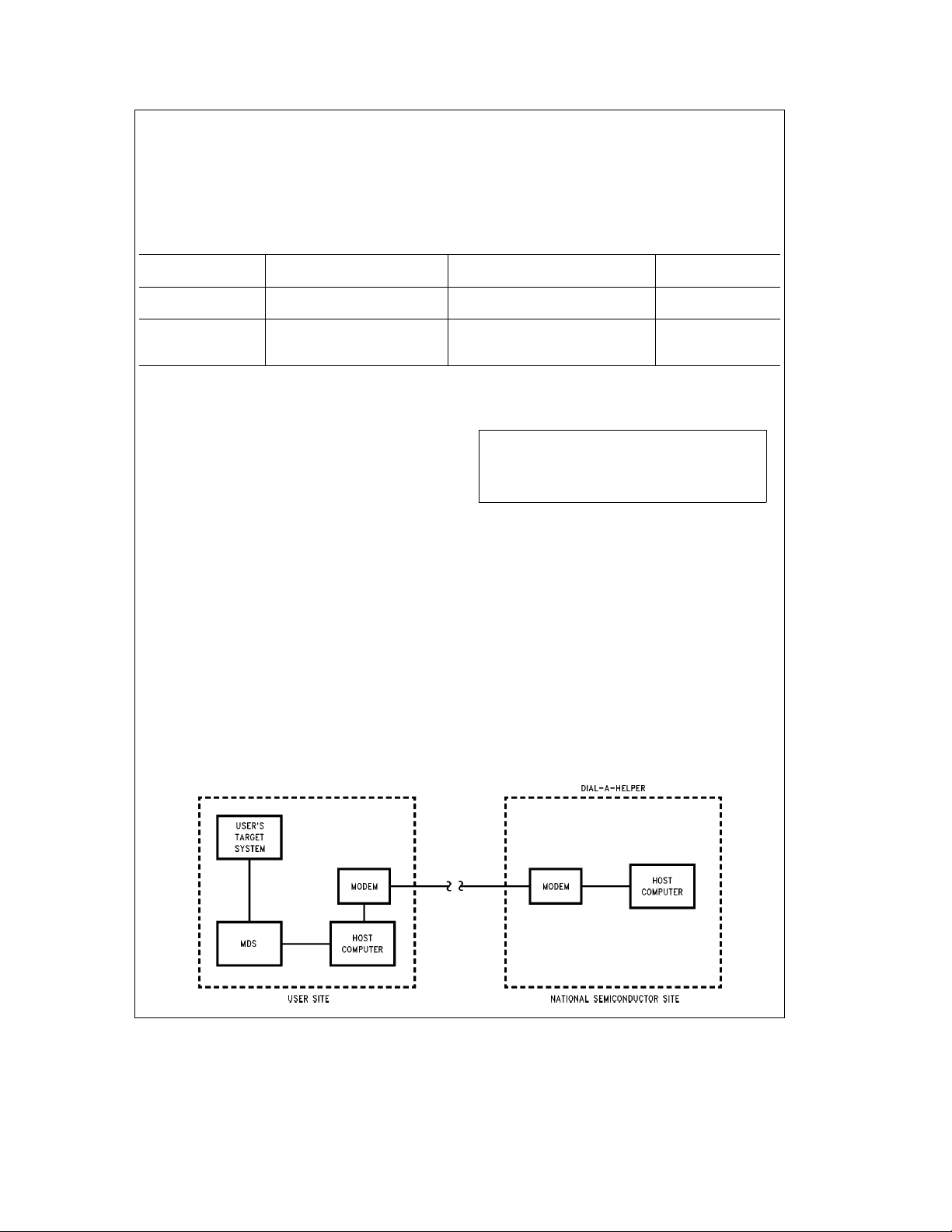
Development Support (Continued)
PROGRAMMING SUPPORT
The HPC167064 EPROM array can be programmed using a
DATA I/O Unisite model with a pinsite module. No adaptor
board is required with the DATA I/O programmer. Programming of the configuration bytes and security bits is described in the HPC Family User’s Manual.
Development Tools Selection Table
Order
Number Number
HPC-DEV-IBMA Assembler/Linker/Librarian HPC Assembler/Linker/Librarian 424410836-001
HPC-DEV-IBMC C Compiler HPC C Compiler User’s Manual 424410883-001
Description Includes
Package for IBM PC/AT User’s Manual
Assembler/Linker/Librarian HPC Assembler/Linker/Librarian 424410836-001
Package for IBM PC/AT User’s Manual
HOW TO ORDER
To order a complete development package, select the section for the microcontroller to be developed and order the
parts listed.
Manual
DIAL-A-HELPER
Dial-A-Helper is a service provided by the Microcontroller
Applications group. Dial-A-Helper is an Electronic Bulletin
Board Information system and, additionally, provides the capability of remotely accessing the development system at a
customer site.
INFORMATION SYSTEM
The Dial-A-Helper system provides access to an automated
information storage and retrieval system that may be accessed over standard dial-up telephone lines 24 hours a
day. The system capabilities include a MESSAGE SECTION
(electronic mail) for communications to and from the Microcontroller Applications Group and a FILE SECTION which
consists of several file areas where valuable application
software and utilities can be found. The minimum requirement for accessing Dial-A-Helper is a Hayes compatible modem.
Voice: (408) 721-5582
Modem: (408) 739-1162
Baud: 300 or 1200 baud
Set-Up: Length: 8-bit
Operation: 24 hrs, 7 Days
If the user has a PC with a communications package then
files from the FILE SECTION can be downloaded to disk for
later use.
Order P/N: MDS-DIAL-A-HLP
Information System Package Contains:
Dial-A-Helper Users Manual
Public Domain Communications Software
FACTORY APPLICATIONS SUPPORT
Dial-A-Helper also provides immediate factory applications
support. If a user is having difficulty in operating a MDS,
messages can be left on our electronic bulletin board, which
we will respond to.
Parity: None
Stop Bit: 1
TL/DD/11046– 38
31
Page 32
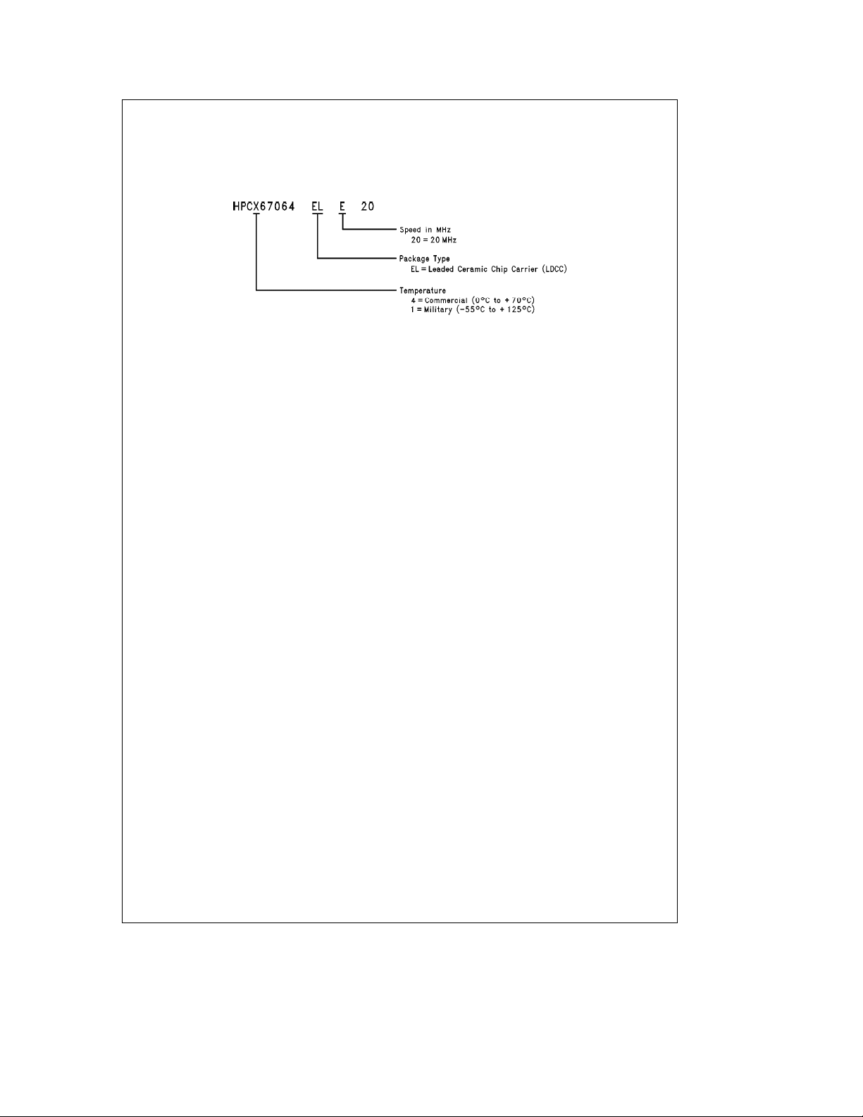
Part Selection
The HPC family includes devices with many different options and configurations to meet various application needs. The
number HPC167064 has been generically used throughout this datasheet to represent the whole family of parts. The
following chart explains how to order various options available when ordering HPC family members.
Note: All options may not currently be available.
TL/DD/11046– 39
Examples:
HPC467064/EL20Ð16k EPROM, Commercial temperature (0§Ctoa70§C), LDCC
HPC167064/EL20Ð16k EPROM Military temperature (b55§Ctoa125§C), LDCC (to be used for automotive
temperature range also)
Socket Selection
Suggested sockets and extractor tool:
Socket
Ý
Amp PLCC
*YAMAICHI 1C51-0684-390
1C120-0684-204
ENPLAS PLCC-68-1.27-02
Extractors Tool
*A shim must be used in conjunction with this socket to ensure proper contacts. For details of the shim and how to obtain it, contact factory applications group
at (408) 721-5582.
Ý
Amp 821566-1
Ý
821574-1
6141749
32
Page 33

33
Page 34
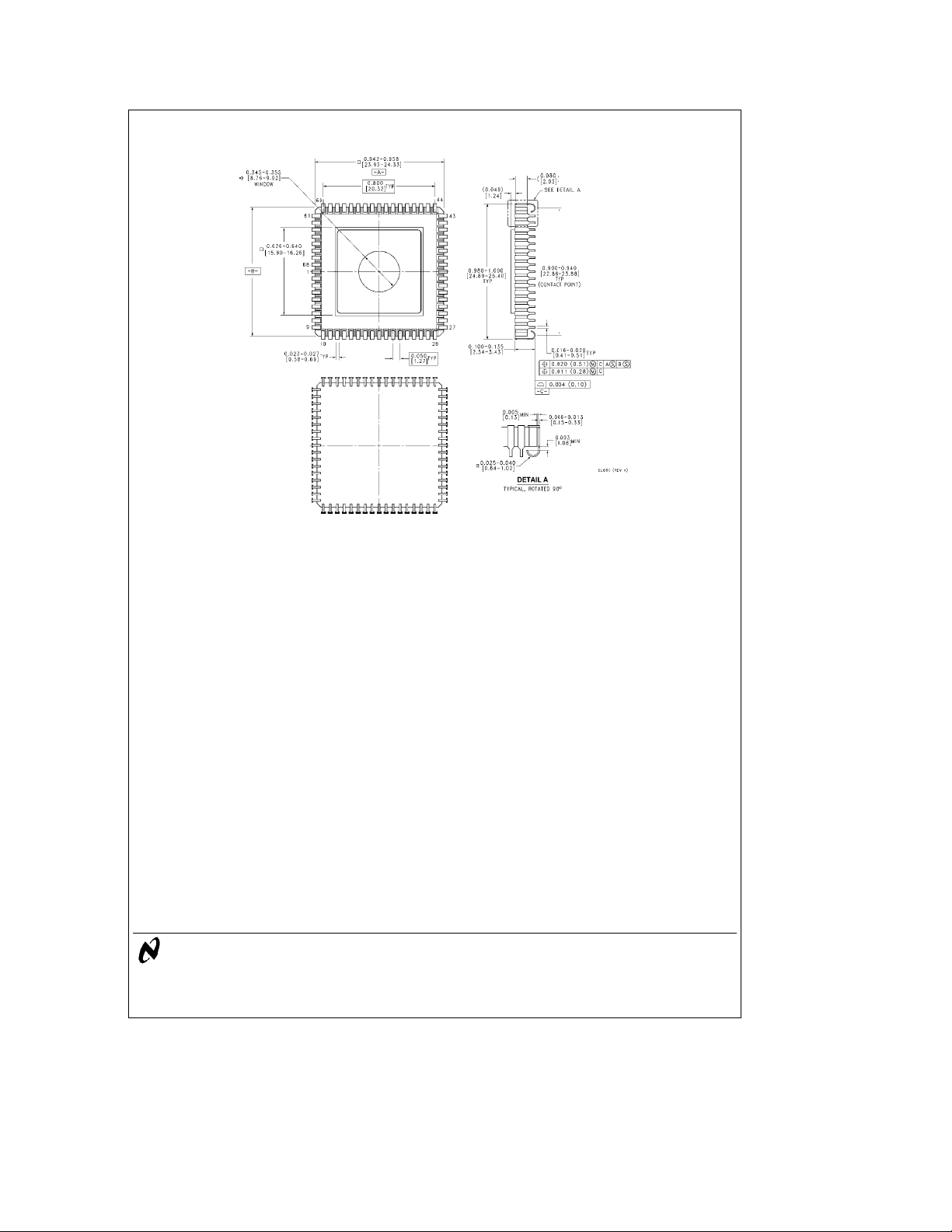
Physical Dimensions inches (millimeters)
with a 16k UV Erasable CMOS EPROM
Order Number HPC167064EL or HPC467064EL
Leaded EPROM Chip Carrier (EL)
NS Package Number EL68C
HPC167064/HPC467064 High-Performance microController
LIFE SUPPORT POLICY
NATIONAL’S PRODUCTS ARE NOT AUTHORIZED FOR USE AS CRITICAL COMPONENTS IN LIFE SUPPORT
DEVICES OR SYSTEMS WITHOUT THE EXPRESS WRITTEN APPROVAL OF THE PRESIDENT OF NATIONAL
SEMICONDUCTOR CORPORATION. As used herein:
1. Life support devices or systems are devices or 2. A critical component is any component of a life
systems which, (a) are intended for surgical implant support device or system whose failure to perform can
into the body, or (b) support or sustain life, and whose be reasonably expected to cause the failure of the life
failure to perform, when properly used in accordance support device or system, or to affect its safety or
with instructions for use provided in the labeling, can effectiveness.
be reasonably expected to result in a significant injury
to the user.
National Semiconductor National Semiconductor National Semiconductor National Semiconductor
Corporation Europe Hong Kong Ltd. Japan Ltd.
1111 West Bardin Road Fax: (
Arlington, TX 76017 Email: cnjwge@tevm2.nsc.com Ocean Centre, 5 Canton Rd. Fax: 81-043-299-2408
Tel: 1(800) 272-9959 Deutsch Tel: (
Fax: 1(800) 737-7018 English Tel: (
National does not assume any responsibility for use of any circuitry described, no circuit patent licenses are implied and National reserves the right at any time without notice to change said circuitry and specifications.
Fran3ais Tel: (
Italiano Tel: (
a
49) 0-180-530 85 86 13th Floor, Straight Block, Tel: 81-043-299-2309
a
49) 0-180-530 85 85 Tsimshatsui, Kowloon
a
49) 0-180-532 78 32 Hong Kong
a
49) 0-180-532 93 58 Tel: (852) 2737-1600
a
49) 0-180-534 16 80 Fax: (852) 2736-9960
 Loading...