

Page 1

T
VXI
GPIB-VXI/C User Manual
GPIB-VXI/C User Manual
May 2002 Edition
Part Number 370556A-01
Page 2

Support
Worldwide Technical Support and Product Information
ni.com
National Instruments Corporate Headquarters
11500 North Mopac Expressway Austin, Texas 78759-3504 USA Tel: 512 683 0100
Worldwide Offices
Australia0398795166, Austria06624579900, Belgium 02 757 00 20, Brazil 011 3262 3599,
Canada (Calgary) 403 274 9391, Canada (Montreal) 514 288 5722, Canada (Ottawa) 613 233 5949,
Canada (Québec) 514 694 8521, Canada (Toronto) 905 785 0085, China (Shanghai) 021 6555 7838,
China (ShenZhen) 0755 3904939, Czech Republic 02 2423 5774, Denmark 45 76 26 00, Finland 09 725 725 11,
France 01 48 14 24 24, Germany 089 741 31 30, Greece 30 1 42 96 427, Hong Kong 2645 3186,
India 91 80 4190000, Israel 03 6393737, Italy 02 413091, Japan 03 5472 2970, Korea 02 3451 3400,
Malaysia 603 9596711, Mexico 001 800 010 0793, Netherlands 0348 433466, New Zealand 09 914 0488,
Norway 32 27 73 00, Poland 0 22 3390 150, Portugal 351 210 311 210, Russia 095 238 7139,
Singapore 6 2265886, Slovenia 386 3 425 4200, South Africa 11 805 8197, Spain 91 640 0085,
Sweden 08 587 895 00, Switzerland 056 200 51 51, Taiwan 02 2528 7227, United Kingdom 01635 523545
For further support information, see the Technical Support and Professional Services appendix. To comment on
the documentation, send email to techpubs@ni.com.
© 2002 National Instruments Corporation. All rights reserved.
Page 3

Important Information
Warranty
The GPIB-VXI/C is warranted against defects in materials and workmanship for a period of one year from the date of shipment, as evidenced
by receipts or other documentation. National Instruments will, at its option, repair or replace equipment that proves to be defective during the
warranty period. This warranty includes parts and labor.
The media on which you receive National Instruments software are warranted not to fail to execute programming instructions, due to defects
in materials and workmanship, for a period of 90 days from date of shipment, as evidenced by receipts or other documentation. National
Instruments will, at its option, repair or replace software media that do not execute programming instructions if National Instruments receives
notice of such defects during the warranty period. National Instruments does not warrant that the operation of the software shall be
uninterrupted or error free.
A Return Material Authorization (RMA) number must be obtained from the factory and clearly marked on the outside of the package before
any equipment will be accepted for warranty work. National Instruments will pay the shipping costs of returning to the owner parts which are
covered by warranty.
National Instruments believes that the information in this document is accurate. The document has been carefully reviewed for technical
accuracy. In the event that technical or typographical errors exist, National Instruments reserves the right to make changes to subsequent
editions of this document without prior notice to holders of this edition. The reader should consult National Instruments if errors are suspected.
In no event shall National Instruments be liable for any damages arising out of or related to this document or the information contained in it.
XCEPT AS SPECIFIED HEREIN, NATIONAL INSTRUMENTS MAKES NO WARRANTIES, EXPRESS OR IMPLIED, AND SPECIFICALLY DISCLAIMS ANY WAR RANTY OF
E
MERCHANTABILITY OR FITNESS FOR A PARTICULAR PURPOSE . CUSTOMER’S RIGHT TO RECOVER DAMAGES CAUSED BY FAULT OR NEGLIGENCE ON THE PART OF
N
ATIONAL INSTRUMENTS SHALL BE LIMITED TO THE AMOUNT THERETOFORE PAID BY THE CUSTOMER. NATIONAL INSTRUMENTS WILL NOT BE LIABLE FOR
DAMAGES RESULTING FROM LOSS OF DATA, PROFITS, USE OF PRODUCTS, OR INCIDENTAL OR CONSEQUENTIAL DAMAGES, EVEN IF ADVISED OF THE POSS IBILITY
THEREOF. This limitation of the liability of National Instruments will apply regardless of the form of action, whether in contract or tort, including
negligence. Any action against National Instruments must be brought within one year after the cause of action accrues. National Instruments
shall not be liable for any delay in performance due to causes beyond its reasonable control. The warranty provided herein does not cover
damages, defects, malfunctions, or service failures caused by owner’s failure to follow the National Instruments installation, operation, or
maintenance instructions; owner’s modification of the product; owner’s abuse, misuse, or negligent acts; and power failure or surges, fire,
flood, accident, actions of third parties, or other events outside reasonable control.
Copyright
Under the copyright laws, this publication may not be reproduced or transmitted in any form, electronic or mechanical, including photocopying,
recording, storing in an information retrieval system, or translating, in whole or in part, without the prior written consent of National
Instruments Corporation.
Trademarks
MANTIS™, MIGA™, National Instruments™, NI™, NI-488™, ni.com™, NI-VISA™, TIC™, and TNT4882™ are trademarks of
National Instruments Corporation.
Product and company names mentioned herein are trademarks or trade names of their respective companies.
Patents
For patents covering National Instruments products, refer to the appropriate location: Help»Patents in your software, the patents.txt file
on your CD, or
ni.com/patents.
WARNING REGARDING USE OF NATIONAL INSTRUMENTS PRODUCTS
(1) NATIONAL INSTRUMENTS PRODUCTS ARE NOT DESIGNED WITH COMPONENTS AND TESTING FOR A LEVEL OF
RELIABILITY SUITABLE FOR USE IN OR IN CONNECTION WITH SURGICAL IMPLANTS OR AS CRITICAL COMPONENTS IN
ANY LIFE SUPPORT SYSTEMS WHOSE FAILURE TO PERFORM CAN REASONABLY BE EXPECTED TO CAUSE SIGNIFICANT
INJURY TO A HUMAN.
(2) IN ANY APPLICATION, INCLUDING THE ABOVE, RELIABILITY OF OPERATION OF THE SOFTWARE PRODUCTS CAN BE
IMPAIRED BY ADVERSE FACTORS, INCLUDING BUT NOT LIMITED TO FLUCTUATIONS IN ELECTRICAL POWER SUPPLY,
COMPUTER HARDWARE MALFUNCTIONS, COMPUTER OPERATING SYSTEM SOFTWARE FITNESS, FITNESS OF COMPILERS
AND DEVELOPMENT SOFTWARE USED TO DEVELOP AN APPLICATION, INSTALLATION ERRORS, SOFTWARE AND
HARDWARE COMPATIBILITY PROBLEMS, MALFUNCTIONS OR FAILURES OF ELECTRONIC MONITORING OR CONTROL
DEVICES, TRANSIENT FAILURES OF ELECTRONIC SYSTEMS (HARDWARE AND/OR SOFTWARE), UNANTICIPATED USES OR
MISUSES, OR ERRORS ON THE PART OF THE USER OR APPLICATIONS DESIGNER (ADVERSE FACTORS SUCH AS THESE ARE
HEREAFTER COLLECTIVELY TERMED “SYSTEM FAILURES”). ANY APPLICATION WHERE A SYSTEM FAILURE WOULD
CREATE A RISK OF HARM TO PROPERTY OR PERSONS (INCLUDING THE RISK OF BODILY INJURY AND DEATH) SHOULD
NOT BE RELIANT SOLELY UPON ONE FORM OF ELECTRONIC SYSTEM DUE TO THE RISK OF SYSTEM FAILURE. TO AVOID
DAMAGE, INJURY, OR DEATH, THE USER OR APPLICATION DESIGNER MUST TAKE REASONABLY PRUDENT STEPS TO
PROTECT AGAINST SYSTEM FAILURES, INCLUDING BUT NOT LIMITED TO BACK-UP OR SHUT DOWN MECHANISMS.
BECAUSE EACH END-USER SYSTEM IS CUSTOMIZED AND DIFFERS FROM NATIONAL INSTRUMENTS' TESTING
PLATFORMS AND BECAUSE A USER OR APPLICATION DESIGNER MAY USE NATIONAL INSTRUMENTS PRODUCTS IN
COMBINATION WITH OTHER PRODUCTS IN A MANNER NOT EVALUATED OR CONTEMPLATED BY NATIONAL
INSTRUMENTS, THE USER OR APPLICATION DESIGNER IS ULTIMATELY RESPONSIBLE FOR VERIFYING AND VALIDATING
THE SUITABILITY OF NATIONAL INSTRUMENTS PRODUCTS WHENEVER NATIONAL INSTRUMENTS PRODUCTS ARE
INCORPORATED IN A SYSTEM OR APPLICATION, INCLUDING, WITHOUT LIMITATION, THE APPROPRIATE DESIGN,
PROCESS AND SAFETY LEVEL OF SUCH SYSTEM OR APPLICATION.
Page 4

Compliance
FCC/Canada Radio Frequency Interference Compliance*
Determining FCC Class
The Federal Communications Commission (FCC) has rules to protect wireless communications from interference. The FCC
places digital electronics into two classes. These classes are known as Class A (for use in industrial-commercial locations only)
or Class B (for use in residential or commercial locations). Depending on where it is operated, this product could be subject to
restrictions in the FCC rules. (In Canada, the Department of Communications (DOC), of Industry Canada, regulates wireless
interference in much the same way.)
Digital electronics emit weak signals during normal operation that can affect radio, television, or other wireless products. By
examining the product you purchased, you can determine the FCC Class and therefore which of the two FCC/DOC Warnings
apply in the following sections. (Some products may not be labeled at all for FCC; if so, the reader should then assume these are
Class A devices.)
FCC Class A products only display a simple warning statement of one paragraph in length regarding interference and undesired
operation. Most of our products are FCC Class A. The FCC rules have restrictions regarding the locations where FCC Class A
products can be operated.
FCC Class B products display either a FCC ID code, starting with the letters EXN,
or the FCC Class B compliance mark that appears as shown here on the right.
Consult the FCC Web site at
FCC/DOC Warnings
This equipment generates and uses radio frequency energy and, if not installed and used in strict accordance with the instructions
in this manual and the CE Mark Declaration of Conformity**, may cause interference to radio and television reception.
Classification requirements are the same for the Federal Communications Commission (FCC) and the Canadian Department
of Communications (DOC).
Changes or modifications not expressly approved by National Instruments could void the user’s authority to operate the
equipment under the FCC Rules.
http://www.fcc.gov for more information.
Class A
Federal Communications Commission
This equipment has been tested and found to comply with the limits for a Class A digital device, pursuant to part 15 of the FCC
Rules. These limits are designed to provide reasonable protection against harmful interference when the equipment is operated
in a commercial environment. This equipment generates, uses, and can radiate radio frequency energy and, if not installed and
used in accordance with the instruction manual, may cause harmful interference to radio communications. Operation of this
equipment in a residential area is likely to cause harmful interference in which case the user will be required to correct
the interference at his own expense.
Canadian Department of Communications
This Class A digital apparatus meets all requirements of the Canadian Interference-Causing Equipment Regulations.
Cet appareil numérique de la classe A respecte toutes les exigences du Règlement sur le matériel brouilleur du Canada.
Class B
Federal Communications Commission
This equipment has been tested and found to comply with the limits for a Class B digital device, pursuant to part 15 of the
FCC Rules. These limits are designed to provide reasonable protection against harmful interference in a residential installation.
This equipment generates, uses, and can radiate radio frequency energy and, if not installed and used in accordance with the
instructions, may cause harmful interference to radio communications. However, there is no guarantee that interference will not
occur in a particular installation. If this equipment does cause harmful interference to radio or television reception, which can
be determined by turning the equipment off and on, the user is encouraged to try to correct the interference by one or more of
the following measures:
• Reorient or relocate the receiving antenna.
• Increase the separation between the equipment and receiver.
• Connect the equipment into an outlet on a circuit different from that to which the receiver is connected.
• Consult the dealer or an experienced radio/TV technician for help.
Page 5

Canadian Department of Communications
This Class B digital apparatus meets all requirements of the Canadian Interference-Causing Equipment Regulations.
Cet appareil numérique de la classe B respecte toutes les exigences du Règlement sur le matériel brouilleur du Canada.
Compliance to EU Directives
Readers in the European Union (EU) must refer to the Manufacturer’s Declaration of Conformity (DoC) for information**
pertaining to the CE Mark compliance scheme. The Manufacturer includes a DoC for most every hardware product except for
those bought for OEMs, if also available from an original manufacturer that also markets in the EU, or where compliance is not
required as for electrically benign apparatus or cables.
To obtain the DoC for this product, click Declaration of Conformity at
by product family. Select the appropriate product family, followed by your product, and a link to the DoC appears in Adobe
Acrobat format. Click the Acrobat icon to download or read the DoC.
* Certain exemptions may apply in the USA, see FCC Rules §15.103 Exempted devices, and §15.105(c). Also available in
sections of CFR 47.
** The CE Mark Declaration of Conformity will contain important supplementary information and instructions for the user or
installer.
ni.com/hardref.nsf/. This Web site lists the DoCs
Page 6

Contents
About This Manual
Conventions ...................................................................................................................xiii
Related Documentation..................................................................................................xiv
Chapter 1
General Description
Overview........................................................................................................................1-1
What Your Kit Should Contain .....................................................................................1-1
Optional Equipment.......................................................................................................1-1
Unpacking......................................................................................................................1-2
VXIbus Characteristics ..................................................................................................1-2
GPIB Characteristics......................................................................................................1-2
Local Command Set Overview......................................................................................1-3
Code Instruments ...........................................................................................................1-4
Front Panel Features ......................................................................................................1-5
Chapter 2
Configuration and Startup Procedures
System Configuration ....................................................................................................2-1
GPIB-VXI/C Configuration...........................................................................................2-2
Setting the Logical Address, GPIB Primary Address,
and Servant Area Size...................................................................................2-4
Verifying the Installed RAM Size...................................................................2-4
Setting the Shared Memory Size .....................................................................2-5
Setting the Reset Operation .............................................................................2-6
Setting the VXIbus Requester Level ...............................................................2-6
Setting the VXI Interrupt Handler Levels .......................................................2-7
External Input Termination .............................................................................2-8
EPROM Configuration....................................................................................2-9
Discrete Fault Indicator Configuration............................................................2-10
Address Modifier Configuration .....................................................................2-11
GPIB-VXI/C Startup Mode Configuration .....................................................2-12
488-VXI Runtime System Operation ............................................................................2-13
System Startup Message Printing....................................................................2-14
Slot 0 Resource Manager Configuration .........................................................2-14
Slot 0 Resource Manager Operation .................................................2-15
Front Panel LED Indications for RM Operation...............................2-15
Self-Test Operation ...........................................................................2-16
© National Instruments Corporation vii GPIB-VXI/C User Manual
Page 7

Contents
Non-Slot 0 Resource Manager Configuration ................................................ 2-20
Non-Slot 0 Message-Based Device Configuration
(Non-Resource Manager)............................................................................. 2-21
Slot 0 Message-Based Device Configuration ................................................. 2-23
Chapter 3
Local Command Set
Command Set Access .................................................................................................... 3-2
Command Syntax .......................................................................................................... 3-2
Command Line Termination ......................................................................................... 3-3
Command and Query Responses................................................................................... 3-3
Command Response Format.......................................................................................... 3-4
Query Response Format ................................................................................................ 3-4
Error Reporting.............................................................................................................. 3-4
The Help Query ............................................................................................................. 3-4
Help? ............................................................................................................... 3-5
General Configuration Commands and Queries............................................................ 3-6
CONF .............................................................................................................. 3-7
ConsoleEna ..................................................................................................... 3-7
ConsMode ....................................................................................................... 3-8
DIAG............................................................................................................... 3-8
DPram?............................................................................................................ 3-9
NVconf? ..........................................................................................................3-10
OBram? ........................................................................................................... 3-11
ProgMode........................................................................................................ 3-12
WordSerEna .................................................................................................... 3-13
RM Information Queries ............................................................................................... 3-14
A24MemMap? ................................................................................................ 3-15
A32MemMap? ................................................................................................ 3-16
Cmdr?.............................................................................................................. 3-17
CmdrTable?..................................................................................................... 3-18
Laddrs?............................................................................................................ 3-19
NumLaddrs?.................................................................................................... 3-19
RM Operation ................................................................................... 2-16
Static Configuration Operation.........................................................2-18
Dynamic Configuration Operation ................................................... 2-18
GPIB Address Assignment............................................................... 2-19
System Configuration Table............................................................. 2-20
Non-Slot 0 Resource Manager Operation......................................... 2-21
Non-Slot 0 Message-Based Device Operation ................................. 2-22
Front Panel LED Indications for Message-Based
Device Operation ........................................................................... 2-22
Slot 0 Message-Based Device Operation ......................................... 2-24
GPIB-VXI/C User Manual viii ni.com
Page 8

Contents
RmEntry?.........................................................................................................3-20
Srvnts? .............................................................................................................3-22
StatusState?......................................................................................................3-23
Dynamic Configuration Commands and Queries..........................................................3-24
DCBNOSend ...................................................................................................3-25
DCGrantDev....................................................................................................3-25
DCSystem? ......................................................................................................3-26
Dynamic Reconfiguration Queries ................................................................................3-27
Broadcast? .......................................................................................................3-28
GrantDev?........................................................................................................3-31
RelSrvnt? .........................................................................................................3-32
VXI-Defined Common ASCII System Commands.......................................................3-33
DCON? ............................................................................................................3-34
DINF? ..............................................................................................................3-36
DLAD? ............................................................................................................3-38
DNUM? ...........................................................................................................3-39
DRES? .............................................................................................................3-40
RREG?.............................................................................................................3-41
WREG .............................................................................................................3-42
GPIB Address Configuration Commands and Queries .................................................3-43
LaSaddr............................................................................................................3-44
LaSaddr?..........................................................................................................3-45
Primary? ..........................................................................................................3-46
SaddrLa?..........................................................................................................3-47
Saddrs? ............................................................................................................3-48
SaDisCon.........................................................................................................3-48
VXIbus Interrupt Handler Configuration Commands and Queries ...............................3-49
AllHandlers?....................................................................................................3-50
AssgnHndlr......................................................................................................3-51
HandlerLine? ...................................................................................................3-52
RdHandlers? ....................................................................................................3-53
IEEE-488.2 Common Commands and Queries .............................................................3-54
*CLS................................................................................................................3-55
*ESE ................................................................................................................3-55
*ESE? ..............................................................................................................3-56
*ESR? ..............................................................................................................3-56
*IDN? ..............................................................................................................3-56
*OPC ...............................................................................................................3-57
*OPC?..............................................................................................................3-57
*RST................................................................................................................3-58
*SRE................................................................................................................3-58
*SRE? ..............................................................................................................3-59
*STB? ..............................................................................................................3-59
*TRG ...............................................................................................................3-59
© National Instruments Corporation ix GPIB-VXI/C User Manual
Page 9

Contents
*TST?.............................................................................................................. 3-60
*WAI............................................................................................................... 3-60
VXIbus Access Commands and Queries....................................................................... 3-61
A16.................................................................................................................. 3-62
A16? ................................................................................................................ 3-62
A24.................................................................................................................. 3-63
A24? ................................................................................................................ 3-64
SYSRESET ..................................................................................................... 3-64
TTL/ECL Trigger Access Commands...........................................................................3-65
AckTrig ........................................................................................................... 3-67
DisTrigSense................................................................................................... 3-68
EnaTrigSense .................................................................................................. 3-69
GetTrigHndlr................................................................................................... 3-71
MapTrigTrig.................................................................................................... 3-72
SetTrigHndlr ................................................................................................... 3-74
SrcTrig ............................................................................................................ 3-76
TrigAsstConf................................................................................................... 3-79
TrigCntrConf................................................................................................... 3-81
TrigExtConf .................................................................................................... 3-83
TrigTickConf .................................................................................................. 3-85
TrigToREQT................................................................................................... 3-87
UMapTrigTrig................................................................................................. 3-89
WaitForTrig .................................................................................................... 3-91
Word Serial Communication Commands and Queries ................................................. 3-92
ProtErr? ........................................................................................................... 3-94
RespReg? ........................................................................................................ 3-95
WScmd............................................................................................................ 3-96
WScmd? .......................................................................................................... 3-97
WSresp? .......................................................................................................... 3-98
WSstr............................................................................................................... 3-99
WSstr?............................................................................................................. 3-100
Chapter 4
Nonvolatile Configuration
The GPIB-VXI/C Nonvolatile Configuration Main Menu ........................................... 4-2
Read in Nonvolatile Configuration ................................................................. 4-2
Print Configuration Information ..................................................................... 4-3
Logical Address................................................................................ 4-4
Device Type...................................................................................... 4-4
Manufacturer Id ................................................................................4-4
Model Code, Slot 0/Non-Slot 0 ........................................................ 4-4
Slave Address Space......................................................................... 4-5
Protocol Register .............................................................................. 4-5
GPIB-VXI/C User Manual x ni.com
Page 10

Contents
RESET Configuration .......................................................................4-5
Serial Number ...................................................................................4-5
pSOS Region 1 Size..........................................................................4-5
Number of pSOS Processes ..............................................................4-6
Number of pSOS Message Exchanges..............................................4-6
Number of pSOS Message Buffers...................................................4-6
Console..............................................................................................4-6
Resource Manager Wait Period ........................................................4-6
VXI Interrupt Level to Handler Logical Address .............................4-6
A24 Assign Base...............................................................................4-7
A32 Assign Base...............................................................................4-7
DC Starting Logical Address ............................................................4-7
BNO ..................................................................................................4-7
For FAILED Device..........................................................................4-8
Servant Area......................................................................................4-8
GPIB Primary....................................................................................4-8
GPIB Address Assignment Method..................................................4-8
GPIB Flags........................................................................................4-8
GPIB Addresses to Avoid .................................................................4-8
Code Instrument Block Base.............................................................4-9
Code Instrument Number of RAM Blocks .......................................4-9
Resident Code Instrument Locations ................................................4-9
Code Instrument Nonvolatile User Configuration Variables............4-9
Change Configuration Information .................................................................4-9
Set Configuration to Factory Settings .............................................................4-10
Write Back (Save) Changes.............................................................................4-10
Quit Configuration...........................................................................................4-10
Chapter 5
Diagnostic Tests
Configuration for Diagnostic Testing ............................................................................5-1
Diagnostic Test Structure...............................................................................................5-1
Diagnostics Mode Selection ..........................................................................................5-2
Diagnostic Test Selection ..............................................................................................5-4
Diagnostic Test Groups .................................................................................................5-5
Group 1–RAM.................................................................................................5-5
Group 2–68070 CPU .......................................................................................5-5
Group 3–MIGA ...............................................................................................5-6
Group 4–GPIB.................................................................................................5-8
Group 5–TIC ...................................................................................................5-11
Group 6–DMA.................................................................................................5-16
© National Instruments Corporation xi GPIB-VXI/C User Manual
Page 11

Contents
Group 7–68881 Coprocessor .......................................................................... 5-16
Group 8–RAM (Exhaustive) ........................................................................... 5-17
Group 9–Interrupts .......................................................................................... 5-17
Group 10–Miscellaneous Tests ....................................................................... 5-17
Appendix A
Using the NI-VISA Code Instrument
Appendix B
Using the DMAmove and CDS-852 Adapter Code Instruments
Appendix C
Specifications
Appendix D
Connectors
Appendix E
Error Codes
Appendix F
GPIB-VXI/C VXI Trigger Support
Appendix G
Technical Support and Professional Services
Glossary
Index
GPIB-VXI/C User Manual xii ni.com
Page 12

About This Manual
This manual contains information you need to use the GPIB-VXI/C in your
VXIbus system. It describes the function and behavior of GPIB-VXI/C
units configured with the standard user firmware option.
Conventions
The following conventions appear in this manual:
This icon denotes a note, which alerts you to important information.
This icon denotes a caution, which advises you of precautions to take to
avoid injury, data loss, or a system crash.
italic Italic text denotes variables, emphasis, a cross reference, an introduction to
a key concept, or Word Serial commands and queries. This font also
denotes text that is a placeholder for a word or value that you must supply.
monospace Text in this font denotes text or characters that you should enter from the
keyboard, sections of code, programming examples, and syntax examples.
This font is also used for the proper names of disk drives, paths, directories,
programs, subprograms, subroutines, device names, functions, operations,
variables, filenames and extensions, and code excerpts.
monospace italic
monospace bold Bold text in this font denotes the messages and responses that the computer
<
hex value> Angle brackets enclosing a term in monospace denote a parameter.
© National Instruments Corporation xiii GPIB-VXI/C User Manual
Italic text in this font denotes text that is a placeholder for a word or value
that you must supply.
automatically prints to the screen. This font also emphasizes lines of code
that are different from the other examples.
Numbers in this manual are base 10 unless noted as follows:
• Binary numbers are indicated by a -b suffix (for example, 11010101b).
• Octal numbers are indicated by an -o suffix (for example, 325o).
• Hexadecimal numbers are indicated by an -h suffix (for example,
D5h).
• ASCII character and string values are indicated by double quotation
marks (for example, “This is a string”).
Page 13

About This Manual
In this manual, the symbol <CR> is used to indicate the ASCII carriage
return character. The symbol <LF> is used to indicate the ASCII linefeed
character. The symbol <CRLF> is used to indicate a carriage return
followed by a linefeed.
Terminology specific to a chapter or section is defined at its first
occurrence.
Related Documentation
The following documents contain information that you might find helpful
as you read this manual:
• IEEE Standard Codes, Formats, Protocols, and Common Commands,
ANSI/IEEE Standard 488.2-1987
• IEEE Standard Digital Interface for Programmable Instrumentation,
ANSI/IEEE Standard 488.1-1987
• IEEE Standard for a Versatile Backplane Bus: VMEbus, ANSI/IEEE
Standard 1014-1987
• VXIbus Mainframe Extender Specification, VXI-6, Rev. 1.0, VXIbus
Consortium
• VXIbus System Specification, VXI-1, Rev. 1.3, VXIbus Consortium
GPIB-VXI/C User Manual xiv ni.com
Page 14

General Description
This chapter contains a brief overview of the GPIB-VXI/C and its VXIbus
and GPIB capabilities. This chapter also contains an overview of the local
command set, an introduction to Code Instruments (CIs), and a description
of the front panel.
Overview
The GPIB-VXI/C is a C-sized VXIbus module that links the
industry-standard IEEE-488 (GPIB) bus and the VXIbus. The
GPIB-VXI/C performs transparent conversion of the GPIB signals and
protocols to VXIbus signals and protocols, so that a GPIB Controller can
control VXIbus instruments in the same way that it controls GPIB
instruments.
The GPIB-VXI/C is factory configured to function as the system Resource
Manager (RM). It performs the VXIbus startup configuration, self-test, and
initialization functions, as well as VXIbus Slot 0-related services. You can
defeat the RM and Slot 0 functions individually so that the GPIB-VXI/C
can coexist with another RM and/or be located in any slot.
1
What Your Kit Should Contain
Your GPIB-VXI/C kit contains a GPIB-VXI/C module and documentation.
The GPIB-VXI/C part number and serial number are printed on the label
affixed to its shield casing.
Optional Equipment
You can contact National Instruments to order any of the following cables:
• Type S5 serial port cable, 25-pin (2 m), part number 181138-02
• Type S6 serial port cable, 9-pin (2 m), part number 181139-02
• Type X2 double-shielded GPIB cables (0.5 m, 1 m, 2 m, 4 m, or 8 m),
part numbers 763061-005, -01, -02, -03, and -04, respectively
© National Instruments Corporation 1-1 GPIB-VXI/C User Manual
Page 15

Chapter 1 General Description
Unpacking
Caution Your GPIB-VXI/C is shipped in an antistatic plastic bag to prevent electrostatic
damage to components on the module. To avoid such damage while handling the module,
touch the plastic bag to a metal part of your VXIbus mainframe chassis before removing
the module from the bag.
Before removing the module from its plastic bag, verify that the pieces
contained in the package you received match the kit parts list. Contact
National Instruments if there are missing components.
Now remove the module from the bag and inspect the module for loose
components or any other sign of damage. Notify National Instruments if the
module appears damaged in any way. Do not install a damaged module into
your VXIbus mainframe.
VXIbus Characteristics
The GPIB-VXI/C has the following VXIbus capabilities:
• Fully compatible with VXIbus System Specification
• VXIbus Resource Manager (RM) (defeatable)
• VXIbus Slot 0 support (defeatable)
• VXIbus Message-Based Commander and Message-Based Servant
• VXIbus master—A16, A24, D16, D08(EO)
•VXIbus slave—A16, A24, A32, D16, D08(EO)
• Up to 4 MB of dual-ported (shared) memory
• Three programmable VXIbus interrupt handlers
• IEEE 488.1 and IEEE 488.2-compatible multiple primary or multiple
secondary 488-VXIbus translator
GPIB Characteristics
The GPIB-VXI/C has the following GPIB characteristics:
• Communication with VXIbus Message-Based devices
– VXI logical addresses are mapped to GPIB addresses
– Automatically configured at startup
– Programmable
GPIB-VXI/C User Manual 1-2 ni.com
Page 16

Chapter 1 General Description
• Interface
– TNT4882C ASIC coupled with DMA
– Full, transparent support of individual status bytes for each GPIB
address
– Buffered operation decouples GPIB and VXIbus operation
– Controller can address one VXIbus device to talk and one or more
other VXIbus devices to listen
• IEEE 488.1 capabilities
– SH1 (Source Handshake)
– AH1 (Acceptor Handshake)
– T5, TE5 (Talker, Extended Talker): multiple primary or multiple
secondary addressing
– L3, LE3 (Listener, Extended Listener): multiple primary or
multiple secondary addressing
– SR1 (Service Request)
– DC1 (Device Clear)
– DT1 (Device Trigger)
– RL0 (Remote Local)
– PP0 (Parallel Poll)
• IEEE 488.2-compatible 488-VXIbus translation
The IEEE 488.1 capabilities are supported for all VXIbus devices
associated with GPIB addresses. The IEEE 488.2 compatibility applies to
488.2-compatible VXIbus devices associated with GPIB addresses through
the GPIB-VXI/C.
Local Command Set Overview
The GPIB-VXI/C local command set supports the following types of
operations:
• System configuration and control
–Help
– General configuration
– RM information extraction
– VXI-defined common ASCII system commands
– Dynamic system configuration and reconfiguration
© National Instruments Corporation 1-3 GPIB-VXI/C User Manual
Page 17

Chapter 1 General Description
• Instrument development and test
• CI user and development
You can access the command set from the GPIB port, the serial port, and
through Word Serial Protocol communication. You also can use separate
programmable local command response modes for interactive and control
program operation.
Code Instruments
The GPIB-VXI/C can run software modules called Code Instruments
(CIs) that perform special functions in the VXIbus environment. The CIs
supported by National Instruments provide the following:
• Optimized I/O through NI-VISA (the NI-VISA CI; refer to
• High-speed access to VXI memory and registers (the DMAmove CI;
• Communication with Colorado Data Systems 73A-852 adapter
– GPIB address configuration
– VXIbus interrupt handler configuration
– IEEE 488.2 common commands
– VXIbus access
– Word Serial communication
– CI configuration
Appendix A, Using the NI-VISA Code Instrument, for more
information)
refer to Appendix B, Using the DMAmove and CDS-852 Adapter Code
Instruments, for more information)
modules (the CDS-852 CI; refer to Appendix B, Using the DMAmove
and CDS-852 Adapter Code Instruments, for more information)
National Instruments does not support other CIs from legacy GPIB-VXI/C
applications or development of new custom CIs.
GPIB-VXI/C User Manual 1-4 ni.com
Page 18

Front Panel Features
The GPIB-VXI/C has the following front panel features:
• Five front panel LEDs
– The SYSFAIL LED reflects the status of the backplane SYSFAIL*
signal and indicates that a VXIbus device in the system has failed.
– The FAILED, TEST, and ON LINE LEDs indicate the current
GPIB-VXI/C status.
– The ACCESS LED indicates when the GPIB-VXI/C is accessed
from GPIB or VXIbus or when its MODID is asserted.
• Five front panel connectors
– GPIB interface
–Serial port
– Trigger input
– Trigger output
– External CLK10 I/O
• Configurable reset pushbutton
– Pushbutton resets backplane
– Pushbutton resets GPIB-VXI/C
– Pushbutton resets both backplane and GPIB-VXI/C
Chapter 1 General Description
© National Instruments Corporation 1-5 GPIB-VXI/C User Manual
Page 19

Configuration and Startup
Procedures
This chapter contains information about the system configuration,
GPIB-VXI/C configuration, and startup operation.
System Configuration
The typical system includes the following components:
• A VXIbus system mainframe containing the GPIB-VXI/C and
instrument modules
• A host computer with a GPIB interface module and associated driver
software (available for many computers from National Instruments)
connected to the GPIB-VXI/C GPIB port
• A dumb terminal or host running a terminal emulator connected to the
GPIB-VXI/C serial port (optional)
The serial port settings are 9,600 baud, 8-bit data, no parity, and one stop
bit. Refer to Appendix D, Connectors, for descriptions of the RS-232 serial
connector and the GPIB interface connector.
2
Cables for connecting the GPIB-VXI/C serial port to an RS-232 terminal
or COM1 port on an IBM PC-compatible computer are available from
National Instruments. Refer to the Optional Equipment section of
Chapter 1, General Description, for more information.
© National Instruments Corporation 2-1 GPIB-VXI/C User Manual
Page 20

Chapter 2 Configuration and Startup Procedures
GPIB-VXI/C Configuration
The GPIB-VXI/C factory configuration is shown in Table 2-1.
Table 2-1. GPIB-VXI/C Factory Configuration
Function Factory Configuration
Startup Mode 488-VXI Runtime System Mode
VXIbus Characteristics
Resource Manager (RM)
Logical Address
Servant Area Size
Shared Memory
Address Modifiers
VXIbus Slot 0 Services
CLK10 Driver
CLK10 Source
SYSCLK Driver
Priority Arbiter
Bus Timeout
Enabled
0
0
0% of Installed Memory
Supervisor A16, Supervisor A24 data
Enabled
Onboard Clock
Enabled
Enabled
Enabled (BTO ≥ 250 µsec)
Bus Requester Level 3
VXI Interrupt Handlers Unassigned
GPIB Addressing Mode Multiple Secondary Addressing
GPIB-VXI/C GPIB Primary Address 1
Serial Port
System Startup Messages
Console Local Command Port
Discrete Fault Indicator (DFI)
Front Panel BNC Termination
External Clock Input
External Trigger Input
You do not have to change the GPIB-VXI/C factory configuration to use it
as a Slot 0 Resource Manager. The following sections describe the factory
configuration settings and present alternate configurations. Figure 2-1
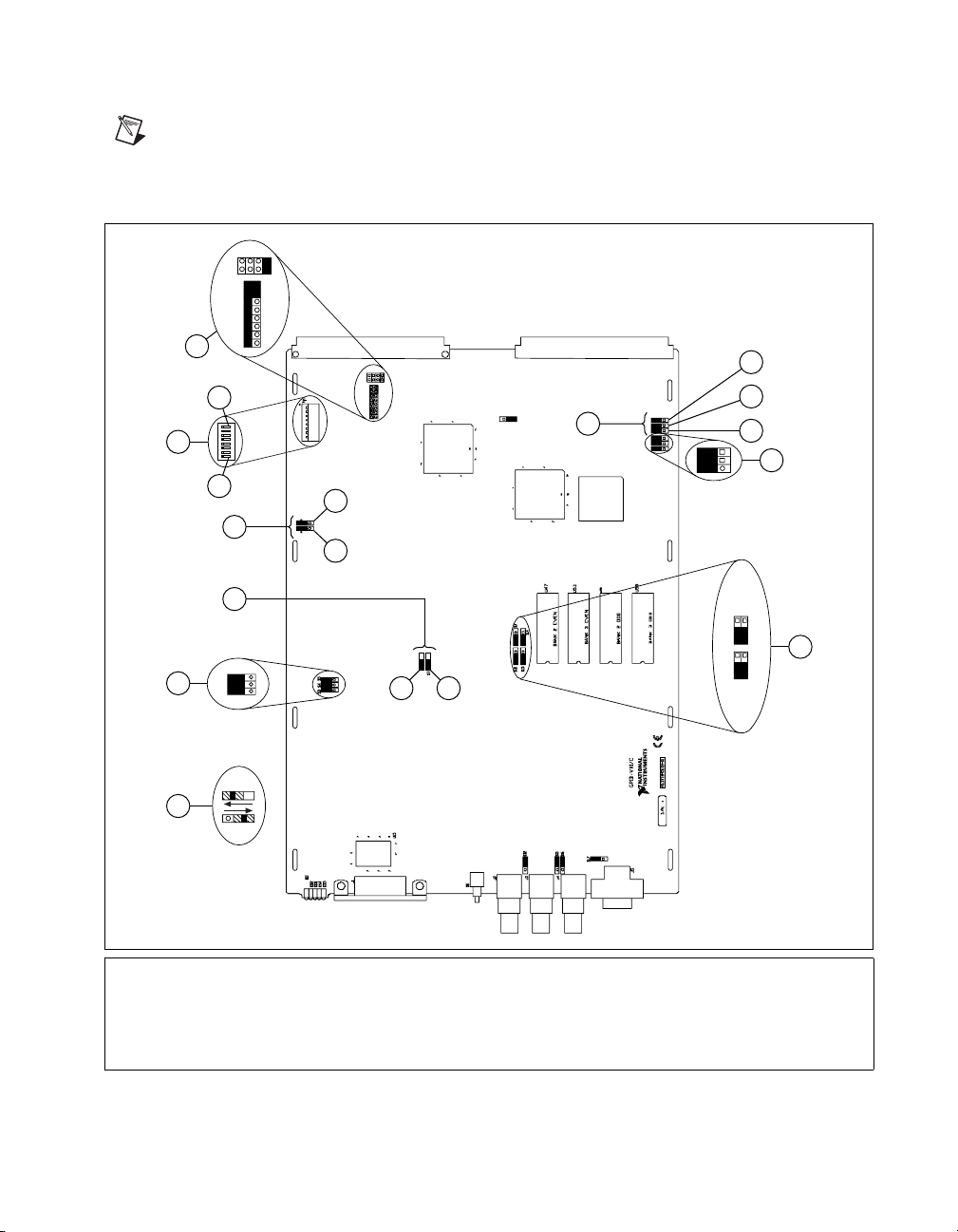
shows the location of the GPIB-VXI/C configurable components and their
physical location relative to some of the major circuit components. The
jumpers and switches are represented in their factory default positions.
GPIB-VXI/C User Manual 2-2 ni.com
Disabled
Enabled
Normally Open
Unterminated
Unterminated
Page 21
Chapter 2 Configuration and Startup Procedures
Note The GPIB-VXI/C is housed in a metal enclosure that has cutouts for access
to all switches and jumpers associated with Slot 0/Non-Slot 0 settings, start-up mode,
and Shared RAM settings. Under normal circumstances, you do not need to open
the enclosure.
W2
W1
1
W2
2
W1
3
4
5
6
S1 S2
7
U31
MIGA
P1
P2
14
15
S9
88070
13
S19 S20 S21 S22 S23 S24
U54
66881
U46
16
17
S20
S19 S21
8
11
S3
S5
S4
12
ON OFF
TNT
1 VXIbus Requester Level
2MSB
3 Logical Address DIP Switch (set to FFh)
4 LSB5 Shared RAM Switches
5S1, S2
6 S2 (OFF)
9 10
COPYRIGHT 1998
7S1 (OFF)
8 Installed RAM Switches
9S6
10 S711Address Modifiers (ON)
11 S3, S4, S5
12 Detail of Switch Settings
13 Slot 0 Switches
14 S24 (ON)
15 S23 (ON)
16 S22 (ON)
17 Startup Mode Switches (ON)
18 EPROM Expansion Switches
Figure 2-1. GPIB-VXI/C Parts Locator Diagram
S11 (ON)
S14 (ON)
BANK 2BANK 3
S13 (ON)
S10 (ON)
18
© National Instruments Corporation 2-3 GPIB-VXI/C User Manual
Page 22

Chapter 2 Configuration and Startup Procedures
Setting the Logical Address, GPIB Primary Address, and Servant Area Size
You can change the logical address, GPIB primary address, and Servant
area size by running the nonvolatile memory configuration utility as
described in the Change Configuration Information section of Chapter 4,
Nonvolatile Configuration.
You can also change the logical address by setting DIP switch SW1.
By default, all the switches are set to the Up position (0xFF). At this setting,
the GPIB-VXI/C reads the logical address from the onboard EEPROM.
To change the logical address, set the switches to the hex value of the
logical address. Switch position 1 is the MSB; 8 is the LSB. Up is logical
1; down is logical 0.
Verifying the Installed RAM Size
The GPIB-VXI/C contains 4 MB of factory-installed local RAM but is
configured to use the minimum amount of 512 KB. Table 2-2 lists the
RAM configurations and their associated switch settings. You can use this
information to change the board configuration.
Table 2-2. Installed RAM Configuration
Installed Memory Size Switch S6 Setting Switch S7 Setting
512 KB OFF OFF
1 MB OFF ON
2 MB ON OFF
4 MB ON ON
GPIB-VXI/C User Manual 2-4 ni.com
Page 23

Chapter 2 Configuration and Startup Procedures
Table 2-3 shows the relationship between the amount of installed memory,
the local address range occupied by the memory, and the range of VXI A24
addresses accessible by the GPIB-VXI/C as a bus master.
Table 2-3. GPIB-VXI/C CPU Local and A24 Memory Ranges
Installed
Memory Size
Installed Memory
Local Address Range
Start End Start End
Accessible VXI A24
Address Range
512 KB 000000h 07FFFFh 080000h E7FFFFh
1 MB 000000h 0FFFFFh 100000h E7FFFFh
2 MB 000000h 1FFFFFh 200000h E7FFFFh
4 MB 000000h 3FFFFFh 400000h E7FFFFh
Setting the Shared Memory Size
You can set the amount of memory that is shared with the VXIbus by
altering the settings of switches S1 and S2. Table 2-4 gives the S1 and S2
switch settings for sharing various portions of RAM with the VXIbus for
each possible installed memory configuration.
Table 2-4. Shared Memory Switch Settings
Amount of Installed Memory Shared with VXIbus
Configured
Memory Size
512 KB 512 KB 256 KB 128 KB none
S1 ON
S2 ON
S1 OFF
S2 ON
S1 ON
S2 OFF
S1 OF
S2 OFF
1 MB 1 MB 512 KB 256 KB none
2 MB 2 MB 1 KB 512 KB none
4 MB 4 MB 2 MB 1 MB none
Note The RAM shared with the VXIbus will be the upper portion of the installed memory.
The GPIB-VXI/C Offset Register holds the shared memory VXI A24 base
address, as described in the VXIbus specification. The RM automatically
configures the Offset Register at startup.
© National Instruments Corporation 2-5 GPIB-VXI/C User Manual
Page 24

Chapter 2 Configuration and Startup Procedures
Setting the Reset Operation
The GPIB-VXI/C has three configurable reset parameters. They can be
enabled or disabled and are as follows:
• Pushbutton resets backplane (asserts SYSRESET* signal).
• Pushbutton resets GPIB-VXI/C (asserts local reset signal).
• Backplane SYSRESET* signal resets GPIB-VXI/C (SYSRESET*
on backplane asserts local reset).
The reset parameters can be altered by the nonvolatile memory
configuration described in the Change Configuration Information
section of Chapter 4, Nonvolatile Configuration.
Setting the VXIbus Requester Level
You can change the VXIbus requester level of the GPIB-VXI/C by moving
the jumpers on jumper blocks W1 and W2 as shown in Figure 2-2.
The GPIB-VXI/C is configured at the factory to be a Level 3 requester.
GPIB-VXI/C User Manual 2-6 ni.com
Page 25
W1
W1
Chapter 2 Configuration and Startup Procedures
W2
a. Level 3 Requester
(Factory Configuration)
W2
W1
W1
Figure 2-2. VXIbus Requester Jumper Settings
Setting the VXI Interrupt Handler Levels
As part of the hardware capabilities on the GPIB-VXI/C, there are three
VXI programmable interrupt handlers. They can be assigned dynamically
by the RM or statically according to the contents of the nonvolatile memory
as described in Chapter 4, Nonvolatile Configuration.
b. Level 2 Requester
W2
c. Level 1 Requester
W2
d. Level 0 Requester
© National Instruments Corporation 2-7 GPIB-VXI/C User Manual
Page 26

Chapter 2 Configuration and Startup Procedures
External Input Termination
Switches S12 and S16 enable a 50-ohm termination to ground for the
external trigger and external clock inputs, respectively. The GPIB-VXI/C
is factory-configured with the termination disabled for both the external
trigger and the external clock inputs. Figure 2-3 shows the settings required
to enable or disable the termination on the external trigger. Figure 2-4
shows the settings required to enable or disable the termination on the
external clock.
S12
a. External Trigger Input Unterminated
(Factory Configuration)
Figure 2-3. External Trigger Input Termination
S16
a. External Clock Input Unterminated
(Factory Configuration)
Figure 2-4. External Clock Input Termination
S12
b. External Trigger Input Terminated
S16
b. External Clock Input Terminated
GPIB-VXI/C User Manual 2-8 ni.com
Page 27

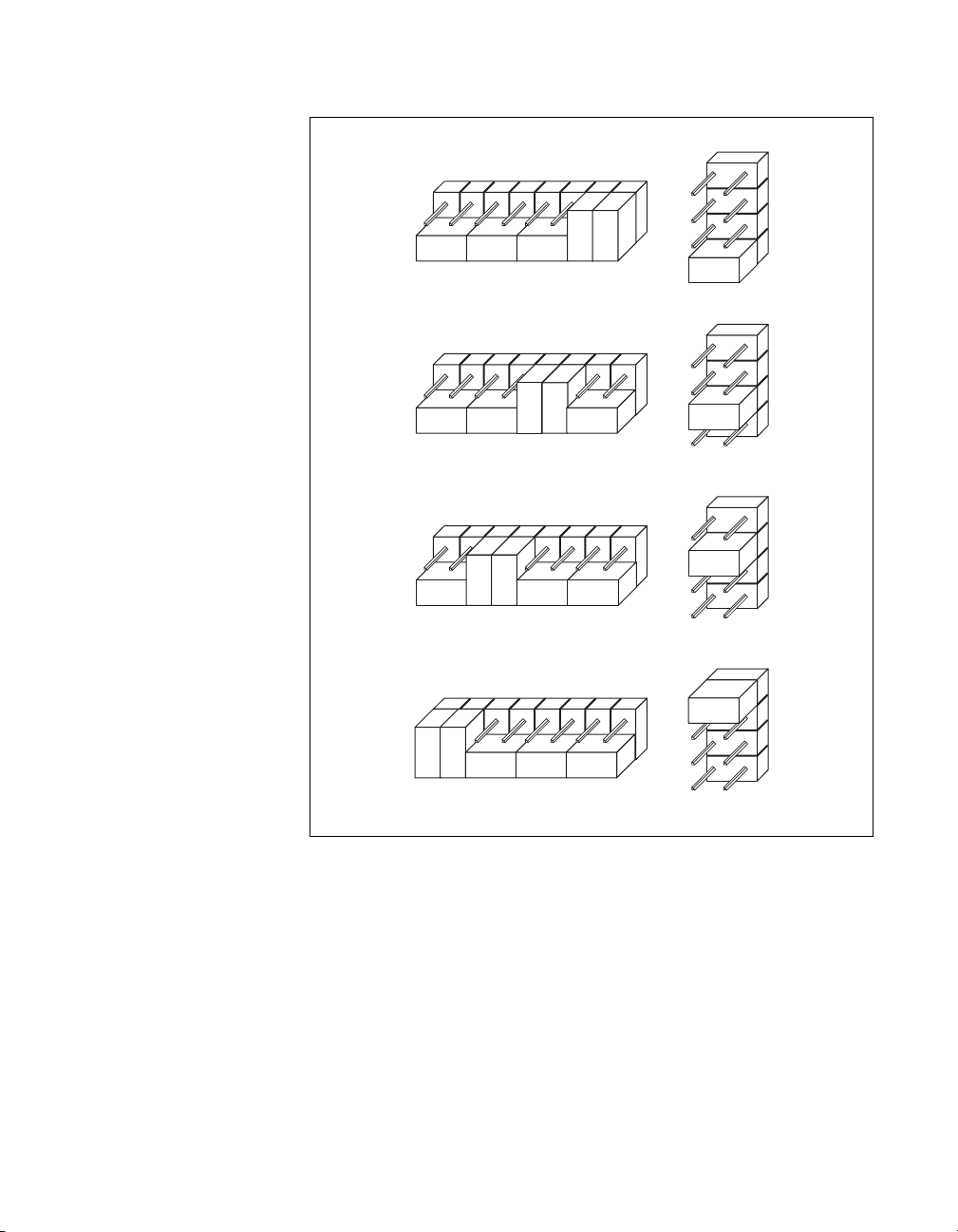
EPROM Configuration
The amount of read-only memory (ROM) in the GPIB-VXI/C can vary
from 512 KB to 1 MB. The standard configuration consists of 512 KB of
EPROM, which is used for the operating firmware. The GPIB-VXI/C also
includes four sockets for EPROM expansion.
The EPROM expansion sockets accommodate combinations of 2764,
27128, 27256, 27512, and 27010 EPROMs. Table 2-5 lists the possible
EPROM memory configurations. Bank 2 has a base address of E80000h
and Bank 3 starts at EC0000h. The maximum EPROM expansion memory
size is 512 KB.
Chapter 2 Configuration and Startup Procedures
Table 2-5. Expansion EPROM Configurations
EPROM
Size
BANK 2
(U47, U55)
BANK 3
(U53, U59)
S11 S14 S10 S13
End
Address
16 KB 2764 None OFF OFF OFF OFF E83FFFh
32 KB 27128 None OFF OFF OFF OFF E87FFFh
64 KB 27256 None OFF ON OFF OFF E8FFFFh
128 KB 27512 None ON ON OFF OFF E9FFFFh
256 KB 27010 None ON ON OFF OFF EBFFFFh
272 KB 27010 2764 ON ON OFF OFF EC3FFFh
288 KB 27010 27128 ON ON OFF OFF EC7FFFh
320 KB 27010 27256 ON ON OFF ON ECFFFFh
384 KB 27010 27512 ON ON ON ON EDFFFFh
512 KB 27010 27010 ON ON ON ON EFFFFFh
When you insert EPROMs into the expansion EPROM slots, orient them
according to the silkscreen printed on the board as shown in Figure 2-1.
The 2764, 27128, 27256 and 27512 EPROMs have fewer pins than the
expansion
sockets. In these cases, align the bottom pins of the EPROM
with the bottom pins of the socket, leaving the top pins open, as illustrated
in Figure 2-5.
Caution Improper EPROM installation can result in damage to the EPROM,
the GPIB-VXI/C, or both.
© National Instruments Corporation 2-9 GPIB-VXI/C User Manual
Page 28
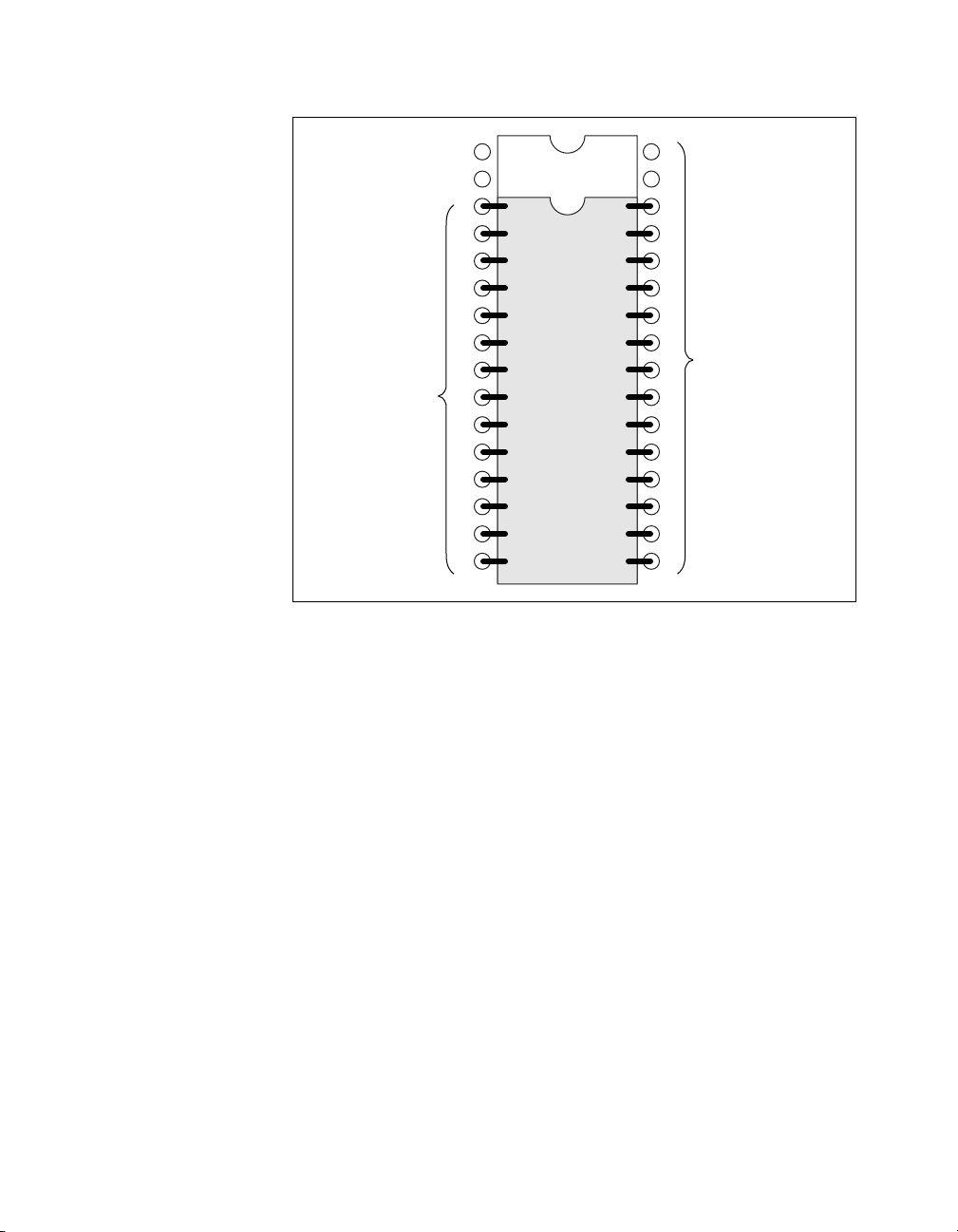
Chapter 2 Configuration and Startup Procedures
EPROM
Figure 2-5. EPROM Insertion Position
Discrete Fault Indicator Configuration
The GPIB-VXI/C comes with a MATE-compatible Discrete Fault
Indicator (DFI). The GPIB-VXI/C monitors the status of the VXIbus
SYSFAIL* signal and relays the status to pins 1 and 6 of the RS-232 serial
port. Refer to Appendix D, Connectors, for more information.
As shown in Figure 2-6 and Table 2-6, switch S17 determines the
relationship between the SYSFAIL* signal and the serial port pins. If S17
is in the OFF position, the GPIB-VXI/C DFI is set to the normally open
mode. Therefore, if SYSFAIL* is not asserted while the backplane is
powered up, pins 1 and 6 will present an electrical open-circuit. In contrast,
if the backplane is unpowered or SYSFAIL* is asserted, pins 1 and 6 will
present an electrical short-circuit.
2764,
27128,
27256,
or
27512
Expansion
EPROM
Socket
If S17 is in the ON position, the GPIB-VXI/C DFI is set to the normally
closed mode. Therefore, if SYSFAIL* is not asserted while the backplane
is powered-up, pins 1 and 6 will present an electrical short-circuit.
In contrast, if the backplane is unpowered or SYSFAIL* is asserted,
pins 1 and 6 will present an electrical open-circuit.
GPIB-VXI/C User Manual 2-10 ni.com
Page 29

Chapter 2 Configuration and Startup Procedures
S17
a. DFI in Normally Open Mode
(Factory Configuration)
Figure 2-6. Discrete Fault Indicator Configuration
Switch S17 Power SYSFAIL Pins 1 and 6
OFF
Figure 2-6a
ON
Figure 2-6b
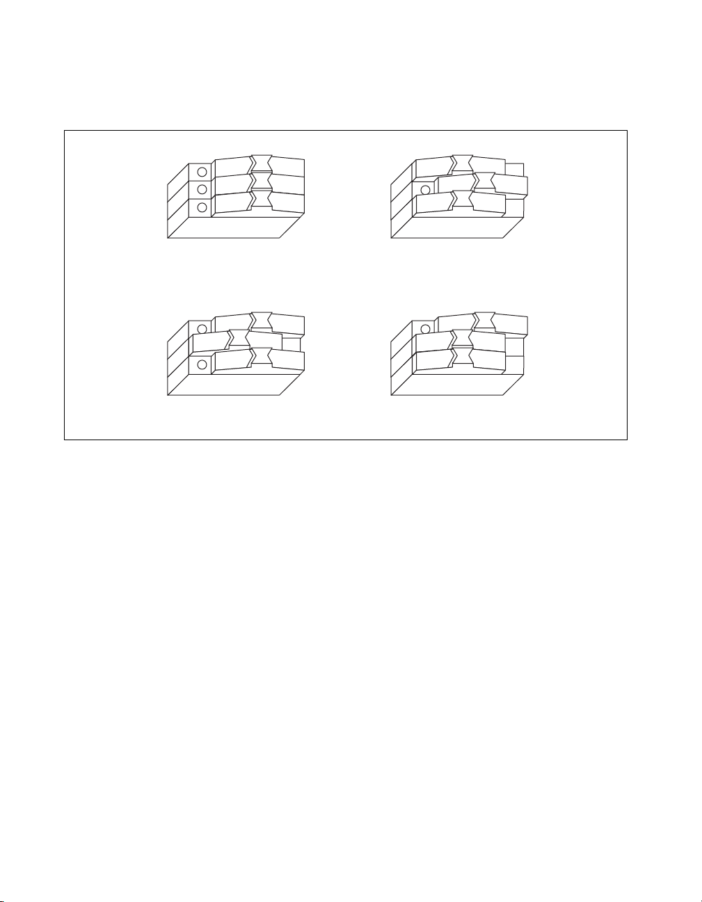
Address Modifier Configuration
By setting onboard switches, you can have the GPIB-VXI/C specify the
state of the VXIbus Address Modifiers during a VXI master access. During
A16 accesses, the lines AM5, AM4, and AM3 are needed high, low, and
high, respectively, and AM1 is needed low. During A24 accesses, the lines
AM5, AM4, and AM3 are all needed high. The GPIB-VXI/C drives the
upper three address modifier lines appropriately for every access. You
should configure the GPIB-VXI/C to drive the lower three address modifier
lines as needed.
S17
b. DFI in Normally Closed Mode
Table 2-6. Discrete Fault Indicator Options
OFF
ON
ON
OFF
ON
ON
N/A
Asserted
Unasserted
N/A
Asserted
Unasserted
Short-Circuit
Short-Circuit
Open-Circuit
Open-Circuit
Open-Circuit
Short-Circuit
© National Instruments Corporation 2-11 GPIB-VXI/C User Manual
Page 30
Chapter 2 Configuration and Startup Procedures
Switches S3, S4, and S5 control the AM0, AM1, and AM2 signals.
Figure 2-7 shows the valid settings of S3, S4, and S5.
S3
S4
S5
a. Supervisor A16, Supervisor A24 Data
(Factory Default Setting)
S3
S4
S5
c. User A16, User A24 Data d. User A16, User A24 Program
Figure 2-7. Address Modifier Signals Switch Settings
GPIB-VXI/C Startup Mode Configuration
Startup mode switches S19 and S20 control the GPIB-VXI/C operation
mode at system startup. They select one of three modes, as shown in
Figure 2-8. The three possible modes of startup are 488-VXI runtime
system mode, nonvolatile configuration mode, and diagnostics mode.
• 488-VXI runtime system mode is the startup mode for normal operation
in a VXI system. The GPIB-VXI/C is configured at the factory to start
up in this mode. The remainder of this chapter contains a description
of operation in this mode.
•In nonvolatile configuration mode, you can edit the contents of the
nonvolatile configuration parameter memory. Refer to Chapter 4,
Nonvolatile Configuration, for more information on the nonvolatile
configuration mode of the GPIB-VXI/C.
•In diagnostics mode, you
on the GPIB-VXI/C. Refer to Chapter 5, Diagnostic Tests, for a
description of the GPIB-VXI/C self-tests.
S3
S4
S5
b. Supervisor A16,
Supervisor A24 Program
S3
S4
S5
can perform extensive offline diagnostic tests
GPIB-VXI/C User Manual 2-12 ni.com
Page 31

Chapter 2 Configuration and Startup Procedures
S20
S19
a. 488-VXI Runtime System Mode
(Factory Configuration)
S20
c. Diagnosis Mode
Figure 2-8. Startup Mode Switch Settings
488-VXI Runtime System Operation
The GPIB-VXI/C is factory configured as a Slot 0 Resource Manager.
The Slot 0 and Resource Manager (RM) functions can be independently
defeated, resulting in four modes of operation:
• Slot 0 Resource Manager (factory configuration)
• Non-Slot 0 Resource Manager
• Non-Slot 0 Message-Based device (non-Resource Manager)
• Slot 0 Message-Based device (non-Resource Manager)
S20
S19
b. Nonvolatile Configuration Mode
S19
This section describes the GPIB-VXI/C configuration procedures and
startup behavior for each mode of operation.
Caution Never install a GPIB-VXI/C configured for Non-Slot 0 operation in Slot 0
or a GPIB-VXI/C configured for Slot 0 operation in any slot other than Slot 0. Doing
so can damage the GPIB-VXI/C, the mainframe, or other modules.
© National Instruments Corporation 2-13 GPIB-VXI/C User Manual
Page 32

Chapter 2 Configuration and Startup Procedures
System Startup Message Printing
The serial port startup printout enable switch S21 controls whether or not
VXI system startup messages are printed to the serial port, as shown in
Figure 2-9. The factory default configuration disables this function.
S21
a. Printing Disabled
(Factory Configuration)
Figure 2-9. VXI System Startup Message Switch Settings
b. Printing Enabled
Slot 0 Resource Manager Configuration
You can configure the GPIB-VXI/C for Slot 0 Resource Manager operation
by enabling the VXIbus Slot 0 functions and setting the logical address
to 0, as shown in Table 2-7.
Table 2-7. Slot 0 Resource Manager Operation Switch and Jumper Settings
Jumper/Switch Position Function
Switches S9 and S15 Refer to Table 2-8. CLK10 routing options.
Switch S22 ON VXI BTO enabled.
Switch S23 ON Bus arbiter and SYSCLK enabled.
CLK10 sourcing for backplane is
enabled.
S21
Switch S24 ON MODID pulled up.
Logical Address Refer to Chapter 4,
Nonvolatile Configuration.
Slot 0 Model Code Refer to Chapter 4,
Nonvolatile Configuration.
GPIB-VXI/C User Manual 2-14 ni.com
Logical address is 0. Set in nonvolatile
configuration or use the DIP switch.
Model code is set to the Slot 0 value.
Set in nonvolatile configuration.
Page 33

Chapter 2 Configuration and Startup Procedures
Table 2-8. CLK10 Routing Options
Switch S15 Switch S59 Function
OFF OFF CLK10 sourced from onboard
clock.
ON OFF CLK10 and EXT CLK connector
sourced from onboard clock.
OFF ON CLK10 sourced from an external
clock via the EXT CLK connector.
ON ON Invalid. Do not use this setting.
Slot 0 Resource Manager Operation
At startup, a GPIB-VXI/C configured as a Slot 0 Resource Manager
performs its self-tests, executes the RM functions, and then enters its
normal mode of operation.
Front Panel LED Indications for RM Operation
The five front panel LEDs are SYSFAIL, FAILED, TEST, ON LINE, and
ACCESS. The GPIB-VXI/C uses the FAILED, TEST, and ON LINE LEDs
to indicate the progress of its self-initialization, self-test, and RM functions.
The LED indications are shown in Table 2-9. A successful system startup
will sequence through the first five states. The point of failure is indicated
for states in which the FAILED LED is lit for an extended period of time.
The LED indications are identical for Slot 0 Resource Manager and
Non-Slot 0 Resource Manager operation.
Table 2-9. Front Panel LED Indications for RM Operation
Sequence FAILED TEST ON LINE State Point of Failure
1 OFF OFF OFF No power Failed before self-test
2 ON OFF OFF In self-initialization Failed in self-test
3 ON ON OFF In self-test —
© National Instruments Corporation 2-15 GPIB-VXI/C User Manual
Page 34

Chapter 2 Configuration and Startup Procedures
Table 2-9. Front Panel LED Indications for RM Operation (Continued)
Sequence FAILED TEST ON LINE State Point of Failure
4 OFF ON ON Performing RM —
5 OFF
ON
ON
OFF
OFF
ON
OFF
ON
ON
ON
ON
OFF
Online
Failed
Failed
In nonvolatile
—
Failed while in RM
Failed while online
—
configuration or
diagnostics mode
The SYSFAIL LED is lit whenever any device in the system is asserting the
VXIbus SYSFAIL* signal.
The ACCESS LED flashes whenever the GPIB-VXI/C is accessed from the
GPIB or from the VXIbus. It also indicates when its MODID is asserted.
Self-Test Operation
The self-test sequence tests the basic functionality of many GPIB-VXI/C
components, including EPROM, RAM, I
channels, GPIB port, interrupt logic, timer, and VXIbus registers (MIGA).
You can execute full tests of the GPIB-VXI/C in diagnostics mode, as
described in Chapter 5, Diagnostic Tests.
2
C bus, RS-232 port, DMA
RM Operation
The RM waits until all devices have stopped driving the VXIbus
SYSFAIL* signal, or until five seconds have elapsed after the VXIbus
SYSRESET* signal is negated. During this period, all of the VXIbus
devices in the system should have completed their self-tests.
Note You can configure the GPIB-VXI/C to wait for any number of seconds before
RM operations begin.
The RM then scans Logical Addresses 1 through 254 for static
configuration devices (SC devices). For each SC device found, it reads
the device class and manufacturer’s ID code from the ID Register and the
model code from the Device Type Register. If the device is an extended
device, the RM reads its Subclass Register. The RM then performs slot
associations for each static configuration device by reading its Status
Register while asserting each MODID line.
GPIB-VXI/C User Manual 2-16 ni.com
Page 35

Chapter 2 Configuration and Startup Procedures
The RM then looks for dynamic configuration devices (DC devices) at
Logical Address 255 by asserting each MODID line and reading the
device’s ID Register. DC devices initially have a logical address of 255.
The RM
subsequently assigns each DC device a different logical address.
For each DC device found, it not only reads the device’s configuration
registers as with SC devices, but also assigns each device the next unused
logical address by writing the appropriate value to the device’s Logical
Address Register. Using the nonvolatile configuration mode, you can set
the starting logical address for the RM to begin assigning DC devices.
Refer to Chapter 4, Nonvolatile Configuration, for more information on
nonvolatile configuration.
If any device has not passed its self-test, the RM forces that device offline
by setting the Sysfail Inhibit and Reset bits in that device’s Control
Register.
The RM then determines the address space of each device by reading its
ID Register. If the device’s address space is A16/A24 or A16/A32, the RM
allocates a section of A24 or A32 memory space to the device according to
the memory requirements indicated by the contents of its Device Type
Register and writes an appropriate value to the device’s Offset Register.
The RM configures the initial Commander/Servant hierarchy according to
each Commander’s Servant area size, using the algorithm described in the
VXIbus specification. The RM issues the appropriate Read Servant Area
and Device Grant commands to each SC Commander. The RM retains all
devices not assigned to other Commanders as its immediate Servants.
Regardless of where DC device logical addresses are assigned, they are
never granted to an SC Commander. The DC Commander/Servant
hierarchy can be created in one of two ways:
• All DC devices can be automatically assigned as Servants of Logical
Address 0 (the Resource Manager).
• A custom hierarchy can be created through the use of the local
command set functions, as described in the Dynamic Configuration
Commands and Queries section of Chapter 3, Local Command Set.
The RM then sends the Read Protocols query to all Message-Based
devices. The response to the query is saved internally for later use in
interrupt handler and GPIB configuration.
The RM configures the VXI interrupter and interrupt handlers using a
seven-entry table contained in nonvolatile configurations. During the
VXI interrupt configuration, the RM assigns interrupt levels to all
Programmable Handlers (PH) and Programmable Interrupters (PI).
© National Instruments Corporation 2-17 GPIB-VXI/C User Manual
Page 36

Chapter 2 Configuration and Startup Procedures
Each entry in the table represents the logical address of the handler that
handles the corresponding level—1 through 7. If the handler is static,
PI Servants are assigned to the level. If the device is a PH device, the RM
assigns both it and any PI Servants to the corresponding level. Notice that
if the table entry is FFh, the level is free to be assigned to any PH device.
If only PH and PI devices are in a system, all entries may contain FFh.
Refer to Chapter 4, Nonvolatile Configuration, for more information.
The remainder of the RM procedure depends upon whether the RM found
any DC devices in the system.
Static Configuration Operation
When all of the previous operations are complete and successful, the RM
sends the Word Serial command Identify Commander to all immediate
Message-Based Servants with bus master capability. At this point, the RM
is ready to bring the system into the Normal Operation sub-state. This is
accomplished by sending the Word Serial query Begin Normal Operation
to all top-level Commanders and immediate Message-Based Servants.
Dynamic Configuration Operation
If the system is a DC system (meaning that at least one DC device was
found), and the nonvolatile configuration specifies that the RM should
create a hierarchy with DC devices assigned to Logical Address 0, the RM
follows the same steps as previously described in the Static Configuration
Operation section. DC devices are treated as SC devices from this point on.
However, if you want to customize your own DC hierarchy and the
nonvolatile configuration specifies that the RM not finish configuring the
hierarchy, the GPIB-VXI/C RM does not send Identify Commander or
Begin Normal Operation to any devices, either static or dynamic.
The outside controller can then create the DC Commander/Servant
hierarchy without having to dynamically reconfigure the system. Use the
GPIB-VXI/C local command
When the system is configured and ready to make a transition to the Normal
Operation sub-state, send the GPIB-VXI/C local command
DCBNOSend sends the Identify Commander and Begin Normal Operation
commands to Message-Based devices as previously described in the Static
Configuration Operation section. Refer to the Dynamic Configuration
Commands and Queries section of Chapter 3, Local Command Set,
for more information about dynamic configuration operation.
The GPIB-VXI/C then performs general configuration operations. The
GPIB-VXI/C creates GPIB address links for its immediate Message-Based
GPIB-VXI/C User Manual 2-18 ni.com
DCGrantDev to create the DC hierarchy.
DCBNOSend.
Page 37

Logical Address
Chapter 2 Configuration and Startup Procedures
SC Servants. After this, the GPIB-VXI/C RM and general configuration
operations are complete.
GPIB Address Assignment
The GPIB-VXI/C automatically assigns GPIB addresses—primary or
secondary—to itself and to each of its immediate Message-Based SC
Servants. If the Message-Based device does not support minimal Word
Serial[I] or VXIbus 488.2[I4] capabilities, no GPIB address link is created.
The GPIB-VXI/C assigns a GPIB address to each device according to the
top five bits of its logical address. For example, the GPIB address of a
device with Logical Address 96 (01100000b) would be 12 (01100b).
If two or more devices have logical addresses with the same top five bits,
the GPIB-VXI/C assigns GPIB addresses to devices in order of the least
significant three bits. Conflicting devices are given the next available GPIB
address. For example, if the GPIB-VXI/C and its Message-Based Servants
have Logical Addresses 0, 24, 27, and 33, the GPIB-VXI/C assigns GPIB
addresses as shown in Table 2-10.
Table 2-10. Example GPIB Address Assignment
3 LSB (Order
of Assignment)
5 MSB GPIB Address
Decimal Binary Binary Binary Decimal
0 00000000b 000b 00000b 0
24 00011000b 000b 00011b 3
33 00100001b 001b 00100b 4
27 00011011b 011b 00011b 5
In the example shown in Table 2-10, the device at Logical Address 27
was assigned GPIB Address 5 because addresses 3 and 4 were previously
assigned. By spacing the GPIB-VXI/C Message-Based Servants at
intervals of eight logical address locations you can avoid situations in
which removing or adding one device changes the GPIB address of another
device.
The default configuration for the GPIB-VXI/C is to use multiple GPIB
secondary addresses (not multiple primary addresses). You can change
the configuration to use multiple primary addresses through nonvolatile
memory configuration as described in the Change Configuration
Information section of Chapter 4, Nonvolatile Configuration.
© National Instruments Corporation 2-19 GPIB-VXI/C User Manual
Page 38

Chapter 2 Configuration and Startup Procedures
You can change the self-assigned default GPIB address of the GPIB-VXI/C
through the nonvolatile memory configuration as described in the Change
Configuration Information section of Chapter 4, Nonvolatile
Configuration. The default GPIB address of the GPIB-VXI/C when
configured for multiple secondary addresses is Secondary Address 0
(Primary Address 1). The default GPIB address of the GPIB-VXI/C,
when configured for multiple primary addresses, is Primary Address 1
(no secondary address).
At times, especially when using multiple primary addressing, you may
find it necessary to avoid particular GPIB addresses to avoid conflicts with
GPIB instruments outside of the VXI mainframe. You can specify what
GPIB addresses to avoid through the nonvolatile memory configuration as
described in the Change Configuration Information section of Chapter 4,
Nonvolatile Configuration.
System Configuration Table
During the execution of the RM and general configuration operations,
the GPIB-VXI/C builds up a table of system configuration information.
Each device has an entry in the table containing the device’s logical
address, its Commander’s logical address, its GPIB address, slot number,
device class, manufacturer ID number, model code, memory space
requirement, memory base address, and memory size. The GPIB-VXI/C
retains this table after the RM and general configuration operations
are complete. The information in the table is accessible through the
GPIB-VXI/C local command set. The GPIB address entry is meaningful
only for immediate Message-Based Servants of the GPIB-VXI/C.
Non-Slot 0 Resource Manager Configuration
Follow these steps to configure the GPIB-VXI/C for Non-Slot 0 Resource
Manager operation. Refer to Table 2-11 for the switch and jumper settings.
1. Disable the VXIbus Slot 0 hardware functions.
2. Set the model code of the GPIB-VXI/C to be configured for
Non-Slot 0 operation using the nonvolatile configuration mode.
3. Set the logical address to 0 in nonvolatile configuration mode or by
using DIP switch SW1.
GPIB-VXI/C User Manual 2-20 ni.com
Page 39

Chapter 2 Configuration and Startup Procedures
Table 2-11. Non-Slot 0 Resource Manager Operation Switch and Jumper Settings
Jumper/Switch Position Function
Switch S15 OFF If S5 is ON, the GPIB-VXI/C also routes
CLK10 to the EXT CLK connector on the
front panel.
Switch S22 OFF VXI BTO disabled.
Switch S23 OFF Bus arbiter and SYSCLK disabled. CLK10
receiving from backplane.
Switch S24 OFF MODID pulled down.
Logical Address Refer to Chapter 4,
Nonvolatile Configuration.
Non-Slot 0
Model Code
Refer to Chapter 4,
Nonvolatile Configuration.
Logical address is 0. Set in nonvolatile
configuration or use the DIP switch.
Model code is set to the Non-Slot 0 value.
Set in nonvolatile configuration.
Non-Slot 0 Resource Manager Operation
The startup sequence for a GPIB-VXI/C configured for Non-Slot 0
Resource Manager operation is nearly identical to the Slot 0 Resource
Manager operation; however, the GPIB-VXI/C controls the Slot 0
resources remotely in Non-Slot 0 RM operation.
A VXIbus Slot 0 device must be in the system. It must be either a
Register-Based device that implements the MODID Register or a
Message-Based device that supports the Word Serial commands Read
MODID, Set Lower MODID, and Set Upper MODID. VXIbus
Specification Revision 1.2 Message-Based Slot 0 devices
are not supported.
Non-Slot 0 Message-Based Device Configuration (Non-Resource Manager)
Follow these steps to configure the GPIB-VXI/C for Non-Slot 0
Message-Based operation. Refer to Table 2-12.
1. Disable the VXIbus Slot 0 functions.
2. Set the model code of the GPIB-VXI/C to be configured for
Non-Slot 0 operation using the nonvolatile configuration mode.
3. Set the logical address to a non-zero value with an appropriate Servant
area size using the nonvolatile configuration mode or by using DIP
switch SW1.
© National Instruments Corporation 2-21 GPIB-VXI/C User Manual
Page 40

Chapter 2 Configuration and Startup Procedures
If the logical address is set to FFh in nonvolatile configuration (the DIP
switch cannot set the logical address to FFh), the GPIB-VXI/C will
participate in dynamic configuration. Otherwise, the GPIB-VXI/C is a
static configuration device.
Table 2-12. Non-Slot 0 Message-Based Device Operation Switch and
Jumper Settings
Jumper/Switch Position Function
Switch S15 OFF If S5 is ON, the GPIB-VXI/C sources
CLK10 at the front panel EXT CLK
connector.
Switch S22 OFF VXI BTO disabled.
Switch S23 OFF Bus arbiter and SYSCLK disabled. CLK10
receiving from backplane.
Switch S24 OFF MODID pulled down.
Logical Address Refer to Chapter 4,
Nonvolatile Configuration.
Non-Slot 0
Model Code
Servant Area
Size
Refer to Chapter 4,
Nonvolatile Configuration.
Refer to Chapter 4,
Nonvolatile Configuration
Non-Slot 0 Message-Based Device Operation
At startup, a GPIB-VXI/C configured as a Non-Slot 0 Message-Based
device performs its self-tests. It then waits until it receives its Device Grant
and Begin Normal Operation Word Serial commands. The RM grants any
logical addresses to the GPIB-VXI/C that reside within its Servant area.
When it responds to the Begin Normal Operation command, the
GPIB-VXI/C enters its normal mode of operation.
Front Panel LED Indications for Message-Based Device Operation
The GPIB-VXI/C indicates the progress of its self-test with the FAILED,
TEST, and ON LINE LEDs. The LED indications are shown in Table 2-13.
A successful system startup sequences through the first five states.
The point of failure is indicated for states in which the FAILED LED is
Logical address is not equal to 0. Set in
nonvolatile configuration or by using
DIP switch SW1.
Model code is set to the Non-Slot 0
value. Set in nonvolatile configuration.
Set appropriate Servant area size.
Set in nonvolatile configuration.
GPIB-VXI/C User Manual 2-22 ni.com
Page 41

Chapter 2 Configuration and Startup Procedures
lit for an extended period of time. The LED indications are identical for
Non-Slot 0 Message-Based device and Slot 0 Message-Based device
operation.
Table 2-13. Front Panel LED Indications for Message-Based Device Operation
Sequence FAILED TEST ON LINE State Point of Failure
1 OFF OFF OFF No power Failed before self-test
2 ON OFF OFF In self-initialization Failed in self-test
3 ON ON OFF In self-test —
4 OFF ON ON Performing RM —
5 OFF
ON
OFF
OFF
OFF
ON
ON
ON
OFF
Online
Failed
In nonvolatile
configuration or
diagnostics mode
Slot 0 Message-Based Device Configuration
Follow these steps to configure the GPIB-VXI/C for Slot 0 Message-Based
operation. Refer to Table 2-14.
1. Enable the VXIbus Slot 0 functions.
2. Set the model code of the GPIB-VXI/C to be configured for Slot 0
operation using the nonvolatile configuration mode.
3. Set the logical address to a non-zero value with an appropriate Servant
area size.
If the logical address is set to FFh in nonvolatile configuration (the DIP
switch cannot set the logical address to FFh), the GPIB-VXI/C will
participate in dynamic configuration. Otherwise, the GPIB-VXI/C is a
static configuration device.
Table 2-14. Slot 0 Message-Based Device Operation Switch and Jumper Settings
Jumper/Switch Position Function
—
Failed while online
—
Switches S9
Refer to Table 2-15. CLK10 routing options.
and S15
Switch S22 ON VXI BTO enabled.
© National Instruments Corporation 2-23 GPIB-VXI/C User Manual
Page 42

Chapter 2 Configuration and Startup Procedures
Table 2-14. Slot 0 Message-Based Device Operation Switch and Jumper Settings (Continued)
Jumper/Switch Position Function
Switch S23 ON Bus arbiter and SYSCLK enabled. CLK10
sourcing backplane.
Switch S24 ON MODID pulled up.
Logical Address Refer to Chapter 4,
Nonvolatile Configuration.
Slot 0 Model
Code
Servant Area
Size
Refer to Chapter 4,
Nonvolatile Configuration.
Refer to Chapter 4,
Nonvolatile Configuration.
Switch S9 Switch S15 Function
OFF OFF CLK10 sourced from onboard clock.
OFF ON CLK10 and EXT CLK connector
ON OFF CLK10 sourced from an external clock
ON ON Invalid. Do not use this setting.
Slot 0 Message-Based Device Operation
At startup, a GPIB-VXI/C configured as a Slot 0 Message-Based device
performs its self-tests. It then waits until it receives its Device Grant
(if any) and Begin Normal Operation Word Serial commands. The RM
grants any logical addresses to the GPIB-VXI/C that reside within its
Servant area. When the GPIB-VXI/C responds to the Begin Normal
Operation command, it enters the normal mode of operation.
Logical address is not equal to 0. Set in
nonvolatile configuration or by using DIP
switch SW1.
Model code is set to the Slot 0 value. Set in
nonvolatile configuration.
Set appropriate Servant area size. Set in
nonvolatile configuration.
Table 2-15. CLK10 Routing Options
sourced from onboard clock.
via the EXT CLK connector.
After the GPIB-VXI/C Passed bit is set, the RM can manipulate or read the
MODID lines by sending the Word Serial queries Read MODID, Set Lower
MODID, or Set Upper MODID to the GPIB-VXI/C.
GPIB-VXI/C User Manual 2-24 ni.com
Page 43

Local Command Set
This chapter contains descriptions of the GPIB-VXI/C local command set. The descriptions
of the commands and queries include syntax, format, and error handling information, as well
as examples of the use of the commands and queries. The local command set supports the
following types of operations:
• System configuration and control
–Help
– General configuration
– Resource Manager (RM) information extraction
– Dynamic system configuration and reconfiguration
– VXI-defined Common ASCII System Commands
– GPIB address configuration
– VXIbus interrupt handler configuration
– IEEE-488.2 common commands
• Instrument development and test
– VXIbus access
– VXI TTL/ECL trigger access
– Word Serial communication
3
Note National Instruments no longer supports Code Instrument (CI) development.
For more information about CI use and development, see the KnowledgeBase link
at
ni.com/documents.
The GPIB-VXI/C command set consists of commands and queries. Commands cause the
GPIB-VXI/C to take some action. A query may also cause the GPIB-VXI/C to take some
action, but it also returns a response containing data or other information.
© National Instruments Corporation 3-1 GPIB-VXI/C User Manual
Page 44

Chapter 3 Local Command Set
Command Set Access
You can execute the local commands from the following ports:
• RS-232
•GPIB
• VXI Word Serial Communication
All ports are active when the GPIB-VXI/C is in the Normal Operation substate and operate
independently of one another. The GPIB-VXI/C returns query responses only to the port
originating the query. The GPIB-VXI/C also maintains a separate status state for each port.
You can use local commands to disable and re-enable each port’s access to the local command
set. The RS-232 port prompts you to enter a local command with the
Command Syntax
The local command set parser is syntactically compatible with the IEEE-488.2 standard.
It will accept numeric parameters in the 488.2 binary, octal, decimal, or hexadecimal formats.
488.2 binary parameters are prefixed with #b. Octal parameters are prefixed with #q, and
hexadecimal parameters are prefixed with #h. Table 3-1 lists the most common numeric
parameter types. The ranges given in Table 3-1 apply unless otherwise specified.
GPIB-VXI> prompt.
Table 3-1. Valid Ranges for Common Numeric Command Parameters
Parameter 488.2 Decimal 488.2 Hexadecimal
<logical address> 0 to 254 #h0 to #hFE
<GPIB address> 0 to 30 #h0 to #h1E
<handler> 1 to 3 #h1 to #h3
<level> 0 to 7 #h0 to #h7
<A16 address> 0 to 65,535 #h0 to #hFFFF
<A24 address> 2,097,152 to 14,680,062 #h200000 to #hE7FFFE
<word value> 0 to 65,535 #h0 to #hFFFF
<byte value> 0 to 255 #h0 to #hFF
<Boolean> 0 or 1 #h0 or #h1
The logical value of a
for the numeric value 1.
GPIB-VXI/C User Manual 3-2 ni.com
<Boolean> parameter is FALSE for the numeric value 0 and TRUE
Page 45

Chapter 3 Local Command Set
The first parameter is delimited from the command name by a space ( ). Additional
parameters are delimited from one another by a comma (
sensitive.
,). The command names are not case
In the command descriptions, parameters are enclosed in angle brackets (
parameters are also enclosed in square brackets (
command.
Multiple commands may be concatenated in a single command line if they are separated with
semicolons (for example,
OBRAM?; DPRAM?<CR>).
Command Line Termination
The serial port command line termination is a carriage return, shown in the subsequent
function descriptions as <CR> (ASCII 0Dh). If the command contains a trailing linefeed,
shown in the subsequent function descriptions as <LF> (ASCII 0Ah), it is ignored. The GPIB
termination is EOI. Commands issued to the GPIB-VXI/C via VXI Word Serial Protocol are
terminated by setting the END bit in the last Byte Available command. Responses are
terminated by setting the END bit in response to the last Byte Request query.
Command and Query Responses
The local commands and queries have two response formats: program mode and console
mode. Program mode responses have a terse data-only format that is intended for a control
program to read and parse. Console responses are returned in the form of readable sentences,
which are better suited for interactive command entry.
You can enable or disable each mode independently, except that one response mode must be
enabled at all times. If both modes are simultaneously enabled, the program response is
returned first, followed by the console response. The local commands used to control the
response modes are
ProgMode and ConsMode.
<>), and optional
[]). Do not enter the brackets as part of the
The response mode configuration is independent for each command source. Table 3-2 lists the
default (startup/reset) response mode configurations.
Table 3-2. Default Response Mode Configurations
Port Response Mode
RS-232 Console mode enabled, program mode disabled
GPIB Program mode enabled, console mode disabled
VXI Word Serial Program mode enabled, console mode disabled
Individual Code Instruments Program mode enabled, console mode disabled
© National Instruments Corporation 3-3 GPIB-VXI/C User Manual
Page 46

Chapter 3 Local Command Set
Command Response Format
Commands do not have program mode responses. They do not return a response to a port
configured for console mode response only, unless the GPIB-VXI/C detects an error
condition.
Console mode command responses are self-explanatory and are not described in this manual.
Query Response Format
Queries have both program and console mode responses. Program mode query responses are
fixed-field formatted, with commas delimiting the fields. For example, the list of logical
addresses returned by the
the field to accommodate the valid range of 0 to 254) separated by commas. The values are
right-justified and padded with the ASCII space character (
Address 45 would be returned as (
decimal.
Console mode query responses are self-explanatory and are not described in this manual.
The query response line termination sequence, shown in the query descriptions as <CRLF>,
indicates an ASCII 0Dh followed by 0Ah.
Laddrs? query is returned as groups of three characters (to allow
45). Unless otherwise noted, all returned values are
) (20h). For example, Logical
Error Reporting
Command syntax and execution errors are reported to the port where the command
originated. If the program response mode is enabled, the GPIB-VXI/C returns an error
message in the following format:
$ <error code><CRLF>
The distinguishing characteristic of a program mode error message is the leading dollar sign
character (
If the console response mode is enabled, the GPIB-VXI/C returns an error message in the
following format:
If both response modes are enabled, the program mode error message is returned first,
followed by the console mode message.
$). A list of error code descriptions is given in Appendix E, Error Codes.
<error description><CRLF>
The Help Query
The Help? query is a quick online reference to the syntax and functionality of the
GPIB-VXI/C local command set.
GPIB-VXI/C User Manual 3-4 ni.com
Page 47

Help?
Purpose
List syntax and descriptions of local command set.
Query Syntax
Help? [<type>[,<type>,....]]
or
Help [<type>[,<type>,....]]
Chapter 3 Local Command Set
<type>
he Help ci Code Instruments
al All sa GPIB address configuration
gc General configuration ih Interrupt handler configuration
dc Dynamic configuration ba VXIbus access
rc Dynamic reconfiguration ws Word Serial communication
rm Resource Manager tr TTL trigger access
cc Common commands
The default type lists the categories available.
Response
The local command set is displayed in the following format:
<Command Syntax> <Command description><CRLF>
<Command Syntax> <Command description><CRLF>
<Command Syntax> <Command description><CRLF>
Example
List syntax and descriptions of general configuration and GPIB address commands.
Help? gc,sa
is the category of command information requested, as follows:
GPIB-VXI Local Command Set<CRLF>
Command/Query Format Description<CRLF>
••
••
••
© National Instruments Corporation 3-5 GPIB-VXI/C User Manual
Page 48

Chapter 3 Local Command Set
General Configuration Commands and Queries
These general configuration commands and queries are described in the following sections:
•
CONF
•
ConsoleEna
•
ConsMode
•
DIAG
•
DPRAM?
•
NVconf?
•
OBRAM?
•
ProgMode
•
WordSerEna
The
ConsMode and ProgMode commands enable and disable the console and program
response modes for the port originating the command.
The
ConsoleEna and WordSerEna commands control access to the local command set from
the RS-232 and VXI Word Serial ports.
The
NVconf? query returns the contents of the onboard nonvolatile memory. CONF reboots
the GPIB-VXI/C and enters the nonvolatile configuration editor.
DIAG reboots the GPIB-VXI/C and enters diagnostic mode.
The
OBRAM? query can be used to determine the amount of GPIB-VXI/C installed RAM,
and the
DPRAM? query returns the amount of the installed RAM that is shared with VXI
A24 space.
GPIB-VXI/C User Manual 3-6 ni.com
Page 49

CONF
Purpose
Reboot into nonvolatile configuration mode.
Command Syntax
CONF
Example
Reboot into nonvolatile configuration mode.
CONF
ConsoleEna
Purpose
Enable or disable the RS-232 port as the console.
Command Syntax
ConsoleEna <Boolean>
Chapter 3 Local Command Set
Action
If <Boolean> is TRUE, ConsoleEna sets the RS-232 port to be a local command set input.
If
<Boolean> is FALSE, ConsoleEna disables the RS-232 port connection to the local
command set. Notice that once the console has been disabled, it must be re-enabled from
a command source other than the RS-232 port (such as the GPIB port).
Examples
Disable console.
ConsoleEna 0
Enable console.
ConsoleEna 1
© National Instruments Corporation 3-7 GPIB-VXI/C User Manual
Page 50

Chapter 3 Local Command Set
ConsMode
Purpose
Enable or disable the console data mode.
Command Syntax
ConsMode <Boolean>
Action
If <Boolean> is TRUE, ConsMode enables console format responses for the command
source issuing the command.
If
<Boolean> is FALSE, ConsMode disables console format responses for the command
source issuing the command.
The console response mode applies only to the response path connected to the
command source. For example, disabling the console response mode from the GPIB port
does not affect the response mode on the serial port.
Example
Disable console format responses.
ConsMode 0
Enable console format responses.
ConsMode 1
DIAG
Purpose
Reboot into diagnostics mode.
Command Syntax
DIAG
Example
Reboot into diagnostics mode.
DIAG
ConsMode
GPIB-VXI/C User Manual 3-8 ni.com
Page 51

DPram?
Purpose
Get the A24/A32 starting address and the size of the GPIB-VXI/C VXI shared RAM.
Query Syntax
DPram?
Response
Program response:
<A24/A32 starting address>, <shared RAM size><CRLF>
Console response:
This GPIB-VXI has <shared RAM size>K bytes dual ported to [A24, A32]
Address <A24/A32 hex starting address>
where
format,
<shared RAM size> is in KB.
Chapter 3 Local Command Set
<CRLF>
<A24/A32 starting address> is the shared RAM base address in decimal integer
<A24/A32 hex starting address> is in C language hexadecimal format.
© National Instruments Corporation 3-9 GPIB-VXI/C User Manual
Page 52

Chapter 3 Local Command Set
NVconf?
Purpose
Display the contents of the nonvolatile (NV) configuration parameter memory.
Query Syntax
NVconf?
Response
The contents of the onboard EEPROM are displayed in the following format:
=============== Nonvolatile Configuration Information ===============
Logical Address: 0x 0 Device Type : Message Based
Manufacturer Id: 0xff6 Model Code : 0x ff (Slot 0)
Slave Addr Spc : A24 Protocol Reg : 0x ff0
RESET Config : PBtoLocalRESET PBtoSYSRESET SYSRESETtoLocalRESET
Serial Number : 0x 10003 User pROBE Pars: 0x 0 (None)
Region 1 Size : 0x070000 Number Procs : 32
Number Exchgs : 32 Number Msgs : 384
Console : Enabled
VXI Interrupt Level To Handler Logical Address (0xff = free to
assign):
1:0xff, 2:0xff, 3:0xff, 4:0xff, 5:0xff, 6:0xff, 7:0xff
A24 Assign Base: 0x200000 A32 Assign Base: 0x20000000
DC Starting LA : 0x 1, BNO=YES For FAILED Dev : DO set Reset Bit
Servant Area : 0x 0 GPIB Primary : 0x 1
GPIB Addr Assgn: Default GPIB Flags : NAT4882 DMA
CI Block Base : 0x 80000 CI Num Blocks : 0
------ Resident Code Instrument Locations ------
# 0: 0 # 1: 0 # 2: 0
# 3: 0 # 4: 0 # 5: 0
# 6: 0 # 7: 0 # 8: 0
# 9: 0 # a: 0 # b: 0
GPIB-VXI/C User Manual 3-10 ni.com
Page 53

Chapter 3 Local Command Set
------ CI Nonvolatile User Configuration Variables ------
# 0: 0 # 1: 0 # 2: 0 # 3: 0
# 4: 0 # 5: 0 # 6: 0 # 7: 0
# 8: 0 # 9: 0 #10: 0 #11: 0
#12: 0 #13: 0 #14: 0 #15: 0
#16: 0 #17: 0 #18: 0 #19: 0
#20: 0 #21: 0 #22: 0 #23: 0
#24: 0 #25: 0 #26: 0 #27: 0
#28: 0 #29: 0 #30: 0 #31: 0
OBram?
Purpose
Get the amount of RAM installed onboard the GPIB-VXI/C.
Query Syntax
OBram?
Response
Program response:
<memsize><CRLF>
<memsize> is the amount of installed RAM, in KB.
where
Console response:
This GPIB-VXI has <expression> of RAM installed onboard.<CRLF>
<expression> is the amount of installed RAM.
where
© National Instruments Corporation 3-11 GPIB-VXI/C User Manual
Page 54

Chapter 3 Local Command Set
ProgMode
Purpose
Enable or disable the program data mode.
Command Syntax
ProgMode <Boolean>
Action
If <Boolean> is TRUE, ProgMode enables program format responses for the command
source issuing the command.
If
<Boolean> is FALSE, ProgMode disables program format responses for the command
source issuing the command.
The program response mode applies only to the response path connected to the
command source. For example, disabling the program response mode from the GPIB port
does not affect the response mode on the serial port.
Examples
Disable program format responses.
ProgMode 0
Enable program format responses.
ProgMode 1
ProgMode
GPIB-VXI/C User Manual 3-12 ni.com
Page 55

WordSerEna
Purpose
Assign control of the GPIB-VXI/C physical Word Serial registers to an onboard logical
address (GPIB-VXI/C command interpreter or code instrument).
Command Syntax
WordSerEna <logical address>
Action
Control of the physical Word Serial registers is passed to <logical address>. <logical
address>
The default control of the physical registers is given to the GPIB-VXI/C local command
set parser.
Examples
Pass control of the physical registers to code instrument at Logical Address 5.
WordSerEna 5
Chapter 3 Local Command Set
must be the logical address of the GPIB-VXI/C or an onboard code instrument.
Pass control of the physical registers back to GPIB-VXI/C local command parser at Logical
Address 0.
WordSerEna 0
© National Instruments Corporation 3-13 GPIB-VXI/C User Manual
Page 56

Chapter 3 Local Command Set
RM Information Queries
These RM information queries are described in the following sections:
•
A24MemMap?
•
A32MemMap?
•
Cmdr?
•
CmdrTable?
•
Laddrs?
•
NumLaddrs?
•
RmEntry?
•
Srvnts?
•
StatusState?
Note The system information commands (NumLaddrs?, Laddrs?, CmdrTable?,
A24MemMap?, and A32MemMap?) return information about the known system. If
the GPIB-VXI/C is the system RM, it can access information about the entire system.
If it is not the RM, it has information only about itself and its immediate Servants.
Numladdrs? query is used to find out how many devices there are in the system.
The
The number of devices could then be used by a control program to determine the allocation
size for an array that is to hold the logical addresses of each device.
The
Laddrs? query returns a list of logical addresses for devices in the system.
The
RmEntry?, Srvnts?, Cmdr?, and StatusState? queries return RM information for a
particular device.
The
CmdrTable? query returns the system hierarchy table.
The
A24MemMap? and A32MemMap? queries return the A24 and A32 memory
configuration lists.
GPIB-VXI/C User Manual 3-14 ni.com
Page 57

A24MemMap?
Purpose
Get the A24 address space allocation for the system.
Query Syntax
A24MemMap?
Response
Program response:
<la1>,<A24 memory base>,<A24 memory size><CRLF>
<la2>,<A24 memory base>,<A24 memory size><CRLF>
•
•
<laN>,<A24 memory base>,<A24 memory size><CRLF>
where
<la1> through <laN> are logical addresses containing A24 address space.
Console response:
A24 Memory Map is as follows:<CRLF>
Logical Address <la1> has <A24 memory size>K
<A24 memory size> bytes) at A24 Address<A24 memory base>
•
•
Logical Address <la
(<A24 memory size> bytes) at A24 Address<A24 memory base>
N
> has <A24 memory size>K
Chapter 3 Local Command Set
<CRLF>
<CRLF>
Example
Get A24 address map for the system.
A24MemMap?
© National Instruments Corporation 3-15 GPIB-VXI/C User Manual
Page 58

Chapter 3 Local Command Set
A32MemMap?
Purpose
Get the A32 address space allocation for the system.
Query Syntax
A32MemMap?
Response
Program response:
<la1>,<A32 memory base>,<A32 memory size><CRLF>
<la2>,<A32 memory base>,<A32 memory size><CRLF>
•
•
<la
N
>,<A32 memory base>,<A32 memory size><CRLF>
where
<la1> through <laN> are logical addresses containing A32 address space.
Console response:
A32 Memory Map is as follows:<CRLF>
Logical Address <la1> has <A32 memory size>K
(<A32 memory size> bytes) at A32 Address<A32 memory base>
•
•
Logical Address <la
(<A32 memory size> bytes) at A32 Address<A32 memory base>
N
> has <A32 memory size>K
<CRLF>
<CRLF>
Example
Get A32 address map for the system.
A32MemMap?
GPIB-VXI/C User Manual 3-16 ni.com
Page 59

Cmdr?
Purpose
Get the logical address of a device’s Commander.
Query Syntax
Cmdr? <logical address>
where <logical address> is the logical address of the device.
Response
Program response:
<Commander's logical address><CRLF>
Console response:
The Commander of Logical Address <logical address> is Logical Address
<Commander's logical address>
Example
Get the Commander’s logical address for Logical Address 15.
Cmdr? 15
Chapter 3 Local Command Set
<CRLF>
© National Instruments Corporation 3-17 GPIB-VXI/C User Manual
Page 60

Chapter 3 Local Command Set
CmdrTable?
Purpose
Get the known system hierarchy table.
Query Syntax
CmdrTable?
Response
Program response:
<cla0>,<cla1>,<cla2>,<cla3>,<cla4>, . . .,<cla254><CRLF>
where <cla
N
> is either the Commander’s logical address for Logical Address N, or 0 for
top-level Commanders and unused logical addresses. Notice that no value is returned for
Logical Address 255.
Console response:
Known Hierarchy is as follows:<CRLF>
Logical address <la1> has Servants: <sa1,1>,...,<sa1,M>
<comment>
Logical address <la2> has Servants: <sa2,1>,...,<sa2,M>
<comment>
<CRLF>
<CRLF>
•
•
Logical address <la
<comment>
where
The
<comment> field indicates any relevant information about the status and/or capabilities
<CRLF>
<la X> is a valid logical address with Servant addresses <sa X,1> through <sa1,M>.
of the device at Logical Address
N
> has Servants: <saN,1>,...,<saN,M>
<laX>.
GPIB-VXI/C User Manual 3-18 ni.com
Page 61

Laddrs?
Purpose
Get a list of the known logical addresses.
Query Syntax
Laddrs?
Response
Program response:
<la1>,<la2>,..., <laN><CRLF>
where
Console response:
Known logical addresses are: <la1>,<la2>,..., <laN><CRLF>
CI logical addresses are terminated with an asterisk (*) in the console mode response.
Chapter 3 Local Command Set
<la1> through <laN> are the known logical addresses.
NumLaddrs?
Purpose
Get the number of known logical addresses.
Query Syntax
NumLaddrs?
Response
Program response:
<num las><CRLF>
<num las> is the number of known logical addresses.
where
Console response:
There are <num las> known Logical Addresses<CRLF>
© National Instruments Corporation 3-19 GPIB-VXI/C User Manual
Page 62

Chapter 3 Local Command Set
RmEntry?
Purpose
Return RM information about a device or all devices. RmEntry? does not return the
Servant list.
Query Syntax
RmEntry? [<logical address>]
If <logical address> is omitted, RmEntry? returns the RM information for all devices.
Response
Program response:
<la>,<cla>,<sa>,<slot>,<devclass>,<subclass>,<manID>,<modelcode>,
<memspace>,<membase>,<memsize>,<state>,<line status>
Console response:
Resource manager entry for Logical Address <logical address>:<CRLF>
<CRLF>
Commander's Logical Address :<cla><CRLF>
GPIB Secondary Address :<addr><CRLF>
Slot :<slot><CRLF>
Device class :<devclass> (class)<CRLF>
Extended Sub Class :<subclass><CRLF>
Manufacturer's ID :<manID> (manufacturer's name)<CRLF>
Model code :<modelcode><CRLF>
A16/A24/A32 Memory space :<memspace> (memory space)<CRLF>
A24/A32 Memory Base :<membase><CRLF>
A24/A32 Memory Size :<memsize>K (<memsize> bytes)<CRLF>
Status State :<state> (state)<CRLF>
Forced Offline? :<line status> (yes/no)<CRLF>
<CRLF>
The mnemonics have the following meanings:
la Device’s logical address
cla Commander’s logical address
addr Device’s GPIB address (255 if not assigned GPIB address)
slot Slot number (255 if unknown, such as if the device does not have
MODID capability)
GPIB-VXI/C User Manual 3-20 ni.com
Page 63

Chapter 3 Local Command Set
devclass Device class; the following values may be used:
0 = Memory Class
1 = Extended Class
2 = Message-Based
3 = Register-Based
subclass Extended class device’s subclass
manID Manufacturer’s ID number
modelcode Device’s manufacturer-assigned model code
memspace Memory space requirement:
0 = A16 only
1 = A16/A24
2 = A16/A32
membase Memory base address
memsize Memory size in bytes
state Status state:
0 = Failed and not Ready
1 = Passed and not Ready
2 = Failed and Ready
3 = Passed and Ready
line status Online/offline status:
0 = online
1 = forced offline
The program mode response format is the same for all devices. However, the console mode
response returns only the lines that are relevant. For example, memory base address and
memory size lines are not returned for A16-only memory space devices.
Example
Get RM information for a device at Logical Address 78.
RmEntry? 78
© National Instruments Corporation 3-21 GPIB-VXI/C User Manual
Page 64

Chapter 3 Local Command Set
Srvnts?
Purpose
Get a list of a device’s Servants.
Query Syntax
Srvnts? <logical address>
<logical address>
Response
Program response:
<sla1>,<sla2>,...,<slaN><CRLF>
where
Console response:
Logical Address <logical address> has servants:
<sla1>, <sla2>,..., <sla
if the device has Servants, or
Logical Address <logical address> has servants:
none <comment>
if the device has no Servants.
The
of the device.
Example
Get a list of Servants for device at Logical Address 15.
Srvnts? 15
is the device’s logical address.
<sla1> through <slaN> are the Servant device logical addresses.
N
> <comment><CRLF>
<CRLF>
<comment> field indicates any relevant information about the status and/or capabilities
GPIB-VXI/C User Manual 3-22 ni.com
Page 65

StatusState?
Purpose
Get a device’s current self-test status.
Query Syntax
StatusState? <logical address>
Chapter 3 Local Command Set
<logical address>
Response
Program response:
<val><CRLF>
The value of
containing the Ready and Passed bits.
0 The device is Failed and not Ready.
1 The device is Passed and not Ready.
2 The device is Failed and Ready.
3 The device is Passed and Ready.
Console response:
Device at Logical Address <logical address> is Failed and not
Ready
or
Device at Logical Address <logical address> is Passed and not
Ready
or
Device at Logical Address <logical address> is Failed and Ready<CRLF>
is the logical address for the device.
<val> is equivalent to the value of the field in the device’s status register
<val> can be interpreted as follows:
<CRLF>
<CRLF>
or
Device at Logical Address <logical address> is Passed and Ready<CRLF>
Example
Get self-test status for device at Logical Address 48.
StatusState? 48
© National Instruments Corporation 3-23 GPIB-VXI/C User Manual
Page 66

Chapter 3 Local Command Set
Dynamic Configuration Commands and Queries
These dynamic configuration (DC) commands and queries are described in the following
sections:
•
DCBNOSend
•
DCGrantDev
•
DCSystem?
The DC commands are used to configure the VXI system when all of these conditions are
present:
• The GPIB-VXI/C is the RM.
• At least one DC device is present in the system.
• The nonvolatile configuration setup specifies not to send Begin Normal Operation
(user-specified hierarchy).
• The system is still in the startup Configure substate (
The
DCSystem? query response indicates whether the system contains a DC device. If the
system is found to be a DC system, the
Commander/Servant hierarchy. The
DCGrantDev command is used to configure the
DCBNOSend command is used to end the DC phase and
to cause the system to enter normal operation.
DCBNOSend has not been sent).
GPIB-VXI/C User Manual 3-24 ni.com
Page 67

DCBNOSend
Purpose
Cause a DC system to exit the Configure substate and enter the Normal Operation substate.
Command Syntax
DCBNOSend
Action
Send the Begin Normal Operation command to all top-level Commanders.
DCGrantDev
Purpose
Grant a device to a Message-Based Commander in a DC system. DCGrantDev can be used
only to configure the initial Commander/Servant hierarchy of a DC system, and before
DCBNOSend is used to cause the system to enter the Normal Operation substate.
Chapter 3 Local Command Set
Command Syntax
DCGrantDev <Commander's logical address>,
<Servant's logical address>
Action
DCGrantDev sends the Device Grant command to the Commander at <Commander's
logical address>
, granting it the device at <Servant's logical address>.
Example
Grant Servant at Logical Address 7 to Commander at Logical Address 5.
DCGrantDev 5,7
© National Instruments Corporation 3-25 GPIB-VXI/C User Manual
Page 68

Chapter 3 Local Command Set
DCSystem?
Purpose
Determine if the system is a DC system. A system is DC if it has at least one DC device.
Query Syntax
DCSystem?
Response
Program response:
1 <CRLF>
if it is a DC system, or
0 <CRLF>
if it is not a DC system, or if it is no longer dynamically configurable because the Begin
Normal Operation command has already been sent to the top-level Commanders through
the
DCBNOSend local command.
Console response:
This IS a Dynamic Configured system.<CRLF>
if it is a DC system, or
This is NOT a Dynamic Configured system.<CRLF>
if it is not a DC system.
GPIB-VXI/C User Manual 3-26 ni.com
Page 69

Dynamic Reconfiguration Queries
These dynamic reconfiguration queries are described in the following sections:
•
Broadcast?
•
GrantDev?
•
RelSrvnt?
The dynamic reconfiguration commands are used to reconfigure the GPIB-VXI/C’s Servant
subtree after the system has entered the Normal Operation substate. If the GPIB-VXI/C is
RM, these commands can be used to reconfigure the entire system.
The
Broadcast? query can be used to make the system or subtree enter the Configure
substate by broadcasting the End Normal Operation Word Serial query, or the Clear Word
Serial command followed by the Abort Normal Operation Word Serial query.
The
RelSrvnt? and GrantDev? queries can then be used to restructure the
Commander/Servant hierarchy. You could perform dynamic reconfiguration directly by using
the
WSCmd and WSCmd? local commands, but the GPIB-VXI/C’s RM table would not be
updated. By using the
you ensure that the GPIB-VXI/C’s system hierarchy and GPIB address link records do not
become corrupted.
RelSrvnt? and GrantDev? queries to reconfigure the system,
Chapter 3 Local Command Set
You can return the system or subtree to the Normal Operation substate by using the
Broadcast? query to broadcast the Identify Commander and Begin Normal Operation
Word Serial commands.
© National Instruments Corporation 3-27 GPIB-VXI/C User Manual
Page 70

Chapter 3 Local Command Set
Broadcast?
Purpose
Broadcast dynamic reconfiguration, initialization, or termination Word Serial commands to
the GPIB-VXI/C’s Message-Based Servants or to all top-level Commanders in the system.
Query Syntax
Broadcast? <Boolean>,<ws cmd>
If <Boolean> is 1, the GPIB-VXI/C broadcasts <ws cmd> to all top-level Commanders.
If
<Boolean> is 0, it broadcasts <ws cmd> to its Message-Based Servants. Notice that the
GPIB-VXI/C should only broadcast to top-level Commanders when it is RM.
The
Broadcast? query can fail due to inability to complete a Word Serial operation,
or because an invalid code was returned from a device in response to ANO or ENO.
<ws cmd> is a mnemonic as follows.
<ws cmd> Word Serial Command Name Ty pe
ANO Abort Normal Operation Query
BNO Begin Normal Operation Query
CLR Clear Command
ENO End Normal Operation Query
IDN Identify Commander Command
Response
Program response:
<CRLF>
if the command was successful, or
<la>,<cmd val>,<ws response>,<ws error code>
if the command failed.
Console response:
Done broadcasting Word Serial command: <Word Serial command name>.
GPIB-VXI/C User Manual 3-28 ni.com
Page 71

Chapter 3 Local Command Set
if the command was successful, or
Logical address <la> returned <ws response> from ENO (Unable to halt)
or
Logical address <la> returned <ws response> from ANO (Invalid
response)
or
Error sending Logical Address <la> Word Serial command <hex cmd
val><CRLF><space><space><ws error>
<CRLF>
if the command failed.
<la> is the logical address of the device to which the broadcast failed.
<cmd val> is the value of the Word Serial command, in decimal. <hex cmd val> is the
value in hexadecimal.
For Word Serial queries,
Address
<Word Serial command name> is the name of the command name as shown in the
<la>. For Word Serial commands <ws response> is 0.
<ws response> is the Word Serial response of the device at Logical
previous table.
<ws error code> is a decimal value that can be interpreted by converting it to a binary bit
pattern. A value of 1 in the bit positions shown in the following table indicates that an error
occurred during the attempt to broadcast the Word Serial command.
Bit Word Serial Error
0 Word Serial command completed successfully (no Word Serial error)
1 Timeout waiting to send Word Serial command to device at <la>
2 Timeout waiting for Word Serial response from device at <la>
3 Device at <la> did not recognize the command
6 Multiple query error
10 Read Protocol error not supported
13 Read Ready (RR) violation
14 Write Ready (WR) violation
© National Instruments Corporation 3-29 GPIB-VXI/C User Manual
Page 72

Chapter 3 Local Command Set
None of the other bits has significance in this context.
<ws error> is a string explaining the Word Serial error as shown in the previous table.
Example
Broadcast the Identify Commander Word Serial command to all top-level Commanders.
broadcast? 1,IDN
GPIB-VXI/C User Manual 3-30 ni.com
Page 73

GrantDev?
Purpose
Grant a Servant to a Commander.
Query Syntax
GrantDev? <Commander's logical address>, <Servant's logical address>
Action
Grants the device at <Servant's logical address> to device at <Commander's
logical address>
Chapter 3 Local Command Set
.
The GPIB-VXI/C must own the device at
The GPIB-VXI/C can get ownership of any device with the
Notice that before the
query, or a Clear command followed by the Abort Normal Operation query should have
been broadcast with the
Response
Program response:
0<CRLF>
indicates that the command was successful.
Console response:
Logical Address <Commander's logical address> granted device at
Logical Address <Servant's logical address>.
Example
Grant Device 16 to Commander at Logical Address 8.
Grantdev? 8,16
<Servant's logical address>.
RelSrvnt? command.
GrantDev? query is used, the Word Serial End Normal Operation
Broadcast? query.
© National Instruments Corporation 3-31 GPIB-VXI/C User Manual
Page 74

Chapter 3 Local Command Set
RelSrvnt?
Purpose
Recover a Servant from a Commander.
Query Syntax
RelSrvnt? <Commander's logical address>, <Servant's logical address>
Action
Commands device at <Commander's logical address> to release ownership of the
device at
device.
Response
Program response:
65534<CRLF>
if the Commander released the Servant. Any other response indicates that an error occurred.
Console response:
Logical Address <Commander's logical address> released device at
Logical Address <Servant's logical address>.
<Servant's logical address>. The GPIB-VXI/C assumes ownership of the
Example
Recover Servant at Logical Address 16 from Commander at Logical Address 8.
Relsrvnt? 8,16
GPIB-VXI/C User Manual 3-32 ni.com
Page 75

Chapter 3 Local Command Set
VXI-Defined Common ASCII System Commands
These VXI-defined Common ASCII System Commands and Queries are described in the
following sections:
•
DCON?
•
DINF?
•
DLAD?
•
DNUM?
•
DRES?
•
RREG?
•
WREG
You can use these commands and queries to retrieve device information/configuration,
perform a soft reset, and peek/poke a device’s registers.
The
DNUM? query is used to find out how many devices are in the system. The DLAD? query
returns a list of logical addresses for devices in the system.
The
DINF? query returns static information about a device. The DCON? query returns
configuration information about a device.
The
DRES? query is used to perform a soft-reset sequence on a device.
The
RREG? query and WREG command are used to peek (read from) and poke (write to)
registers on a VXI device.
© National Instruments Corporation 3-33 GPIB-VXI/C User Manual
Page 76

Chapter 3 Local Command Set
DCON?
Purpose
Return system configuration information about a device or all devices.
Query Syntax
DCON? [<logical address>]
If <logical address> is omitted, DCON? returns the configuration information for all
devices.
Response
Program response:
<la1>,<cla>,<IHANS>,<INTS>,<status>,<sstate>,<com><CRLF>
Console response:
Device configuration at Logical Address <la>: <CRLF>
<CRLF>
Commander's Logical Address :<cla><CRLF>
Interrupt Handlers :<IHANS><CRLF>
Interrupters :<INTS><CRLF>
Passed/Failed/Ready :<status><CRLF>
Device Substate :<sstate><CRLF>
Manufacturer Specific Comment :<com><CRLF>
The mnemonics have the following meanings:
la Device’s logical address
cla Commander’s logical address
IHANS Interrupt handler levels used by this device where IHANS is a
7-digit binary representing the seven VXI interrupt levels and a
1 in each position, meaning Interrupt Handler present
INTS Interrupter levels used by this device where INTS is a 7-digit
binary representing the seven VXI interrupt levels and a 1 in
each position, meaning Interrupter present
status Status state of the device:
PA SS
FAIL
IFAIL
READY
GPIB-VXI/C User Manual 3-34 ni.com
Page 77

Example
Chapter 3 Local Command Set
sstate Substate of the device
NOP
CONF
NONE
com Not used; always returns ""
Get device configuration information for Logical Address 6.
DCON? 6
© National Instruments Corporation 3-35 GPIB-VXI/C User Manual
Page 78

Chapter 3 Local Command Set
DINF?
Purpose
Return static system information about a device.
Query Syntax
DINF? [<logical address>]
If <logical address> is omitted, DINF? returns static information for all devices.
Response
Program response:<CRLF>
<la1>,<manID>,<modelcode>,<devclass>,<memspace>,<membase>,
<memsize>,<slot>,<slot0>,<ext>,<attr>,<com>
Console response:
Device configuration at Logical Address <la>:<CRLF>
<CRLF>
Manufacturer ID Number :<manid> (manufacturer name)<CRLF>
Model Code :<modelcode><CRLF>
Device Class :<devclass><CRLF>
A16/A24/A32 Memory Space :<memspace><CRLF>
A16/A24/A32 Memory Base :<membase><CRLF>
A16/A24/A32 Memory Size :<memsize><CRLF>
Slot :<slot><CRLF>
Slot 0 Logical Address :<slot0><CRLF>
Extended Subclass :<ext><CRLF>
Attribute :<attr><CRLF>
Manufacturer Specific Comment :<com><CRLF>
<CRLF>
The mnemonics have the following meanings:
la Device’s logical address
manid Manufacturer’s ID number
devclass Device class; the following values may be used:
REG = Register-Based device
MSG = Message-Based device
EXT = Extended-Class device
MEM = Memory-Based device
memspace Memory space requirement
A16
A16/A24
A16/A32
GPIB-VXI/C User Manual 3-36 ni.com
Page 79

Chapter 3 Local Command Set
membase Memory-based address for A16, A24, A32
"HHHH, HHHHHH, HHHHHHHH"
memsize Memory sizes for A16, A24, A32
"HHHH, HHHHHH, HHHHHHHH"
slot
slot0 Slot 0 Logical Address (–1 if unknown)
ext Extended device’s subclass
attr Memory device’s attributes
com Not used, always ""
Slot number (–1 if unknown)
© National Instruments Corporation 3-37 GPIB-VXI/C User Manual
Page 80

Chapter 3 Local Command Set
DLAD?
Purpose
Get a list of the known logical addresses.
Query Syntax
DLAD?
Response
Program response:
<la1>,<la2>,..., <laN><CRLF>
where
<la1> through <laN> are the known logical addresses.
Console response:
Known logical addresses are <la1>,<la2>,..., <laN><CRLF>
CI logical addresses are terminated with an asterisk (*) in the console mode response.
Example
Get a list of the known logical addresses.
DLAD?
GPIB-VXI/C User Manual 3-38 ni.com
Page 81

DNUM?
Purpose
Get the number of the known logical addresses.
Query Syntax
DNUM?
Response
Program response:
<num las><CRLF>
where
Console response:
There are <num las> known Logical Addresses.<CRLF>
Example
Get the number of the known logical addresses.
DNUM?
Chapter 3 Local Command Set
<num las> is the number of known logical addresses.
© National Instruments Corporation 3-39 GPIB-VXI/C User Manual
Page 82

Chapter 3 Local Command Set
DRES?
Purpose
Perform a soft-reset sequence on a device.
Query Syntax
DRES? <logical address> [, <sysfail flag>]
If the device stays failed for five seconds after the soft-reset sequence,
Note
<sysfail flag> determines whether or not the device is kept sysfail-inhibited.
Response
Program response:
<status><CRLF>
Console response:
Logical Address <logical address> is <status>. SYSFAIL Inhibit is
<state>.
<CRLF>
Example
where
<status> is one of the following:
PA SS
FAIL
IFAIL
READY
and
<state> is one of the following:
ON
OFF
Soft-reset device at Logical Address 3.
DRES? 3
GPIB-VXI/C User Manual 3-40 ni.com
Page 83

RREG?
Purpose
Read a 16-bit VXI register from a device.
Query Syntax
RREG? <logical address>, <reg offset>
where <logical address> is the device to read from and <reg offset> is the number
of bytes to offset from the base of the VXI registers for that device.
Response
Program response:
<hex word value><CRLF>
Console response:
Value 0x<hex word value> (<word value>) read from Logical Address
<logical address>, Register offset 0x<reg offset>
Example
Read Device Type register from Logical Address 12.
RREG? 12,2
Chapter 3 Local Command Set
<CRLF>
© National Instruments Corporation 3-41 GPIB-VXI/C User Manual
Page 84

Chapter 3 Local Command Set
WREG
Purpose
Write a 16-bit VXI register on a particular device.
Query Syntax
WREG <logical address>, <reg offset>, <value>
where <logical address> is the device to write, <reg offset> is the register offset to
write to, and
Action
Write <value> to <logical address>, register offset <reg offset>.
Example
Write the Data Low register for Logical Address 4 with the value 65535.
WREG 4,14,65535
<value> is the 16-bit value to write.
GPIB-VXI/C User Manual 3-42 ni.com
Page 85

Chapter 3 Local Command Set
GPIB Address Configuration Commands and Queries
These GPIB address configuration commands are described in the following sections:
•
LaSaddr
•
LaSaddr?
•
Primary?
•
SaddrLa?
•
Saddrs?
•
SaDisCon
These commands and queries configure and report the relationships between VXI logical
addresses and GPIB addresses.
You can determine the GPIB-VXI/C’s primary address when used for multiple GPIB
secondary addressing by using the
the relationships between GPIB addresses and VXI logical addresses by using the
query followed by
followed by
SaddrLa? queries, or by using the RM information query Laddrs?
LaSaddr? queries.
You can assign GPIB address links to Message-Based Servants of the GPIB-VXI/C with the
LaSaddr command. The SaDisCon command deletes all GPIB address links except the link
to the GPIB-VXI/C local commands.
Primary? query from the serial port. You can determine
Saddrs?
Note The letters SA or SADDR in this chapter originally stood for GPIB Secondary
Address. The GPIB-VXI/C can be configured to handle multiple primary addresses
as well. The terminology has been left the same to maintain backward compatibility.
© National Instruments Corporation 3-43 GPIB-VXI/C User Manual
Page 86

Chapter 3 Local Command Set
LaSaddr
Purpose
Attach or detach a GPIB address to a logical address.
Command Syntax
LaSaddr <logical address>, <GPIB address>
Action
If <GPIB address> is not equal to 255, attach <GPIB address> to <logical address>.
If
<GPIB address> is equal to 255, release <GPIB address> currently attached to
<logical address>.
Attaching a GPIB address to a logical address that already has a GPIB address will cause the
first GPIB address to be replaced by the new GPIB address.
Attempting to release or change a GPIB address will result in a Delete I/O Link error if any
of the following conditions is true:
• The GPIB address does not exist.
• The GPIB address is addressed to talk or listen; unable to delete.
• There is still data in the GPIB address input or output queue.
Examples
Attach GPIB Address 6 to Logical Address 4.
LaSaddr 4,6
Release GPIB address currently attached to Logical Address 8.
LaSaddr 8,255
GPIB-VXI/C User Manual 3-44 ni.com
Page 87

LaSaddr?
Purpose
Get the GPIB address attached to a logical address.
Query Syntax
LaSaddr? <logical address>
Response
Program response:
<GPIB address><CRLF>
where
indicates that no GPIB address is attached to the logical address.
Console response:
Logical Address <logical address> is attached to GPIB <type> Address
<GPIB address>
for logical addresses with attached GPIB addresses, or
Logical Address <logical address> is NOT attached to a GPIB <type>
Address
Chapter 3 Local Command Set
<GPIB address> is the GPIB address attached to the logical address. A value of 255
<CRLF>
<CRLF>
for logical addresses without attached GPIB addresses.
Example
Get the GPIB address attached to Logical Address 9.
LaSaddr? 9
© National Instruments Corporation 3-45 GPIB-VXI/C User Manual
Page 88

Chapter 3 Local Command Set
Primary?
Purpose
Get a GPIB primary address.
Query Syntax
Primary?
Response
Program response:
<primary address><CRLF>
where
<primary address> is the GPIB primary address of GPIB-VXI/C.
Console response:
The GPIB primary address (for Secondary Address mode) of this GPIB-VXI
is <primary address>
<CRLF>
GPIB-VXI/C User Manual 3-46 ni.com
Page 89

SaddrLa?
Purpose
Get the logical address that a GPIB address is attached to.
Query Syntax
SaddrLa? <GPIB address>
Response
Program response:
<logical address><CRLF>
where
A value of
Console response:
GPIB <type> Address <GPIB address> is attached to Logical Address
<logical address>
for a GPIB address that is attached to a logical address, or
GPIB <type> Address <GPIB address> is NOT attached to a Logical
Address
Chapter 3 Local Command Set
<logical address> is the logical address that the GPIB address is attached to.
255 indicates that the GPIB address is not attached to a logical address.
<CRLF>
<CRLF>
for a GPIB address that is not attached to any logical address.
Example
Get the logical address attached to GPIB Address 9.
SaddrLa? 9
© National Instruments Corporation 3-47 GPIB-VXI/C User Manual
Page 90

Chapter 3 Local Command Set
Saddrs?
Purpose
Get a list of GPIB addresses in use.
Query Syntax
Saddrs?
Response
Program response:
<sa1>,<sa2>, . . .,<saN><CRLF>
where
<sa1> through <saN> are the GPIB addresses currently attached to logical addresses.
Console response:
Current GPIB Addresses used:
<type> Address <sa1>: attached to Logical Address <la1>.
<type> Address <sa2>: attached to Logical Address <la2>.
•
•
<type> Address <sa
N
>: attached to Logical Address <laN><CRLF>
SaDisCon
Purpose
Detach all GPIB address links except the GPIB address link to the GPIB-VXI/C
command set.
Command Syntax
SaDisCon
Action
Detaches all GPIB address links from Servants of the GPIB-VXI/C.
GPIB-VXI/C User Manual 3-48 ni.com
Page 91

Chapter 3 Local Command Set
VXIbus Interrupt Handler Configuration Commands and Queries
These interrupt handler configuration commands and queries are described in the following
sections:
•
AllHandlers?
•
AssgnHndlr
•
HandlerLine?
•
RdHandlers?
The interrupt handler commands and queries configure and report the relationships between
the GPIB-VXI/C interrupt handlers and VXIbus interrupt levels.
The GPIB-VXI/C has three programmable interrupter handlers. An application program can
confirm this with the
return the current VXI interrupt level assignments for the handlers. The
command can be used to change the level assignments.
RdHandlers? query. The AllHandlers? and HandlerLine? queries
AssgnHndlr
© National Instruments Corporation 3-49 GPIB-VXI/C User Manual
Page 92

Chapter 3 Local Command Set
AllHandlers?
Purpose
Get the VXIbus interrupt level assigned to all GPIB-VXI/C interrupt handlers.
Query Syntax
AllHandlers?
Response
Program response:
<level1>,<level2>,<level3><CRLF>
where
<level1> is the interrupt level assigned to Handler 1, <level2> is the interrupt level
assigned to Handler 2, and
If
<levelN> equals 0, Interrupt Handler <handlerN> is not assigned to an interrupt level.
Console response:
VXI interrupt Handler 1 assigned to interrupt level <level1><CRLF>
VXI interrupt Handler 2 assigned to interrupt level <level2><CRLF>
VXI interrupt Handler 3 assigned to interrupt level <level3><CRLF>
<level3> is the interrupt level assigned to Handler 3.
if all handlers are assigned to levels, or
VXI Interrupt Handler <handler> NOT assigned to any interrupt
level.
if
<CRLF>
<handlerN> is not assigned to a level.
Example
Get the interrupt level assigned to all interrupt handlers.
AllHandlers?
GPIB-VXI/C User Manual 3-50 ni.com
Page 93

AssgnHndlr
Purpose
Assign a VXIbus interrupt level to a GPIB-VXI/C interrupt handler.
Command Syntax
AssgnHndlr <handler>, <level>
where <handler> is a numeric integer quantity in the range 1 to 3, and <level> is a numeric
integer quantity in the range 0 to 7.
Action
If <level> is in the range 1 to 7, VXIbus Interrupt Line <level> is assigned to Interrupt
Handler
If
released.
Examples
Assign the Interrupt Level 6 to the GPIB-VXI/C Interrupt Handler 2.
AssgnHndlr 2,6
<handler>.
<level> is 0, the current VXIbus interrupt line held by Interrupt Handler <handler> is
Chapter 3 Local Command Set
Release the interrupt level currently held by the GPIB-VXI/C Interrupt Handler 1.
AssgnHndlr 1,0
© National Instruments Corporation 3-51 GPIB-VXI/C User Manual
Page 94

Chapter 3 Local Command Set
HandlerLine?
Purpose
Get the level assigned to a GPIB-VXI/C interrupt handler.
Query Syntax
HandlerLine? <handler>
Response
Program response:
<level><CRLF>
Console response:
VXI interrupt Handler <handler> assigned to interrupt level
<level>
<level> is the interrupt level assigned to handler <handler>. If <level> equals 0,
Interrupt Handler
Example
Get the interrupt level assigned to Interrupt Handler 3.
HandlerLine? 3
<CRLF>
<handler> is not assigned an interrupt level.
GPIB-VXI/C User Manual 3-52 ni.com
Page 95

RdHandlers?
Purpose
Get the number of assignable GPIB-VXI/C interrupt handlers.
Query Syntax
RdHandlers?
Response
Program response:
3 <CRLF>
Console response:
This GPIB-VXI has 3 configurable VXI interrupt handlers.<CRLF>
Example
Get the number of assignable GPIB-VXI/C interrupt handlers.
RdHandlers?
Chapter 3 Local Command Set
© National Instruments Corporation 3-53 GPIB-VXI/C User Manual
Page 96

Chapter 3 Local Command Set
IEEE-488.2 Common Commands and Queries
These IEEE-488.2 commands and queries are described in the following sections:
•
*CLS
•
*ESE
•
*ESE?
•
*ESR?
•
*IDN?
•
*OPC
•
*OPC?
•
*RST
•
*SRE
•
*SRE?
•
*STB?
•
*TRG
•
*TST?
•
*WAI
These commands conform to the minimal 488.2 requirements. Many of these 488.2
commands have limited meaning in the VXI environment, but are included for compatibility.
The GPIB-VXI/C has no reason to interrupt as a 488.2 instrument. It is only a parser.
All other functions of the GPIB-VXI/C are considered to be interface functions for other
488.2 VXI devices. It is the responsibility of each VXI device connected via the GPIB to
the GPIB-VXI/C to implement 488.2 protocols if individual device 488.2 compatibility is
required.
GPIB-VXI/C User Manual 3-54 ni.com
Page 97

*CLS
488.2 Intent
Clear the device status data structures, and force them to the Operation Complete Query
Idle state.
Command Syntax
*CLS
Action
None.
*ESE
488.2 Intent
Set the GPIB-VXI/C’s Standard Event Status Enable (ESE) register bits.
Command Syntax
*ESE <byte value>
Chapter 3 Local Command Set
where <byte value> is the new value of the ESE register.
Action
Sets ESE to <byte value>.
Example
Set the ESE register to 45.
*ESE 45
© National Instruments Corporation 3-55 GPIB-VXI/C User Manual
Page 98

Chapter 3 Local Command Set
*ESE?
488.2 Intent
Get the contents of the ESE register.
Query Syntax
*ESE?
Response
<ESE val><CRLF>
where
<ESE val> is the current value of the ESE register. The default value is FFh.
*ESR?
488.2 Intent
Read and clear the Standard Event Status register (ESR).
Query Syntax
*ESR?
Response
<ESR val><CRLF>
<ESR val> is the current value of the ESR.
*IDN?
488.2 Intent
Get the GPIB-VXI/C’s manufacturer, model, serial number, and firmware level.
Query Syntax
*IDN?
Response
"National Instruments","GPIB-VXI",<serial number>,<firmware
version>
GPIB-VXI/C User Manual 3-56 ni.com
<CRLF>
Page 99

*OPC
488.2 Intent
Cause the GPIB-VXI/C to generate the operation complete message in the ESR when all
pending selected device operations have been finished.
Command Syntax
*OPC
Action
None.
Notice that because the GPIB-VXI/C only parses and routes commands, there are never any
pending commands on the GPIB-VXI/C.
*OPC?
488.2 Intent
Cause the GPIB-VXI/C to place an ASCII 1 in its output queue when all pending operations
have completed.
Chapter 3 Local Command Set
Query Syntax
*OPC?
Response
1 <CRLF>
© National Instruments Corporation 3-57 GPIB-VXI/C User Manual
Page 100

Chapter 3 Local Command Set
*RST
488.2 Intent
Return a device to a known initial state.
Command Syntax
*RST
Action
None.
Other than the response mode configuration, the GPIB-VXI/C does not depart from its
initial state.
*SRE
488.2 Intent
Set the device’s Service Request Enable (SRE) register bits.
Command Syntax
*SRE <byte value>
where <byte value> is the new value of the SRE register.
Action
Sets the SRE to <byte value>.
Example
Set the SRE register to 120.
*SRE 120
GPIB-VXI/C User Manual 3-58 ni.com
 Loading...