

Page 1

GPIB-COM
User Manual
June 1990 Edition
Part Number 320197-01
© Copyright 1989, 1991 National Instruments Corporation.
All Rights Reserved.
Page 2

National Instruments Corporation
6504 Bridge Point Parkway
Austin, TX 78730-5039
(512) 794-0100
(800) IEEE-488 (toll-free U.S. and Canada)
Technical support fax: (512) 794-5678
Page 3

Limited Warranty
The GPIB-COM is warranted against defects in materials and workmanship for a period of two
years from date of shipment. National Instruments will repair or replace equipment which proves
to be defective during the warranty period. This warranty includes parts and labor. A Return
Material Authorization (RMA) number must be obtained from National Instruments before any
equipment is returned for repair. Faults caused by misuse are not covered under the warranty.
During the warranty period, the owner may return failed parts to National Instruments for repair.
National Instruments will pay the shipping costs of returning the part to the owner. All items
returned to National Instruments for repair must be clearly marked on the outside of the package
with an RMA number.
No other warranty is expressed or implied. National Instruments shall not be liable for
consequential damages. Contact National Instruments for more information.
Important Notice
The material in this manual is subject to change without notice. National Instruments assumes no
responsibility for errors which may appear in this manual. National Instruments makes no
commitment to update, nor to keep current, the information contained in this document.
Copyright
Under the copyright laws, this manual may not be copied, photocopied, reproduced, translated, in
whole or in part, without the prior written consent of National Instruments Corporation.
Trademark
IBM is a registered trademark of International Business Machines Corporation.
Page 4

FCC/DOC Radio Frequency Interference Compliance
This equipment generates and uses radio frequency energy and, if not installed and used in strict
accordance with the instructions in this manual, may cause interference to radio and television
reception. This equipment has been tested and found to comply with (1) the limits for a Class B
computing device, in accordance with the specifications in Part 15 of U.S. Federal
Communications Commission (FCC) Rules, and (2) the limits for radio noise emissions from
digital apparatus set out in the Radio Interference Regulations of the Canadian Department of
Communications (DOC). These regulations are designed to provide reasonable protection
against interference from the equipment to radio and television reception in residential areas.
There is no guarantee that interference will not occur in a particular installation. However, the
chances of interference are much less if the equipment is used according to this instruction
manual.
If the equipment does cause interference to radio or television reception, which can be
determined by turning the equipment on and off, one or more of the following suggestions may
reduce or eliminate the problem.
• Operate the equipment and the receiver on different branches of your AC electrical system.
• Move the equipment away from the receiver with which it is interfering.
• Relocate the equipment with respect to the receiver.
• Reorient the receiver's antenna.
• Be sure that the equipment is plugged into a grounded outlet and that the grounding has not
been defeated with a cheater plug.
If necessary, consult National Instruments or an experienced radio/television technician for
additional suggestions. The following booklet prepared by the FCC may also be helpful: How to
Identify and Resolve Radio-TV Interference Problems. This booklet is available from the U.S.
Government Printing Office, Washington, DC 20402, Stock Number 004-000-00345-4.
Page 5

Preface
Introduction to the GPIB-COM
The GPIB-COM is a high-performance talk/listen interface board that makes communication
possible between IEEE-488 devices and IBM personal computers and compatibles (hereafter
referred to as PCs) equipped with software that uses the serial ports.
Organization of This Manual
This manual is divided into the following sections:
Section One, Introduction, contains a brief description of the GPIB-COM including a listing of its
features, accessories, and components.
Section Two, Configuration and Installation, describes how to configure and install the GPIB-
COM into your system.
Section Three, Function Description, shows a block diagram of the GPIB-COM and describes the
functional components of the GPIB-COM.
Section Four, Running Diagnostic Tests, describes how to run the diagnostic tests that are shipped
with the GPIB-COM.
Section Five, Programming the GPIB-COM, presents a description of the GPIB-COM Serial Port
Emulator registers and information on programming the IBM serial adapter.
Appendix A, Specifications, lists the specifications of the GPIB-COM board.
Appendix B, Multiline Interface Command Messages, contains an ASCII chart and a list of the
corresponding GPIB messages.
Appendix C, Operation of the GPIB, describes GPIB terminology and protocol for users
unfamiliar with the GPIB.
Related Documents
The following documents contain information that may be helpful as you read this manual:
• ANSI/IEEE Std 488-1978, IEEE Standard Digital Interface for Programmable
Instrumentation
• IBM Options and Adapters Manual
• IBM PC Technical Reference Manual
• IBM Disk Operating System Manual
• INS8250A Data Sheet, National Semiconductor
© National Instruments Corporation v GPIB-COM User Manual
Page 6

Preface
Abbreviations Used in This Manual
The following abbreviations are used in the text of this manual.
≤ is less than or equal to
≥ is greater than or equal to
± plus or minus
A ampere
C Celsius
hex hexadecimal
in. inch
I/O input/output
kbyte 1000 bytes
m meter
Mbyte megabyte
MHz megahertz
msec millisecond
r read
r/w read/write
sec second
V volt
VDC volts direct current
w write
GPIB-COM User Manual v i © National Instruments Corporation
Page 7

Contents
Section One
Introduction
GPIB-COM Characteristics............................................................................................ 1-1
What Your Kit Should Contain...................................................................................... 1-2
Optional Equipment........................................................................................................ 1-3
Section Two
Configuration and Installation
Configuration.................................................................................................................. 2-1
Installation....................................................................................................................... 2-7
Special Considerations When Using the GPIB-COM.................................................... 2-8
Section Three
Function Description
The GPIB-COM Interface.............................................................................................. 3-1
GPIB-COM Components............................................................................................... 3-3
.......................................................................................................................... 1-1
Switch and Jumper Settings................................................................................ 2-3
Base I/O Address and Interrupt Selection........................................................... 2-3
Talk/Listen Modes.............................................................................................. 2-4
Talk/Listen Address and Special Function Selection........................................... 2-5
........................................................................................................ 3-1
Address Decoding.............................................................................................. 3-3
Configuration Jumpers....................................................................................... 3-3
INS8250A Compatible Registers....................................................................... 3-3
GPIB Acceptor and Source Handshaking........................................................... 3-3
Mode Control Logic............................................................................................ 3-3
Interrupt Control Logic....................................................................................... 3-3
Direction Buffers................................................................................................ 3-4
GPIB Transceivers.............................................................................................. 3-4
...................................................................................... 2-1
Section Four
Running Diagnostic Tests
The GPIB-COM Test Commands.................................................................................. 4-1
-1 printer test....................................................................................................... 4-1
-2 plotter test....................................................................................................... 4-2
-c change COM configuration............................................................................. 4-3
-q quit.................................................................................................................. 4-3
............................................................................................... 4-1
Section Five
Programming the GPIB-COM
The GPIB-COM Registers............................................................................................. 5-1
Transmitter Holding Register.............................................................................. 5-2
Receive Buffer Register...................................................................................... 5-3
Divisor Latch Least Significant Byte (LSB) Register.......................................... 5-4
Divisor Latch Most Significant Byte (MSB) Register........................................ 5-4
Interrupt Enable Register.................................................................................... 5-5
Interrupt Identification Register........................................................................... 5-7
© National Instruments Corporation vii GPIB-COM User Manual
...................................................................................... 5-1
Page 8

Contents
Line Control Register.......................................................................................... 5-8
Modem Control Register.................................................................................... 5-10
Line Status Register............................................................................................ 5-12
Modem Status Register....................................................................................... 5-14
Programming the Serial Adapter.................................................................................... 5-16
Polling Method................................................................................................... 5-16
Interrupt-Driven Method..................................................................................... 5-16
The GPIB-COM Controller Function............................................................................. 5-17
Appendix A
Specifications
....................................................................................................................... A-1
Appendix B
Multiline Interface Command Messages
Appendix C
Operation of the GPIB
History of the GPIB........................................................................................................ C-1
Types of Messages......................................................................................................... C-1
Talkers, Listeners, and Controllers.................................................................................. C-1
System Controller and Active Controller........................................................................ C-2
GPIB Signals.................................................................................................................. C-2
Data Lines....................................................................................................................... C-3
Handshake Lines............................................................................................................. C-3
NRFD (not ready for data).................................................................................. C-3
NDAC (not data accepted).................................................................................. C-3
DAV (data valid)................................................................................................ C-4
Interface Management Lines........................................................................................... C-4
ATN (attention)................................................................................................... C-4
IFC (interface clear)............................................................................................ C-4
REN (remote enable).......................................................................................... C-4
SRQ (service request)......................................................................................... C-4
EOI (end or identify).......................................................................................... C-4
Physical and Electrical Characteristics............................................................................ C-5
Configuration Restrictions.............................................................................................. C-7
...................................................................................................... C-1
.................................................................. B-1
GPIB-COM User Manual viii © National Instruments Corporation
Page 9

Contents
Figures
Figure 1-1. GPIB-COM Board ................................................................................................ 1-2
Figure 2-1. GPIB-COM Parts Locator Diagram...................................................................... 2-1
Figure 2-2. Possible Settings for GPIB-COM Jumpers........................................................... 2-4
Figure 2-3. Jumper W1 Settings.............................................................................................. 2-4
Figure 2-4. Switch Setting for REN* OFF, IFC* ON, SRQ* ON, and Listen Address 5...... 2-5
Figure 2-5. Listen Address Setting for Listen Address 10 Hex................................................ 2-6
Figure 2-6. Switch Setting for REN* ON, IFC* OFF, and SRQ* OFF.................................. 2-7
Figure 3-1. Block Diagram of GPIB-COM............................................................................. 3-2
Figure 4-1. Plotter Output......................................................................................................... 4-2
Figure C-1. GPIB Cable Connector.......................................................................................... C-3
Figure C-2. Linear Configuration of the GPIB Devices............................................................ C-5
Figure C-3. Star Configuration of GPIB Devices..................................................................... C-6
Tables
Table 2-1. IBM PC Serial Port Adapters................................................................................ 2-3
Table 2-2. Factory Default Settings and Optional Configurations........................................... 2-3
Table 5-1. GPIB-COM Registers........................................................................................... 5-1
Table 5-2. Interrupt Types and Priorities................................................................................. 5-7
Table 5-3. Word Length Select Bits........................................................................................ 5-9
© National Instruments Corporation ix GPIB-COM User Manual
Page 10

Section One Introduction
This section contains a brief description of the GPIB-COM interface and a list of its characteristics
and components.
GPIB-COM Characteristics
The National Instruments GPIB-COM is a high-performance talk/listen interface that converts data
between a standard serial port format and IEEE-488 General Purpose Interface Bus (GPIB)
format for use with IEEE-488 printers and plotters. It can be used with any serial port software
on the PC. The GPIB-COM looks like a standard serial port to the IBM PC operating system and
software. It can be used to interface IEEE-488 devices to any PC software that uses the serial
ports.
The GPIB-COM has the following hardware features:
• emulates the standard PC serial adapter interface so that no additional software is needed
• can be configured as either COM1, COM2, COM3, or COM4
• compatible with any software using the serial ports on the IBM PC and its compatibles
• transparent addressing of unaddressed Talkers and Listeners
• choice of talk-only mode for use with listen-only printers and plotters
• choice of REN mode, which operates an instrument in the remote mode
• choice of SRQ enable, which allows monitoring of asynchronous service requests
• choice of IFC mode, which sends an interface clear when the computer is powered on
© National Instruments Corporation 1-1 GPIB-COM User Manual
Page 11
Introduction Section One
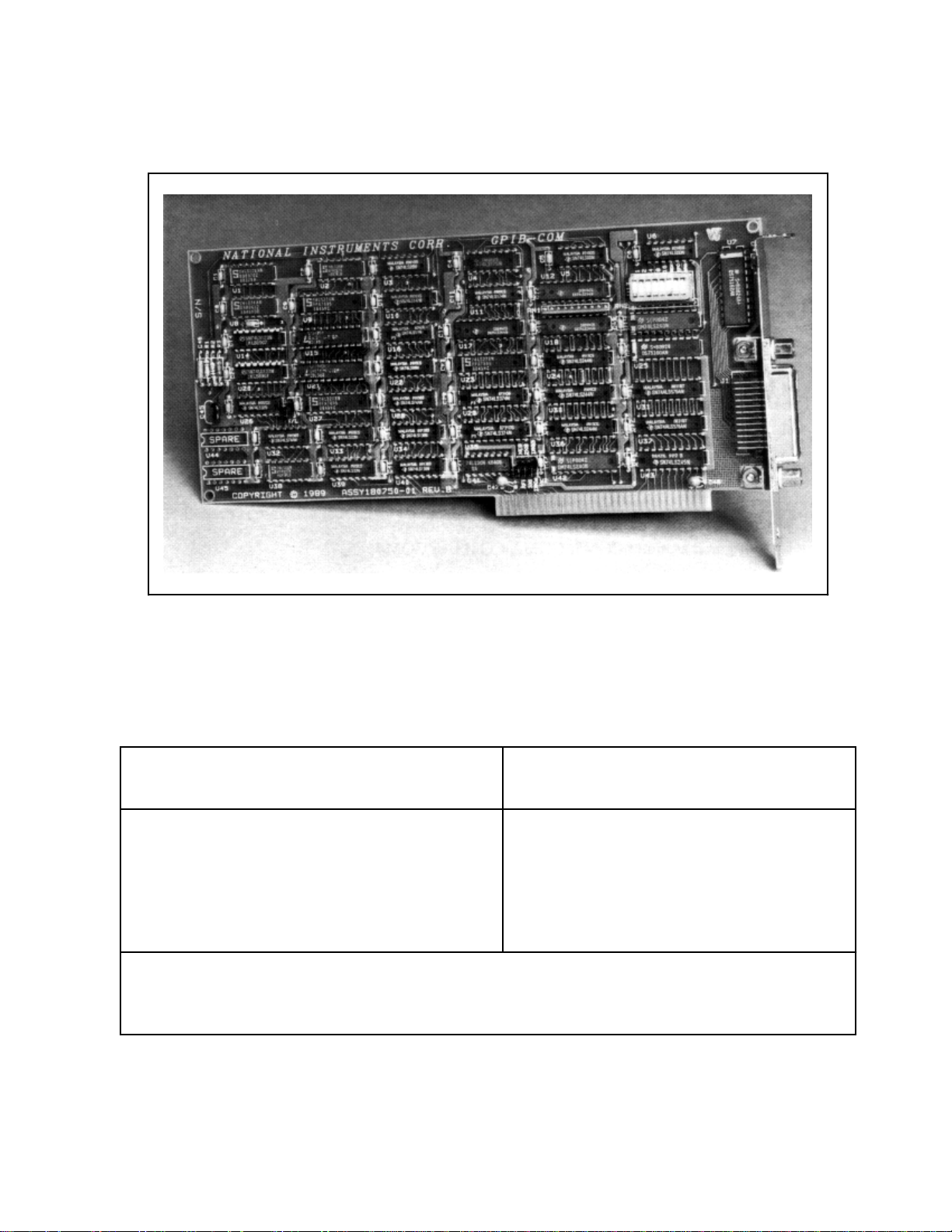
Figure 1-1 shows the GPIB-COM interface board.
Figure 1-1. GPIB-COM Board
What Your Kit Should Contain
Your kit should contain the following components:
Item Part Number
GPIB-COM interface board 180750-01
GPIB-COM User Manual 320197-01
GPIB-COM Diagnostic Test Diskette 420212-45
Note: The GPIB-COM Diagnostic Test Diskette contains the com.exe diagnostic test
that is described in Section Four, Running Diagnostic Tests.
Make sure each of these items is in your kit. If any item is missing, contact National Instruments.
GPIB-COM User Manual 1-2 © National Instruments Corporation
Page 12

Section One Introduction
Optional Equipment
Item Part Number
Double-Shielded Cables:
GPIB Type X2 Cable - 1 m 763061-01
GPIB Type X2 Cable - 2 m 763061-02
GPIB Type X2 Cable - 4 m 763061-03
* In order to meet FCC emission limits for a Class B device, you must use a shielded
GPIB cable. Operating this equipment with a non-shielded cable may cause interference
to radio and television reception in residential areas.
© National Instruments Corporation 1-3 GPIB-COM User Manual
Page 13
Section Two Configuration and Installation
This section contains information on how to configure and install the GPIB-COM into your
system.
Configuration
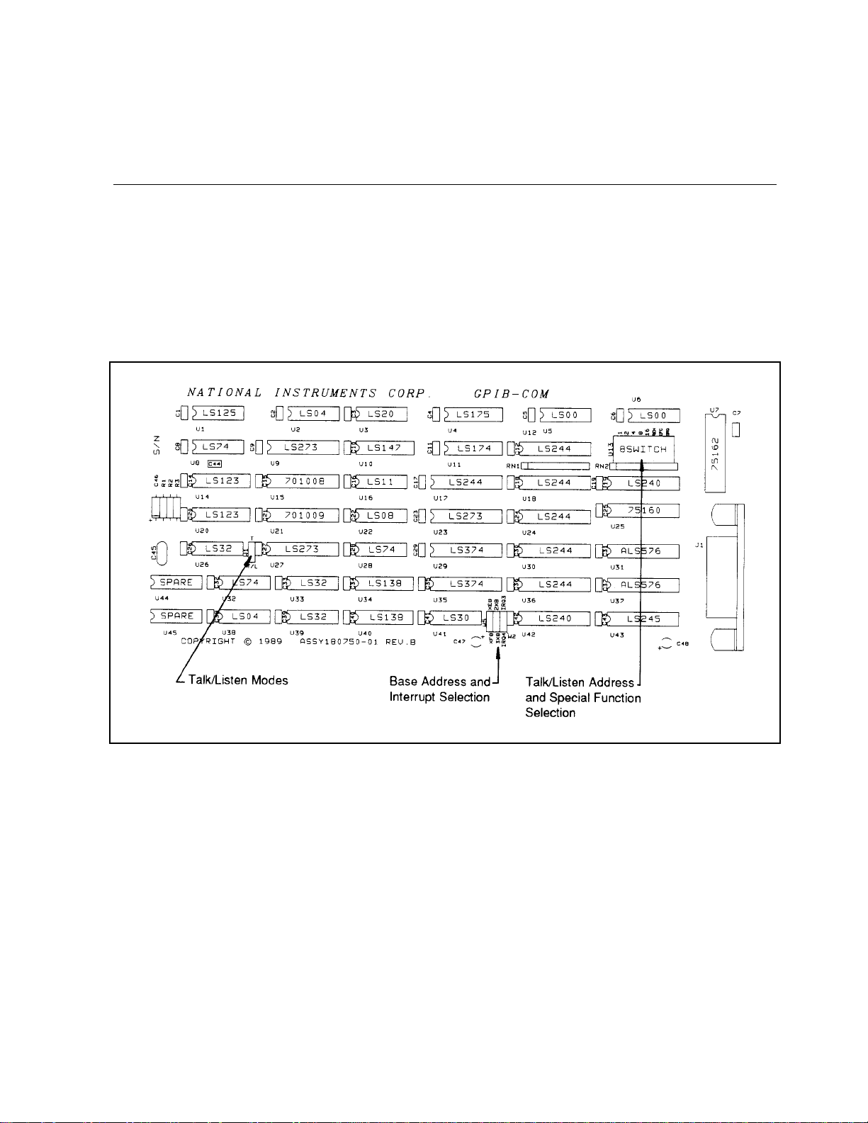
Figure 2-1 shows the locations of the GPIB-COM configuration jumpers and switches.
Figure 2-1. GPIB-COM Parts Locator Diagram
© National Instruments Corporation 2-1 GPIB-COM User Manual
Page 14

Configuration and Installation Section Two
When installing the GPIB-COM you must determine which serial port the GPIB-COM board will
respond to and select the appropriate base address and interrupt level. The GPIB-COM can be
configured to one of four base addresses:
• 3F8 for Serial Port 1
• 2F8 for Serial Port 2
• 3E8 for Serial Port 3
• 2E8 for Serial Port 4
Note: DOS and BIOS only recognize base addresses 3F8 and 2F8.
The GPIB-COM is shipped from the factory set to 3F8. It must be reconfigured to another base
address if another device (such as a printer adapter card or a built-in serial port) is already at that
address.
DOS has reserved device names for the serial ports it finds in the system: COM1 and COM2.
The serial port adapters are named in the order in which they are found. When the computer is
powered on, DOS searches the serial port addresses for installed adapters. It first searches 3F8,
then 2F8. If only one device is installed, that device is named COM1 regardless of what its I/O
address is. If there is more than one serial device installed, the first one found is assigned COM1
and the second one found is assigned COM2.
Some communications software also recognizes COM3 (base address 3E8) and COM4 (base
address 2E8). If you wish to use COM3 or COM4, set the jumpers to the desired base address as
shown in Figure 2-2. DOS and BIOS do not recognize COM3 or COM4. Consult your software
documentation to see which interrupt level, if any, is required. If interrupts are not used, the
jumper can be removed or stored with only one side on a pin.
The GPIB-COM may need to be reconfigured if its interrupt level conflicts with another device. If
the base I/O address of the GPIB-COM does not conflict with any other device in your computer
and the GPIB-COM still does not work with your software package, reconfigure the GPIB-COM
to a different interrupt level.
GPIB-COM User Manual 2-2 © National Instruments Corporation
Page 15

Section Two Configuration and Installation
Table 2-1 shows the standard base I/O address and interrupt level for each serial port.
Table 2-1. IBM PC Serial Port Adapters
Name of Port Base I/O Address (hex) Interrupt Level
Serial Port 1 3F8 4
Serial Port 2 2F8 3
Serial Port 3 3E8 Not Used
Serial Port 4 2E8 Not Used
Switch and Jumper Settings
Table 2-2 shows the factory settings and optional configurations for the switches and jumpers on
the GPIB-COM.
Table 2-2. Factory Default Settings and Optional Configurations
GPIB-COM Default Optional
Base I/O Address 3F8 2F8, 3E8, 2E8
Interrupt Level 4 3
If you need to change the factory settings, continue on. If you do not need to change the factory
settings, skip to Installation later in this section.
Base I/O Address and Interrupt Selection
The base I/O address and interrupt line used by the GPIB-COM are determined by the jumpers
located at positions W2 and W5. The jumpers are set at the factory for base I/O address 3F8 hex
and interrupt level 4.
© National Instruments Corporation 2-3 GPIB-COM User Manual
Page 16
Configuration and Installation Section Two
s
Figure 2-2 shows the four possible combinations of jumper settings.
W5
XF8
3X8
IRQ4
W2
a. COM1: Jumpers Set to Base I/O Address
3F8 hex and Interrupt Level 4 (Default)
XF8
•
3X8
IRQ4
W2
c. COM3: Jumpers Set to Base I/O Address
3E8 hex (Interrupts Not Used)
•
•
W5
•
• •
XE8
2X8
•
IRQ3
XE8
2X8
•
IRQ3
W5
XF8
3X8
IRQ4
•
W2
b. COM2: Jumpers Set to Base I/O Address
2F8 hex and Interrupt Level 3
XF8
•
3X8
IRQ4
W2
d. COM4: Jumpers Set to Base I/O Addres
2E8 hex (Interrupts Not Used)
•
•
W5
•
•
XE8
2X8
IRQ3
XE8
2X8
IRQ3
Figure 2-2. Possible Settings for GPIB-COM Jumpers
Talk/Listen Modes
If you are using your GPIB-COM with a listen-only printer or plotter, you can configure the
GPIB-COM for a talk-only mode. In this mode, the GPIB-COM is always a Talker and never
sends any interface commands. To set the talk-only mode, change jumper W1 from T/L to T as
shown in Figure 2-3:
W1
T/L
•
a. Talk/Listen
(Default)
T
T/L
Figure 2-3. Jumper W1 Settings
GPIB-COM User Manual 2-4 © National Instruments Corporation
W1
T
•
b. Talk Only
Page 17
Section Two Configuration and Installation
Talk/Listen Address and Special Function Selection
The GPIB-COM interface board has eight onboard DIP switches you can use to configure the
GPIB controller responsibilities. In the talk/listen mode, the first five switches set the talk or listen
address of the external device(s) that will be attached to the GPIB-COM. In the talk-only mode,
the GPIB-COM does not send a talk or listen address.
The three remaining switches (REN, IFC, and SRQ) have the following special functions:
Note: An asterisk (*) after a signal name indicates that the signal is inverted (negative logic).
REN* Asserts/unasserts the Remote Enable (REN) line that places an instrument in remote
mode. The ON position enables REN. The OFF position disables REN.
IFC* Enables/disables the Interface Clear (IFC) option on the GPIB-COM. If enabled, the
GPIB-COM issues an IFC when it is initialized. The ON position enables IFC on
initialization. The OFF position holds IFC unasserted.
SRQ* Enables/disables the Service Request (SRQ) option. If enabled, the GPIB-COM
monitors the SRQ line through the Parity Error Bit (PE) in the Line Status Register.
When the switch is ON, the PE bit reflects the status of the SRQ line. When the
switch is OFF, the PE bit is always clear.
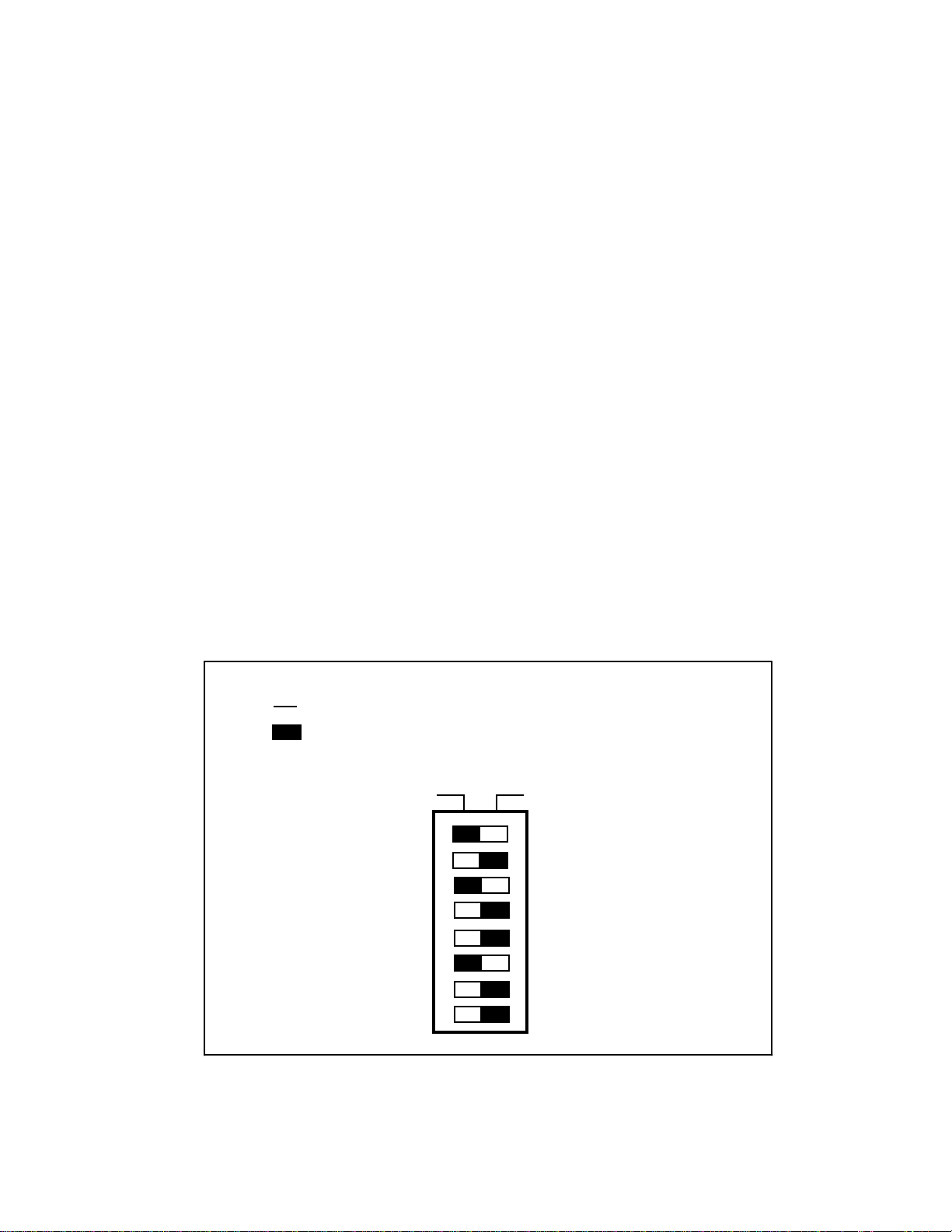
The GPIB-COM factory default switch configuration is for device listen address 5, REN* not
asserted, IFC* enabled, and SRQ* enabled. Figure 2-4 shows the factory default switch settings
for the GPIB-COM.
Key
= side you must press down for default setting; Off = 1; On =
12345678
This side down for logic 0This side down for logic 1
1
2
4
8
16
REN
IFC
SRQ
U13
OFF
Figure 2-4. Switch Setting for REN* OFF, IFC* ON, SRQ* ON, and Listen Address 5
(Default Setting)
© National Instruments Corporation 2-5 GPIB-COM User Manual
Page 18

Configuration and Installation Section Two
Figure 2-5 shows the switch configuration needed when using a device with listen address 10 hex.
The listen address varies with each device so check the listen address of your device and set these
five bits accordingly.
Key
= side you must press down for Listen Address 10;
Off = 1; On = 0
= used for setting REN* ON, IFC* ON, and SRQ* ON
This side down for logic 1
U13
OFF
This side down for logic 0
1
1
23 45 67 8
2
4
8
16
REN
IFC
SRQ
Figure 2-5. Listen Address Setting for Listen Address 10 Hex
GPIB-COM User Manual 2-6 © National Instruments Corporation
Page 19

Section Two Configuration and Installation
Figure 2-6 shows the switch configuration for REN* asserted, IFC* disabled, and SRQ* disabled.
Key
= side you must press down for REN* ON, IFC* OFF, and
SRQ* OFF; Off = 1; On = 0.
= used for setting Listen Address
This side down for logic 1 This side down for logic 0
OFF
U13
12 3 45 678
1
2
4
8
16
REN
IFC
SRQ
Figure 2-6. Switch Setting for REN* ON, IFC* OFF, and SRQ* OFF
Installation
Once you have changed, verified, and recorded the switches and jumper settings, you are ready to
install the GPIB-COM.
The following steps are general installation instructions. Consult the user manual or technical
reference manual of your personal computer for specific instructions and warnings.
1. Turn off your computer.
2. Remove the plug from its power source.
3. Remove the top cover or access port to the I/O channel.
4. Remove the expansion slot cover on the back panel of your computer.
5. Insert the GPIB-COM in an unused full-length slot with the IEEE-488 receptacle sticking out
of the opening of the back panel. It may be a tight fit, but do not force the board into place.
6. Screw the right angle mounting bracket of the GPIB-COM to the back panel rail of your
computer.
© National Instruments Corporation 2-7 GPIB-COM User Manual
Page 20

Configuration and Installation Section Two
7. Check the installation.
8. Replace the expansion slot cover of your computer.
9. Connect the GPIB cable to the GPIB-COM.
Special Considerations When Using the GPIB-COM
The GPIB-COM does not support XON/XOFF protocols. If your application software uses
XON/XOFF protocols, send your printer and plotter output to a file on disk. From DOS, send
your file to the GPIB-COM by using the DOS command:
copy
copy
The DOS MODE command is used to set the RS-232 parameters that will be used when COM1
and COM2 are accessed through DOS. Sometimes a timeout error may occur when writing
through the GPIB-COM to a slow device such as a printer or a plotter. If this happens, use the
MODE command to disable the timeout function by typing MODE COM1:12,,,,P. Some
software applications use the COM port baud rate setting to control the data transmission speed.
To obtain the fastest possible transfer rates, set the baud rate setting to 9600 baud. The P at the end
disables the timeout. For more information on the MODE command, refer to the IBM Disk
Operating System Manual. This command can also be used in an autoexec.bat file to disable
timeouts when you start up the computer.
filename
filename
COM1:
COM2:
GPIB-COM User Manual 2-8 © National Instruments Corporation
Page 21

Section Three Function Description
This section contains a block diagram of the GPIB-COM, followed by a description of each of its
functional components.
The GPIB-COM Interface
The GPIB-COM is a completely transparent interface between GPIB devices and any IBM PC
software that uses serial ports. A set of I/O registers identical to those on the standard IBM serial
adapter is used. On the GPIB side, the GPIB-COM includes a limited subset of interface
functions that address a GPIB device to listen when the computer sends data to the serial port and
to talk when the computer is waiting to receive data from the serial port. In order to be able to
respond immediately to commands and data sent to the serial port, the GPIB-COM must be the
GPIB System Controller and cannot work with other Controllers present.
© National Instruments Corporation 3-1 GPIB-COM User Manual
Page 22

Function Description Section Three
n
n
Figure 3-1 shows a block diagram of the GPIB-COM.
IRQ3
IRQ4
Config.
Jumpers
Interrupt
Control
Address Bus
AEN
IOW*
PC I/O Channel
IOR*
Data Bus
Config.
Jumpers
Directio
Buffer
Acceptor
Handshake
Mode Control
Logic
Address
Decoding
Source
Handshake
INS8250A
Compatible
Registers
Directio
Buffer
GPIB
Transceivers
GPIB
Figure 3-1. Block Diagram of GPIB-COM
GPIB-COM User Manual 3-2 © National Instruments Corporation
Page 23

Section Three Function Description
GPIB-COM Components
The interface consists of the following functional components:
• Address Decoding
• Configuration Jumpers
• INS8250A Compatible Registers
• GPIB Acceptor and Source Handshaking
• Mode Control Logic
• Interrupt Control Logic
• Direction Buffers
• GPIB Transceivers
Address Decoding
Address decoding monitors the PC address bus to recognize when a GPIB-COM address is
present and enables a read and/or write to its registers.
Configuration Jumpers
These onboard jumpers select the base address, GPIB controller mode, and interrupt request line
used by the GPIB-COM.
INS8250A Compatible Registers
The main component of an IBM PC compatible serial adapter is an INS8250A Asynchronous
Communications chip or its equivalent, which handles RS-232 communication. The INS8250A
compatible registers on the GPIB-COM emulate the serial adapter registers so that the GPIBCOM will operate transparently with any serial port driver.
GPIB Acceptor and Source Handshaking
This circuitry converts PC serial port handshaking into GPIB handshaking. This process is
completely software-transparent.
Mode Control Logic
This circuitry determines whether the GPIB-COM should be a Talker (and the target device a
Listener) or a Listener (and the target device a Talker).
Interrupt Control Logic
This circuitry generates and masks interrupts on GPIB conditions which correspond to the
conditions that would cause the INS8250A circuit to generate an interrupt.
© National Instruments Corporation 3-3 GPIB-COM User Manual
Page 24

Function Description Section Three
Direction Buffers
These buffers control the direction in which data information travels.
GPIB Transceivers
The GPIB-COM is interfaced to the IEEE-488 bus by National Semiconductor 75160A and
75162A transceivers. These integrated circuits are specifically designed to provide powerup/power-down bus protection (glitch-free). The GPIB-COM counts as one IEEE-488 bus load,
thereby allowing an additional 14 devices to be connected before exceeding the bus loading
restrictions imposed by the IEEE-488.
GPIB-COM User Manual 3-4 © National Instruments Corporation
Page 25

Section Four Running Diagnostic Tests
The GPIB-COM Test Commands
The GPIB-COM Diagnostic Tests can be used to verify the configuration of the GPIB-COM and
its connection to a GPIB printer or plotter.
To run a GPIB-COM diagnostic test, connect a printer or plotter to the GPIB and run the program
com.exe from the GPIB-COM diagnostic test diskette. The following message will appear on the
screen:
NATIONAL INSTRUMENTS GPIB-COM DIAGNOSTIC TESTS
This program assumes the GPIB-COM is configured at base address
3F8 (COM1).
If you reconfigured your GPIB-COM you must change the address
that this program uses. To do this, enter command c from the
menu.
Enter one of the following commands:
-1 printer test
-2 plotter test
-c change COM configuration
-q quit
?
A short explanation of each command is given in the following paragraphs.
-1 printer test
Select this test to verify the configuration of the GPIB-COM when connecting it to a GPIB ASCII
printer. This test will send characters to the printer.
Entering this command returns the prompt:
Starting printer test.
Press any key to stop printing.
© National Instruments Corporation 4-1 GPIB-COM User Manual
Page 26

Running Diagnostic Tests Section Four
The printer should begin printing a string of characters. To stop the test, press any key. The
following message then appears:
Printer test finished.
Please check output to printer with user manual instructions.
The output on the printer should read:
NATIONAL INSTRUMENTS GPIB-COM DIAGNOSTIC TEST!"#$%&'()*+,-.
/0123456789:;<=>?@ABCDEFGHIJKLMNOPQRSTUVWXYZ[\]_'abcdefghijkl
mnopqrstuvwxyz{|}~ !"#$%&'()*+,./0123456789:;<=>?@ABCDEFGHI
JKLMNOPQRSTUVWXY Z[\]_'abcdefghijklmnopqrstuvwxyz{|}~ !"#$%&'
()*+,./0123456789:;<=>?@ABCDEFGHIJKLMNOPQRSTUVWXYZ[\]_'abcdefghi
jklmnopqrstuvwxyz{|}~ !"#$%&'()*+,./0123456789:;<=>?@ABCDEFG
HIJKLMNOPQRSTUVWXYZ[\]_'abcdefghijklmnopqrstuvwxyz{|}~
If the printer does not respond, an error message appears on the screen along with a message
telling you to recheck all of your connections and jumper settings. If the test still fails after
everything has been checked, write down the error message, if any, and call National Instruments.
-2 plotter test
Select this test to verify the configuration of the GPIB-COM when connecting it to a GPIB HP-GL
plotter. This test will send output to the plotter.
When this command is selected, the computer prints the following message:
Starting plotter test.
As illustrated in Figure 4-1, the plotter begins to draw four ovals.
Figure 4-1. Plotter Output
GPIB-COM User Manual 4-2 © National Instruments Corporation
Page 27

Section Four Running Diagnostic Tests
When it is finished, the following message appears on the screen:
Plotter test finished.
Please check output to plotter with user manual instructions.
If the plotter does not respond or the output on the plotter does not match Figure 4-1, check again
to be sure that all of the connections are tight and the jumpers are all set correctly. Try the test
again. If it still does not work, write down any error messages that appear and call National
Instruments.
-c change COM configuration
This command is used to change the base address of the GPIB-COM to match the actual board
settings. If you have changed the jumper settings to something different than the default settings,
you must run this command.
When this command is selected, the following menu appears:
This program assumes the GPIB-COM is configured at base address
3F8 (COM1).
Enter the number of the correct address.
1) base address 3F8 (COM1)
2) base address 2F8 (COM2)
Enter 1, 2, or <return> for no change?
Type in the number of the address that you have configured the board to. The computer prints out
your choice and returns to the main menu.
-q quit
This command ends the test program and returns to DOS.
© National Instruments Corporation 4-3 GPIB-COM User Manual
Page 28

Section Five Programming the GPIB-COM
This section presents a description of the GPIB-COM Serial Port Emulator registers and
information on programming the GPIB-COM. You need to use this section only if you are
writing your own serial port device driver.
The GPIB-COM Registers
IBM's serial adapter is a plug-in card for the PC that handles RS-232 communication. The main
component of the adapter is an INS8250 Asynchronous Communications chip or its equivalent,
which is controlled by programming a set of registers on the I/O channel. The names of these
registers and their I/O addresses are given in Table 5-1. Each register is located at a certain offset
from the base address of the board. The addresses are given with an X for the first digit and a Y
for the second digit, where XY=3F for COM1 (base address 3F8), XY=2F for COM2 (base
address 2F8), XY=3E for COM3 (base address 3E8), and XY=2E for COM4 (base address
2E8). Notice that sometimes two registers share the same I/O address. The DLAB bit (bit 7 of
the Line Control Register) determines which register will respond when these addresses are
accessed.
Note: Throughout this section, the term set will be used to mean that a bit is a logical 1, and clear
will mean that the bit is a logical 0.
Table 5-1. GPIB-COM Registers
I/O Address Offset from
Register Type XY=3F for COM1 Base Address
XY=2F for COM2
XY=3E for COM3
XY=2E for COM4
Transmitter Holding Register write XY8 (DLAB=0) 0
Receive Buffer Register read XY8 (DLAB=0) 0
Divisor Latch LSB Register read/write XY8 (DLAB=1) 0
Divisor Latch MSB Register read/write XY9 (DLAB=1) 1
Interrupt Enable Register read/write XY9 (DLAB=0) 1
Interrupt Identification Register read XYA 2
Line Control Register read/write XYB 3
Modem Control Register read/write XYC 4
Line Status Register read XYD 5
Modem Status Register read XYE 6
The following pages describe the functions of each register on the serial adapter and on the GPIBCOM. For a more complete description of the serial adapter, refer to the IBM Options and
Adapters Manual.
© National Instruments Corporation 5-1 GPIB-COM User Manual
Page 29

Programming the GPIB-COM Section Five
Transmitter Holding Register
Offset from Base I/O Address = 0
Register Address = XF8
DLAB bit in Line Control Register = 0
7 654 321
D7
D6 D5
D4
D3
D2 D1 D0
0
W
The Transmitter Holding Register contains the character to be sent to the serial output, with bit 0
being the least significant and bit 7 the most significant. It functions identically on the GPIB-COM
and the INS8250.
Bit Mnemonic Description
7-0w D[7-0] Data Bits 7 through 0
GPIB-COM User Manual 5-2 © National Instruments Corporation
Page 30

Section Five Programming the GPIB-COM
Receive Buffer Register
Offset from Base I/O Address = 0
Register Address = XF8
DLAB bit in Line Control Register = 0
7 654 321
D7
D6 D5
D4
D3
D2 D1 D0
0
R
The Receive Buffer Register contains the character received from the serial input, with bit 0 being
the least significant and bit 7 the most significant. It functions identically on the GPIB-COM and
the INS8250.
Bit Mnemonic Description
7-0r D[7-0] Data Bits 7 through 0
© National Instruments Corporation 5-3 GPIB-COM User Manual
Page 31

Programming the GPIB-COM Section Five
Divisor Latch Least Significant Byte (LSB) Register
Offset from Base I/O Address = 0
Register Address = XF8
DLAB bit in Line Control Register = 1
7 654 321
DL7
DL6 DL5
DL4
DL3
DL2 DL1 DL0 R/W
Bit Mnemonic Description
7-0r/w DL[7-0] Data Bits 7 through 0
Divisor Latch Most Significant Byte (MSB) Register
Offset from Base I/O Address = 1
Register Address = XF9
DLAB bit in Line Control Register = 1
7 654 321
DL15
DL14 DL13
DL12
DL11
DL10 DL9 DL8 R/W
0
0
The value stored in these two registers is used to determine the baud rate for serial communications. The 16-bit number formed by the Divisor Latch LSB and MSB is divided into a 1.8432
MHz clock to produce the baud rate.
The Divisor Latch Registers are ignored by the GPIB-COM circuitry; however, they are available
on the GPIB-COM and can be written to and read by software.
Bit Mnemonic Description
7-0r/w DL[15-8] Data Bits 15 through 8
GPIB-COM User Manual 5-4 © National Instruments Corporation
Page 32

Section Five Programming the GPIB-COM
Interrupt Enable Register
Offset from Base I/O Address = 1
Register Address = XF9
DLAB bit in Line Control Register = 0
7 654 321
0
00
0
MS
RLS THR RDA
0
R/W
The Interrupt Enable Register is a read/write register that allows the programmer to selectively
enable or disable each of the four possible types of interrupts generated by the INS8250. The high
four bits are not used and are permanently cleared. The lower four bits each enable one type of
interrupt as listed below.
Bit Mnemonic Description
7-4r/w 0 Reserved Bits 7 through 4
These bits always read as 0.
3r/w MS Modem Status Interrupt Enable Bit
This bit enables a modem status interrupt when set to logical 1.
The modem status interrupt occurs when any of bits 0 through 3
of the Modem Status Register are set to logical 1.
This bit is identical on the GPIB-COM and the INS8250, but
bits 0 through 3 of the Modem Status Register are set for
different conditions as noted under the Modem Status Register
description.
2r/w RLS Receive Line Status Interrupt Enable Bit
This bit enables a line status interrupt when set. The line status
interrupt occurs when any of bits 1 through 4 of the Line Status
Register become set.
This bit is identical on the GPIB-COM and the INS8250, but
bits 1 through 4 of the Line Status Register are set for different
conditions as noted under the Line Status Register description.
© National Instruments Corporation 5-5 GPIB-COM User Manual
Page 33

Programming the GPIB-COM Section Five
Bit Mnemonic Description
1r/w THR Transmitter Holding Register Interrupt Enable Bit
This bit enables a transmitter holding register empty interrupt
when set. The transmitter holding register empty interrupt
occurs when the INS8250 becomes ready to send another
character.
This bit functions identically on the GPIB-COM and the
INS8250.
0r/w RDA Received Data Available Interrupt Enable Bit
This bit enables a received data available interrupt when set. The
received data available interrupt occurs when a character is
received from the serial input and stored in the Receive Buffer
Register.
This bit functions identically on the GPIB-COM and the
INS8250.
GPIB-COM User Manual 5-6 © National Instruments Corporation
Page 34

Section Five Programming the GPIB-COM
Interrupt Identification Register
Offset from Base I/O Address = 2
Register Address = XFA
7 654 321
0
00
0
0
ID1 ID0 INT
0
R
The Interrupt Identification Register is a read-only register which tells you when an interrupt is
pending and if so, what kind of interrupt it is. This register functions identically on the GPIBCOM and the INS8250.
Bit Mnemonic Description
7-3r 0 Reserved Bits 7 through 3
These bits always read as 0.
2-1r ID[1-0] Identify Interrupt Register Bits
These two bits identify the interrupt that is pending. If more
than one interrupt is pending, only the one with the highest
priority is identified. The types and priorities are given in Table
5-2.
Table 5-2. Interrupt Types and Priorities
Bit 2 Bit 1 Type of Interrupt Priority
0 0 Receiver Line Status 1st
0 1 Received Data Available 2nd
1 0 Transmitter Holding
Register Empty 3rd
1 1 Modem Status 4th
0r INT Interrupt Pending Bit
This bit is clear if an interrupt is pending. If set, no interrupt is
pending.
© National Instruments Corporation 5-7 GPIB-COM User Manual
Page 35

Programming the GPIB-COM Section Five
Line Control Register
Offset from Base I/O Address = 3
Register Address = XFB
7 654 321
SBRK STPDLAB EVEN
PEN
STB WL1 WL0 R/W
0
The Line Control Register is a read/write register that allows the programmer to set the RS-232
parameters for the INS8250. The function of each bit in this register is explained below.
Bit Mnemonic Description
7r/w DLAB Divisor Latch Access Bit
This bit controls which registers will respond to I/O addresses
XF8 and XF9. This bit is set to access the Divisor Latch LSB
and MSB, and cleared to access the Transmitter Holding
Register, the Receive Buffer Register, and the Interrupt Enable
Register.
This bit functions identically on the GPIB-COM and the
INS8250.
6r/w SBRK Set Break Control Bit
When set, this bit causes the SOUT line of the serial cable to be
forced to a logical 0 state.
This bit is ignored by the GPIB-COM.
5r/w STP Stick Parity Bit
When this bit is set, the parity bit transmitted and detected will
be the inverse of the EVEN bit (bit 4), regardless of the number
of 1's in the data word.
This bit is ignored by the GPIB-COM.
4r/w EVEN Even Parity Select Bit
If this bit is set, even parity will be generated and checked. If
this bit is clear, odd parity will be generated and checked.
This bit is ignored by the GPIB-COM.
GPIB-COM User Manual 5-8 © National Instruments Corporation
Page 36

Section Five Programming the GPIB-COM
Bit Mnemonic Description
3r/w PEN Parity Enable Bit
If this bit is set, the INS8250 will generate and check parity
according to the values of the STP and EVEN bits (bits 4 and
5). If this bit is clear, the INS8250 will not generate or check
parity bits.
This bit is ignored by the GPIB-COM.
2r/w STB Stop Bit Control Bit
This bit controls the number of stop bits sent and verified by the
INS8250. If this bit is set, two stop bits will be used. If this bit
is clear, one stop bit will be used.
This bit is ignored by the GPIB-COM.
1-0r/w WL[1-0] Word Length Select Bits
These two bits set the length of the words sent or received
according to Table 5-3.
Table 5-3. Word Length Select Bits
Bit 1 Bit 0 Word Length
0 0 5 bits
0 1 6 bits
1 0 7 bits
1 1 8 bits
These bits have no meaning on the GPIB and are ignored by the
GPIB-COM circuitry.
© National Instruments Corporation 5-9 GPIB-COM User Manual
Page 37

Programming the GPIB-COM Section Five
Modem Control Register
Offset from Base I/O Address = 4
Register Address = XFC
7 654 321
0
00
LOOP
OUT2
OUT1 RTS DTR
0
R/W
The Modem Control Register is a read/write register that controls RS-232 output lines for
communication with a modem or modem emulator. The function of each bit in this register is
explained below.
Bit Mnemonic Description
7-5r/w 0 Reserved Bits 7 through 5
These bits always read as 0.
4r/w LOOP Loopback Diagnostic Test Bit
When set, this bit internally connects the outputs of the INS8250
back to the inputs to allow the chip to be tested by writing data to
itself and reading it back for verification.
This bit is ignored by the GPIB-COM circuitry.
3r/w OUT2 Auxiliary Output 2 Bit
The OUT2 serial port output is the inverse of this bit. All
interrupts from the serial adapter are disabled when this bit is
cleared.
When this bit is cleared, interrupts are disabled on the GPIBCOM.
2r/w OUT1 Auxiliary Output 1 Bit
The OUT1 serial port output is the inverse of this bit.
This bit is ignored by the GPIB-COM circuitry.
1r/w RTS Request to Send Bit
The RTS serial port output is the inverse of this bit. When this
bit is set, it indicates that the Controller is ready to send data.
On the GPIB-COM, this bit is used along with the DTR bit to
control the CTS bit of the Modem Status Register.
GPIB-COM User Manual 5-10 © National Instruments Corporation
Page 38

Section Five Programming the GPIB-COM
Bit Mnemonic Description
0r/w DTR Data Terminal Ready Bit
The DTR serial port output is the inverse of this bit. This bit is
set when the Controller is ready to communicate.
On the GPIB-COM, this bit is used along with the RTS bit to
control the CTS bit of the Modem Status Register.
© National Instruments Corporation 5-11 GPIB-COM User Manual
Page 39

Programming the GPIB-COM Section Five
Line Status Register
Offset from Base I/O Address = 5
Register Address = XFD
7 654 321
0
TEMT THRE
BI
FE
PE OE DR
0
R
The Line Status Register provides information about the status of the data transfer. On the GPIBCOM this register is implemented as a read-only register. Writing to the line status register will
not change its contents. The function of each bit in this register is explained below.
Bit Mnemonic Description
7r 0 Reserved Bit
This bit always reads as 0.
6r TEMT Transmitter Shift Register Empty Bit
This bit is cleared when a character is transferred from the
Transmitter Holding Register to the Transmitter Shift Register
and set when the character has been shifted out of the Shift
Register onto the serial output line.
On the GPIB-COM, there is no shift register so this bit behaves
exactly the same as the THRE bit.
5r THRE Transmitter Holding Register Empty Bit
This bit is cleared when the processor writes a character into the
Transmitter Holding Register and set when the character has
been transmitted and the INS8250 is ready to send another
character.
This bit functions identically on the GPIB-COM and the
INS8250.
4r BI Break Interrupt Bit
This bit is set to logical 1 when the serial data input remains in
the logical 0 state for longer than one full word transmission
time.
On the GPIB-COM, this bit is always clear.
GPIB-COM User Manual 5-12 © National Instruments Corporation
Page 40

Section Five Programming the GPIB-COM
Bit Mnemonic Description
3r FE Framing Error Bit
This bit is set when the received character does not have a valid
stop bit.
On the GPIB-COM, this bit is always clear.
2r PE Parity Error Bit
This bit is set when the received character does not have the
correct parity. It is cleared when the processor reads the Line
Status Register.
On the GPIB-COM, this bit is set when the SRQ* line of the
GPIB is asserted. When the special function selection DIP
switch has been set to disable the SRQ feature, this bit is always
clear.
1r OE Overrun Error Bit
This bit is set when a new character is received and stored in the
Receive Buffer Register before the processor reads the previous
character, thus overwriting and destroying the previous
character. It is cleared when the processor reads the Line Status
Register.
On the GPIB-COM, this bit is always clear.
0r DR Data Ready Bit
This bit is set when a character has been received and stored in
the Receive Buffer Register. It is cleared when the processor
reads the Receive Buffer Register.
This bit functions identically on the GPIB-COM and the
INS8250.
© National Instruments Corporation 5-13 GPIB-COM User Manual
Page 41

Programming the GPIB-COM Section Five
Modem Status Register
Offset from Base I/O Address = 6
Register Address = XFE
7 654 321
RI DSRDCD CTS DDCD TERI DDSR DCTS
0
R
The Modem Status Register gives the state of the modem control lines and tells whether any of
these lines have changed state since the register was last read. This register is read only on the
GPIB-COM. Writing to this register will not change its contents. The function of each bit in this
register is explained below.
Bit Mnemonic Description
7r DCD Data Carrier Detect Bit
This bit reflects the inverse of the serial port DCD input signal.
On the GPIB-COM, this bit is always clear.
6r RI Ring Indicator Bit
This bit reflects the inverse of the serial port RI input signal.
On the GPIB-COM, this bit is always clear.
5r DSR Data Set Ready Bit
This bit reflects the inverse of the serial port DSR input signal.
On the GPIB-COM, this bit is always set to indicate that the
interface is ready to transfer data.
4r CTS Clear to Send Bit
This bit reflects the inverse of the serial port CTS input signal.
On the GPIB-COM, this bit is the logical AND of the DTR and
RTS bits of the Modem Control Register.
3r DDCD Delta Data Carrier Detect Bit
This bit is set when the serial port DCD input signal changes
state and cleared when the processor reads the Modem Status
Register.
On the GPIB-COM, this bit is always clear.
GPIB-COM User Manual 5-14 © National Instruments Corporation
Page 42

Section Five Programming the GPIB-COM
Bit Mnemonic Description
2r TERI Trailing Edge Ring Indicator Bit
This bit is set when the serial port RI input signal changes from
a logical 1 to a logical 0 and cleared when the processor reads
the Modem Status Register.
On the GPIB-COM, this bit is always clear.
1r DDSR Delta Set Ready Bit
This bit is set when the serial port DSR input signal changes
state and cleared when the processor reads the Modem Status
Register.
On the GPIB-COM, this bit is always clear.
0r DCTS Delta Clear to Send Bit
This bit is set when the CTS input changes state and cleared
when the processor reads the Modem Status Register.
On the GPIB-COM, this bit is the logical AND of the DTR and
RTS bits of the Modem Control Register.
© National Instruments Corporation 5-15 GPIB-COM User Manual
Page 43

Programming the GPIB-COM Section Five
Programming the Serial Adapter
The operation of the serial adapter is controlled by software, either IBM BIOS or an application.
To transfer data to and from the serial port, the communications parameters must first be set up in
the following manner:
1. Load the baud rate divisor into the divisor latch.
2. Store the RS-232 parameters in the Line Control Register.
3. Send the modem control signals by writing to the Modem Control Register.
4. Enable interrupts, if used, by writing to the appropriate bits in the Interrupt Enable Register.
Once the control registers have been programmed correctly, the software can transmit and receive
serial data by polling, interrupts, or both.
Polling Method
In the polled method of operation, the Line Status Register is continuously read to check if the Data
Ready Bit is set. When this bit becomes set, the Receive Buffer Register is read to get the
character that just came from the serial port, and the process continues. To transmit data, the Line
Status Register is polled until the Transmitter Holding Register Empty Bit is set. A byte can then
be written to the Transmitter Holding Register, and polling continues.
Interrupt-Driven Method
In the interrupt-driven mode of operation, the desired interrupts are enabled through the OUT2 bit
and the Interrupt Enable Register. An interrupt handler is installed to respond when an interrupt
occurs. Software processes can perform other tasks until an interrupt is received. When an
interrupt occurs, the handler reads the Interrupt Identification Register to determine the type of
interrupt and takes appropriate action, such as reading the Receive Buffer Register in the case of a
received data available interrupt, writing to the Transmitter Holding Register if it was a THRE
interrupt, or printing an error message in the case of a line status interrupt.
GPIB-COM User Manual 5-16 © National Instruments Corporation
Page 44

Section Five Programming the GPIB-COM
The GPIB-COM Controller Function
Because most serial port applications involve communication with only one serial line, the GPIBCOM imposes some restrictions on the GPIB in order to be compatible with existing serial port
software. The GPIB-COM must be System Controller of the GPIB and will not work with other
Controllers. The behavior of the GPIB-COM depends on the setting of the talk-only jumper.
If the jumper is set to talk-only, the GPIB-COM assumes that there is a listen-only device
connected to the GPIB. When a byte is written into the Transmitter Holding Register, the GPIBCOM sets the THRE bit of the Line Status Register to 0, puts the contents of that register on the
GPIB data lines, and begins the source handshake sequence. When the Listener releases NDAC*,
the THRE bit is set back to 1 and the GPIB-COM waits for another byte to be written into the
Transmitter Holding Register.
If the jumper is set to talk/listen, the GPIB-COM assumes that the device connected to the GPIB
can be addressed to listen or talk. When the computer is powered on, the GPIB-COM sends the
talk address that is set on the DIP switches, addresses itself as a Listener, and unasserts NRFD*.
If the GPIB device sends a byte, the GPIB-COM accepts it, stores it in the Receive Buffer
Register, and sets the DR bit of the Line Status Register. At the end of the GPIB handshake, it
keeps NRFD* asserted until the computer reads the byte from the Receive Buffer Register.
If the computer writes a byte to the Transmitter Holding Register, the GPIB-COM sends the GPIB
device its listen address from the DIP switches and addresses itself to talk. Then it sends the byte
to the GPIB device, which is now addressed as a Listener. When the GPIB-COM begins a source
handshake, it starts a 200-msec timer. If the source handshake is completed before the 200 msec
is expired, the GPIB-COM remains addressed to talk until the timer runs out. If the computer
writes another byte before the timer runs out, the GPIB-COM restarts the timer and sends the byte.
When 200 msec has passed since the last byte was written, the GPIB-COM sends the talk address
and addresses itself to listen again. If a byte was waiting in the Receive Buffer Register when the
computer wrote to the Transmitter Holding Register, the GPIB-COM remembers this and when it
becomes a Listener again, it asserts NRFD* until the computer reads the byte from the Receive
Buffer Register.
© National Instruments Corporation 5-17 GPIB-COM User Manual
Page 45

Appendix A Specifications
This appendix lists the specifications of the GPIB-COM board.
Power Requirement
+5 VDC (± 5%) 0.75 A typical
Physical
Dimensions 4.2 in. by 8.75 in.
I/O Connector IEEE-488 Standard 24-pin
Operating Environment
Component Temperature 0° to 70° C
Relative Humidity 5% to 90%, noncondensing
Emissions FCC Class B
Storage Environment
Temperature -55° to 125° C
Relative Humidity 5% to 90%, noncondensing
© National Instruments Corporation A-1 GPIB-COM User Manual
Page 46

Appendix B Multiline Interface Command Messages
The following tables are multiline interface messages (sent and received with ATN TRUE).
© National Instruments Corporation B-1 GPIB-COM User Manual
Page 47

Multiline Interface Command Messages Appendix B
Multiline Interface Messages
Hex Oct Dec ASCII Msg Hex Oct Dec ASCII Msg
00 000 0 NUL 20 040 32 SP MLA0
01 001 1 SOH GTL 21 041 33 ! MLA1
02 002 2 STX 22 042 34 " MLA2
03 003 3 ETX 23 043 35 # MLA3
04 004 4 EOT SDC 24 044 36 $ MLA4
05 005 5 E NQ PPC 25 045 37 % MLA5
06 006 6 ACK 26 046 38 & MLA6
07 007 7 BEL 27 047 39 ' MLA7
08 010 8 BS GET 28 050 40 ( MLA8
09 011 9 HT TCT 29 051 41 ) MLA9
0A 012 10 LF 2A 052 42 * MLA10
0B 013 11 VT 2B 053 43 + MLA11
0C 014 12 F F 2C 054 44 , MLA12
0D 015 13 CR 2D 055 45 - MLA13
0E 016 14 SO 2E 056 46 . MLA14
0F 017 15 SI 2F 057 47 / MLA15
10 020 16 DLE 30 060 48 0 MLA16
11 021 17 DC1 LLO 31 061 49 1 MLA17
12 022 18 DC2 32 062 50 2 MLA18
13 023 19 DC3 33 063 51 3 MLA19
14 024 20 DC4 DCL 34 064 52 4 MLA20
15 025 21 NAK PPU 35 065 53 5 MLA21
16 026 22 SYN 36 066 54 6 MLA22
17 027 23 ETB 37 067 55 7 MLA23
18 030 24 CAN SPE 38 070 56 8 MLA24
19 031 25 EM SPD 39 071 57 9 MLA25
1A 032 26 SUB 3A 072 58 : MLA26
1B 033 27 ESC 3B 073 59 ; MLA27
1C 034 28 FS 3C 074 60 < MLA28
1D 035 29 GS 3D 075 61 = MLA29
1E 036 30 RS 3E 076 62 > MLA30
1F 037 31 US 3F 077 63 ? UNL
Message Definitions
DCL Device Clear
GET Group Execute Trigger
GTL Go To Local
LLO Local Lockout
MLA My Listen Address
MSA My Secondary Address
MTA My Talk Address
PPC Parallel Poll Configure
PPD Parallel Poll Disable
GPIB-COM User Manual B-2 © National Instruments Corporation
Page 48

Appendix B Multiline Interface Command Messages
Multiline Interface Messages
Hex Oct Dec ASCII Msg Hex Oct Dec ASCII Msg
40 100 64 @ MTA0 60 140 96 ` MSA0,PPE
41 101 65 A MTA1 61 141 97 a MSA1,PPE
42 102 66 B MTA2 62 142 98 b MSA2,PPE
43 103 67 C MTA3 63 143 99 c MSA3,PPE
44 104 68 D MTA4 64 144 100 d MSA4,PPE
45 105 69 E MTA5 65 145 101 e MSA5,PPE
46 106 70 F MTA6 66 146 102 f MSA6,PPE
47 107 71 G MTA7 67 147 103 g MSA7,PPE
48 110 72 H MTA8 68 150 104 h MSA8,PPE
49 111 73 I MTA9 69 151 105 i MSA9,PPE
4A 112 74 J MTA10 6A 152 106 j MSA10,PPE
4B 113 75 K MTA11 6B 153 107 k MSA11,PPE
4C 114 76 L MTA12 6C 154 108 l MSA12,PPE
4D 115 77 M MTA13 6D 155 109 m MSA13,PPE
4E 116 78 N MTA14 6E 156 110 n MSA14,PPE
4F 117 79 O MTA15 6F 157 111 o MSA15,PPE
50 120 80 P MTA16 70 160 112 p MSA16,PPD
51 121 81 Q MTA17 71 161 113 q MSA17,PPD
52 122 82 R MTA18 72 162 114 r MSA18,PPD
53 123 83 S MTA19 73 163 115 s MSA19,PPD
54 124 84 T MTA20 74 164 116 t MSA20,PPD
55 125 85 U MTA21 75 165 117 u MSA21,PPD
56 126 86 V MTA22 76 166 118 v MSA22,PPD
57 127 87 W MTA23 77 167 119 w MSA23,PPD
58 130 88 X MTA24 78 170 120 x MSA24,PPD
59 131 89 Y MTA25 79 171 121 y MSA25,PPD
5A 132 90 Z MTA26 7A 172 122 z MSA26,PPD
5B 133 91 [ MTA27 7B 173 123 { MSA27,PPD
5C 134 92 \ MTA28 7C 174 124 | MSA28,PPD
5D 135 93 ] MTA29 7D 175 125 } MSA29,PPD
5E 136 94 ^ MTA30 7 E 176 126 ~ MSA30,PPD
5F 137 95 _ UNT 7F 177 127 DEL
PPE Parallel Poll Enable
PPU Parallel Poll Unconfigure
SDC Selected Device Clear
SPD Serial Poll Disable
SPE Serial Poll Enable
TCT Take Control
UNL Unlisten
UNT Untalk
© National Instruments Corporation B-3 GPIB-COM User Manual
Page 49

Appendix C Operation of the GPIB
History of the GPIB
The GPIB is a link, bus, or interface system through which interconnected electronic devices
communicate. Hewlett-Packard invented the GPIB, which they call the HP-IB, to connect and
control programmable instruments manufactured by them. Because of its high system data rate
ceilings of from 250 kbytes/sec to 1 Mbyte/sec, the GPIB quickly became popular in other
applications such as intercomputer communication and peripheral control. It was later accepted as
the industry standard IEEE-488. The versatility of the system prompted the name General
Purpose Interface Bus.
Types of Messages
Devices on the GPIB communicate by passing messages through the interface system. There are
two types of messages:
• Device-dependent messages, often called data or data messages, contain device-specific
information such as programming instructions, measurement results, machine status, and data
files.
• Interface messages manage the bus itself. They are usually called commands or command
messages. Interface messages perform such functions as initializing the bus, addressing and
unaddressing devices, and setting devices for remote or local programming.
Note: The term command as used here should not be confused with some device instructions
which are also called commands. Such device-specific instructions are actually data
messages.
Talkers, Listeners, and Controllers
There are three types of GPIB communicators. A Talker sends data messages to one or more
Listeners. The Controller manages the flow of information on the GPIB by sending commands to
all devices.
Devices can be Talkers, Listeners, and/or Controllers. A digital multimeter, for example, is a
Talker and may also be a Listener. A printer or plotter is usually only a Listener. A computer on
the GPIB often combines all three roles to manage the bus and communicate with other devices.
The GPIB is a bus like a typical computer bus except that the computer has its circuit cards
interconnected via a backplane bus whereas the GPIB has standalone devices interconnected via a
cable bus.
The role of the GPIB Controller can also be compared to the role of the computer's CPU, but a
better analogy is to the switching center of a city telephone system.
The switching center (Controller) monitors the communications network (GPIB). When the
center (Controller) notices that a party (device) wants to make a call (send a data message), it
connects the caller (Talker) to the receiver (Listener).
© National Instruments Corporation C-1 GPIB-COM User Manual
Page 50

Operation of the GPIB Appendix C
The Controller usually addresses a Talker and a Listener before the Talker can send its message to
the Listener. After the message is transmitted, the Controller usually unaddresses both devices.
Some bus configurations do not require a Controller. For example, one device may only be a
Talker (called a talk-only device) and there may be one or more listen-only devices.
A Controller is necessary when the active or addressed Talker or Listener must be changed. The
Controller function is usually handled by a computer.
System Controller and Active Controller
Although there can be multiple Controllers on the GPIB, only one Controller at a time is Active
Controller or Controller-in-Charge. Active control can be passed from the current Active
Controller to an idle Controller. Only one device on the bus, the System Controller, can make
itself the Active Controller.
GPIB Signals
The interface bus consists of 16 signal lines and 8 ground return or shield drain lines. The 16
signal lines are divided into three groups:
• eight data lines
• three handshake lines
• five interface management lines
GPIB-COM User Manual C-2 © National Instruments Corporation
Page 51

Appendix C Operation of the GPIB
Figure C-1 shows the arrangement of these signals on the GPIB cable connector.
13
DIO1*
DIO2*
DIO3*
DIO4*
EOI*
DAV*
NRFD*
NDAC*
IFC*
SRQ*
ATN*
SHIELD
1
2
3
4
5
6
7
8
9
10
11
12
DIO5*
14
DIO6*
15
DIO7*
16
DIO8*
17
REN*
18
GND (TW PAIR W/DAV*)
19
GND (TW PAIR W/NRFD*)
20
GND (TW PAIR W/NDAC*)
21
GND (TW PAIR W/IFC*)
22
GND (TW PAIR W/SRQ*)
23
GND (TW PAIR W/ATN*)
24
SIGNAL GROUND
Figure C-1. GPIB Cable Connector
Data Lines
The eight data lines, DIO1 through DIO8, carry both data and command messages. All
commands and most data use the 7-bit ASCII or ISO code set, in which case the eighth bit, DIO8,
is unused or used for parity.
Handshake Lines
Three lines asynchronously control the transfer of message bytes among devices. The process is
called a three-wire interlocked handshake and it guarantees that message bytes on the data lines are
sent and received without transmission error.
NRFD (not ready for data)
NRFD indicates when a device is ready or not ready to receive a message byte. The line is driven
by all devices when receiving commands and by Listeners when receiving data messages.
NDAC (not data accepted)
NDAC indicates when a device has or has not accepted a message byte. The line is driven by all
devices when receiving commands and by Listeners when receiving data messages.
© National Instruments Corporation C-3 GPIB-COM User Manual
Page 52

Operation of the GPIB Appendix C
DAV (data valid)
DAV tells when the signals on the data lines are stable (valid) and can be accepted safely by
devices. The Controller drives DAV when sending commands, and the Talker drives it when
sending data messages.
The way in which NRFD and NDAC are used by the receiving device is called the Acceptor
Handshake. Likewise, the sending device uses DAV in the Source Handshake.
Interface Management Lines
Five lines are used to manage the flow of information across the interface.
ATN (attention)
The Controller drives ATN true when it uses the data lines to send commands and false when it
allows a Talker to send data messages.
IFC (interface clear)
The System Controller drives the IFC line to initialize the bus to become Controller-In-Charge.
REN (remote enable)
The System Controller drives the REN line, which is used to place devices in remote or local
program mode.
SRQ (service request)
Any device can drive the SRQ line to asynchronously request service from the Active Controller.
EOI (end or identify)
The EOI line has two purposes. The Talker uses the EOI line to mark the end of a message string.
The Active Controller uses the EOI line to tell devices to identify their responses in a parallel poll.
GPIB-COM User Manual C-4 © National Instruments Corporation
Page 53

Appendix C Operation of the GPIB
Physical and Electrical Characteristics
Devices are usually connected with a cable assembly consisting of a shielded 24-conductor cable
with both a plug and receptacle at each end. This design enables devices to be connected in either a
linear or a star configuration, or a combination of the two. See Figures C-2 and C-3.
Figure C-2. Linear Configuration of the GPIB Devices
© National Instruments Corporation C-5 GPIB-COM User Manual
Page 54

Operation of the GPIB Appendix C
Figure C-3. Star Configuration of GPIB Devices
The standard connector is the Amphenol or Cinch Series 57 MICRORIBBON or AMP CHAMP
type. An adapter cable using non-standard cable and/or connector is used for special interconnect
applications.
The GPIB uses negative logic with standard TTL logic levels. When DAV is true, for example, it
is a TTL low level (≤ 0.8 V), and when DAV is false, it is a TTL high level (≥ 2.0 V).
GPIB-COM User Manual C-6 © National Instruments Corporation
Page 55

Appendix C Operation of the GPIB
Configuration Restrictions
To achieve the high data transfer rate that the GPIB is designed for, the physical distance between
devices and the number of devices on the bus is limited.
The following restrictions are typical:
• A maximum separation of 4 m between any two devices and an average separation of 2 m
over the entire bus.
• A maximum total cable length of 20 m.
• No more than 15 devices connected to each bus, with at least two-thirds powered-on.
© National Instruments Corporation C-7 GPIB-COM User Manual
Page 56

User Comment Form
National Instruments encourages you to comment on the documentation supplied with our
products. This information helps us provide quality products to meet your needs.
Title: GPIB-COM User Manual
Edition Date June 1990
Part Number: 320197-01
Please comment on the completeness, clarity, and organization of the manual.
If you find errors in the manual, please record the page numbers and describe the errors.
Thank you for your help.
Name
Title
Company
Address
Phone ( )
Mail to: Technical Publications
National Instruments Corporation
6504 Bridge Point Parkway, MS 53-02
Austin, TX 78730-5039
 Loading...