

Page 1
The DP8400 Family of
Memory Interface Circuits
The DP8400 Family of Memory Interface Circuits AN-302
National Semiconductor
Application Note 302
Charles Carinalli
Mike Evans
February 1986
INTRODUCTION
The rapid development in dynamic random access memory
(DRAM) chip storage capability, coupled with significant
component cost reductions, has allowed designers to build
large memory arrays with high performance specifications.
However, the development of memory arrays continues to
have a common set of problems generated by the complex
timing and refresh requirements of DRAMs. These include:
how to quickly drive the memories to take advantage of their
speed, minimization of board space required by the support
circuitry and the need for error detection and correction.
Unfortunately, these problems must be addressed with each
new system design. Full system solutions will vary greatly,
depending on the DRAM array size, memory speed, and the
processor.
This application note introduces a complete family of DRAM
support circuits that provides a straightforward solution to
the above problems while allowing a high degree of flexibility in application with little or no performance penalty. The
DP8400 family (Table I) includes DRAM controllers, error
detection/correction circuits, octal address buffers and system control circuits. The LSI blocks are designed with flexible interfaces, making application possible with all existing
DRAMs including the recently announced 1 Mbit devices.
Additionally, interface is easy to all popular microprocessors
with memory word widths possible from 8 to 80 bits.
TABLE I. DP8400 Family Members
DP8400-2, 16 and 32 Bit Error
DP8402A Checker/Correctors
DP8408A, DP8409A, DRAM Controller/Drivers
DP8417, DP8418,
DP8419, DP8428, DP8429
DP8420, DP84244 DRAM Buffer Drivers
DP84XX2 Microprocessor
Interface Circuits
FULL FUNCTION DRAM CONTROLLER
The heart of any DRAM array design is the controller function. Previous LSI controllers supplied a minimum function
of address multiplexing with an on-board refresh counter.
This required external delay line timing and logic to control
memory access, additional logic to perform memory refresh,
and external drivers to drive the capacitive memory array.
The complete solution results in significant access delay in
relation to DRAM speeds and skews in output sequencing,
as well as a large component count.
A previous LSI solution brought much of this logic on-chip.
However, it is limited in application to certain microprocessors and has the disadvantage of all access timing originating from an external clock, whose phase uncertainty generates a delay in actually knowing when an access has started.
The DP8409A multi-mode dynamic RAM controller/driver
was the first controller to resolve all of these problems. This
Schottky bipolar device provides the flexibility of external
access control, along with automatic access timing generation, without the need for an external timing generator clock.
In addition, on-board capacitive drivers allow direct drive for
over 88 DRAMs. With the simple addition of refresh clocks,
the circuit can perform hidden refresh automatically. It is the
DP8409A design that has been used as the spring board for
a whole family of controllers with faster speed performance
while maintaining maximum pin upgrade compatibility.
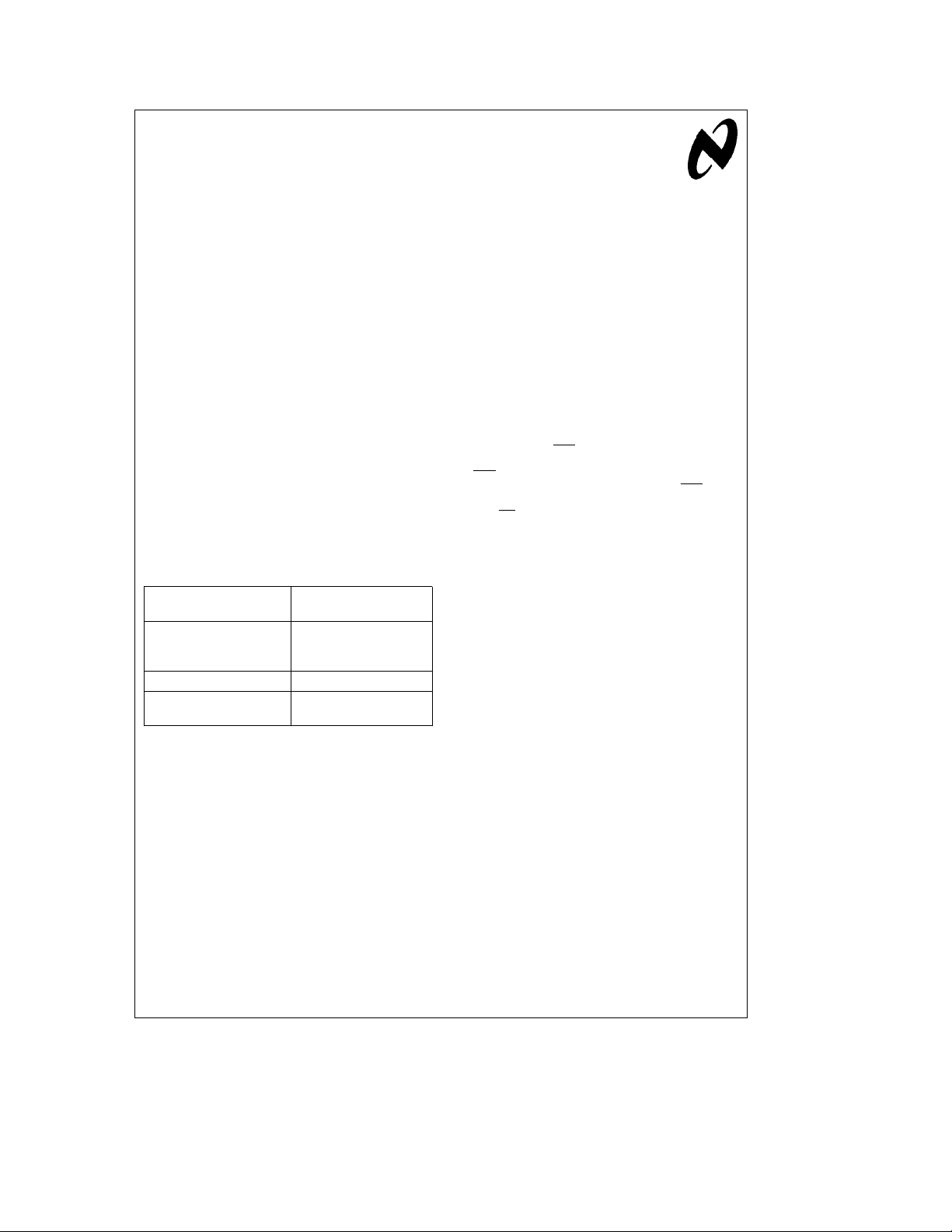
All Control On-Chip
Figure 1
is a block diagram of the DP8409A. the ADS input
strobes the parallel memory address into the row latches
R0–8, the column latches C0– 8, and bank select B0 and
B1. The nine output drivers may be multiplexed between the
row or column input latches, or the 9-bit on-chip refresh
counter. One of four RAS
cess cycle by setting the bank select inputs B0 or B1. All
four RAS
or automatic control is available on-chip for the CAS
while an on-chip buffer is provided to minimize skew associated with WE
All DRAM address and control outputs on the DP8409A can
directly drive in excess of 500 pF, or the equivalent of 88
DRAMs (4 banks of 22 DRAMs). All output drivers are
closely matched, significantly reducing output skew. Each
output stage has symmetrical high and low logic level drive
capability, insuring matched rise and fall time characteristics.
Flexibility and Upgradability to 256k or 1 Mbit DRAMs
The 9 multiplexed address outputs and 9-bit internal refresh
counter of the DP8409A direct addressing capability for
256k DRAMs. Careful design of memory boards, using 64k
DRAMs with the DP8409A, insures direct upgradability to
256k DRAMs. This can be done by simply allowing for board
address extension by two bits and designing the ninth address trace (Q8) of the DP8409A to connect to pin 1 of the
DRAMs (A8). This is, in general, a non-connected pin in
64ks and the ninth address in 256ks. All that need be done
is to remove the 64ks and replace them with 256ks, thereby
increasing the memory on the same board bya4to1ratio.
The resulting development cost saving can be significant.
Although the new 1 Mbit DRAMs require the larger 18 pin
package, which will require a memory board redesign, upgrading the controller portion of the board may need no
redesign when converting from the DP8409A or DP8419 to
the new DP8429 1 Mbit DRAM controller driver.
Three mode pins (M0, M1 and M2) offer externally selectable modes of operation, a key reason for the DP8409A’s
application flexibility (Table II). The operational modes are
divided between external and automatic memory control.
outputs are active during refresh. Either external
output generation.
outputs is selected during an ac-
output,
C
1995 National Semiconductor Corporation RRD-B30M115/Printed in U. S.A.
TL/F/5012
Page 2
Indicates that there is a 3
kX pull-up resistor on
these outputs when they
are disabled.
FIGURE 1. DP8409A Block Diagram
TL/F/5012– 1
TABLE II. DP8409A Mode Select Options
Mode
(RFSH
M2
M1 M0 Mode of Operation Conditions
)
0 0 0 0 Externally Controlled Refresh RF I/OeEOC
1 0 0 1 Auto RefreshÐForced RF I/OeRefresh Request (RFRQ)
2 0 1 0 Internal Auto Burst Refresh RF I/OeEOC
3a 0 1 1 All RAS Auto Write RF I/OeEOC
3b 0 1 1 Externally Controlled All RAS Access All RAS Active
4 1 0 0 Externally Controlled Access
5 1 0 1 Auto Access, Slow t
6 1 1 0 Auto Access, Fast t
, Hidden Refresh
RAH
RAH
7 1 1 1 Set End of Count
Modes 0, 3b, and 4 provide full control of access and refresh for systems with external memory controllers or for
special purpose applications. Here all timing can be directly
controlled by the external system as shown in
Figure 2
.
Modes 1, 5 and 6 provide on-chip automatic access sequencing with hidden refresh capability. A graphic example
of the automatic access modes of the DP8409A is shown in
Figure 3
. All DRAM access timing and control is generated
from one input strobe, RASIN
; no external clock is required.
On-chip delays insure proper address and control sequencing once the valid parallel address is presented to the fallthrough input latches of the DP8409A. When the RASIN
transitions high-to-low, the decoded RAS output transitions
low, strobing the row address into the DRAM array. An onchip delay automatically generates a guaranteed selectable
(mode 5 or 6) row address hold time. At this point, the
DP8409A switches the address outputs from the row latch
to the column latch. Then another on-chip delay generates
a guaranteed column address set-up time before CAS
that the CAS
output automatically strobes the column address into the DRAM array. Read or write cycles are controlled by the system through independent control of the WE
buffer that is provided on-chip to minimize delay skewing.
The automatic access mode makes the dynamic RAM appear static with respect to access timing. In this mode, only
one signal, RASIN
, is needed after valid parallel addresses
are presented to the DP8409A to initiate proper access sequencing. Access timing (RASIN
to CAS), with full output
loading of 88 DRAMs in the auto access mode, is determined by the dash number given on the DP8409A data
sheet. All performance characteristics are specified over the
full operating temperature and supply ranges.
2
,so
Page 3
Drams may be 16k, 64k or 256k
For 4 banks, can drive 16 data
a
bits
6 check bits for ECC.
For 2 banks, can drive 32 data
a
bits
7 check bits for ECC.
For 1 bank, can drive 64 data
a
bits
8 check bits for ECC.
*These outputs may need damping
resistors to prevent overshoot,
undershoot at memories.
FIGURE 2. Typical Application of DP8409A Using External Control and Refresh in Modes 0 and 4
TL/F/5012– 2
FIGURE 3. This figure demonstrates the automatic accessing capability of the DP8409A. Only one strobing edge,
TL/F/5012– 3
RASIN
, is required for generation of all DRAM access timing signals. This is accomplished with on-chip
delay generators, eliminating the need for external delay lines. No access timing clock is necessary.
3
Page 4
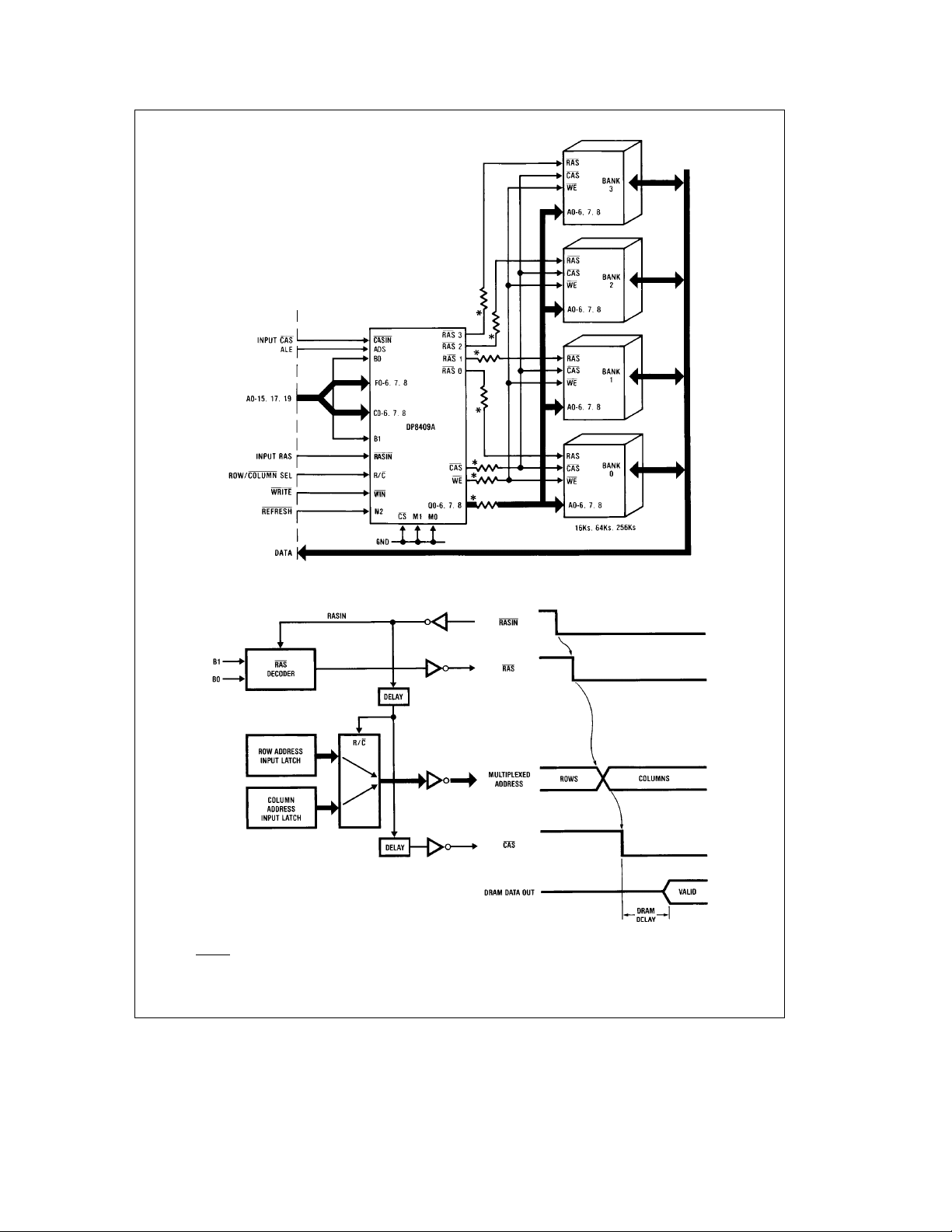
Refreshing
The DP8409A also provdes hidden refresh capability while
in one of the automatic access modes (
Figure 4
). In this
mode, it will automatically perform a refresh without the system being interrupted. To do this, the DP8409A requires two
clock signals, refresh clock (RFCK) which defines the refresh period (usually 16 ms), and RAS
generator clock
(RGCK), which is typically the microprocessor clock.
Highest priority is given to hidden refreshing through use of
level sensing of RFCK. A refresh cycle begins when RFCK
transitions to a high level. If during the time RFCK is high the
DP8409A is deselected (CS
in the high state) and the processor is accessing another portion of the system such as
another memory segment, or ROM, or a peripheral, then a
hidden refresh is performed. When a read or write cycle is
initiated by the processor, the RASIN
transitions low. With CS
high, this causes the present state
input on the DP8409A
of the internal refresh counter to be placed on the address
outputs, followed by the four RAS
outputs transitioning low,
strobing the refresh address into the DRAM array. When the
cycle ends, RASIN
will terminate, thus forcing the RAS outputs back to their inactive state and ending the hidden refresh. The refresh counter is then incremented and another
microprocssor cycle can begin immediately. However, to
save power, the DP8409A will allow only one hidden refresh
to occur during a given RFCK cycle.
In the event that a hidden refresh does not occur, the
DP8409A must force a refresh before the RFCK’s next
positive-going transition.Thesystem is notified afterthenegative-going RFCK transition that a hidden refresh has not oc-
curred, via the refresh request output (RF I/O pin). The system acknowledges the request for a forced refresh by setting M2 (refresh) low on the DP8409A and preventing further access to the DP8409A. The DP8409A then uses
RGCK to generate an automatic forced refresh. The refresh
request pin then returns to the inactive state, and the
DP8409A allows the processor to take full system control
after the forced refresh has been completed.
OCTAL MEMORY DRIVERS
For those applications where the memory array is extremely
large or the controller design is unique to a particular application requirement, specialized high capacitive load address and control buffers are required. However, like any
other element in a DRAM system, selection of the improper
driver can have significant impact on system performance.
In the past, this function has been performed using Schottky
logic family circuits such as the DM74S240 octal inverter or
the DM74S244 octal buffer. The output stages of these devices have good drive capability, but their performance with
heavy capacitive loads is not ideal for DRAM arrays. The
key disadvantage of these devices is their non-symmetrical
rise and fall time characteristics and their long propagation
delays with heavy load capacitance. The former is a result
of impedance mismatch in the upper and lower output
stages. The latter stems from process capability and circuit
design techniques not tailored to the DRAM application.
The combined result of all these factors is increased output
skew in address and control lines when these devices are
used as buffers.
FIGURE 4. Hidden and Forced Refresh Timing of the DP8409A
4
TL/F/5012– 4
Page 5
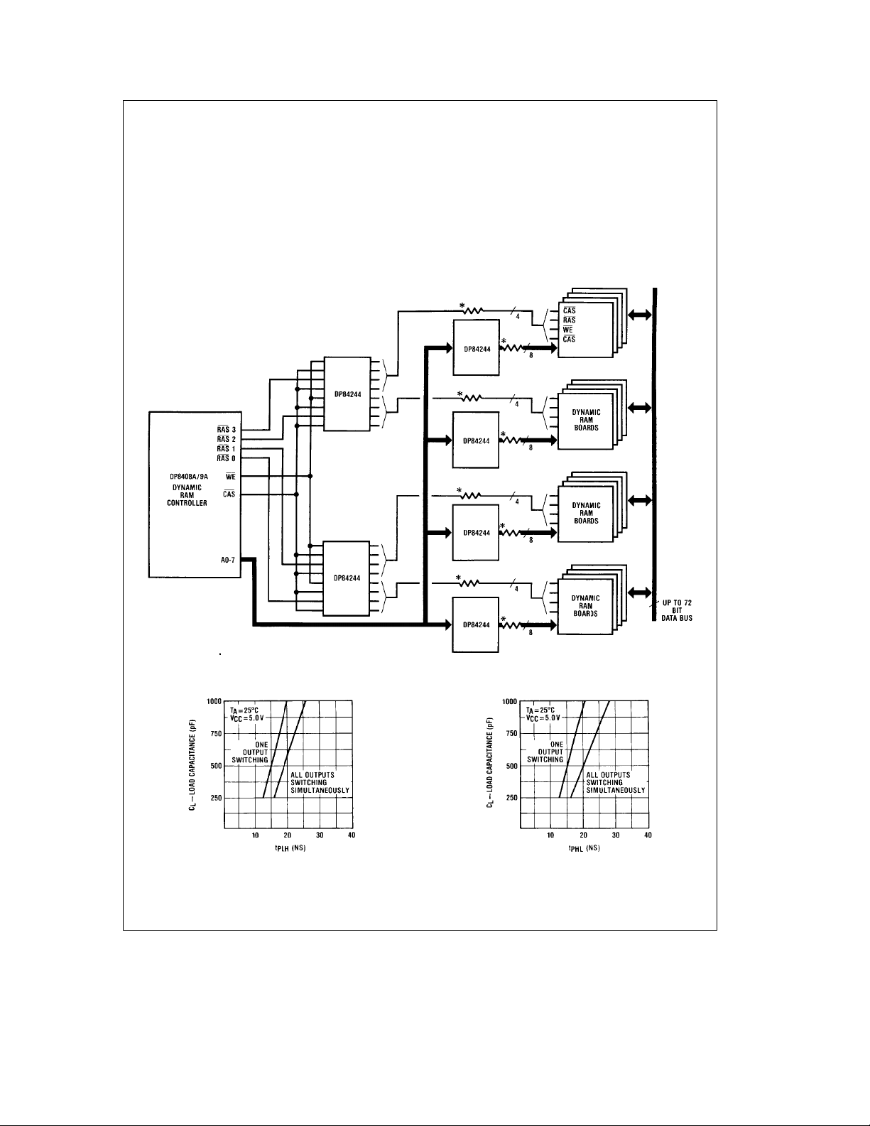
Two new devices are now available for this application. The
DP84240 is pin and function compatible with the
DM74S240. The DP84244 is likewise compatible with the
DM74S244. However, this is where the similarity between
the devices ends. Both the DP84240 and the DP84244
have been designed specifically to drive DRAM arrays.
ure 5
shows a typical application of the DP84244, used in
Fig-
conjunction with the DP8409A, to drive a very large memory
array.
Figures 6a, 6b
show some typical performance curves for
these circuits. Note that, at over 500 pF, the propagation
delay through these drivers is on the order of 15 ns. This
delay includes propagation delay and rise or fall time. Even
*Resistor required depends on DRAM load. See AN-305
‘‘Precautions to Take When Driving Memories.’’
with this high speed, chip power dissipation is still maintained at a reasonable level as demonstrated by the graphs
shown in
Figures 7a, 7b
of power versus frequency.
The DP84240 and the DP84244 are fabricated on a high
performance oxide-isolated Schottky bipolar process. Special circuit techiques have been used to minimize internal
delays and skews. Additionally, both rise and fall time characteristics track closely as a function of load capacitance.
This has been accomplished through impedance matching
of the upper and lower output stages. The result of these
characteristics is a substantial reduction of skew in both the
address and control lines to the DRAM array.
FIGURE 5. The DP84244 Used as a Buffer in a Large Memory Array (greater than 88 DRAMs) Controlled by the DP8409A
TL/F/5012– 5
FIGURE 6a. t
Measured to 2.7V on Output vs. C
PLH
TL/F/5012– 6
L
FIGURE 6b. t
Measured to 0.8V on Output vs. C
PHL
TL/F/5012– 7
L
5
Page 6

FIGURE 7a. Typical Power Dissipation for DP84240 at
e
V
5.5V (All 8 drivers switching simultaneously)
CC
FIGURE 7b. Typical Power Dissipation for DP84244 at
e
V
5.5V (All 8 drivers switching simultaneously)
CC
TL/F/5012– 8
TL/F/5012– 9
The output stages of the DP84240 and the DP84244, although well matched, are relatively low impedance. Output
impedance is under 10X. Some DRAM arrays will require
the addition of damping resistors in series with the outputs
of the drivers. These damping resistors are used to minimize
undershoot which may have a harmful effect on the DRAMs
if allowed to become large. This undershoot is caused by
the high transient currents from the drivers necessary to
drive the capacitive loads. These high currents pass through
a distributed inductive/capacitive circuit created by the
board traces and the DRAM load, causing the undershoot.
The damping resistor has specifically not been placed onchip because its value is dependent on the DRAM array size
and board layout. In fact, address lines will quite often require a different resistor value from the DRAM control lines.
The resistor must be tuned for a particular board layout
since too high a resistor will produce an excessively slow
edge and too low a resistor will not remove the udershoot.
Values for damping resistors may vary from 15X to 150X,
depending on the application. Placing any value of damping
resistor on-chip, other than a value less than the minimum,
severely restricts the application of these high performance
circuits.
Another key advantage of both the DP84240 and the
DP84244 is their low input capacitance. Previous address
buffer/drivers (such as the DM74S240/244) have high input
capacitance. Fast edges at the inputs of these drivers become slower and distorted due to this dynamic input capacitance. This problem must be factored as an additional delay
through these driversÐa delay not shown by the data sheet
specifications. Additionally, the problem becomes increasingly severe as multiple driver inputs are used in parallel for
bus expansion applications.
Both the DP84240 and the DP84244 are designed to significantly reduce both static and dynamic input capacitance.
When these devices are driven with standard logic circuits,
no appreciable overhead delay need be added to the basic
device delay specifications due to input pulse distortion.
ERROR CORRECTION
The determination of whether a DRAM system requires error correction must be resolved early in the system design.
A positive answer to this question may have far-reaching
impact on board development time and component cost. It
is clear, however, that such a decision cannot be taken
lightly.
The type and origin of errors in DRAM systems are many
and can result from a number of sources (Table III). Current
estimates of soft error rates due to alpha particles in 64k
RAMs indicate some hope that these error rates will be similar or possibly better than those found in 16k DRAMsÐbut
the facts are still somewhat unclear. However, it is clear that
the use of 256k DRAMs and the introduction in the near
future of 1 Mbit DRAMs with even smaller memory cells and
greater chip densities will place a significant challenge on
DRAM chip designers to keep these rates down. It is believed by some that error correction may become mandatory in future DRAM system designs. Currently, the decision to
add error correction is not so straightforward. It depends on
many factors, not the least of which is the end user’s perception of its value to system uptime and reliability.
TABLE III. The Sources and Types of Memory Errors
Error
Type
Soft
Hard
Sources System Action
Alpha Particles Temporary system errorÐ
#
System Noise
#
Chip Patterns
#
Power Glitches
#
Stuck Memory Bit Permanent failureÐmay
#
Memory Chip Interface
#
Interface Circuit Failure
#
may be overwritten with a
low probability of repetition
act as logic 1 or 0
Generally, error correction will always be found in highly reliable systems during DRAMs, such as process control equipment, banking terminals, and military systems where high
data integrity and minimum downtime are priorities. However, the importance of error correction has grown substantially, to the point that it is now used as selling feature in the
vast majority of large memory-based systems. In fact, some
major computer houses have adopted quidelines for use by
their designers in the development of DRAM arrays. A
somewhat common set has been foundÐif the memory array is on the order of (/4 million bytes, then word parity
should be used. This permits the detection of single bit errors but does not allow error correction. When the total
memory approaches (/2 million bytes, then double bit error
detection and single bit error correction should be added.
The decision to add error correction to a system is costly,
both in memory overhead and control hardware. Table IV
6
Page 7

TABLE IV. Check Bit Overhead for Multiple Bit Error
Detection and Single Bit Error Correction
Number of Bits Number of Percentage
in Memory Check Bits of Excess
Data Word Required Memory
8 5 63%
16 6 38%
24 6 (7) 25% (29%)
32 7 22%
48 7 (8) 15% (17%)
64 8 13%
Note: The number stated assumes the use of the DP8400; the number in
parentheses is required by other error correction circuits.
lists the number of additional memory chips required to support single bit error correction and double bit error detection
as a function of the memory data word width.
This table also shows the percentage of DRAM overhead
required to implement this function. Adding error correction
also increases the memory access delay, since the information contained in the overhead chips must be analyzed in
each read and generated in each write operation.
DP8400 16-Bit Expandable Error Correction Chip
The DP8400 expandable error checker/corrector is shown
in block diagram form in
Figure 8
. This circuit offers a high
degree of flexibility in applications which range from 8-bit
to 80-bit data words. It is a 16-bit chip that is easily expandable with the simple addition of more DP8400s for each 16bit word increment.
Figures 9a, 9b
write and read memory access cycles.
and9cdemonstrate its basic operation in the
Figure 9a
shows the
normal write cycle, where system data is used by the
DP8400 to generate parity bits, called check bits, based on
certain combinations of the data bits. This combination is
defined by the DP8400’s matrix shown in
Figure 10
. Whenever a ‘‘1’’ occurs in any row, the corresponding input data
bit at the top of the column helps determine the parity for
that check bit labeled at the end of the row. These check
bits are written along with the data at the same memory
address. Also, during a memory write cycle the DP8400
checks system byte parity. This is parity associated with the
data bytes transmitted between the processor and the
memory card. This is an optional feature that may prove
very valuable in multiple board memory systems.
Sometime later a read will occur at this same memory address. The reading of memory data may be performed in
two ways, as shown in
Figures 9b
and9c. In the read cycle,
the DP8400 uses the data read from memory and internally
regenerates check bits using the same matrix. These newly
generated check bits are then compared (using X-OR
gates) with the check bits read from memory to detect errors. The result of this comparison is called a syndrome
word. Any differences in the generated versus read check
bits will result in at least one syndrome bit true. This indicates an error in either the read data or check bit field or
both.
FIGURE 8. DP8400 Simplified Block Diagram
7
TL/F/5012– 10
Page 8

FIGURE 9a. Normal Write Mode with DP8400
TL/F/5012– 11
FIGURE 9b. Normal Read Mode Using the Error Monitoring Method with the DP8400
TL/F/5012– 12
FIGURE 9c. Normal Read Mode Using the Always Correct Method with the DP8400
TL/F/5012– 13
*C2, C3 generate odd parity TL/F/5012– 14
FIGURE 10. DP8400 Matrix
8
Page 9

A key advantage of the DP8400 is that it has three error
flags detailing the type of error occurrence. These are generated using the syndrome word in the manner shown in
Figure 11
. The resulting error type identifications are shown
in Table V. The three error flags allow complete error type
identification, plus the unique determination of double bit
errors, which will be key during the discussion of double bit
error correction. Also, on a memory read, the DP8400 generates byte parity bits for transmission to the processor
along with the data.
TL/F/5012– 15
TABLE V. Error Flags after Normal Read
AE E1 E0 Error Type
0 0 0 No Error
1 1 0 Single Check Bit Error
1 1 1 Single Data Error
1 0 0 Double-Bit Error
All Others Invalid Conditions
There are two basic memory read methods that may be
used with the DP8400. The first is shown in
Figure 9b
and is
called the error monitoring method. Here, the read data is
assumed to be correct and the processor immediately acts
on the data. If the DP8400 detects an error, the processor is
interrupted using the any error flag (AE). Using this method,
there is no detection delay in most memory reads since
errors seldom occur, but when an error does occur, the
processor must be capable of accepting an interrupt and a
read cycle extension to obtain the corrected data from the
DP8400.
A second approach is called the always correct method,
Figure 9c
. In this case, the data is always assumed to be in
error and the processor always waits for the DP8400 to analyze whether an error exits. Then the corrected or unchanged data is read from the DP8400. Although this method results in longer memory read time, every memory read
will always be of the same delay except when a double error
occurs. The selection of which method to use depends on
many factors, including the processor, system structure,
and performance.
Double Bit Error Correct
The probability of double bit errors in DRAM systems is relatively low, but as memory array sizes grow, the occurrence
of these error types must be considered. Adopting certain
practices, such as rewriting a memory location whenever an
error is detected, or using ‘‘memory scrubbing’’ techniques,
can significantly reduce the probability of a double soft error
occurrence. Memory scrubbing is when the system, during
low usage, actually accesses memory solely for the purpose
of identifying and correcting single soft errors. This is an
important technique if there are segments of the memory
that are not always being accessed so that soft error occurrences would not be quickly found.
The occurrence of a double error comprising one soft and
one hard must now be considered. This type of error has a
higher probability than two soft errors. The hard error may
be due to a catastrophic chip failure, and a subsequent soft
error will create two errors. This can be a source of concern
since most error correction chips cannot handle double errors of this type. Therefore, most systems will ‘‘crash’’ when
a catastrophic chip failure is coupled with a soft error in the
same memory address.
The DP8400 has been designed to handle just such an occurrence. It can correct any double bit error, as long as at
least one of the errors is a hard error. The DP8400 does this
without the need for extra hardware required for the basic
double bit detect/single bit correct system implementation.
This method is called the double complement correct technique and is demonstrated in
Figure 12
using a 4-bit data
word for simplicity. In this example, a single hard error is
located in the most significant bit of a particular memory
location and a soft error occurs at the next bit. The position
of the errors is not important since the errors may be distributed in either the data or check bit field or both. First, the
data word and corresponding check bits are written to this
memory location. When a later read of this location occurs,
step A, two errors are directly reported by the DP8400 error
flags. The system detects this, disables memory; and places
the DP8400 in the complement write mode. This causes the
previously read data and check bits to be complemented in
the DP8400 and written back to the same memory address,
step B, writing over the previous soft error. Obviously this
does not modify the cell where the hard error exits. The
system then reads from the same address again, but this
time it places the DP8400 in the complement read mode,
step C. The DP8400 again complements the memory data
and check bits and generates new check bits based on the
new data word. At this point, the chip detects a single bit
error in the bit position where the soft error occurred, and
using the conventional single error correction procedure, returns corrected data to the system, step D.
In the second read, the complement read, the hard error
repeats since this bit location again receives a bit which is
complemented with respect to itself. But the soft error has
been overwritten and does not repeat. Effectively, the memory has complemented the hard bit error position twice and
the soft bit error position only once, while the DP8400 complements both positions twice. Therefore, after the second
read, there is only one error left, the soft error. Since this is
now a single error it can be directly corrected.
9
Page 10

After the complement correct cycle, the memory must be
rewritten with the corrected data since the address now
contains data that is complemented. Full error reporting is
available from the DP8400 after the second read, the complement read, of memory. This is shown in Table VI.
This method is a very effective tool to avoid system crash
due to memory chip failure, and can do much to reduce
unscheduled field service calls. The only time the system
will see a double error that is not directly correctable is
when a double soft error occurs. The probability of this is
very low if the previously discussed techniques are used.
The extra time taken to do an additional read and write of
memory is insignificant when the alternative is a system that
has a catastrophic failure that requires immediate field serv-
ice. Using this technique, software may be provided in the
system to warn the operator that the system is in a degraded operational mode and that field service should occur
shortly. In the meantime, the system will continue to operate
properly. The key to the effectiveness of the DP8400 in this
application is its three error flags which allow complete error
reportingÐincluding a unique double error indication.
DP8402A, 3, 4, 5 32-Bit Error Detector and Corrector
(EDAC)
In addition to the popular DP8400-2 16-bit error checker/
corrector, National offers a family of 32-bit Error Detector
and Correctors (EDACs). With a few exceptions, the
DP8402A, 3, 4, 5 function in a similar manner to the
DP8400-2. One major exception is that the DP8402A, 3, 4, 5
are not expandable beyond 32 bits.
FIGURE 12. Double Error Correct Complement Hard Error
MethodÐ1 Hard Error and 1 Soft Error in Data Bits
TABLE VI. DP8400 Error Flags after a Complement Read
AE E1 E0 Error Type
0 0 0 Two Hard Errors
1 1 0 One Hard Error, One Soft Check Bit Error
1 1 1 One Hard Error, One Soft Data Bit Error
1 0 0 Two Soft Errors, Not Corrected
10
TL/F/5012– 16
Page 11

MICROPROCESSOR INTERFACE CIRCUITS
The major 8-bit, 16-bit and 32-bit microprocessors have different control signal timing. There are also a number of
speed options. The DP8400 family was designed, not for a
specific microprocessor, but rather, significant control flexibility has been provided on both the DP84XX DRAM controller/drivers and the DP84XX error correction devices for
easy interface to any microprocessor. However, a certain
amount of ‘‘glue’’ is necessary to interface to these LSI circuits, usually in the form of a number of MSI/SSI logic circuits. Not only can this be costly in board space utilization,
but it is usually the one place where the most design related
problems occur in system development.
Figures 13
and14show the DP8400 family solution to this
problemÐthe DP84XX2 series of microprocessor interface
circuits.
Figure 13
shows how the DP84300 refresh timer
and the DP84XX2 microprocessor interface circuit connect
to the DP8409A and various microprocessors for a typical
application.
Figure 14
shows the DP8409A and the DP8400
together in a microprocessor-based memory system using
DRAMs, with double bit error detect and single bit error correct capability. In addition, it shows that with the simple addition of some standard data buffers, how the system can
implement byte writing to the DRAM array.
This system structure requires the insertion of few or no wait
states during a memory access cycle, thus maximizing
throughput. The DP84XX2 circuits have been designed to
work with all of National’s DRAM controller/drivers to control refreshing so that system throughput is affected only
when absolutely necessary. First, in any refresh clock period of 16 ms, hidden refreshing is given maximum opportunity. This can be helped with the optional DP84300 refresh
interval generator which offers maximum high-to-low ratioing of RFCK. Second, when a hidden refresh does not occur
in a particular RFCK cycle, a forced refresh may still not
affect a slow access cycle. The worst-case is when an access is pending during a forced refresh, in which case a
three wait state delay is usually the maximum penalty.
Usually two DP84XX2 type chips would be required to interface between any microprocessor and the DP8400/
DP8409A combined system. These chips would handle the
read/write control as well as error detection and correction
control. Table VII shows the individual DP84XX2 circuits
that would be used in systems with no error correction, thus
requiring only the DP84XX DRAM controller/driver function.
²
The select wait input to the
DP843X2 chip inserts a wait
state during accessing. This is
necessary for very fast microprocessors.
FIGURE 13. Connecting the DP8409A between 16-Bit Microprocessor and Memory
TL/F/5012– 17
11
Page 12

The DP8400 DRAM interface family provides complete solutions to memory support. This begins with the LSI functions
such as the DP8400 expandable error checker/corrector
and the DP8409A DRAM controller/driver. It continues with
the DP84240 and the DP84244 high performance buffer/
drivers. Finally, it concludes with easy interface to popular
microprocessors with the use of the DP84XX2 series. It is
the first family of DRAM support circuits designed
for universal applications with multiple microprocessors,
with no manufacturers CPU enjoying a favorite role.
Data sheets and more detailed application information are
available for all the members of the DP8400 family. Contact
your local National Semiconductor representative or National Semiconductor directly.
FIGURE 14. Flexible Application of the DP8409A and DP8400.
This Figure Shows an Application with a 16-Bit Microprocessor.
TABLE VII. The DP84300 Series of Interface
Circuits for Various 16-Bit Microprocessors
Microprocessor
DP84XX DRAM Controller/Driver
System Using
National & TI DP84412
Series 32000
National & TI DP84512
Series 32332
Motorola DP84322 or
68000/08/10 DP84422
Motorola
68020
Intel
80286
Intel
8086/186/88/188
DP84522
DP84532
DP84432
Zilog (2) 74S64
8000 (1) 74S04
TL/F/5012– 18
12
Page 13

13
Page 14

LIFE SUPPORT POLICY
NATIONAL’S PRODUCTS ARE NOT AUTHORIZED FOR USE AS CRITICAL COMPONENTS IN LIFE SUPPORT
DEVICES OR SYSTEMS WITHOUT THE EXPRESS WRITTEN APPROVAL OF THE PRESIDENT OF NATIONAL
SEMICONDUCTOR CORPORATION. As used herein:
1. Life support devices or systems are devices or 2. A critical component is any component of a life
systems which, (a) are intended for surgical implant support device or system whose failure to perform can
into the body, or (b) support or sustain life, and whose be reasonably expected to cause the failure of the life
failure to perform, when properly used in accordance support device or system, or to affect its safety or
with instructions for use provided in the labeling, can effectiveness.
be reasonably expected to result in a significant injury
to the user.
National Semiconductor National Semiconductor National Semiconductor National Semiconductor
Corporation Europe Hong Kong Ltd. Japan Ltd.
1111 West Bardin Road Fax: (
Arlington, TX 76017 Email: cnjwge@tevm2.nsc.com Ocean Centre, 5 Canton Rd. Fax: 81-043-299-2408
Tel: 1(800) 272-9959 Deutsch Tel: (
Fax: 1(800) 737-7018 English Tel: (
AN-302 The DP8400 Family of Memory Interface Circuits
National does not assume anyresponsibility for use of any circuitry described, nocircuit patent licenses are implied and National reserves theright at any time without notice to change saidcircuitry and specifications.
Fran3ais Tel: (
Italiano Tel: (
a
49) 0-180-530 85 86 13th Floor, Straight Block, Tel: 81-043-299-2309
a
49) 0-180-530 85 85 Tsimshatsui, Kowloon
a
49) 0-180-532 78 32 Hong Kong
a
49) 0-180-532 93 58 Tel: (852) 2737-1600
a
49) 0-180-534 16 80 Fax: (852) 2736-9960
 Loading...