

Page 1

DAQPad™-6507/6508
User Manual
Digital I/O Devices for USB
DAQPad-6507/6508 User Manual
December 1998 Edition
Part Number 321724B-01
© Copyright 1997, 1998 National Instruments Corporation. All rights reserved.
Page 2

Internet Support
E-mail: support@natinst.com
FTP Site: ftp.natinst.com
Web Address: http://www.natinst.com
Bulletin Board Support
BBS United States: 512 794 5422
BBS United Kingdom: 01635 551422
BBS France: 01 48 65 15 59
Fax-on-Demand Support
512 418 1111
Telephone Support (USA)
Tel: 512 795 8248
Fax: 512 794 5678
International Offices
Australia 03 9879 5166, Austria 0662 45 79 90 0, Belgium 02 757 00 20, Brazil 011 288 3336,
Canada (Ontario) 905 785 0085, Canada (Québec) 514 694 8521, Denmark 45 76 26 00,
Finland 09 725 725 11, France 01 48 14 24 24, Germany 089 741 31 30, Hong Kong 2645 3186,
Israel 03 6120092, Italy 02 413091, Japan 03 5472 2970, Korea 02 596 7456, Mexico 5 520 2635,
Netherlands 0348 433466, Norway 32 84 84 00, Singapore 2265886, Spain 91 640 0085, Sweden 08 730 49 70,
Switzerland 056 200 51 51, Taiwan 02 377 1200, United Kingdom 01635 523545
National Instruments Corporate Headquarters
6504 Bridge Point Parkway Austin, Texas 78730-5039 USA Tel: 512 794 0100
© Copyright 1997, 1998 National Instruments Corporation. All rights reserved.
Page 3

Important Information
Warranty
The DAQPad-6507 and DAQPad-6508 are warranted against defects in materials and workmanship for a period of
one year from the date of shipment, as evidenced by receipts or other documentation. National Instruments will, at its
option, repair or replace equipment that proves to be defective during the warranty period. This warranty includes parts
and labor.
The media on which you receive National Instruments software are warranted not to fail to execute programming
instructions, due to defects in materials and work man ship, for a peri od of 90 d ays from da te o f sh ipm ent, as evi denced
by receipts or other documentation. National Instruments will, at its option, repair or replace software media that do not
execute programming instructions if National Instruments receives noti ce of su ch defect s d uring th e warranty perio d.
National Instruments does not warrant that the op eration of t he soft ware shall b e uni nterrup ted or erro r free.
A Return Material Authorization (RMA) number must b e ob tain ed fro m th e facto ry an d clearl y mark ed on t he outsi de
of the package before any equipment will be a ccepted for warranty work. National Instruments will pay the shipping c osts
of returning to the owner parts which are covered by warran ty.
National Instruments believes that the information in this manual is accurate. The document has been c arefully reviewed
for technical accuracy. In the event that technical or typographical errors exist, National Instruments reserves the right to
make changes to subsequent editions of th is do cume nt with ou t p rio r no ti ce to hold ers o f thi s ed itio n. The read er sh ou ld
consult National Instruments if errors are suspected. In no event shall National Instruments be liable for any damages
arising out of or related to this docume nt o r th e in form ati on con tai ned in i t.
XCEPT AS SPECIFIED HEREIN
E
ANY WARRANTY OF MERCHANTABILITY OR FITNESS FOR A PARTICULAR PURPOSE
BY FAULT OR NEGLIGENCE ON THE PART OF NATIONAL INSTRUMENTS SHALL BE LIMITED TO THE AMOUNT THERETOFORE PAID BY THE
CUSTOMER
OR INCIDENTAL OR CONSEQUENTIAL DAMAGES, EVEN IF ADVISED OF THE POSSIBILITY THEREOF
National Instruments will apply regardless of the form of action, wh ether in con tract or tort , incl udin g n egli gen ce.
Any action against National Instruments must be brought within one year after the cause of action accrues. National
Instruments shall not be liable for any delay in performance due to causes beyond its reasonable control. The warranty
provided herein does not cover damages, defects, malfuncti ons, or s ervice failur es caused by own er’s fai lure to fol low
the National Instruments installation, operation, or maintenance instructions; owner’s modification of the product;
owner’s abuse, misuse, or negligent acts; and power failure or surges, fire, flood, accident, actions of third parties,
or other events outside reasonable control.
ATIONAL INSTRUMENTS WILL NOT BE LIABLE FOR DAMAGES RESULTING FROM LOSS OF DATA, PROFITS, USE OF PRODUCTS
. N
ATIONAL INSTRUMENTS MAKES NO WARRANTIES, EXPRESS OR IMPLIED, AND SPECIFICALLY DISCLAIMS
, N
USTOMER’S RIGHT TO RECOVER DAMAGES CAUSED
. C
. This limitation of the liability of
,
Copyright
Under the copyright laws, this publication may not be reproduced or transmitted in any form, electronic or mechanical,
including photocopying, recording, storing in an information retrieval system, or translating, in whole or in part, without
the prior written consent of National Instruments Corporation.
Trademarks
ComponentWorks™, CVI™, DAQPad™, LabVIEW™, NI-DAQ™, SCXI™, and VirtualBench™ are trademarks of
National Instruments Corporation.
Product and company names listed are trademarks or trade names of their respective companies.
WARNING REGARDING MEDICAL AND CLINICAL USE OF NATIONAL INSTRUMENTS PRODUCTS
National Instruments products are not designed with com ponent s and tes ting inten ded to ensure a l evel of reliab ilit y
suitable for use in treatment and diagnosis of humans. Applications of National Instruments products invol ving m edical
or clinical treatment can create a potential for accidental injury caused by product failure, or by errors on the part of the
user or application designer. Any use or application of National Instruments products for or involving medical or clinical
treatment must be performed by properly trained and qualified medical personnel, and all traditional medical safeguards,
equipment, and procedures that are appropriate in the particular situation to prevent serious injury or death should always
continue to be used when National Instruments products are being used . National Instrum ents product s are NOT intended
to be a substitute for any form of established process, procedure, or equipment used to monitor or safeguard human health
and safety in medical or clinical treatment.
Page 4

About This Manual
Organization of This Manual...........................................................................................ix
Conventions Used in This Manual................................................................................... x
National Instruments Documentation...................................... .................................. ......xi
Related Documentation........................................... .................................. .......................xii
Customer Communication................................... .................................. ..........................xii
Chapter 1
Introduction
About the DAQPad-6507 and DAQPad-6508 Devices...................................................1-1
What You Need to Get Started........................................................................................1-2
Software Programming Choices......................................................................................1-2
National Instruments Application Software......................................................1-3
NI-DAQ Driver Software..................................................................................1-4
Optional Equipment................................................ .................................. .......................1-5
Custom Cabling.................................................................................................1-6
Unpacking........................................................................................................................1-6
Contents
Chapter 2
Installation and Configuration
Software Installation........................................................................................................2-1
Hardware Installation.......................................................................................................2-1
Configuration...................................................................................................................2-4
Power Considerations ......................................................................................................2-4
Chapter 3
Signal Connections
I/O Connector Pin Description ........................................................................................3-2
I/O Connector Signal Connection Descriptions...............................................................3-3
Port C Pin Assignments.....................................................................................3-4
Cable Assembly Connectors............................................................................................3-4
Digital I/O Signal Connections........................................................................................3-7
Power Connections ..........................................................................................................3-8
Connecting Power Sources to Digital I/O Lines ...............................................3-8
©
National Instruments Corporation v DAQPad-6507/6508 User Manual
Page 5

Contents
Digital I/O State Selection...............................................................................................3-9
High DIO State..................................................................................................3-9
Low DIO State..................................................................................................3-10
Floating DIO State............................................................................................3-11
Timing Specifications......................................................................................................3-12
Mode 1 Input Timing........................................................................................ 3-13
Mode 1 Output Timing .....................................................................................3-14
Mode 2 Bidirectional Timing............................................................................3-15
Chapter 4
Theory of Operation
Interrupt Control Circuitry ..............................................................................................4-2
USB Microcontroller....................................................................................... ................4-2
82C55A Programmable Peripheral Interface ..................................................................4-2
Digital I/O Connector......................................................................................................4-3
Appendix A
Specifications
Appendix B
OKI 82C55A Data Sheet
Appendix C
Common Questions
Appendix D
Customer Communication
Glossary
Index
Figures
Figure 1-1. The Relationship between the Programming Environment,
NI-DAQ, and Your Hardware.................................. ... ............................1-5
Figure 2-1. Connection between Your Computer or USB Hub and
Your DAQPad Device ...........................................................................2-2
DAQPad-6507/6508 User Manual vi
©
National Instruments Corporation
Page 6

Tables
Contents
Figure 2-2. Upstream and Downstream Connections between the
Host Computer and the DAQPad-6507 or DAQPad-6508 ....................2-4
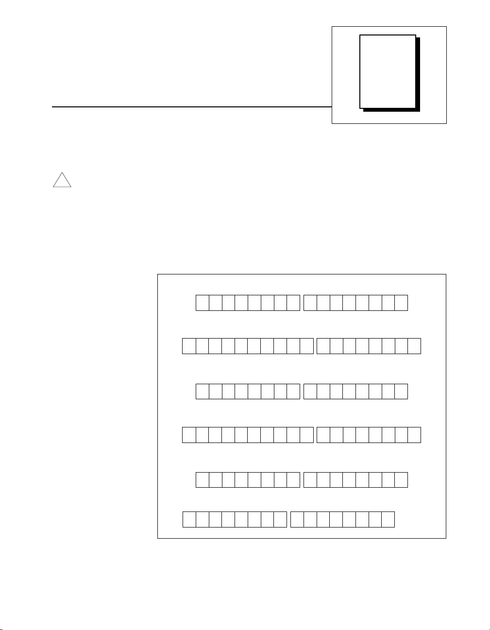
Figure 3-1. Screw Terminal Assignments for the DAQPad-6507.............................3-1
Figure 3-2. Digital I/O Connector Pin Assignments for the DAQPad-6508 .............3-2
Figure 3-3. Cable Assembly Connector Pin Assignments for Pins 1 through 50
of the DAQPad-6508 I/O Connector.......................................................3-5
Figure 3-4. Cable Assembly Connector Pin Assignments for Pins 51 through
100 of the DAQPad-6508 I/O Connector................................................3-6
Figure 3-5. Digital I/O Connections...........................................................................3-7
Figure 3-6. DIO Channel Configured for High DIO State with External Load.........3-9
Figure 3-7. DIO Channel Configured for Low DIO State with External Load .........3-11
Figure 4-1. DAQPad-6507/6508 Devices Block Diagram ........................................4-1
Table 2-1. LED Patterns for DAQPad-6507/6508 States.........................................2-3
Table 3-1. Pin Assignments for the DAQPad-6508 ................................................. 3-3
Table 3-2. Port C Signal Assignments......................................................................3-4
Table 3-3. Timing Signal Descriptions.....................................................................3-12
©
National Instruments Corporation vii DAQPad-6507/6508 User Manual
Page 7

This manual describes the mechanical and electrical aspects of the
DAQPad-6507 and DAQPad-6508 and contains information concerning
their operation and programming.
The DAQPad-6507 and DAQPad-6508 are digital I/O devices for
USB-compatible computers. These devices are designed for
high-performance data acquisition and control for applications in
laboratory testing, production testing, and industrial process monitoring
and control.
Organization of This Manual
The DAQPad-6507/6508 User Manual is organized as follows:
• Chapter 1, Introduction, describes the DAQPad-6507 and
DAQPad-6508; lists what you need to get started; describes software
programming choices, optional equipment, and custom cables; and
explains how to unpack the DAQPad-6507 and DAQPad-6508.
• Chapter 2, Installation and Configuration, describes how to install and
configure the DAQPad-6507 and DAQPad-6508 devices.
• Chapter 3, Signal Connections, includes timing specifications and
signal connection instructions for the DAQPad-6507 and 6508 I/O
connectors.
• Chapter 4, Theory of Operation, contains a functional overvie w of the
DAQPad-6507/6508 devices and explains the operation of each
functional unit making up the DAQPad-6507 or DAQPad-6508.
• Appendix A, Specifications, lists the specifications of the
DAQPad-6507/6508 devices.
• Appendix B, OKI 82C55A Data Sheet, contains the manufacturer data
sheet for the OKI 82C55A (OKI Semiconductor) CMOS
programmable peripheral interface. This interface is used on the
DAQPad-6507/6508 devices.
• Appendix C, Common Questions, contains a list of commonly asked
questions and their answers relating to usage and special features of
your DAQPad-6507/6508 devices.
About
This
Manual
©
National Instruments Corporation ix DAQPad-6507/6508 User Manual
Page 8

About This Manual
• Appendix D, Customer Communication, contains forms you can use to
request help from National Instruments or to comment on our
products.
• The Glossary contains an alphabetical list and description of terms
used in this manual, including abbreviations, acronyms, metric
prefixes, mnemonics, and symbols.
• The Index alphabetically lists the topics in this manual, including the
page where you can find each one.
Conventions Used in This Manual
The following conventions are used in this manual:
This icon to the left of bold italicized text denotes a note, which alerts you
to important information.
!
82C55A 82C55A refers to the OKI 82C55A (OKI Semiconductor) CMOS
< > Angle brackets containing numbers separated by an ellipses represent
bold italic Bold italic text denotes a note, caution, or warning.
italic Italic text denotes emphasis, a cross reference, or an introduction to a key
monospace Text in this font denotes text or characters that you should literally enter
NI-DAQ NI-DAQ refers to the NI-DAQ software for PC compatibles unless
SCXI SCXI stands for Signal Conditioning eXtensions for Instrumentation and is
This icon to the left of bold italicized text denotes a caution, which advises
you of precautions to take to avoid injury, data loss, or a system crash.
programmable peripheral interface.
a range of values associated with a bit or signal name (for example,
ACH<0..7>).
concept.
from the keyboard, sections of code, programming examples, and syntax
examples. This font is also used for the proper names of disk drives, paths,
directories, programs, subprograms, subroutines, device names, functions,
operations, variables, filenames and extensions, and for statements and
comments taken from programs.
otherwise noted.
a National Instruments product line designed to perform front-end signal
conditioning for National Instruments plug-in DAQ devices.
DAQPad-6507/6508 User Manual x
©
National Instruments Corporation
Page 9

National Instruments Documentation
The DAQPad-6507/6508 User Manual is one piece of the documentation
set for your data acquisition (DAQ) system. You could have any of several
types of manuals, depending on the hardware and software in your system.
Use the different types of manuals you have as follows:
• Getting Started with SCXI—If you are using SCXI, this is the first
manual you should read. It gives an overview of the SCXI system and
contains the most commonly needed information for the modules,
chassis, and software.
• Y our SCXI hardware user manuals—If you are using SCXI, read these
manuals next for detailed information about signal connections and
module configuration. They also explain in greater detail how the
module works and contain application hints.
• Your DAQ hardware user manuals—These manuals have detailed
information about the DA Q hardware that plugs into or is connected to
your computer. Use these manuals for hardware installation and
configuration instructions, specification information about your DAQ
hardware, and application hints.
• Software documentation—Examples of software documentation you
may have are the LabVIEW, LabWindows/CVI, and NI-DAQ
documentation sets. After you set up your hardware system, use
either the application software (LabVIEW or LabWindows/CVI)
documentation or the NI-DAQ documentation to help you write your
application. If you have a large and complicated system, it is
worthwhile to look through the software documentation before you
configure your hardware.
• Accessory installation guides or manuals—If you are using accessory
products, read the terminal block and cable assembly installation
guides or accessory device user manuals. They explain how to
physically connect the relevant pieces of the system. Consult these
guides when you are making your connections.
• SCXI Chassis User Manual—If you are using SCXI, read this manual
for maintenance information on the chassis and installation
instructions.
About This Manual
©
National Instruments Corporation xi DAQPad-6507/6508 User Manual
Page 10

About This Manual
Related Documentation
If you are a register-level programmer, the following documents contain
information that you may find helpful as you read this manual:
• Your computer technical reference manual
• USB Specification, Revision 1.1
Customer Communication
National Instruments wants to receive your comments on our products and
manuals. We are interested in the applications you develop with our
products, and we want to help if you have problems with them. To make it
easy for you to contact us, this manual contains comment and configuration
forms for you to complete. These forms are in Appendix D, Customer
Communication, at the end of this manual.
DAQPad-6507/6508 User Manual xii
©
National Instruments Corporation
Page 11

Chapter
Introduction
This chapter describes the DAQPad-6507 and DAQPad-6508; lists what
you need to get started; describes software programming choices, optional
equipment, and custom cables; and explains how to unpack the
DAQPad-6507 and DAQPad-6508.
1
About the DAQPad-6507 and DAQPad-6508 Devices
Thank you for purchasing the National Instruments DAQPad-6507 or
DAQPad-6508. Your DAQPad device is a 96-bit, parallel, digital I/O
interface for computers with USB ports. Four 82C55A programmable
peripheral interface (PPI) chips control the 96 bits of digital I/O. The
82C55A can operate in either a unidirectional or bidirectional mode and
can generate interrupt requests to the host computer. You can program
the 82C55A for almost any 8-bit or 16-bit digital I/O application. All
communication is through a standard, 100-pin, female connector for the
DAQPad-6508 or 100-screw terminals with a strain-relief clamp for the
DAQPad-6507.
Your DAQPad device has a wide input voltage range, and can be powered
from any 9 to 30 VDC power supply.
You can use your DAQPad device in a wide range of digital I/O
applications. With the DAQPad-6507 and DAQPad-6508 devices, you can
interface any PC to any of the following:
• Other computers:
– Another PC with a National Instruments PC-DIO-96/PnP,
PC-DIO-24/PnP, AT-DIO-32F, DAQPad-6507, or DAQPad-6508
– Any other computer with an 8-bit or 16-bit parallel interface
• Centronics-compatible printers and plotters
• Panel meters
• Instruments and test equipment with BCD readouts and/or controls
• Optically isolated, solid-state relays and I/O module mounting racks
©
National Instruments Corporation 1-1 DAQPad-6507/6508 User Manual
Page 12

Chapter 1 Introduction
Note Your DAQPad device cannot sink sufficient current to drive the SSR-OAC-5 and
SSR-OAC-5A output modules. However, it can drive the SSR-ODC-5 output
module and all SSR input modules available from National Instruments.
If you need to drive an SSR-OAC-5 or SSR-OAC-5A, you can either use
a non-inverting digital buffer chip between your DAQPad device and the SSR
backplane, or you can use an MIO series device with appropriate connections
(for example, an SC-205X and cables).
With a DAQPad-6507or DAQPad-6508, your computer can serve as a
digital I/O system controller for laboratory testing, production testing, and
industrial process monitoring and control.
Detailed specifications of the DAQPad-6507 and DAQPad-6508 devices
are in Appendix A, Specifications.
What You Need to Get Started
To set up and use your DAQPad-6507 or DAQPad-6508, you will need the
following:
❑ DAQPad-6507 or DAQPad-6508 device
❑ DAQPad-6507/6508 User Manual
❑ One of the following software packages and documentation:
– NI-DAQ for PC Compatibles
– LabVIEW for Windows
– LabWindows/CVI
– ComponentW orks
– VirtualBench
❑ Your computer
Software Programming Choices
There are several options to choose from when programming your
National Instruments DAQ and SCXI hardware. You can use LabVIEW,
LabWindows/CVI, ComponentWorks, VirtualBench, NI-DAQ, or
register-level programming.
DAQPad-6507/6508 User Manual 1-2
©
National Instruments Corporation
Page 13

National Instruments Application Software
LabVIEW and LabWindows/CVI are innovative program development
software packages for data acquisition and control applications. LabVIEW
uses graphical programming, whereas LabWindows/CVI enhances
traditional programming languages. Both packages include extensive
libraries for data acquisition, instrument control, data analysis, and
graphical data presentation.
LabVIEW features interactive graphics, a state-of-the-art user interface,
and a powerful graphical programming language. The LabVIEW Data
Acquisition VI Library, a series of VIs for using LabVIEW with National
Instruments DAQ hard ware, is included with LabVIEW. The LabVIEW
Data Acquisition VI Library is functionally equivalent to the NI-DAQ
software.
LabWindows/CVI features interactive graphics, a state-of-the-art user
interface, and uses the ANSI standard C programming language. The
LabWindows/CVI Data Acquisition Library , a series of functions for using
LabWindows/CVI with National Instruments DAQ hardware, is included
with the NI-DAQ software kit. The LabWindows/CVI Data Acquisition
Library is functionally equivalent to the NI-DAQ software.
Chapter 1 Introduction
ComponentWorks contains tools for data acquisition and instrument
control built on NI-DAQ driver software. ComponentWorks provides a
higher-level programming interface for building virtual instruments
through standard OLE controls and DLLs. With ComponentWorks, you
can use all of the configuration tools, resource management utilities, and
interactive control utilities included with NI-DAQ.
VirtualBench features virtual instruments that combine DAQ products,
software, and your computer to create a stand-alone instrument with the
added benefit of the processing, display, and storage capabilities of yo ur
computer. VirtualBench instruments load and save waveform data to disk
in the same forms that can be used in popular spreadsheet programs and
word processors.
Using LabVIEW, LabWindows/CVI, ComponentWorks, or VirtualBench
software will greatly reduce the development time for your data acquisition
and control application.
©
National Instruments Corporation 1-3 DAQPad-6507/6508 User Manual
Page 14

Chapter 1 Introduction
NI-DAQ Driver Software
The NI-DAQ driver software is included at no charge with all National
Instruments DAQ hardware. NI-DAQ is not packaged with SCXI or
accessory products, except for the SCXI-1200. NI-DAQ has an extensive
library of functions that you can call from your application programming
environment. These functions include routines for analog input (A/D
conversion), buffered data acquisition (high-speed A/D conversion),
analog output (D/A conversion), waveform generation, digital I/O,
counter/timer operations, SCXI, RTSI, self-calibration, messaging, and
acquiring data to extended memory.
NI-DAQ has both high-level D AQ I/O functions for maximum ease of use
and low-level DAQ I/O functions for maximum flexibility and
performance. Examples of high-level functions are streaming data to disk
or acquiring a certain number of data points. An example of a low-level
function is writing directly to registers on the DAQ device. NI-DAQ does
not sacrifice the performance of National Instruments DAQ devices
because it lets multiple devices operate at their peak performance.
NI-DA Q also internally addresses man y of the comple x issues between the
computer and the DAQ hardware such as programming interrupts and
DMA controllers. NI-DAQ maintains a consistent software interface
among its different versions so that you can change platforms with minimal
modifications to your code. Whether you are using conventional
programming languages or NI-DAQ software, your application uses the
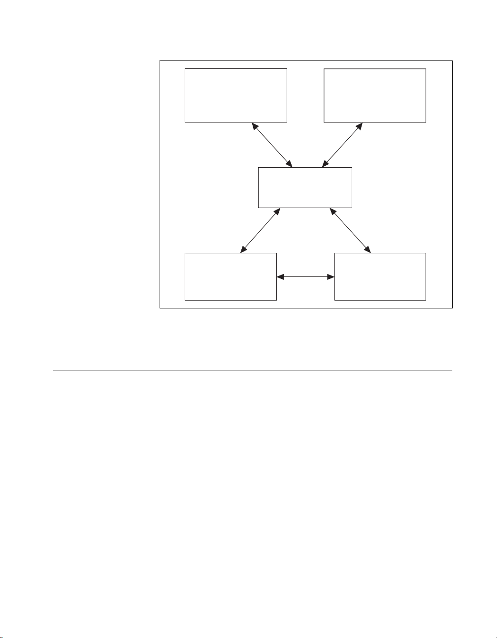
NI-DAQ driver software, as illustrated in Figure 1-1.
DAQPad-6507/6508 User Manual 1-4
©
National Instruments Corporation
Page 15
Chapter 1 Introduction
Figure 1-1. The Relationship between the Programming Environment,
Optional Equipment
Conventional
Programming Environment
DAQ or
SCXI Hardware
NI-DAQ, and Your Hardware
ComponentWorks,
LabVIEW,
LabWindows/CVI, or
VirtualBench
NI-DAQ
Driver Software
Personal
Computer or
Workstation
National Instruments offers a variety of products to use with your
DAQPad-6508 device, including cables, connector blocks, and other
accessories, as follows:
• Cables and cable assemblies
• Connector blocks and unshielded 50-pin screw terminals
• SCXI modules and accessories for isolating, amplifying, exciting, and
multiplexing signals—from up to 3,072 channels—for relays and
analog output
• Low channel count signal conditioning modules, devices, and
accessories, including conditioning for strain gauges and RTDs,
simultaneous sample and hold, and relays
For more specific information about these products, refer to your National
Instruments catalogue or website, or call the office nearest you.
©
National Instruments Corporation 1-5 DAQPad-6507/6508 User Manual
Page 16

Chapter 1 Introduction
Custom Cabling
National Instruments offers cables and accessories for you to prototype
your application or to use if you frequently change device interconnections.
You can connect the DAQPad-6508 device to a wide range of printers,
plotters, test instruments, I/O racks and modules, screw terminal panels,
and almost any device with a parallel interface. The DAQPad-6508 digital
I/O connector is a standard, 100-pin header connector. Adapters for this
header connector expand the interface to four 50-pin ribbon cables, each of
which has the pinout of a PC-DIO-24. The pin assignments of the
expansion cables are compatible with the standard 24-channel I/O module
mounting racks (such as those manufactured by Opto 22 and Gordos).
The CB-100 cable termination accessory is available from National
Instruments for use with your DA QPad device. This accessory includes tw o
50-conductor, flat-ribbon cables and a connector block. You can attach
signal input and output wires to screw terminals on the connector block
and, therefore, connect signals to your DAQPad device I/O connector.
You can use the CB-100 for initial prototyping of an application or in
situations in which your DAQPad device interconnections are frequently
changed. When a final field wiring scheme has been developed, you might
want to develop your own cable.
If you want to develop your own cable, the mating connector for the
DAQPad-6508 is a 100-position, right-angle receptacle without board
locks. Recommended manufacturer part numbers for this mating connector
are as follows:
• AMP Corporation (part number 749076-9)
• Honda Corporation (part number PCS-XE100LFD-HS)
Unpacking
Your DAQPad-6507 or DAQPad-6508 device is shipped in an antistatic
package to prevent electrostatic damage to the device. Electrostatic
discharge can damage several components on the device. To avoid such
damage in handling the device, never touch the exposed pins of connectors.
DAQPad-6507/6508 User Manual 1-6
©
National Instruments Corporation
Page 17

Installation and
Chapter
Configuration
This chapter describes how to install and configure the DAQPad-6507 and
DAQPad-6508 devices.
Software Installation
You should install your software before you install your DAQPad-6507
or DAQPad-6508. If you are using LabVIEW, LabWindows/CVI,
ComponentWorks, or VirtualBench, install this software before installing
NI-DAQ driver software. Refer to your software release notes for your
software for installation instructions.
Note
The DAQPad-6507/6508 devices require NI-DAQ 6.0 or 6.1 for Windows 95, or
NI-DA Q 6.5 or later for Windows 98 (strongly recommended with USB). To ensure
that you have the latest version of NI-DAQ, install it from the CD that ships with
your device.
To install NI-DAQ, refer to your NI-DAQ rel ease not es. Fi nd the
installation section for your operating system and follow the instructions
given there.
2
Hardware Installation
You can connect your DAQPad-6507 or DAQPad-6508 to any available
USB socket. The following are general installation instructions, but consult
your computer user manual or technical reference manual for specific
instructions and warnings. Refer to Figure 2-1 to learn more about making
connections for DAQPad-6507/6508 device.
The following are general installation instructions, but consult your
personal computer user manual or technical reference manual for specific
instructions and warnings.
Note
©
National Instruments Corporation 2-1 DAQPad-6507/6508 User Manual
To ensure proper operation of your DAQP ad device, f ollo w the instructions in the
sequence shown below . Otherwise, your DA QPad might not initialize properly, and
Page 18
Chapter 2 Installation and Configuration
you will need to turn off the DAQPad rocker switch and restart your DAQPad
device again.
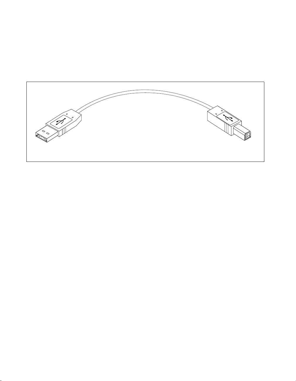
1. Connect the USB cable from the computer port or from any hub to the
port on your DA QPad device. Refer to Figure 2-1 for more information
on connections.
Upstream Connector
Computer or Hub
Downstream Connector
DAQPad
Figure 2-1. Connection between Your Computer or USB Hub and Your DAQPad Device
2. Flip the rocker switch to turn the power on for the DAQPad-6507 or
DAQPad-6508. Your computer should detect your DAQPad device
immediately, and when the computer recognizes your D A QPad device,
the LED on the front panel blinks or lights up, depending on the status
of your device.
3. If the LED comes on after the DAQPad is powered and connected to
the host, it is functioning properly. Refer to Table 2-1 for LED pattern
descriptions for your DAQPad device.
4. Configure your DA QP ad device and any accessories with the NI-D A Q
Configuration Utility.
When the LED blinks, it turns on and off for one second each for as many
times as necessary, then waits three seconds before repeating the cycle.
DAQPad-6507/6508 User Manual 2-2
©
National Instruments Corporation
Page 19
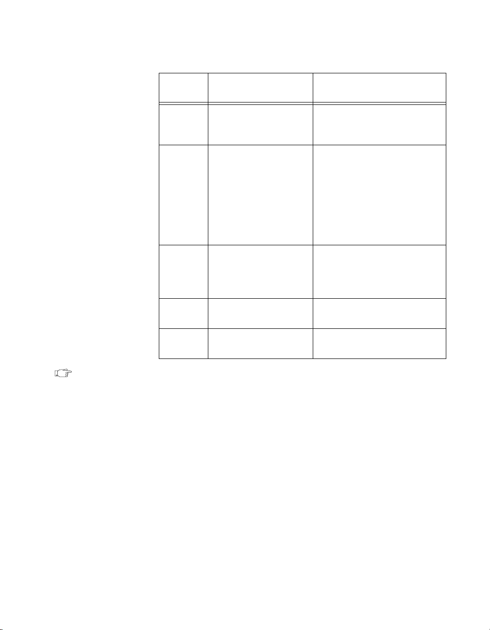
LED
Chapter 2 Installation and Configuration
Table 2-1. LED Patterns for DAQPad-6507/6508 States
DAQPad-6507/6508
State
Description
Off Off or in the low power ,
suspend mode
Your DAQPad device is turned
off or in the low po wer, suspend
mode.
2 blinks Addressed state This pattern is displayed if the
host computer detects your
DAQPad device but cannot
configure it because there are
no system resources available.
If your DA QPad remains in this
state, check your software
installation.
3 blinks Power supply failure This pattern is displayed if you
try to draw too much power
from the USB. You must attach
the external power supply.
4 blinks General error state If this pattern is displayed,
contact National Instruments.
On Configured state Your DAQPad device is
configured.
Note The DAQPad-6507/6508 devices use 100 kΩ resistors for polarity selection.
These signals are controlled by a switch on the back of your DAQPad.
For more information, see the Digital I/O State Selection section in Chapter 3,
Signal Connections.
©
National Instruments Corporation 2-3 DAQPad-6507/6508 User Manual
Page 20
Chapter 2 Installation and Configuration
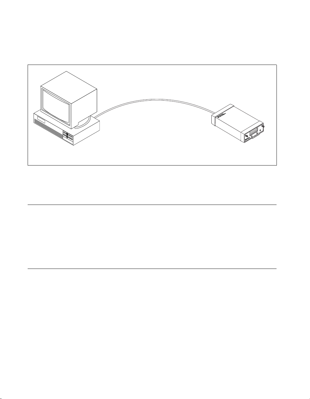
Your DAQPad-6507/6508 device is now installed. Refer to Figure 2-2 to
learn more about upstream and downstream connections between the host
computer and the DAQPad-6507/6508 devices.
Host Computer with
Upstream Connector
Figure 2-2. Upstream and Downstream Connections between the Host Computer
Configuration
The DAQPad-6507/6508 devices are completely software-configurable,
hot Plug and Play instruments. The Plug and Play services query the
instrument and allocate the required resources. The operating system
enables the instrument for operation. Refer to your software documentation
for more information.
Power Considerations
The DAQPad device remains powered up only when the USB cable
connects it to the host computer and the computer is powered up. The host
computer has the ability to go into a power-saving suspend mode. During
this time, your DAQPad device can also go into a low-power mode, and the
I/O signals remain in a fully powered, static state. The advantage of the
low-power mode is that it conserves power. This mode is important if you
are using a battery pack, even though all of the analog circuitry and digital
I/O is powered off and the +5 V supply on the I/O connector is turned off
in this state.
DAQPad-6507/6508 with
Downstream Connector
and the DAQPad-6507 or DAQPad-6508
DAQPad-6507/6508 User Manual 2-4
©
National Instruments Corporation
Page 21

Chapter 2 Installation and Configuration
When the DAQPad exits the suspend mode, NI-DAQ will reinitialize your
DAQPad device and all I/O signals to their default state, regardless of
whether your DAQPad device is in low power mode or static mode. This
action might change the current I/O states and gain if your DA QP ad device
is the low powered, static mode.
The default behavior of your DAQPad device is to go into powered,
static state when the computer enters its suspend mode.
In the powered static state of your DAQPad device, you can draw current
from the +5 V pin on the connector and all digital I/O lines and analog
output channels will be static at a fixed voltage.
Note Refer to the Set_DAQ_Device_Info function in the NI-D AQ Function Reference
Manual to change the settings that determine the behavior of your DA QP ad device
during the suspend state.
If low-power consumption is a concern, the recommended way to turn off
your DAQPad device is with the rocker switch located on the rear panel.
This switch turns your DAQPad device on and off by disconnecting both
the external power supply and the USB supply.
It is also possible to turn off your DAQPad device by detaching the
USB cable while leaving the external supply attached; however, several
milliamperes are continually drawn from the external supply in this case,
although no power is drawn from the USB supply . If you are using a battery
pack, such as the BP-1, it is best to use the rocker switch on the back panel
to prolong the charge of the battery.
©
National Instruments Corporation 2-5 DAQPad-6507/6508 User Manual
Page 22
Chapter
Signal Connections
This chapter includes timing specifications and signal connection
instructions for the DAQPad-6507 and DAQPad-6508 I/O connectors.
Caution
!
Connections that exceed any of the maximum ratings of input or output signals
on the DA QPad-6507/6508 devices can damage the device and the computer. The
description of each signal in this section includes information about maximum
input ratings. National Instruments is
any inaccurate signal connections.
To learn more about screw terminal assignments on the DAQPad-6507,
refer to Figure 3-1.
01234567
APB
012345
G
G
N
N
D
D
01234567
APA
APC
3
liable for any damages resulting from
not
BPA
01234567
BPB
67
01234567
BPC
01234567
CPA
V
cc
01234567
Figure 3-1.
©
National Instruments Corporation 3-1 DAQPad-6507/6508 User Manual
1234567
0V
cc
CPB
01234567
CPC
Screw Terminal Assignments for the DAQPad-6507
01234567
01234567
01234567
DPA
DPB
DPC
Page 23
Chapter 3 Signal Connections
I/O Connector Pin Description
Figure 3-2 shows the pin assignments for the DAQPad-6507/6508 digital
I/O connector.
APC7 CPC7
BPC7 DPC7
APC6 CPC6
BPC6 DPC6
APC5 CPC5
BPC5 DPC5
APC4 CPC4
BPC4 DPC4
APC3 CPC3
BPC3 DPC3
APC2 CPC2
BPC2 DPC2
APC1 CPC1
BPC1 DPC1
APC0 CPC0
BPC0 DPC0
APB7 CPB7
BPB7 DPB7
APB6 CPB6
BPB6 DPB6
APB5 CPB5
BPB5 DPB5
APB4 CPB4
BPB4 DPB4
APB3 CPB3
BPB3 DPB3
APB2 CPB2
BPB2 DPB2
APB1 CPB1
BPB1 DPB1
APB0 CPB0
BPB0 DPB0
APA7 CPA7
BPA7 DPA7
APA6 CPA6
BPA6 DPA6
APA5 CPA5
BPA5 DPA5
APA4 CPA4
BPA4 DPA4
APA3 CPA3
BPA3 DPA3
APA2 CPA2
BPA2 DPA2
APA1 CPA1
BPA1 DPA1
APA0 CPA0
BPA0 DPA0
GND GND
151
252
353
454
555
656
757
858
959
10 60
11 61
12 62
13 63
14 64
15 65
16 66
17 67
18 68
19 69
20 70
21 71
22 72
23 73
24 74
25 75
26 76
27 77
28 78
29 79
30 80
31 81
32 82
33 83
34 84
35 85
36 86
37 87
38 88
39 89
40 90
41 91
42 92
43 93
44 94
45 95
46 96
47 97
48 98
+5 V +5 V
49 99
50 100
Figure 3-2.
Digital I/O Connector Pin Assignments for the DAQPad-6508
DAQPad-6507/6508 User Manual 3-2
©
National Instruments Corporation
Page 24
Chapter 3 Signal Connections
I/O Connector Signal Connection Descriptions
Refer to Table 3-1 for pin assignments for the DAQPad-6508.
Table 3-1.
Pin Assignments for the DAQPad-6508
Pin Signal Name Description
1, 3, 5, 7, 9, 11, 13, 15 APC<7..0> Bidirectional Data Lines for Port C of
PPI A—APC7 is the MSB, APC0 the LSB.
17, 19, 21, 23, 25, 27, 29, 31 APB<7..0> Bidirectional Data Lines for Port B of
PPI A—APB7 is the MSB, APB0 the LSB.
33, 35, 37, 39, 41, 43, 45, 47 APA<7..0> Bidirectional Data Lines for Port A of
PPI A—AP A7 is the MSB, APA0 the LSB.
2, 4, 6, 8, 10, 12, 14, 16 BPC<7..0> Bidirectional Data Lines for Port C of
PPI B—BPC7 is the MSB, BPC0 the LSB.
18, 20, 22, 24, 26, 28, 30, 32 BPB<7..0> Bidirectional Data Lines for Port B of
PPI B—BPB7 is the MSB, BPB0 the LSB.
34, 36, 38, 40, 42, 44, 46, 48 BPA<7..0> Bidirectional Data Lines for Port A of
PPI B—BPA7 is the MSB, BPA0 the LSB.
51, 53, 55, 57, 59, 61, 63, 65 CPC<7..0> Bidirectional Data Lines for Port C of
PPI C—CPC7 is the MSB, CPC0 the LSB.
67, 69, 71, 73, 75, 77, 79, 81 CPB<7..0> Bidirectional Data Lines for Port B of
PPI C—CPB7 is the MSB, CPB0 the LSB.
83, 85, 87, 89, 91, 93, 95, 97 CPA<7..0> Bidirectional Data Lines for Port A of
PPI C—CPA7 is the MSB, CPA0 the LSB.
52, 54, 56, 58, 60, 62, 64, 66 DPC<7..0> Bidirectional Data Lines for Port C of
PPI D—DPC7 is the MSB, DPC0 the LSB.
68, 70, 72, 74, 76, 78, 80, 82 DPB<7..0> Bidirectional Data Lines for Port B of
PPI D—DPB7 is the MSB, DPB0 the LSB.
84, 86, 88, 90, 92, 94, 96, 98 DPA<7..0> Bidirectional Data Lines for Port A of
PPI D—DP A7 is the MSB, DPA0 the LSB.
49, 99 +5 V +5 V—These pins are connected to the
DAQPad’s +5 VDC supply.
50, 100 GND Ground—These pins are connected to the
computer’s ground signal.
Note
: Pins 49 and 99 are connected to the +5 V PC power supply via a 1 A self-resetting fuse.
©
National Instruments Corporation 3-3 DAQPad-6507/6508 User Manual
Page 25
Chapter 3 Signal Connections
Port C Pin Assignments
The signals assigned to port C depend on the mode in which the 82C55A is
programmed in your application software. In mode 0, port C is considered
as two 4-bit I/O ports. In modes 1 and 2, port C is used for status
and handshaking signals with zero, two, or three lines available for
general-purpose input/output. Table 3-2 summarizes the signal
assignments of port C for each programmable mode.
Caution
!
Programming
Mode
During programming, be aware that each time a port is configured, output ports A
and C are reset to 0, and output port B is undefined.
Table 3-2.
Port C Signal Assignments
Group A Group B
PC7 PC6 PC5 PC4 PC3 PC2 PC1 PC0
Mode 0 I/O I/O I/O I/O I/O I/O I/O I/O
Mode 1 Input I/O I/O IBF
STBA* INTRASTBB* IBFBBINTR
A
Mode 1 Output OBFA* ACKA* I/O I/O INTRAACKB* OBFB* INTR
Mode 2 OBFA* ACKA* IBF
STBA* INTRAI/O I/O I/O
A
* Indicates that the signal is active low; refer to Table 3-3 for signal name definitions.
Cable Assembly Connectors
The cable assembly referred to in the Optional Equipment section in
Chapter 1, Introduction, is an assembly of two 50-pin cables and three
connectors. Both cables are joined to a single connector on one end and to
individual connectors on the free ends. The 100-pin connector that joins the
two cables plugs into the I/O connector of the DAQPad-6508. The other
two connectors are 50-pin connectors, one of which is connected to pins 1
through 50, and the other is connected to pins 51 through 100 of the
DAQPad-6508 I/O connector. The cables are labelled Position 1-50 and
51-100, respectively. Figures 3-3 and 3-4 show the pin assignments for the
50-pin connectors on the cable assembly.
B
B
DAQPad-6507/6508 User Manual 3-4
©
National Instruments Corporation
Page 26

Chapter 3 Signal Connections
APC7
APC6
APC5
APC4
APC3
APC2
APC1
APC0
APB7
APB6
APB5
APB4
APB3
APB2
APB1
APB0
APA7
APA6
APA5
APA4
APA3
APA2
APA1
APA0
+5 V
12
34
56
78
910
11 12
13 14
15 16
17 18
19 20
21 22
23 24
25 26
27 28
29 30
31 32
33 34
35 36
37 38
39 40
41 42
43 44
45 46
47 48
49 50
BPC7
BPC6
BPC5
BPC4
BPC3
BPC2
BPC1
BPC0
BPB7
BPB6
BPB5
BPB4
BPB3
BPB2
BPB1
BPB0
BPA7
BPA6
BPA5
BPA4
BPA3
BPA2
BPA1
BPA0
GND
Figure 3-3. Cable Assembly Connector Pin Assignments for Pins 1 through 50
of the DAQPad-6508 I/O Connector
©
National Instruments Corporation 3-5 DAQPad-6507/6508 User Manual
Page 27
Chapter 3 Signal Connections
CPC7
CPC6
CPC5
CPC4
CPC3
CPC2
CPC1
CPC0
CPB7
CPB6
CPB5
CPB4
CPB3
CPB2
CPB1
CPB0
CPA7
CPA6
CPA5
CPA4
CPA3
CPA2
CPA1
CPA0
+5 V
12
34
56
78
910
11 12
13 14
15 16
17 18
19 20
21 22
23 24
25 26
27 28
29 30
31 32
33 34
35 36
37 38
39 40
41 42
43 44
45 46
47 48
49 50
DPC7
DPC6
DPC5
DPC4
DPC3
DPC2
DPC1
DPC0
DPB7
DPB6
DPB5
DPB4
DPB3
DPB2
DPB1
DPB0
DPA7
DPA6
DPA5
DPA4
DPA3
DPA2
DPA1
DPA0
GND
Figure 3-4. Cable Assembly Connector Pin Assignments for Pins 51 through 100
of the DAQPad-6508 I/O Connector
DAQPad-6507/6508 User Manual 3-6
©
National Instruments Corporation
Page 28
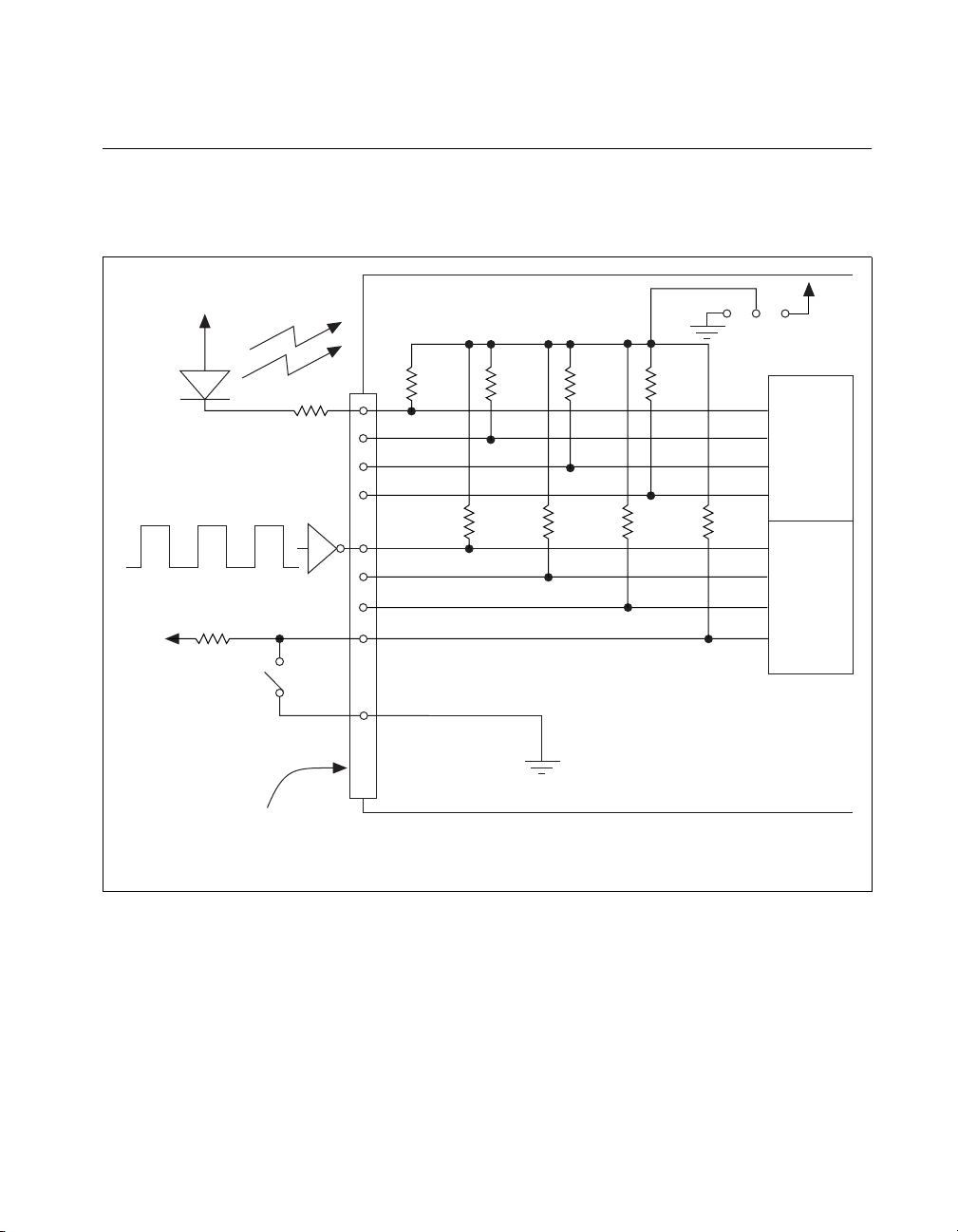
Digital I/O Signal Connections
Pins 1 through 48 and pins 51 through 98 of the I/O connector are digital
I/O signal pins. Figure 3-5 depicts signal connections for three typical
digital I/O applications.
Chapter 3 Signal Connections
+5 V
LED
+5 V
TTL Signal
Switch *
I/O Connector
41
43
45
47
67
69
71
73
+5 V
Front Switch
100 kΩ100 kΩ 100 kΩ 100 kΩ
PPI A
Port A
APA<3..0>
100 kΩ 100 kΩ 100 kΩ 100 kΩ
PPI C
Port B
CPB<7..4>
50, 100
GND
DAQPad-6507/6508
* Complex switch circuitry is not shown in order to simplify the figure.
Figure 3-5.
Digital I/O Connections
In Figure 3-5, PPI A, port A is configured for digital output, and PPI C,
port B is configured for digital input. Digital input applications include
receiving TTL signals and sensing external device states, such as the state
of the switch in Figure 3-5. Digital output applications include sending
TTL signals and driving external devices such as the LED shown in
Figure 3-5.
©
National Instruments Corporation 3-7 DAQPad-6507/6508 User Manual
Page 29

Chapter 3 Signal Connections
Power Connections
Two pins on the I/0 connector supply +5 V from your DAQPad
device’s power supply through a self-resetting fuse. The fuse resets
automatically within a few seconds after the overcurrent condition is
removed. These two pins are referenced to DGND and can be used to
power external digital circuitry.The power rating is indicated below.
Power rating: +4.65 VDC to +5.25 VDC at 1 A combined total for both pins
Caution
!
Never connect the +5 V power pins (pins 49 and 99) directly to analog or digital
ground or to any other voltage source on your DAQP ad device or any other device.
Doing so can damage your DAQ Pad device and the computer. National
Instruments is not liable for damages resulting from such a connection.
Pins 49 and 99 of the I/O connector are connected to the +5 V supply of the
DAQPad-6507/6508 devices. You can power the DAQPad-6507 or
DA QPad-6508 from either USB power or an e xternal source. The D A QPad
uses USB power when the external source is not plugged in. USB power
limits any device from using more than 0.5 A. If you are running from USB
power (that is, if your external power source is not plugged in), you have
only 150 mA to drive signals and supply power for your circuitry. If you
require more power than 150 mA, attach the external power source. Also,
your host computer might turn off power to your DAQPad device if no
activity is detected. This cuts the power to any external circuitry powered
by your DAQPad device if you are not using an external power source.
Refer to Power Considerations, in Chapter 2, Installation and
Configuration, of this manual.
Connecting Power Sources to Digital I/O Lines
Caution
!
Always turn your DAQPad on before applying external power to the digital I/O
(DIO) lines. If your DA QP ad is off and external power is applied to the DIO lines,
your DAQPad may be damaged. National Instruments is not liable for damage
caused by incorrect power sequencing.
When supplying power to DIO lines, we strongly recommend you use the
+5 V source from the DAQPad. If you must use an external power source,
it is important to sequence the power correctly—DAQ Pad first, then
external power—to prevent damage to the CMOS circuits. Because of a
trait common to all CMOS circuits, applying external power first may cause
current to flow incorrectly, damaging the circuit.
DAQPad-6507/6508 User Manual 3-8
©
National Instruments Corporation
Page 30

Digital I/O State Selection
You can power up the digital I/O lines for the DAQPad-6507/6508 devices
in a user-defined state. The DAQPad-6507/6508 devices facilitate
user-configurable pull-up or pull -down tasks. Each DIO channel is
connected to a 100 kΩ resistor and can be pulled high or low using the front
panel switch. You can use this switch to pull all 96 DIO lines high or low,
or you can allow the lines to float. However, if all lines are high, you might
want to pull some lines low. To do this properly, you must understand the
nature of the drive current on those lines and adhere to TTL logic levels, or
you can let the lines float and tie them all high or low as necessary.
High DIO State
If you select the pulled-high mode, each DIO line will be pulled to VCC
(+5 VDC) with a 100 kΩ resistor. To pull a specific line low, connect
between that line and ground and use a pull-down resistor (R
will give you a maximum of 0.4 VDC. The DIO lines provide a maximum
of 2.5 mA at 3.7 V in the high state. Use the largest possible resistor so that
you do not use more current than necessary to perform the pull-down task.
Also, make sure the resistor value is not so large that leakage current from
the DIO line along with the current from the 100 kΩ pull-up resistor drives
the voltage at the resistor above a TTL low level of 0.4 VDC.
Chapter 3 Signal Connections
) whose value
L
DAQPad-6507/6508
82C55A
Figure 3-6.
©
National Instruments Corporation 3-9 DAQPad-6507/6508 User Manual
DIO Channel Configured for High DIO State with External Load
100 kΩ
+5 V
GND
Digital I/O Line
R
L
Page 31

Chapter 3 Signal Connections
Example:
At power up, the device is configured for input and, by default, all DIO
lines are high. To pull one channel low, follow these steps:
1. Install a load (R
). Remember that the smaller the resistance, the
L
greater the current consumption and the lower the voltage (V).
2. Using the following formula, calculate the largest possible load to
maintain a logic low level of 0.4 V and supply the maximum driving
current (I).
V = I * R
⇒ RL = V / I, where:
L
V= 0.4 V is the voltage across R
L
I = 46 µA + 10 µA is the 4.6 V across the 100 kΩ pull-up
resistor and 10 µA from 82C55 leakage current
Therefore:
R
= 7.1 kΩ is the 0.4 V / 56 µA
L
This resistor value, 7.1 kΩ, provides a maximum of 0.4 V on the DIO line
at power up. You can substitute smaller resistor values, but they will draw
more current, leaving less drive current for other circuitry connected to this
line. The 7.1 kΩ resistor reduces the amount of a logic high source current
by 0.4 mA with a 2.8 V output.
Low DIO State
If you select pulled-low mode, each DIO line will be pulled to GND
(0 VDC) using a 100 kΩ resistor. If you want to pull a specific line high,
connect a pull-up resistor that gives you a minimum of 2.8 VDC. The DIO
lines are capable of sinking a maximum of 2.5 mA at 0.4 V in the low state.
Use the largest possible resistance value so that you do not use more current
than necessary to perform the pull-up task.
Also, make sure the pull-up resistor value is not so large that leakage
current from the DIO line along with the current from the 100 kΩ
pull-down resistor brings the voltage at the resistor below a TTL-high le vel
of 2.8 VDC.
DAQPad-6507/6508 User Manual 3-10
©
National Instruments Corporation
Page 32

Chapter 3 Signal Connections
DAQPad-6507/6508
82C55A
100 kΩ
GND
Figure 3-7. DIO Channel Configured for Low DIO State with External Load
+5 V
R
L
Digital I/O Line
Example:
The switch is set in the low DIO state, which means all DIO lines are pulled
low. If you want to pull one channel high, follow these steps:
1. Install a load (R
). Remember that the smaller the resistance, the
L
greater the current consumption and the lower the voltage (V).
2. Using the following formula, calculate the largest possible load to
maintain a logic high level of 2.8 V and supply the maximum sink
current (I).
V = I * R
⇒ RL = V / I, where:
L
V = 2.2 V is the voltage across R
L
I = 28 µA + 10 µA is the 2.8 V across the 100 kΩ pull-up
resistor and 10 µA from 82C55A leakage current
Therefore:
R
= 5.7 kΩ is the 2.2 V / 38 µA
L
This resistor value, 5.7 kΩ, provides a minimum of 2.8 V on the DIO line
at power up. You can substitute smaller resistor values but they draw more
current, leaving less sink current for other circuitry connected to this line.
The 5.7 kΩ resistor reduces the amount of a logic low sink current by
0.8 mA with a 0.4 V output.
Floating DIO State
The DIO lines are not pulled high or low by your DAQPad device in this
configuration. Use an external 100 kΩ resistor to pull the line to the state
you want.
©
National Instruments Corporation 3-11 DAQPad-6507/6508 User Manual
Page 33

Chapter 3 Signal Connections
Timing Specifications
This section lists the timing specifications for handshaking with the
DAQPad-6507/6508 devices. The handshaking lines STB* and IBF
synchronize input transfers. The handshaking lines OBF* and ACK*
synchronize output transfers.
The signals in Table 3-3 are used in the timing diagrams later in this
chapter.
Table 3-3.
Timing Signal Descriptions
Name Type Description
STB* Input Strobe Input—A low signal on this handshaking line loads data
into the input latch.
IBF Output Input Buffer Full—A high signal on this handshaking line indicates
that data has been loaded into the input latch. This is an input
acknowledge signal.
ACK* Input Acknowledge Input—A low signal on this handshaking line
indicates that the data written to the port has been accepted. This
signal is a response from the external device indicating that it has
received the data from the DAQPad-6507/6508 devices.
OBF* Output Output Buffer Full—A low signal on this handshaking line
indicates that data has been written to the port.
INTR Output Interrupt Request—This signal becomes high when the 82C55A
requests service during a data transfer. The appropriate interrupt
enable bits must be set to generate this signal.
RD* Internal Read Signal—This signal is the read signal generated from the
control lines of the computer I/O expansion bus.
WR* Internal Write Signal—This signal is the write signal generated from the
control lines of the computer I/O expansion bus.
DA T A Bidirectional Data Lines at the Specified Port—This signal indicates the
availability of data on the data lines at a port that is in the output
mode. If the port is in the input mode, this signal indicates when the
data on the data lines should be valid.
DAQPad-6507/6508 User Manual 3-12
©
National Instruments Corporation
Page 34

Mode 1 Input Timing
The following figure illustrates the timing specifications for an input
transfer in mode 1.
STB *
Chapter 3 Signal Connections
T1
T2
T4
T7
IBF
T6
INTR
RD *
T3
T5
DATA
Name Description Minimum Maximum
T1 STB* pulse width 100 —
T2 STB* = 0 to IBF = 1 — 150
T3 Data before STB* = 1 20 —
T4 STB* = 1 to INTR = 1 — 150
T5 Data after STB* = 1 50 —
T6 RD* = 0 to INTR = 0 — 200
T7 RD* = 1 to IBF = 0 — 150
All timing values are in nanoseconds.
©
National Instruments Corporation 3-13 DAQPad-6507/6508 User Manual
Page 35

Chapter 3 Signal Connections
Mode 1 Output Timing
The following figure illustrates the timing specifications for an output
transfer in mode 1.
WR*
OBF*
INTR
ACK*
DATA
T3
T4
T1
T5
T2
T6
Name Description Minimum Maximum
T1 WR* = 0 to INTR = 0 — 250
T2 WR* = 1 to output — 200
T3 WR* = 1 to OBF* = 0 — 150
T4 ACK* = 0 to OBF* = 1 — 150
T5 ACK* pulse width 100 —
T6 ACK* = 1 to INTR = 1 — 150
All timing values are in nanoseconds.
DAQPad-6507/6508 User Manual 3-14
©
National Instruments Corporation
Page 36

Mode 2 Bidirectional Timing
The following figure illustrates the timing specifications for bidirectional
transfers in mode 2.
T1
Chapter 3 Signal Connections
WR *
T6
OBF *
INTR
T7
ACK *
T3
STB *
T4
T10
IBF
RD *
T2
T5
T8
T9
DATA
Name Description Minimum Maximum
T1 WR* = 1 to OBF* = 0 — 150
T2 Data before STB* = 1 20 —
T3 STB* pulse width 100 —
T4 STB* = 0 to IBF = 1 — 150
T5 Data after STB* = 1 50 —
T6 ACK* = 0 to OBF = 1 — 150
T7 ACK* pulse width 100 —
T8 ACK* = 0 to output — 150
T9 ACK* = 1 to output float 20 250
T10 RD* = 1 to IBF = 0 — 150
All timing values are in nanoseconds.
©
National Instruments Corporation 3-15 DAQPad-6507/6508 User Manual
Page 37

Chapter
Theory of Operation
This chapter contains a functional overview of the DAQPad-6507/6508
devices and explains the operation of each functional unit making up the
DAQPad-6507 or DAQPad-6508.
The block diagram in Figure 4-1 illustrates the key functional components
of the DAQPad-6507/6508 devices.
Configuration Port
Data
2
USB Interface
Power Supply
Controls
Power Supply
Controls
Serial
Configuration
EEPROM
3
Serial EEPROM
USB Microcontroller
Intel 8x930AX
Serial Port
Interface
External Power
5 V Supply
Power Supply
Switch
Interrupt
Request
Bus
Interface
Firmware
EEPROM
Power Supply
Controls
Wait State
Controls
Address/Data
FPGA
SRAM
Interrupt
Controls
Address/Data
Bus
Address/Data
Control Lines
Address/Data
Control Lines
Control Lines
Address/Data
Control Lines
Address/Data
Address/Data
4
+5 V
500 mA
82C55
PPI (A)
6
82C55
PPI (B)
6
6
82C55
PPI (C)
6
82C55
PPI (D)
82C53
Timer
Port A
Port B
Port C
Port A
Port B
Port C
Port A
Port B
Port C
Port A
Port B
Port C
8
8
8
8
8
8
8
8
8
Terminal Blocks (100 POS)
8
8
8
Figure 4-1.
©
National Instruments Corporation 4-1 DAQPad-6507/6508 User Manual
DAQPad-6507/6508 Devices Block Diagram
Page 38

Chapter 4 Theory of Operation
Interrupt Control Circuitry
Interrupt control circuitry enables and disables interrupts. Two
software-controlled registers determine which devices, if any, generate
interrupts in the interrupt circuitry of the DAQPad-6507/6508 devices.
Each of the four 82C55A devices has two interrupt lines, PC3 and PC0,
connected to the interrupt circuitry.
Each of the eight interrupt lines can interrupt the host computer if the
interrupt circuitry is enabled and the corresponding enable bit is set.
Normally, PC3 and/or PC0 of the 82C55A devices are controlled by the
handshaking circuitry; however, you can configure and use either of these
two lines for input and external interrupts. An interrupt occurs on the
low-to-high transition of the signal line. Refer to Appendix B, OKI 82C55A
Data Sheet for more information.
USB Microcontroller
The USB controller is a special microcontroller that has circuitry necessary
to transmit and receive data over USB itself. It maintains information about
the status of the bus and follows the USB protocol to acquire and send
information over the bus. The microcontroller receives instruction codes
over USB, parses the instructions, and executes them. NI-DAQ handles all
interaction with the microcontroller.
82C55A Programmable Peripheral Interface
The four 82C55A PPI chips are the heart of the DAQPad-6507/6508
devices. Each of these chips has 24 programmable I/O pins that represent
three 8-bit ports: PA, PB, and PC. Each port can be programmed as an input
or an output port. The 82C55A has three modes of operation: simple I/O
(mode 0), strobed I/O (mode 1), and bidirectional I/O (mode 2). In modes
1 and 2, the three ports are divided into two groups: group A and group B.
Each group has eight data bits and four control and status bits from port C
(PC). Modes 1 and 2 use handshaking signals from port C to synchronize
data transfers. Refer to Appendix B, OKI 82C55A Data Sheet, for more
detailed information.
DAQPad-6507/6508 User Manual 4-2
©
National Instruments Corporation
Page 39

Digital I/O Connector
All digital I/O is transmitted through a standard, 100-pin, female connector
for the DAQPad-6508 or 100-pin screw terminal with a strain-relief clamp
for the DAQPad-6507. Pins 49 and 99 are connected to +5 V through a
self-restarting protection fuse (F1). See Figure 4-1 for its location. This
+5 V supply is often required to operate I/O module mounting racks.
Pins 50 and 100 are connected to ground. See the Optional Equipment
section in Chapter 1, Introduction, as well as Chapter 2, Installation and
Configuration, and the Digital I/O Signal Connections section in
Chapter 3, Signal Connections, for additional in formation.
Chapter 4 Theory of Operation
©
National Instruments Corporation 4-3 DAQPad-6507/6508 User Manual
Page 40

Appendix
Specifications
This appendix lists the specifications of the DAQPad-6507/6508 devices.
These specifications are typical at 25° C, unless otherwise stated. The
operating temperature range is 0° to 70° C.
Digital I/O
Number of channels...............................96 I/O
Compatibility .........................................TTL
Absolute max voltage rating..................–0.5 to +5.5 V with respect
Handshaking...........................................Requires 1 port
Power-on state........................................Configured as inputs, high
Data transfers .........................................Interrupts, programmed I/O
A
to GND
(selectable on the front panel
switch)
Digital logic levels
Level Min Max
Input low voltage
Input high voltage
Input low current (V
Input high current (V
Output low voltage (I
Output high voltage (I
Input current (0 < Vin < 5 V) –1.0 µA 1.0 µA
©
National Instruments Corporation A-1 DAQPad-6507/6508 User Manual
= 0.8 V)
in
= 2.4 V)
in
= 2.5 mA)
out
= -2.5 mA)
out
–0.3 V
2.2 V
—
—
0 V
3.7 V
0.8 V
5.3 V
–1.0 µA
1.0 µA
0.4 V
5.0 V
Page 41

Appendix A Specifications
Output signals
Pin 49 and pin 99 (at +5 V).............0.5 A max
Note The total combined current output from pins 49 and 99 may be limited by the
available current from the USB. If you do not have the external power supply
connected, you have only 150 mA of current available to drive all outputs,
including DIO lines.
Transfer rates..........................................Up to 60 S/s
Power Requirement
External
9 to 30 VDC.....................................12 W max
USB
4.40 to 5.25 VDC.............................220 mA typ, 500 mA max
Physical
Dimensions.............................................22.9 by 14.6 cm (9.0 by 5.7 in.)
I/O connector
DAQPad-6507................................ .100-screw terminals
DAQPad-6508.................................100-pin female, 0.050 series
D-type
Environment
Operating temperature............................0° to 70° C
Storage temperature................................–55° to 150° C
Relative humidity ...................................5% to 90% noncondensing
DAQPad-6507/6508 User Manual A-2
©
National Instruments Corporation
Page 42

Appendix
OKI 82C55A Data Sheet
This appendix contains the manufacturer data sheet for the
OKI 82C55A
interface. This interface is used on the DAQPad-6507/6508 devices.
1
(OKI Semiconductor) CMOS programmable peripheral
B
1
Copyright © OKI Semiconductor 1993. Reprinted with permission of copyright owner. All rights reserved.
OKI Semiconductor Data Book
©
National Instruments Corporation B-1 DAQPad-6507/6508 User Manual
Microprocessor,
Seventh Edition, March 1993
Page 43

Appendix B OKI 82C55A Data Sheet
DAQPad-6507/6508 User Manual B-2
©
National Instruments Corporation
Page 44

Appendix B OKI 82C55A Data Sheet
©
National Instruments Corporation B-3 DAQPad-6507/6508 User Manual
Page 45

Appendix B OKI 82C55A Data Sheet
DAQPad-6507/6508 User Manual B-4
©
National Instruments Corporation
Page 46

Appendix B OKI 82C55A Data Sheet
©
National Instruments Corporation B-5 DAQPad-6507/6508 User Manual
Page 47

Appendix B OKI 82C55A Data Sheet
DAQPad-6507/6508 User Manual B-6
©
National Instruments Corporation
Page 48

Appendix B OKI 82C55A Data Sheet
©
National Instruments Corporation B-7 DAQPad-6507/6508 User Manual
Page 49

Appendix B OKI 82C55A Data Sheet
DAQPad-6507/6508 User Manual B-8
©
National Instruments Corporation
Page 50

Appendix B OKI 82C55A Data Sheet
©
National Instruments Corporation B-9 DAQPad-6507/6508 User Manual
Page 51

Appendix B OKI 82C55A Data Sheet
DAQPad-6507/6508 User Manual B-10
©
National Instruments Corporation
Page 52

Appendix B OKI 82C55A Data Sheet
©
National Instruments Corporation B-11 DAQPad-6507/6508 User Manual
Page 53

Appendix B OKI 82C55A Data Sheet
DAQPad-6507/6508 User Manual B-12
©
National Instruments Corporation
Page 54

Appendix B OKI 82C55A Data Sheet
©
National Instruments Corporation B-13 DAQPad-6507/6508 User Manual
Page 55

Appendix B OKI 82C55A Data Sheet
DAQPad-6507/6508 User Manual B-14
©
National Instruments Corporation
Page 56

Appendix B OKI 82C55A Data Sheet
©
National Instruments Corporation B-15 DAQPad-6507/6508 User Manual
Page 57

Appendix B OKI 82C55A Data Sheet
DAQPad-6507/6508 User Manual B-16
©
National Instruments Corporation
Page 58

Appendix B OKI 82C55A Data Sheet
©
National Instruments Corporation B-17 DAQPad-6507/6508 User Manual
Page 59

Appendix
Common Questions
This appendix contains a list of commonly asked questions and their
answers relating to usage and special features of your DAQP ad-6507/6508
devices.
General Information
What are DAQPad-6507/6508 devices?
The DAQPad-6507/6508 devices are USB platform, 96-line DIO devices.
What type of 5 V protection do the DAQPad-6507/6508 devices have?
The DAQPad-6507/6508 devices have 5 V lines equipped with a
self-resetting 1 A fuse.
Installation and Configuration
How do I know if my version of Windows supports USB?
Look in the
tab should list a
Controller and a USB root hub. If your computer has this and also USB
ports, your machine is supported. If your computer has USB ports but no
controller is listed in the
software.
System
properties in the control panel. The
Universal Serial Bus Controller
Device Manager
C
Device Manager
along with a USB
, you might need to upgrade your
What is the best way to test my device without having to program the
device?
If you are using Windows, the NI-DAQ Configuration Utility has a
menu with some excellent tools for doing simple functional tests of the
device, such as analog input and output, digital I/O, and counter/timer tests.
©
National Instruments Corporation C-1 DAQPad-6507/6508 User Manual
Test
Page 60

Appendix C Common Questions
Digital I/O
What does the blink pattern mean for the configuration LED on the
front panel?
This LED blinks to indicate the status of the DAQPad-6507/6508 devices.
It also can indicate an error through a blink code. Refer to Table 2-1 for
more information.
What are the power-on states of the PPI and DIO lines on the I/O
connector?
At system power-on and reset, both the PPI and DIO lines are set to high
impedance by the hardware. This means that the device circuitry is not
actively driving the output either high or low. However, these lines may
have pull-up or pull-down resistors connected to them as shown in the
Digital I/O State Selection section in Chapter 3, Signal Connections. These
resistors weakly pull the output to either a logic high or logic low state.
DAQPad-6507/6508 User Manual C-2
©
National Instruments Corporation
Page 61

Appendix
Customer Communication
For your convenience, this appendix contains forms to help you gather the information necessary
to help us solve your technical problems and a form you can use to comment on the product
documentation. When you contact us, we need the information on the Technical Support Form and
the configuration form, if your manual contains one, about your system configuration to answer your
questions as quickly as possible.
National Instruments has technical assistance through electronic, fax, and telephone systems to quickly
provide the information you need. Our electronic services include a bulletin board service, an FTP site,
a fax-on-demand system, and e-mail support. If you have a hardware or software problem, first try the
electronic support systems. If the information available on these systems does not answer your
questions, we offer fax and telephone support through our technical support centers, which are staffed
by applications engineers.
D
Electronic Services
Bulletin Board Support
National Instruments has BBS and FTP sites dedicated for 24-hour support with a collection of files
and documents to answer most common customer questions. From these sites, you can also download
the latest instrument drivers, updates, and example programs. For recorded instructions on how to use
the bulletin board and FTP services and for BBS automated information, call 512 795 6990. You can
access these services at:
United States: 512 794 5422
Up to 14,400 baud, 8 data bits, 1 stop bit, no parity
United Kingdom: 01635 551422
Up to 9,600 baud, 8 data bits, 1 stop bit, no parity
France: 01 48 65 15 59
Up to 9,600 baud, 8 data bits, 1 stop bit, no parity
FTP Support
To access our FTP site, log on to our Internet host, ftp.natinst.com, as anonymous and use
your Internet address, such as
documents are located in the
©
National Instruments Corporation D-1 DAQPad-6507/6508 User Manual
joesmith@anywhere.com, as your password. The support files and
/support directories.
Page 62

Fax-on-Demand Support
Fax-on-Demand is a 24-hour information retrieval system containing a library of documents on a wide
range of technical information. You can access Fax-on-Demand from a touch-tone telephone at
512 418 1111.
E-Mail Support (Currently USA Only)
You can submit technical support questions to the applications engineering team through e-mail at the
Internet address listed below . Remember to include your name, address, and phone number so we can
contact you with solutions and suggestions.
support@natinst.com
Telephone and Fax Support
National Instruments has branch offices all over the world. Use the list below to find the technical
support number for your country. If there is no National Instruments office in your country, contact
the source from which you purchased your software to obtain support.
Country Telephone Fax
Australia 03 9879 5166 03 9879 6277
Austria 0662 45 79 90 0 0662 45 79 90 19
Belgium 02 757 00 20 02 757 03 11
Brazil 011 288 3336 011 288 8528
Canada (Ontario) 905 785 0085 905 785 0086
Québec
Canada (
Denmark 45 76 26 00 45 76 26 02
Finland 09 725 725 11 09 725 725 55
France 01 48 14 24 24 01 48 14 24 14
Germany 089 741 31 30 089 714 60 35
Hong Kong 2645 3186 2686 8505
Israel 03 6120092 03 6120095
Italy 02 413091 02 41309215
Japan 03 5472 2970 03 5472 2977
Korea 02 596 7456 02 596 7455
Mexico 5 520 2635 5 520 3282
Netherlands 0348 433466 0348 430673
Norway 32 84 84 00 32 84 86 00
Singapore 2265886 2265887
Spain 91 640 0085 91 640 0533
Sweden 08 730 49 70 08 730 43 70
Switzerland 056 200 51 51 056 200 51 55
Taiwan 02 377 1200 02 737 4644
United Kingdom 01635 523545 01635 523154
United States 512 795 8248 512 794 567 8
) 514 694 8521 514 694 4399
DAQPad-6507/6508 User Manual D-2
©
National Instruments Corporation
Page 63

Technical Support Form
Photocopy this form and update it each time you make changes to your software or hardware, and use
the completed copy of this form as a reference for your current configuration. Completing this form
accurately before contacting National Instruments for technical support helps our applications
engineers answer your questions more efficiently.
If you are using any National Instruments hardware or software products related to this problem,
include the configuration forms from their user manuals. Include additional pages if necessary.
Name __________________________________________________________________________
Company _______________________________________________________________________
Address ________________________________________________________________________
______________________________________________________________________________ _
Fax ( ___ ) ________________Phone ( ___ ) __________________________________________
Computer brand____________ Mod el ___________________Processor _____________________
Operating system (include version number) ____________________________________________
Clock speed ______MHz RAM _____MB Display adapter __________________________
Mouse ___yes ___no Other adapters installed_______________________________________
Hard disk capacity _____MB Brand_________________________________________________
Instruments used _________________________________________________________________
______________________________________________________________________________ _
National Instruments hardware product model_____________ Revision ____________________
Configuration ________________________________ ___________________________________
National Instruments software product ___________________ Version _____________________
Configuration ________________________________ ___________________________________
The problem is: __________________________________________________________________
_______________________________________________________________________________
_______________________________________________________________________________
_______________________________________________________________________________
_______________________________________________________________________________
List any error messages: ___________________________________________________________
______________________________________________________________________________ _
______________________________________________________________________________ _
The following steps reproduce the problem: ___________________________________________
______________________________________________________________________________ _
______________________________________________________________________________ _
______________________________________________________________________________ _
______________________________________________________________________________ _
Page 64

DAQPad-6507/6508 Hardware and Software
Configuration Form
Record the settings and revisions of your hardware and software on the line to the right of each item.
Complete a new copy of this form each time you re vise your softw are or hardw are configuration, and
use this form as a reference for your current configuration. Completing this form accurately before
contacting National Instruments for technical support helps our applications engineers answer your
questions more efficiently.
National Instruments Products
DAQ hardware __________________________________________________________________
Interrupt level of hardware _________________________________________________________
Base I/O address of hardware _______________________________________________________
Programming choice ____________________________________ _________________________
NI-DAQ, LabVIEW, or LabWindows/CVI version ______________________________________
Other boards in system _____________________ _______________________________________
Base I/O address of other boards ________________________ ___ ___ ____ __________________
DMA channels of other boards _________________________________________________ ____
Interrupt level of other boards ______________________________________________________
Other Products
Computer make and model ________________________________________________________
Microprocessor ______________________________________ ____________________________
Clock frequency or speed __________________________________________________________
Type of video board installed _________________________________ ______________________
Operating system version __________________________________________________________
Operating system mode ___________________________________________________________
Programming language __________________________________ _________________________
Programming language version _____________________________________________________
Other boards in system _____________________ _______________________________________
Base I/O address of other boards ________________________ ___ ___ ____ __________________
DMA channels of other boards _________________________________________________ ____
Interrupt level of other boards ______________________________________________________
Page 65

Documentation Comment Form
National Instruments encourages you to comment on the documentation supplied with our products.
This information helps us provide quality products to meet your needs.
Title:
DAQPad™-6507/6508 User Manual
Edition Date:
Part Number:
Please comment on the completeness, clarity, and organization of the manual.
______________________________________________________________________________ _
______________________________________________________________________________ _
______________________________________________________________________________ _
______________________________________________________________________________ _
______________________________________________________________________________ _
______________________________________________________________________________ _
______________________________________________________________________________ _
If you find errors in the manual, please record the page numbers and describe the errors.
______________________________________________________________________________ _
______________________________________________________________________________ _
______________________________________________________________________________ _
______________________________________________________________________________ _
______________________________________________________________________________ _
______________________________________________________________________________ _
______________________________________________________________________________ _
December 1998
321724B-01
Thank you for your help.
Name _________________________________________________________________________
Title __________________________________________________________________________
Company _______________________________________________________________________
Address _____________________________________ ___________________________________
________________________________________ ______________________________________ _
E-Mail Address __________________________________________________________________
Phone ( ___ ) __________________________ Fax ( ___ ) _______________________________
Mail to:
Technical Publications
National Instruments Corporation National Instruments Corporation
6504 Bridge Point Parkway 512 794 5678
Austin, Texas 78730-5039
Fax to:
Technical Publications
Page 66

Prefix Meanings Value
p- pico- 10
n- nano- 10
µ- micro- 10
m- milli- 10
k- kilo- 10
M- mega- 10
G- giga- 10
Symbols/Numbers
Glossary
–12
–9
–6
–3
3
6
9
% percent
± plus or minus
° degrees
/per
+ positive of, or plus
– negative of, or minus
Ω ohms
square root of
+5 V +5 VDC source signal
©
National Instruments Corporation G-1 DAQPad-6507/6508 User Manual
Page 67

Glossary
A
A amperes
AC alternating current
AC coupled allowing the transmission of AC signals while blocking DC signals
ACH analog input chann e l signal
ACK* acknowledge input signal
A/D analog-to-digital
address character code that identifies a specific location (or series of locations) in
memory
AIRQ0 PPI A interrupt request bit for Port A
AIRQ1 PPI A interrupt request bit for POrt B
alias a false lower frequency component that appears in sampled data acquired
at too low a sampling rate
ALU arithmetic logic unit—the element(s) in a processing system that
perform(s) the mathematical functions such as addition, subtraction,
multiplication, division, inversion, AND, OR, NAND, and NOR
AMD Advanced Micro Devices
ANSI American National Standards Institute
APA bidirectional data lin es for Port A of PPI A
APB bidirectional data lines for Port B of PPI A
APC bidirectional data lines for Port C of PPI A
ASIC application-specific integrated circuit
asynchronous (1) hardware—a property of an event that occurs at an arbitrary time,
without synchronization to a reference clock (2) software—a property of
a function that begins an operation and returns prior to the completion or
termination of the operation
DAQPad-6507/6508 User Manual G-2
©
National Instruments Corporation
Page 68

Glossary
B
b bit—one binary digit, either 0 or 1
B byte—eight related bits of data, an eight-bit binary number. Also used to
denote the amount of memory required to store one byte of data.
bandwidth the range of frequencies present in a signal, or the range of frequencies to
which a measuring device can respond
base address a memory address that serves as the starting address for programmable
registers. All other addresses are located by adding to the base address.
baud rate serial communications data transmission rate expressed in bits per second
(b/s)
BCD binary-coded decimal
binary a number system with a base of 2
BIOS basic input/output system or built-in operating system
bipolar a signal range that includes both positive and negativ e values (for example,
–5 V to +5 V)
BIRQ0 PPI B interrupt request bit for Port A
BIRQ1 PPI B interrupt request bit for Port B
BNC a type of coaxial signal connector
BPA bidirectional data lines for Port A of PPI B
BPB bidirectional data lines for Port B of PPI B
BPC bidirectional data lines for Port C of PPI B
break-before-make a type of switching contact that is completely disengaged from one terminal
before it connects with another terminal
breakdown voltage the voltage high enough to cause breakdown of optical isolation,
semiconductors, or dielectric materials. See also working voltage.
buffer temporary storage for acquired or generated data (software)
©
National Instruments Corporation G-3 DAQPad-6507/6508 User Manual
Page 69

Glossary
burst-mode a high-speed data transfer in which the address of the data is sent followed
by back-to-back data words while a physical signal is asserted
bus the group of conductors that interconnect individual circuitry in a computer.
Ty pically, a bus is the expansion vehicle to which I/O or other devices are
connected. Examples of PC buses are the AT bus, NuBus, Micro Channel,
and EISA bus.
bus master a type of a plug-in board or controller with the ability to read and write
devices on the computer bus
C
C Celsius
channel pin or wire lead to which you apply or from which you read the analog or
digital signal. Analog signals can be single-ended or differential. For digital
signals, you group channels to form ports. Ports usually consist of either
four or eight digital channels.
channel clock the clock controlling the time interv al between individual channel sampling
within a scan. Boards with simultaneous sampling do not have this clock.
chromatograph an instrument used in chemical analysis of gases and liquids.
CI computing index
circuit trigger a condition for starting or stopping clocks
CIRQ0 PPI C interrupt request bit for Port A
CIRQ1 PPI C interrupt request bit for Port B
clock hardware component that controls timing for reading from or writing to
groups
CMOS complementary met a l-o xide semiconductor
coupling the manner in which a signal is connected from one location to another
CPA bidirectional lines for Port A of PPI C
CPB bidirectional lines for Port A of PPI C
DAQPad-6507/6508 User Manual G-4
©
National Instruments Corporation
Page 70

Glossary
CPC bidirectional lines for Port A of PPIC
CPU central processing unit
crosstalk an unwanted signal on one channel due to an input on a diff eren t channel
CTR1 counter 1 enable bit
CTRIRQ counter interrupt enable bit
current drive capability the amount of current a digital or analog output channel is capable of
sourcing or sinking while still operating within voltage range specifications
current sinking the ability of a DAQ board to dissipate current for analog or digital output
signals
current sourcing the ability of a DAQ board to supply current for analog or digital output
signals
D
DAC digital-to-analog converter—an electronic device, often an integrated
circuit, that converts a digital number into a corresponding analog voltage
or current
daisy-chain a method of propagating signals along a bus, in which the devices are
prioritized on the basis of their position on the bus
DAQ data acquisition—(1) collecting and measuring electrical signals from
sensors, transducers, and test probes or fixtures and inputting them to a
computer for processing; (2) collecting and measuring the same kinds of
electrical signals with A/D and/or DIO boards plugged into a computer, and
possibly generating control signals with D/A and/or DIO boards in the
same computer
DATA data lines at the specified port signal
DC direct current
DC coupled allowing the transmission of both AC and DC signals
©
National Instruments Corporation G-5 DAQPad-6507/6508 User Manual
Page 71

Glossary
DCS distributed control system—a large-scale process control system
characterized by a distributed network of processors and I/O subsystems
that encompass control, user interfacing, data collection, and system
management. DCSs are commonly used in large industrial facilities, such
as a petroleum refinery or paper mill.
default setting a default parameter v alue recorded in the driv er. In many cases, the default
input of a control is a certain value (often 0) that means use the current
default setting. For example, the default input for a parameter may be do
not change current setting, and the default setting may be no AMUX-64T
boards. If you do change the value of such a parameter, the new value
becomes the new setting. You can set default settings for some parameters
in the configuration utility or manually using switches located on the
device.
device a plug-in DAQ board, card, or pad that can contain multiple channels and
conversion devices. Plug-in boards, PCMCIA cards, and devices such as
the DAQPad-1200, which connects to your computer parallel port, are all
examples of DAQ devices. SCXI modules are distinct from devices, with
the exception of the SCXI-1200, which is a hybrid.
DGND digital ground signal
digital port See port.
digital trigger a TTL level signal having two discrete levels—a high and a low level
DIN Deutsche Industrie Norme
DIO digital input/output
DIP dual inline package
DIRQ0 PPI D interrupt request bit for Port A
DIRQ1 PPI D interrupt request bit for Port B
DMA direct memory access
DNL differential nonlinearity
DOS disk operating system
downstream the direction of data flow from the host computer or away from the host
DAQPad-6507/6508 User Manual G-6
©
National Instruments Corporation
Page 72

Glossary
DPA bidirectional data lin es for Port A of PPI D
DPB bidirectional data lines for Port B of PPI D
DPC bidirectional data lines for Port C of PPI D
DRAM dynamic RAM
drivers software that controls a specific hardware de vice such as a DAQ board or a
GPIB interface board
DSP digital signal processi ng
dual-access memory memory that can be sequentially accessed by more than one controller or
processor but not simultaneously accessed. Also known as shared memory.
dual-ported memory memory that can be simultaneously accessed by more than one controller
or processor
dynamic range the ratio of the largest signal level a circuit can handle to the smallest signal
level it can handle (usually taken to be the noise level), normally expressed
in decibels
E
ECL emitter-coupled logic
EEPROM electrically erasable programmable read-only memory
EGA enhanced graphics adapter
EISA Extended Industry Standard Architecture
EMC electromechanical compliance
EPROM erasable programmable read-only memory—ROM that can be erased
(usually by ultraviolet light exposure) and reprogrammed
event the condition or state of an analog or digital signal
expansion ROM an onboard EEPROM that may contain device-specific initialization and
system boot functionality
external trigger a voltage pulse from an external source that triggers an event such as A/D
conversion
©
National Instruments Corporation G-7 DAQPad-6507/6508 User Manual
Page 73

Glossary
F
false triggering triggering that occurs at an unintended time
fetch-and-deposit a data transfer in which the data bytes are transferred from the source to the
controller, and then from the controller to the target
FIFO first-in-first-out
floating signal sources signal sources with voltage signals that are not connected to an absolute
reference or system ground. Also called nonreferenced signal sources.
Some common example of floating signal sources are batteries,
transformers, or thermocouples.
flyby a type of high-performance data transfer in which the data bytes pass
directly from the source to the target without being transferred to the
controller
ft feet
G
GND ground
GPIB General Purpose Interface bus, synonymous with HP-IB. The standard bus
used for controlling electronic instruments with a computer. Also called
IEEE 488 bus because it is defined by ANSI/IEEE Standards 488-1978,
488.1-1987, and 488.2-1987.
g
rms
level of random vibration
ground tie point the location where two or more grounds (such as digital ground, analog
output ground, analog input ground, and so on), are connected or tied
together
grounded measurement
See referenced single-ended measurement system.
system
DAQPad-6507/6508 User Manual G-8
©
National Instruments Corporation
Page 74

Glossary
H
h hour
half-power bandwidth the frequency range over which a circuit maintains a le vel of at least –3 dB
with respect to the maximum level
handle pointer to a pointer to a block of memory; handles reference arrays and
strings. An array of strings is a handle to a block of memory containing
handles to strings.
handler a device driver that is installed as part of the operating system of the
computer
handshaked digital I/O a type of digital acquisition/generation where a device or module accepts
or transfers data after a digital pulse has been received. Also called latched
digital I/O.
hardware the physical components of a computer system, such as the circuit boards,
plug-in boards, chassis, enclosures, peripherals, cables, and so on
hardware triggering a form of triggering where you set the start time of an acquisition and gather
data at a known position in time relative to a trigger signal
hex hexadecimal
host the host computer system where the Universal Serial Bus host controller is
installed
Hz hertz
I
IBF input buffer full signal
IBFA input buffer bit for Port A
IBFB input buffer bit for Port B
IBM International Business Machines
IC integrated circuit
ID identification
©
National Instruments Corporation G-9 DAQPad-6507/6508 User Manual
Page 75

Glossary
IDE integrated development environment
IEEE Institute of Electrical and Electronics Engineers
IEEE 488 the shortened notation for ANSI/IEEE Standards 488-1978, 488.1-1987,
and 488.2-1987. See also GPIB.
immediate digital I/O a type of digital acquisition/generation where LabVIEW updates the digital
lines or port states immediately or returns the digital value of an input line.
Also called nonlatched digital I/O.
in. inches
Industrial Device
Networks
standardized digital communications networks used in industrial
automation applications; they often replace vendor-proprietary networks so
that devices from different vendors can communicate in control systems
INL integral nonlinearity—a measure in LSB of the worst-case deviation from
the ideal A/D or D/A transfer characteristic of the analog I/O circuitry
input bias current the current that flows into the inputs of a circuit
input impedance the measured resistance and capacitance between the input terminals of a
circuit
input offset current the difference in the input bias currents of the two inputs of an
instrumentation amplifier
instrument driver a set of high-level software functions that controls a specific GPIB, VXI, or
RS-232 programmable instrument or a specific plug-in DAQ board.
Instrument drivers are available in several forms, ranging from a function
callable language to a virtual instrument (VI) in LabVIEW.
instrumentation
amplifier
a circuit whose output voltage with respect to ground is proportional to the
difference between the voltages at its two inputs
INTE1 interrupt enable bit for Port A output interrupts
INTE2 interrupt enable bit for Port A input interrupts
INTEA interrupt enable bit for Port A
INTEB interrupt enable bit for Port B
integral control a control action that eliminates the offset inherent in proportional control
DAQPad-6507/6508 User Manual G-10
©
National Instruments Corporation
Page 76

Glossary
INTEN global interrupt enable bit
interrupt a computer signal indicating that the CPU should suspend its current task
to service a designated activity
interrupt level the relative priority at which a device can interrupt
interval scanning scanning method where there is a longer interval between scans than there
is between individual channels comprising a scan
INTR interrupt request signal
INTRA interrupt request status bit for Port A
INTRB interrupt request status bit for Port B
I/O input/output
I
OH
I
OL
current, output high
current, output low
IRQ interrupt request
ISA Industry Standard Architecture
isolation a type of signal conditioning in which you isolate the transducer signals
from the computer for safety purposes. This protects you and your
computer from large voltage spikes and makes sure the measurements from
the DAQ device are not affected by differences in ground potentials.
isolation voltage the voltage that an isolated circuit can normally withstand, usually
specified from input to input and/or from any input to the amplifier output,
or to the computer bus
isothermal constructed to maintain constant temperature across area. Isothermal
construction of terminal blocks increases thermocouple measurement
accuracy.
©
National Instruments Corporation G-11 DAQPad-6507/6508 User Manual
Page 77

Glossary
K
k kilo—the standard metric prefix for 1,000, or 103, used with units of
measure such as volts, hertz, and meters
10
K kilo—the prefix for 1,024, or 2
, used with B in quantifying data or
computer memory
3
kbytes/s a unit for data transfer that means 1,000 or 10
bytes/s
kS 1,000 samples
Kword 1,024 words of memory
L
LabVIEW laboratory virtual instrument engineering workbench
latched digital I/O a type of digital acquisition/generation where a device or module accepts
or transfers data after a digital pulse has been received. Also called
handshaked digital I/O.
LED light-emitting diode
library a f ile containing compiled object modules, each comprised of one of more
functions, that can be linked to other object modules that make use of these
functions. NIDAQMSC.LIB is a library that contains NI-DAQ functions.
The NI-DAQ function set is broken down into object modules so that only
the object modules that are relevant to your application are linked in, while
those object modules that are not relevant are not linked.
listener a device on the GPIB that receives information from a T alker on the bus
LSB least sign ificant bit
M
m meters
6
M (1) Mega, the standard metric prefix for 1 million or 10
units of measure such as volts and hertz; (2) mega, the prefix for 1,048,576,
20
, when used with B to quantify data or computer memory
or 2
DAQPad-6507/6508 User Manual G-12
©
National Instruments Corporation
, when used with
Page 78

Glossary
MB megabytes of memory
MBLT eight-byte block transfers in which both the Address bus and the Data bus
are used to transfer data
6
Mbytes/s a unit for data transfer that means 1 million or 10
bytes/s
memory buffer See buffer.
MFLOPS million floating-point operations per second—the unit for expressing the
computational power of a processor
MIO multifunctio n I/O
MIPS million instructions per second—the unit for expressing the speed of
processor machine code instructions
MITE MXI Interfaces to Everything is a custom ASIC designed by National
Instruments that implements the PCI bus interface. The MITE supports bus
mastering for high speed data transfers over the PCI bus.
MS million samples
MSB most significant bit
MTBF mean time between failure
multiplexed mode an SCXI operating mode in which analog input channels are multiplexed
into one module output so that your cabled DAQ device has access to the
module’s multiplex ed output as well as the outputs on all other multiplexed
modules in the chassis through the SCXI bus. Also called serial mode.
mux multiplexer—a switching device with multiple inputs that sequentially
connects each of its inputs to its output, typically at high speeds, in order to
measure several signals with a single analog input channel
N
NB NuBus—a slot-dependent, 32-bit bus type used in Macintosh computers
that has 32 interrupts
NC normally closed, or not connected
NI-DAQ National Instruments driver software for DAQ hardware
©
National Instruments Corporation G-13 DAQPad-6507/6508 User Manual
Page 79

Glossary
NIST National Institute of Standards and Technology
nodes execution elements of a block diagram consisting of functions, structures,
and subVIs
noise an undesirable electrical signal—Noise comes from external sources such
as the AC power line, motors, generators, transformers, fluorescent lights,
soldering irons, CR T displays, computers, electrical storms, welders, radio
transmitters, and internal sources such as semiconductors, resistors, and
capacitors. Noise corrupts signals you are trying to send or receive.
nonlatched digital I/O a type of digital acquisition/generation where LabVIEW and NI-DAQ
updates the digital lines or port states immediately or returns the digital
value of an input line. Also called immediate digital I/O or
non-handshaking.
nonreferenced signal
sources
signal sources with voltage signals that are not connected to an absolute
reference or system ground. Also called floating signal sources.
Some common examples of nonreferenced signal sources are batteries,
transformers, or thermocouples.
O
OBF* output buffer full signal
OBFA* output buffer bit for Port A
OBFB* output buffer bit for Port B
onboard channels channels provided by the plug-in data acquisition board
onboard RAM optional RAM usually installed into SIMM slots
OpenDoc a compound document architecture created by the joining of several
technologies supplied by Apple (the base OpenDoc architecture, the Bento
file system and the Open Scripting Architecture) and IBM (the System
Object Model)
operating system base-level software that controls a computer, runs programs, interacts with
users, and communicates with installed hardware or peripheral devices
optical coupler a device designed to transfer electrical signals by utilizing light waves
DAQPad-6507/6508 User Manual G-14
©
National Instruments Corporation
Page 80

Glossary
optical isolation the technique of using an optoelectric transmitter and receiver to transfer
data without electrical continuity, to eliminate high-potential differences
and transient signals
optocoupler to provide coupling with electrical isolation between input and output.
Sometimes called optoisolator or photocoupler.
OUT output
output settling time the amount of time required for the analog output voltage to reach its final
value within specified limits
output slew rate the maximum rate of change of analog output voltage from one level to
another
P
packet a bundle of data organized in a group for transmission
parallel mode a type of SCXI operating mode in which the module sends each of its input
channels directly to a separate analog input channel of the device to the
module
passband the range of frequencies which a device can properly propagate or measure
pattern generation a type of handshaked (latched) digital I/O in which internal counters
generate the handshaked signal, which in turn initiates a digital transfer.
Because counters output digital pulses at a constant rate, this means you
can generate and retrieve patterns at a constant rate because the handshaked
signal is produced at a constant rate.
PC personal computer
PC Card a credit-card-sized expansion card that fits in a PCMCIA slot, often referred
to as a PCMCIA card
PCI Peripheral Component Interconnect—a high-performance expansion bus
architecture originally developed by Intel to replace ISA and EISA. It is
achieving widespread acceptance as a standard for PCs and workstations;
it offers a theoretical maximum transfer rate of 132 Mbytes/s.
©
National Instruments Corporation G-15 DAQPad-6507/6508 User Manual
Page 81

Glossary
PCMCIA an expansion bus architecture that has found widespread acceptance as a de
facto standard in notebook-size computers. It originated as a specification
for add-on memory cards written by the Personal Computer Memory Card
International Association.
PFI P rogrammable Function Input
photoelectric sensor an electrical device that responds to a change in the intensity of the light
falling upon it
pipeline a high-performance processor structure in which the completion of an
instruction is broken into its elements so that several elements can be
processed simultaneously from different instructions
PLC programmable logic controller—a highly reliable special-purpose
computer used in industrial monitoring and control applications. PLCs
typically have proprietary programming and networking protocols, and
special-purpose digital and analog I/O ports.
Plug and Play devices devices that do not require DIP switches or jumpers to configure resources
on the devices—also called switchless devices
Plug and Play ISA a specification prepared by Microsoft, Intel, and other PC-related
companies that will result in PCs with plug-in boards that can be fully
configured in software, without jumpers or switches on the boards
PnP Plug and Play
port (1) a communications connection on a computer or a remote controller (2)
a digital port, consisting of four or eight lines of digital input and/or output
posttriggering the technique used on a DAQ board to acquire a programmed number of
samples after trigger conditions are met
potentiometer an electrical device the resistance of which can be manually adjusted; used
for manual adjustment of electrical circuits and as a transducer for linear or
rotary position
PPI programmable peripheral interface
ppm parts per million
pretriggering the technique used on a DAQ board to keep a continuous buf fer f illed with
data, so that when the trigger conditions are met, the sample includes the
data leading up to the trigger condition
DAQPad-6507/6508 User Manual G-16
©
National Instruments Corporation
Page 82

Glossary
propagation the transmission of a signal through a computer system
propagation delay the amount of time required for a signal to pass through a circuit
protocol the exact sequence of bits, characters, and control codes used to transfer
data between computers and peripherals through a communications
channel, such as the GPIB bus
pts points
pulsed output a form of counter signal generation by which a pulse is outputted when a
counter reaches a certain value
Q
QuickTime Apple system software tools that make video presentation a standard part
of the Macintosh. Applications can use QuickTime to record and display
audio and video in the same way applications use system tools to generate
and display text and graphics.
R
RAM random-access memory
RD* read signal
real time a property of an event or system in which data is processed as it is acquired
instead of being accumulated and processed at a later time
referenced signal sources signal sources with voltage signals that are referenced to a system ground,
such as the earth or a building ground. Also called grounded signal sources.
resource locking a technique whereby a device is signaled not to use its local memory while
the memory is in use from the bus
retry an acknowledge by a destination that signifies that the cycle did not
complete and should be repeated
R
EXT
external resistance
ribbon cable a flat cable in which the conductors are side by side
©
National Instruments Corporation G-17 DAQPad-6507/6508 User Manual
Page 83

Glossary
rise time the difference in time between the 10% and 90% points of a system’s step
response
R
L
load resistance
rms root mean square
RTD resistive temperature device
S
s seconds
S samples
sample counter the clock that counts the output of the channel clock, in other words, the
number of samples taken. On boards with simultaneous sampling, this
counter counts the output of the scan clock and hence the number of scans.
SCADA supervisory control and data acquisition—a common PC function in
process control applications, where programmable logic controllers (PLCs)
perform control functions but are monitored and supervised by a PC
scan one or more analog or digital input samples. T ypically , the number of input
samples in a scan is equal to the number of channels in the input group. For
example, one pulse from the scan clock produces one scan which acquires
one new sample from every analog input channel in the group.
SCANCLK scan clock signal
scan clock the clock controlling the time interval between scans. On boards with
interval scanning support (for example, the AT-MIO-16F-5), th is clock
gates the channel clock on and off. On boards with simultaneous sampling
(for example, the EISA-A2000), this clock clocks the track-and-hold
circuitry .
scan rate the number of scans per second. For example, a scan rate of 10 Hz means
sampling each channel 10 times per second.
SCXI Signal Conditioning eXtensions for Instrumentation
SE single-ended inputs
shared memory See dual-access memory
DAQPad-6507/6508 User Manual G-18
©
National Instruments Corporation
Page 84

Glossary
signal conditioning the manipulation of signals to prepare them for digitizing
signal divider performing frequency division on an external signal
SIMM single in-line memory module
SISOURCE SI counter clock signal
SMB a type of miniature coaxial signal connector
software trigger a programmed event that triggers an event such as data acquisition
software triggering a method of triggering in which you simulate an analog trigger using
software. Also called conditional retrieval.
source impedance a parameter of signal sources that reflects current-driving ability of voltage
sources (lower is better) and the voltage-driving ability of current sources
(higher is better)
SOURCE input pin an counter input pin where the counter counts the signal transitions
SPDT single-pole double throw—a property of a switch in which one terminal can
be connected to one of two other terminals
SS simultaneous sampling—a property of a system in which each input or
output channel is digitized or updated at the same instant
S/s samples per second—used to express the rate at which a DAQ board
samples an analog signal
STARTSCAN start scan signal
STB strobe input signal
STC system timing controller
statically configured
device
a device whose logical address cannot be set through software; that is, it is
not dynamically configurable
switchless device devices that do not require dip switches or jumpers to configure resources
on the devices—also called Plug and Play devices
synchronous (1) hardware—a property of an event that is synchronized to a reference
clock (2) software—a property of a function that begins an operation and
returns only when the operation is complete
©
National Instruments Corporation G-19 DAQPad-6507/6508 User Manual
Page 85

Glossary
system RAM RAM installed on a personal computer and used by the operating system,
as contrasted with onboard RAM
system noise a measure of the amount of noise seen by an analog circuit or an ADC when
the analog inputs are grounded
T
TC terminal count
T/H track-and-hold—a circuit that tracks an analog voltage and holds the v alue
on command
Theorem signal contains no frequency components higher than half the frequency at
which it is sampled, then the original signal can be recovered without
distortion
throughput rate the data, measured in bytes/s, for a given continuous operation, calculated
to include software overhead. Throughput Rate = Transfer Rate Software
Overhead Factor.
top-level VI VI at the top of the VI hierarchy . This term is used to distinguish the VI
from its subVIs.
transfer rate the rate, measured in bytes/s, at which data is moved from source to
destination after software initialization and set up operations; the maximum
rate at which the hardware can operate
TRIG trigger signal
trigger any event that causes or starts some form of data capture
TTL transistor-transistor logic
U
UART universal asynchronous receiver/transmitter—an integrated circuit that
converts parallel data to serial data (and vice versa), commonly used as a
computer bus to serial device interface for serial communication
UI update interval
UISOURCE update interval counter clock signal
DAQPad-6507/6508 User Manual G-20
©
National Instruments Corporation
Page 86

unipolar a signal range that is always positive (for example, 0 to +10 V)
update the output equivalent of a scan. One or more analog or digital output
samples. Typically, the number of output samples in an update is equal to
the number of channels in the output group. For example, one pulse from
the update clock produces one update which sends one new sample to every
analog output channel in the group.
UPDATE update signal
update rate the number of output updates per second
upstream the direction data flow towards the host computer
USB Universal Serial Bus
V
Vvolts
Glossary
V
CC
+5 V power supply
VDC volts direct current
VDMAD virtual DMA driver
V
EXT
external volt
VI virtual instrument—(1) a combination of hardware and/or software
elements, typically used with a PC, that has the functionality of a classic
stand-alone instrument (2) a LabVIEW software module (VI), which
consists of a front panel user interface and a block diagram program
V
IH
V
IL
V
IN
volts, input high
volts, input low
volts in
VISA a new driver software architecture developed by National Instruments to
unify instrumentation software for GPIB, DAQ, and VXI. It has been
accepted as a standard for VXI by the VXIplug&play Systems Alliance.
©
National Instruments Corporation G-21 DAQPad-6507/6508 User Manual
Page 87

Glossary
visual basic custom
control (VBXs)
V
OH
V
OL
a specific form of binary packaged object that can be created by different
companies and integrated into applications written using Visual Basic
volts, output high
volts, output low
W
wire data path between nodes
word the standard number of bits that a processor or memory manipulates at one
time. Microprocessors typically use 8-, 16-, or 32-bit words.
working voltage the highest voltage that should be applied to a product in normal use,
normally well under the breakdown voltage for safety margin. See also
breakdown voltage.
WR* write signal
Z
zero-overhead looping the ability of a high-performance processor to repeat instructions without
requiring time to branch to the beginning of the instructions
zero-wait-state memory memory fast enough that the processor does not have to wait during any
reads and writes to the memory
DAQPad-6507/6508 User Manual G-22
©
National Instruments Corporation
Page 88

Index
Numbers
+5 V signal (table), 3-3
82C55A Programmable Peripheral Interface
OKI 82C55A data sheet, B-1 to B-17
overview, 4-2
A
ACK* signal
description (table), 3-12
mode 1 output timing (figure), 3-14
mode 2 bidirectional timing (figure), 3-15
APA<7..0> sign al (tab le), 3-3
APB<7..0> signal (table), 3-3
APC<7..0> signal (table), 3-3
B
battery pack, BP-1 (note), 2-2
BPA<7..0> signal (table), 3-3
BPB<7..0> signal (table), 3-3
BPC<7..0> signal (table), 3-3
bulletin board support, D-1
C
cable assembly connectors, 3-4 to 3-6
custom cabling, 1-6
overview, 3-4
pin assignments
pins 1 through 50 (figure), 3-5
pins 51 through 100 (figure), 3-6
common questions, C-1 to C-2
ComponentWorks software, 1-3
configuration. See also installation.
common questions, C-1 to C-2
Plug and Play capability, 2-4
connecting power to digital I/O lines, 3-8
connectors. See cable assembly connectors; I/O
connector pin descriptions.
CPA<7..0> signal (table), 3-3
CPB<7..0> signal (table), 3-3
CPC<7..0> signal (table), 3-3
custom cabling, 1-6
customer communication, xii, D-1toD-2
D
DAQPad-6507/6508 devices
block diagram, 4-1
common questions, C-1 to C-2
custom cabling, 1-6
driving SSR-OAC-5 and SSR-OAC-5A
output modules (note), 1-2
interfacing with PCs, 1-1
NI-DAQ driver software version required
(note), 2-1
optional equipment, 1-5 to 1-6
overview, 1-1to1-2
requirements for getting started, 1-2
software programming choices, 1-2 to 1-5
National Instruments application
software, 1-3
NI-DAQ driver software, 1-4 to 1-5
theory of operation, 4-1 to 4-3
unpacking, 1-6
©
National Instruments Corporation I-1 DAQPad-6507/6508 User Manual
Page 89

Index
DA TA signal
description (table), 3-12
mode 1 input timing (figure), 3-13
mode 1 output timing (figure), 3-14
mode 2 bidirectional timing (figure), 3-15
digital I/O
questions and answers, C-2
specifications, A-1 to A-2
digital I/O connector
description, 4-3
signal connections, 3-7
digital I/O lines, connecting power to, 3-8
digital I/O state selection, 3-9 to 3-11
floating DIO state, 3-11
high DIO state, 3-9 to 3-10
low DIO state, 3-10 to 3-11
documentation
conventions used in manual, x
National Instruments documentation, xi
organization of manual, ix-x
related documentation, xii
DPA<7..0> sign al (tab le), 3-3
DPB<7..0> signal (table), 3-3
DPC<7..0> signal (table), 3-3
E
e-mail support, D-2
electronic support services, D-1 to D-2
environment specifications, A-2
equipment, optional, 1-5 to 1-6
custom cabling, 1-6
exceeding maximum ratings (note), 3-1
F
fax and telephone support numbers, D-2
Fax-on-Demand support, D-2
floating DIO state, 3-11
FTP support, D-1
fuse, self-resetting, 3-8
G
GND signal (table), 3-3
H
hardware installation, 2-1 to 2-4
BP-1 battery pack (note), 2-2
LED patterns for DAQPad-6507/6508
states (table), 2-3
power connections (figure), 2-2
resistors for polarity selection (note), 2-3
sequence of instructions for proper
operation (note), 2-1
steps for, 2-2
upstream and downstream connections
(figure), 2-4
high DIO state, 3-9 to 3-10
I
I/O connector pin descriptions
pin assignments (figure), 3-2
Port C pin assignments, 3-4
signal connection descriptions (table), 3-3
IBF signal
description (table), 3-12
mode 1 input timing (figure), 3-13
mode 2 bidirectional timing (figure), 3-15
installation. See also configuration.
common questions, C-1 to C-2
hardware, 2-1to2-4
software, 2-1
unpacking DAQPad-6507/6508
devices, 1-6
interrupt control circuitry, 4-2
INTR signal
description (table), 3-12
mode 1 input timing (figure), 3-13
mode 1 output timing (figure), 3-14
mode 2 bidirectional timing (figure), 3-15
DAQPad-6507/6508 User Manual I-2
©
National Instruments Corporation
Page 90

Index
L
LabVIEW and LabWindows/CVI
software, 1-3
LED patterns for DAQPad-6507/6508 states
common questions, C-2
description (table), 2-3
low DIO state, 3-10 to 3-11
M
manual. See documentation.
mode 1 input timing (figure), 3-13
mode 1 output timing (figure), 3-14
mode 2 bidirectional timing (figure), 3-15
N
NI-DAQ Configuration Utility, C-1
NI-DAQ driver software, 1-4 t o 1-5
overview, 1-4
relationship with programming
environment (figure), 1-5
version required for DAQPad-6507/6508
devices (note), 2-1
O
OBF* signal
description (table), 3-12
mode 1 output timing (figure), 3-14
mode 2 bidirectional timing (figure), 3-15
OKI 82C55A data sheet, B-1 to B-17
operation of DA QPad-6507/6508 de vices. See
theory of operation.
P
physical specifications, A-2
pin assignments
cable assembly connectors
pins 1 through 50 (figure), 3-5
pins 51 through 100 (figure), 3-6
I/O connector pin description (figure), 3-2
Port C pin assignments, 3-4
Plug and Play configuration, 2-4
polarity selection, resistors used (note), 2-3
Port A (PPI A), 3-7
Port B (PPI C), 3-7
Port C pin assignments (figure), 3-4
power, connecting to digital I/O lines, 3-8
power considerations, 2-4 to 2-5
connections between computer or USB
hub and DAQPad device (figure), 2-2
damage due to incorrect connections
(caution), 3-8
methods for turning off DAQPad, 2-5
power connections, 3-8
power requirement specifications, A-2
self-resetting fuse, 3-8
suspend mode, 2-4 to 2-5
PPI A (Port A), 3-7
PPI C (Port B), 3-7
Q
questions and answers, C-1 to C-2
digital I/O, C-2
general information, C-1
installation and configuration, C-1 to C-2
R
RD* signal
description (table), 3-12
mode 1 input timing (figure), 3-13
mode 2 bidirectional timing (figure), 3-15
requirements for getting started, 1-2
©
National Instruments Corporation I-3 DAQPad-6507/6508 User Manual
Page 91

Index
S
screw terminal assignments (figure), 3-1
Set_DAQ_Device_Info function (note), 2-5
signal connections, 3-1 to 3-15
cable assembly connectors, 3-4 to 3-6
overview, 3-4
pin assignments
pins 1 through 50 (figure), 3-5
pins 51 through 100 (figure), 3-6
digital I/O signal connections, 3-7
digital I/O state selection, 3-9 to 3-11
floating DIO state, 3-11
high DIO state, 3-9 to 3-10
low DIO state, 3-10to 3-11
exceeding maximum ratings (note), 3-1
I/O connector pin description
pin assignments (figure), 3-2
Port C pin assignments, 3-4
signal connection descriptions
(table), 3-3
power connections, 3-8
screw terminal assignments (figure), 3-1
timing specifications, 3-11 to 3-15
mode 1 input timing (figure), 3-13
mode 1 output timing (figure), 3-14
mode 2 bidirectional timing
(figure), 3-15
signal descriptions (table), 3-1 2
software installation, 2-1
software programming choices, 1-2 to 1-5
National Instruments application
software, 1-3
NI-DAQ driver software, 1-4 t o 1-5
specifications, A-1 to A-2
digital I/O, A-1 to A-2
environment, A-2
physical, A-2
power requirements, A-2
SSR-OAC-5 and SSR-O AC-5A output
modules, driving (note), 1-2
STB* signal
description (table), 3-12
mode 1 input timing (figure), 3-13
mode 2 bidirectional timing (figure), 3-15
suspend mode, 2-4 to 2-5
T
technical support, D-1 to D-2
telephone and fax support numbers, D-2
theory of operation, 4-1 to 4-3
82C55A Programmable Peripheral
Interface, 4-2
block diagram of DAQPad-6507/6508
devices, 4-1
digital I/O connector, 4-3
interrupt control circuitry, 4-2
USB microcontroller, 4-2
timing specifications, 3-11 to 3-15
mode 1 input timing (figure), 3-13
mode 1 output timing (figure), 3-14
mode 2 bidirectional timing (figure), 3-15
signal descriptions (table), 3-12
troubleshooting. See questions and answers.
turning off DAQPad-6507/6508 devices, 2-5
U
unpacking DAQPad-6507/6508 devices, 1-6
USB cable
power connections between DAQPad
device and USB hub (figure), 2-2
power supply to DAQPad-6507/6508
devices, 2-4
USB microcontroller
common questions, C-1
description, 4-2
V
VirtualBench software, 1-3
DAQPad-6507/6508 User Manual I-4
©
National Instruments Corporation
Page 92

W
WR* signal
description (table), 3-12
mode 1 output timing (figure), 3-14
mode 2 bidirectional timing (figure), 3-15
Index
©
National Instruments Corporation I-5 DAQPad-6507/6508 User Manual
 Loading...