

Page 1

DAQPadTM-1200
User Manual
Data Acquisition and Control for the Parallel Port
November 1995 Edition
Part Number 371351A-01
© Copyright 1994, 1995 National Instruments Corporation.
All Rights Reserved.
Page 2

National Instruments Corporate Headquarters
6504 Bridge Point Parkway
Austin, TX 78730-5039
(512) 794-0100
Technical support fax: (800) 328-2203
(512) 794-5678
Branch Offices:
Australia 03 9 879 9422, Austria 0662 45 79 90 0, Belgium 02 757 00 20, Canada (Ontario) 519 622 9310,
Canada (Québec) 514 694 8521, Denmark 45 76 26 00, Finland 90 527 2321, France 1 48 14 24 24,
Germany 089 741 31 30, Hong Kong 2645 3186, Italy 02 48301892, Japan 03 5472 2970, Korea 02 596 7456,
Mexico 95 800 010 0793, Netherlands 03480 433466, Norway 32 84 84 00, Singapore 2265886, Spain 91 640 0085,
Sweden 08 730 49 70, Switzerland 056 200 51 51, Taiwan 02 377 1200, U.K. 01635 523545
Page 3

Limited Warranty
The DAQPad-1200 is warranted against defects in materials and workmanship for a period of one year from the date
of shipment, as evidenced by receipts or other documentation. National Instruments will, at its option, repair or
replace equipment that proves to be defective during the warranty period. This warranty includes parts and labor.
The media on which you receive National Instruments software are warranted not to fail to execute programming
instructions, due to defects in materials and workmanship, for a period of 90 days from date of shipment, as
evidenced by receipts or other documentation. National Instruments will, at its option, repair or replace software
media that do not execute programming instructions if National Instruments receives notice of such defects during
the warranty period. National Instruments does not warrant that the operation of the software shall be uninterrupted
or error free.
A Return Material Authorization (RMA) number must be obtained from the factory and clearly marked on the
outside of the package before any equipment will be accepted for warranty work. National Instruments will pay the
shipping costs of returning to the owner parts which are covered by warranty.
National Instruments believes that the information in this manual is accurate. The document has been carefully
reviewed for technical accuracy. In the event that technical or typographical errors exist, National Instruments
reserves the right to make changes to subsequent editions of this document without prior notice to holders of this
edition. The reader should consult National Instruments if errors are suspected. In no event shall National
Instruments be liable for any damages arising out of or related to this document or the information contained in it.
EXCEPT AS SPECIFIED HEREIN, NATIONAL INSTRUMENTS MAKES NO WARRANTIES, EXPRESS OR IMPLIED,
AND SPECIFICALLY DISCLAIMS ANY WARRANTY OF MERCHANTABILITY OR FITNESS FOR A PARTICULAR
PURPOSE. CUSTOMER’S RIGHT TO RECOVER DAMAGES CAUSED BY FAULT OR NEGLIGENCE ON THE PART
OF NATIONAL INSTRUMENTS SHALL BE LIMITED TO THE AMOUNT THERETOFORE PAID BY THE CUSTOMER.
NATIONAL INSTRUMENTS WILL NOT BE LIABLE FOR DAMAGES RESULTING FROM LOSS OF DATA, PROFITS,
USE OF PRODUCTS, OR INCIDENTAL OR CONSEQUENTIAL DAMAGES, EVEN IF ADVISED OF THE POSSIBILITY
THEREOF. This limitation of the liability of National Instruments will apply regardless of the form of action,
whether in contract or tort, including negligence. Any action against National Instruments must be brought within
one year after the cause of action accrues. National Instruments shall not be liable for any delay in performance due
to causes beyond its reasonable control. The warranty provided herein does not cover damages, defects,
malfunctions, or service failures caused by owner’s failure to follow the National Instruments installation, operation,
or maintenance instructions; owner’s modification of the product; owner’s abuse, misuse, or negligent acts; and
power failure or surges, fire, flood, accident, actions of third parties, or other events outside reasonable control.
Copyright
Under the copyright laws, this publication may not be reproduced or transmitted in any form, electronic or
mechanical, including photocopying, recording, storing in an information retrieval system, or translating, in whole
or in part, without the prior written consent of National Instruments Corporation.
Trademarks
LabVIEW®, NI-DAQ
Product and company names listed are trademarks or trade names of their respective companies.
®
, and RTSI
®
are trademarks of National Instruments Corporation.
Page 4

WARNING REGARDING MEDICAL AND CLINICAL USE
OF NATIONAL INSTRUMENTS PRODUCTS
National Instruments products are not designed with components and testing intended to ensure a level of reliability
suitable for use in treatment and diagnosis of humans. Applications of National Instruments products involving
medical or clinical treatment can create a potential for accidental injury caused by product failure, or by errors on
the part of the user or application designer. Any use or application of National Instruments products for or involving
medical or clinical treatment must be performed by properly trained and qualified medical personnel, and all
traditional medical safeguards, equipment, and procedures that are appropriate in the particular situation to prevent
serious injury or death should always continue to be used when National Instruments products are being used.
National Instruments products are NOT intended to be a substitute for any form of established process, procedure, or
equipment used to monitor or safeguard human health and safety in medical or clinical treatment.
Page 5

Contents
About This Manual.............................................................................................................ix
Organization of This Manual.........................................................................................ix
Conventions Used in This Manual.................................................................................x
National Instruments Documentation............................................................................x
Related Documentation..................................................................................................xi
Customer Communication.............................................................................................xi
Chapter 1
Introduction..........................................................................................................................1-1
About the DAQPad-1200...............................................................................................1-1
What You Need to Get Started ......................................................................................1-2
Software Programming Choices....................................................................................1-2
LabVIEW and LabWindows/CVI Application Software..................................1-2
NI-DAQ Driver Software...................................................................................1-3
Register-Level Programming.............................................................................1-4
Optional Equipment.......................................................................................................1-4
BP-1 Battery Pack..............................................................................................1-4
Adding an Enhanced Parallel Port (EPP)...........................................................1-4
Custom Cables...................................................................................................1-5
Chapter 2
Installation and Configuration.......................................................................................2-1
Hardware Installation.....................................................................................................2-1
Configuration.................................................................................................................2-1
Parallel Port Configuration................................................................................2-2
Analog I/O Configuration..................................................................................2-2
Analog Output Polarity..........................................................................2-2
Analog Input Polarity.............................................................................2-3
Analog Input Mode................................................................................2-3
RSE Input (Eight Channels, Reset Condition)...........................2-3
NRSE Input (Eight Channels)....................................................2-4
DIFF Input (Four Channels) ......................................................2-4
Chapter 3
Signal Connections.............................................................................................................3-1
Transparent Parallel Port Connector..............................................................................3-1
Front Connector.............................................................................................................3-1
Signal Connection Descriptions.........................................................................3-3
Analog Input Signal Connections......................................................................3-4
Types of Signal Sources.........................................................................3-6
Floating Signal Sources .............................................................3-6
Ground-Referenced Signal Sources...........................................3-6
Input Configurations..............................................................................3-6
© National Instruments Corporation v DAQPad-1200 User Manual
Page 6

Contents
Differential Connection Considerations
(DIFF Configuration).................................................................3-8
Differential Connections for Grounded Signal Sources ............3-8
Differential Connections for Floating Signal Sources...............3-9
Single-Ended Connection Considerations .................................3-10
Single-Ended Connections for Floating Signal Sources
(RSE Configuration)..................................................................3-11
Single-Ended Connections for Grounded Signal Sources
(NRSE Configuration)...............................................................3-12
Common-Mode Signal Rejection Considerations......................3-12
Analog Output Signal Connections....................................................................3-13
Digital I/O Signal Connections..........................................................................3-14
Port C Pin Connections..........................................................................3-16
Timing Specifications............................................................................3-16
Mode 1 Input Timing.................................................................3-17
Mode 1 Output Timing ..............................................................3-18
Mode 2 Bidirectional Timing.....................................................3-19
DAQ and General-Purpose Timing Signal Connections...................................3-19
DAQ Timing Connections.....................................................................3-20
General-Purpose Timing Signal Connections........................................3-23
Power Connections ............................................................................................3-26
Field Wiring Considerations..........................................................................................3-27
Chapter 4
Calibration.............................................................................................................................4-1
Calibration at Higher Gains...........................................................................................4-2
Calibration Equipment Requirements............................................................................4-2
Using the Calibration Function......................................................................................4-2
Appendix A
Specifications........................................................................................................................A-1
Appendix B
Parallel Port Configuration Troubleshooting...........................................................B-1
Appendix C
Customer Communication...............................................................................................C-1
Glossary......................................................................................................................Glossary-1
Index..................................................................................................................................Index-1
DAQPad-1200 User Manual vi © National Instruments Corporation
Page 7

Contents
Figures
Figure 1-1. The Relationship between the Programming Environment, NI-DAQ,
and Your Hardware............................................................................................1-3
Figure 3-1. DAQPad-1200 Front I/O Connector Pin Assignments......................................3-2
Figure 3-2. DAQPad-1200 Instrumentation Amplifier.........................................................3-5
Figure 3-3. Summary of Analog Input Connections.............................................................3-7
Figure 3-4. Differential Input Connections for Grounded Signal Sources...........................3-9
Figure 3-5. Differential Input Connections for Floating Sources.........................................3-10
Figure 3-6. Single-Ended Input Connections for Floating Signal Sources...........................3-11
Figure 3-7. Single-Ended Input Connections for Grounded Signal Sources........................3-12
Figure 3-8. Analog Output Signal Connections....................................................................3-14
Figure 3-9. Digital I/O Connections.....................................................................................3-15
Figure 3-10. Mode 1 Timing Specifications for Input Transfers............................................3-17
Figure 3-11. Mode 1 Timing Specifications for Output Transfers.........................................3-18
Figure 3-12. Mode 2 Timing Specification for Bidirectional Transfers.................................3-19
Figure 3-13. EXTCONV* Signal Timing...............................................................................3-20
Figure 3-14. Posttrigger DAQ Timing....................................................................................3-21
Figure 3-15. Pretrigger DAQ Timing.....................................................................................3-21
Figure 3-16. Interval-Scanning Signal Timing.......................................................................3-22
Figure 3-17 EXTUPDATE* Signal Timing for Updating DAC Output...............................3-23
Figure 3-18. Event-Counting Application with External Switch Gating................................3-24
Figure 3-19. Frequency Measurement Application................................................................3-25
Figure 3-20. General-Purpose Timing Signals.......................................................................3-26
Tables
Table 2-1. Analog I/O Settings............................................................................................2-2
Table 2-2. Analog Input Modes for the DAQPad-1200......................................................2-3
Table 3-1. Bipolar Analog Input Signal Range Versus Gain..............................................3-4
Table 3-2. Unipolar Analog Input Signal Range Versus Gain............................................3-5
Table 3-3. Port C Signal Assignments................................................................................3-16
© National Instruments Corporation vii DAQPad-1200 User Manual
Page 8

About This Manual
This manual describes the electrical and mechanical aspects of the DAQPad-1200 and contains
information concerning its operation and programming. The DAQPad-1200 is an independent data
acquisition unit that communicates with the PC through the parallel port.
Organization of This Manual
The DAQPad-1200 User Manual is organized as follows:
• Chapter 1, Introduction, describes the DAQPad-1200; lists what you need to get started with
your DAQPad-1200; and describes the software programming choices and optional
equipment.
• Chapter 2, Installation and Configuration, describes how to install and software configure
the DAQPad-1200.
• Chapter 3, Signal Connections, describes the connection of a standard parallel port device to
the rear panel transparent parallel port connector, the signal connections to the
DAQPad-1200 unit via the DAQPad-1200 front I/O connector, and includes specifications
and connection instructions for the DAQPad-1200 connector signals.
• Chapter 4, Calibration, discusses the calibration procedures for the DAQPad-1200 analog
I/O circuitry.
• Appendix A, Specifications, lists the DAQPad-1200 specifications.
• Appendix B, Parallel Port Configuration Troubleshooting, contains installation
troubleshooting information.
• Appendix C, Customer Communication, contains forms you can use to request help from
National Instruments or to comment on our products.
• The Glossary contains an alphabetical list and description of terms used in this manual,
including abbreviations, acronyms, metric prefixes, mnemonics, and symbols.
• The Index contains an alphabetical list of key terms and topics in this manual, including the
page where you can find each one.
© National Instruments Corporation ix DAQPad-1200 User Manual
Page 9

About This Manual
Conventions Used in This Manual
The following conventions are used in this manual:
bold italic Bold italic text denotes a note, caution, or warning.
italic Italic text denotes emphasis, a cross reference, or an introduction to a key
concept.
MC MC refers to the Micro Channel series computers.
monospace Lowercase text in this font denotes text or characters that are to be literally
input from the keyboard, sections of code, programming examples, and
syntax examples. This font is also used for the proper names of disk
drives, paths, directories, programs, subprograms, subroutines, device
names, functions, variables, filenames, and extensions, and for statements
and comments taken from program code.
NB NB refers to the NuBus series computers.
NI-DAQ NI-DAQ is used throughout this manual to refer to the NI-DAQ software
for PC compatibles, unless otherwise noted.
PC PC refers to the IBM PC/XT, the IBM PC AT, and compatible computers.
Abbreviations, acronyms, metric prefixes, mnemonics, symbols, and terms are listed in the
Glossary.
National Instruments Documentation
The DAQPad-1200 User Manual is one piece of the documentation set for your system. You
could have any of several types of manuals, depending on the hardware and software in your
system. Use the different types of manuals you have as follows:
• Your DAQ hardware user manuals—These manuals have detailed information about the
DAQ hardware that plugs into or is connected to your computer. Use these manuals for
hardware installation and configuration instructions, specification information about your
DAQ hardware, and application hints.
• Software manuals—Examples of software manuals you may have are the LabVIEW and
LabWindows® /CVI manual sets and the NI-DAQ manuals. After you set up your hardware
system, use either the application software (LabVIEW or LabWindows/CVI) manuals or the
NI-DAQ manuals to help you write your application. If you have a large and complicated
system, it is worthwhile to look through the software manuals before you configure your
hardware.
• Accessory installation guides or manuals—If you are using accessory products, read the
terminal block and cable assembly installation guides or accessory board user manuals. They
explain how to physically connect the relevant pieces of the system. Consult these guides
when you are making your connections.
DAQPad-1200 User Manual x © National Instruments Corporation
Page 10

About This Manual
Related Documentation
In addition, the following National Instruments manual contains detailed information for the
register-level programmer.
• DAQPad-1200 Register-Level Programmer Manual
This manual is available from National Instruments by request. If you are using NI-DAQ,
LabVIEW, or LabWindows/CVI, you should not need the register-level programmer manual.
Using NI-DAQ, LabVIEW, or LabWindows/CVI is easier than and as flexible as using the lowlevel programming described in the register-level programmer manual. Refer to Software
Programming Choices in Chapter 1, Introduction, of this manual to learn about your
programming options.
Customer Communication
National Instruments wants to receive your comments on our products and manuals. We are
interested in the applications you develop with our products, and we want to help if you have
problems with them. To make it easy for you to contact us, this manual contains comment and
configuration forms for you to complete. These forms are in Appendix C, Customer
Communication, at the end of this manual.
© National Instruments Corporation xi DAQPad-1200 User Manual
Page 11

Chapter 1 Introduction
This chapter describes the DAQPad-1200; lists what you need to get started with your
DAQPad-1200; and describes the software programming choices and optional equipment.
About the DAQPad-1200
The DAQPad-1200 is a low-cost high-performance DAQ unit that communicates with the PC
through the parallel port on IBM PC/XT/AT and compatible computers. The DAQPad-1200 has
eight analog input channels that you can configure as eight single-ended or four differential
inputs; a 12-bit successive-approximation ADC; two 12-bit DACs with voltage outputs; 24 lines
of TTL-compatible digital I/O; and three 16-bit counter/timers for timing I/O. The
DAQPad-1200 is completely software-configurable and self-calibrated. You never need to open
the unit to set jumpers or adjust trimpots.
The DAQPad-1200 is register- and pin-compatible with the Lab-PC+ multifunction I/O plug-in
board. The DAQPad-1200 is EPP compatible with IEEE 1284, a standard for high-performance
PC parallel ports. The DAQPad-1200 works with two different parallel port types–the original
Centronics or unidirectional port for printers, and the Enhanced Parallel Port (EPP). The
DAQPad-1200 has a second parallel port connector for transparent pass-through connection to a
standard parallel port device.
You can power the DAQPad-1200 from the included AC adapter, the optional BP-1 rechargeable
DAQPad battery pack, or any 9 to 42 VDC source such as a standard 12 V car battery.
By combining multifunction analog, digital, and timing I/O capabilities in a compact, lightweight
unit, the DAQPad-1200 is ideal for portable applications using notebook computers or any PC
with a parallel printer port. Because the DAQPad-1200 can take advantage of the high
throughput capabilities of the PC parallel port, the unit delivers high-performance data
acquisition and control for any application where PC expansion slots are unavailable.
© National Instruments Corporation 1-1 DAQPad-1200 User Manual
Page 12

Introduction Chapter 1
What You Need to Get Started
To set up and use your DAQPad-1200, you will need the following:
DAQPad-1200 unit
DAQPad-1200 User Manual
NI-DAQ software for PC compatibles, with manuals
Parallel port cable
120 or 230 VAC wall-mount power supply adapter, the BP-1 battery power supply,
or any 9–42 VDC power supply
IBM PC/XT/AT or compatible computer
Detailed specifications of the DAQPad-1200 are listed in Appendix A, Specifications.
Software Programming Choices
There are four options to choose from when programming your National Instruments DAQ and
SCXI hardware. You can use LabVIEW, LabWindows/CVI, or NI-DAQ.
The DAQPad-1200 works with LabVIEW for Windows, LabWindows/CVI for Windows, and
the NI-DAQ software for PC compatibles.
LabVIEW and LabWindows/CVI Application Software
LabVIEW and LabWindows/CVI are innovative program development software packages for
data acquisition and control applications. LabVIEW uses graphical programming, whereas
LabWindows/CVI enhances traditional programming languages. Both packages include
extensive libraries for data acquisition, instrument control, data analysis, and graphical data
presentation.
LabVIEW features interactive graphics, a state-of-the-art user interface, and a powerful graphical
programming language. The LabVIEW Data Acquisition VI Library, a series of VIs for using
LabVIEW with National Instruments DAQ hardware, is included with LabVIEW. The
LabVIEW Data Acquisition VI Libraries are functionally equivalent to the NI-DAQ software.
LabWindows/CVI features interactive graphics, a state-of-the-art user interface, and uses the
ANSI standard C programming language. The LabWindows/CVI Data Acquisition Library, a
series of functions for using LabWindows/CVI with National Instruments DAQ hardware, is
included with the NI-DAQ software kit. The LabWindows/CVI Data Acquisition libraries are
functionally equivalent to the NI-DAQ software.
Using LabVIEW or LabWindows/CVI software will greatly diminish the development time for
your data acquisition and control application.
DAQPad-1200 User Manual 1-2 © National Instruments Corporation
Page 13
Chapter 1 Introduction
NI-DAQ Driver Software
The NI-DAQ driver software is included at no charge with all National Instruments DAQ
hardware. NI-DAQ is not packaged with SCXI or accessory products, except for the
SCXI-1200. NI-DAQ has an extensive library of functions that you can call from your
application programming environment. These functions include routines for analog input
(A/D conversion), buffered data acquisition (high-speed A/D conversion), analog output
(D/A conversion), waveform generation (timed D/A conversion), digital I/O, counter/timer
operations, SCXI, RTSI, self calibration, messaging, and acquiring data to extended memory.
NI-DAQ has both high-level DAQ I/O functions for maximum ease of use and low-level DAQ
I/O functions for maximum flexibility and performance. Examples of high-level functions are
streaming data to disk or acquiring a certain number of data points. An example of a low-level
function is writing directly to registers on the DAQ device. NI-DAQ does not sacrifice the
performance of National Instruments DAQ devices because it lets multiple devices operate at
their peak performance—up to 500 kS/s on ISA computers and up to 1 MS/s on EISA
computers.
NI-DAQ also internally addresses many of the complex issues between the computer and the
DAQ hardware such as programming the PC interrupt and DMA controllers. NI-DAQ maintains
a consistent software interface among its different versions so that you can change platforms
with minimal modifications to your code. Figure 1-1 illustrates the relationship between NIDAQ and LabVIEW and LabWindows/CVI. You can see that the DAQ parts of LabVIEW and
LabWindows/CVI are functionally equivalent to the NI-DAQ software.
Conventional
Programming
Environment
(PC, Macintosh, or
Sun SPARCstation)
DAQ or
SCXI Hardware
LabVIEW
(PC, Macintosh, or
Sun SPARCstation)
NI-DAQ
Driver Software
LabWindows/CVI
(PC or Sun
SPARCstation)
Personal
Computer or
Workstation
Figure 1-1. The Relationship between the Programming Environment,
NI-DAQ, and Your Hardware
© National Instruments Corporation 1-3 DAQPad-1200 User Manual
Page 14

Introduction Chapter 1
Register-Level Programming
The final option for programming any National Instruments DAQ hardware is to write registerlevel software. Writing register-level programming software can be very time-consuming and
inefficient and is not recommended for most users.
Even if you are an experienced register-level programmer, always consider using NI-DAQ,
LabVIEW, or LabWindows/CVI to program your National Instruments DAQ hardware. Using
the NI-DAQ, LabVIEW, or LabWindows/CVI software is as easy and as flexible as registerlevel programming and can save you weeks of development time.
Optional Equipment
Contact National Instruments to order any of the following optional equipment:
BP-1 battery pack with a 110 or 230 VAC charger
0.5 or 1.0 m type NB1 ribbon cable
CB-50 I/O connector block with a 1.0 m type NB1 cable
CB-50 I/O connector block only
SC-2071 general-purpose termination breadboard with a 0.5 or 1.0 m type NB1 ribbon cable
2 m parallel port cable
BP-1 Battery Pack
For total portability, you can power the DAQPad-1200 with the optional BP-1 battery pack. The
BP-1 includes a 12 V, 3.2 Ahr battery packaged in an enclosure with the same dimensions as the
DAQPad-1200. A fully charged BP-1 typically powers the DAQPad-1200 for 11 hours. A
charger unit is included with the BP-1.
Adding an Enhanced Parallel Port (EPP)
If you have a slot available in your PC, you can add an EPP card to achieve higher DAQ rates.
You can order one such card, the F/Port Enhanced Parallel Port Card, from Far Point
Communications. You can use the card in a PC/AT 386, 486, or compatible computer.
If you have a PCMCIA type II slot available in your PC, you can add a PCMCIA to an EPP card
to achieve higher DAQ rates. Two options are the SPP-100 from Quatech and the ExpressPort
from FarPoint. Both cards comply with the PCMCIA PC Standard Specification 2.1.
DAQPad-1200 User Manual 1-4 © National Instruments Corporation
Page 15

Chapter 1 Introduction
Custom Cables
The DAQPad-1200 front signal connector is a 50-pin male ribbon-cable header. The
manufacturer part number of the header National Instruments uses is as follows:
• AMP Inc. (part number 1-103310-0)
The mating connector for the DAQPad-1200 front signal connector is a 50-position polarized
ribbon-socket connector with strain relief. National Instruments uses a polarized or keyed
connector to prevent inadvertent upside-down connection to the DAQPad-1200. Recommended
manufacturer part numbers for this mating connector are as follows:
• Electronic Products Division/3M (part number 3425-7650)
• T&B/Ansley Corporation (part number 609-5041CE)
Standard 50-conductor 28 AWG stranded ribbon cables that work with these connectors are as
follows:
• Electronic Products Division/3M (part number 3365/50)
• T&B/Ansley Corporation (part number 171-50)
The DAQPad-1200 two rear connectors (the parallel and transparent parallel port connectors) are
the standard 25-pin D-Subminiature. The manufacturer part number of the connector National
Instruments uses is as follows:
• AMP Inc. (part number 747846-5)
You can use standard DB-25-style male connectors as mating connectors for the DAQPad-1200
rear connector.
© National Instruments Corporation 1-5 DAQPad-1200 User Manual
Page 16

Chapter 2 Installation and Configuration
This chapter describes how to install and software configure the DAQPad-1200.
Hardware Installation
There are five basic steps to installing the DAQPad-1200:
Note: If you are using the BP-1 battery pack, follow the installation instructions in your
BP-1 installation guide instead of steps 1 and 2. The maximum recommended
discharge time for a fully-charged battery pack is 11 hours for an unloaded
DAQPad-1200 and five hours for a DAQPad-1200 loaded at 350 mA from the +5 V
I/O connector (pin 49).
1. Verify that the voltage on the wall-mount supply matches the voltage supplied in your area.
2. Connect one end of the wall-mount supply to an electrical outlet. Connect the other end to
the rear panel jack.
3. Connect the parallel port cable to the PC parallel port. Connect the other end of the cable to
port A on the DAQPad-1200, and screw in the mounting screws on the connectors to
establish a firm connection.
4. If you are using the transparent parallel port, connect another parallel port cable to port B on
the DAQPad-1200. Connect the other end of the second parallel port cable to any standard
parallel port device.
5. Push the front panel rocker switch to power on the DAQPad-1200. The power LED should
light up immediately.
If the power LED does not light up immediately, check the polarity of your power connections.
The power input of the DAQPad-1200 is protected by a positive temperature coefficient (PTC)
resistor. It takes approximately 20 s for the PTC resistor to reset after being tripped. Contact
National Instruments if the power LED does not light up after correcting any faulty power
connections.
The DAQPad-1200 unit is installed. You are now ready to install and configure your software.
Configuration
The DAQPad-1200 is completely software configurable; refer to your software manuals to install
and configure the software.
If you are using NI-DAQ, refer to the NI-DAQ User Manual for PC Compatibles. The software
installation and configuration instructions are in Chapter 1, Introduction to NI-DAQ. Find the
installation and system configuration section for your operating system and follow the
instructions given there.
© National Instruments Corporation 2-1 DAQPad-1200 User Manual
Page 17

Installation and Configuration Chapter 2
Parallel Port Configuration
During configuration, you must know the parallel port I/O address and interrupt channel.
Common parallel port addresses are 0x378, 0x278, 0x3BC, 0x280, and 0x290. The
DAQPad-1200 can use the parallel port hardware interrupts for interrupt-driven data acquisition.
Interrupt levels 7 and 5 are commonly used for parallel ports. Refer to your parallel port
reference manual for details about interrupt selection and address assignment. If you have
problems configuring your parallel port, refer to Appendix B, Parallel Port Configuration
Troubleshooting.
Analog I/O Configuration
On power up or after a software reset, the DAQPad-1200 is set to the following configuration:
• Referenced single-ended input mode
• ±5 V analog input range (bipolar)
• ±5 V analog output range (bipolar)
Table 2-1 lists all the available analog I/O configurations for the DAQPad-1200 and shows the
configuration in reset condition.
Table 2-1. Analog I/O Settings
Parameter Configuration
Analog Output CH0 Polarity Bipolar–±5 V (reset condition); Unipolar–0 to 10 V
Analog Output CH1 Polarity Bipolar–±5 V (reset condition); Unipolar–0 to 10 V
Analog Input Polarity Bipolar–±5 V (reset condition); Unipolar–0 to 10 V
Analog Input Mode Referenced single-ended (RSE) (reset condition)
Nonreferenced single-ended (NRSE)
Differential (DIFF)
Both the analog input and analog output circuitries are software configurable.
Analog Output Polarity
The DAQPad-1200 has two channels of analog output voltage at the front panel I/O connector.
You can configure each analog output channel for either unipolar or bipolar output. A unipolar
configuration has a range of 0 to 10 V at the analog output. A bipolar configuration has a range
of -5 V to +5 V at the analog output. In addition, you can select the coding scheme for each
DAC as either two's complement or straight binary. If you select a bipolar range for a DAC, the
two's complement coding is recommended. In this mode, data values written to the analog
output channel range from F800 hex (-2,048 decimal) to 7FF hex (2,047 decimal). If you select
a unipolar range for a DAC, the straight binary coding is recommended. In this mode, data
values written to the analog output channel range from 0 to FFF hex (4,095 decimal).
DAQPad-1200 User Manual 2-2 © National Instruments Corporation
Page 18

Chapter 2 Installation and Configuration
Analog Input Polarity
You can select the analog input on the DAQPad-1200 for either a unipolar range (0 to 10 V) or a
bipolar range (-5 to +5 V). In addition, you can select the coding scheme for analog input as
either two's complement or straight binary. If you select a bipolar range, the two's complement
coding is recommended. In this mode, -5 V input corresponds to F800 hex (-2,048 decimal) and
+5 V corresponds to 7FF hex (2,047 decimal). If you select a unipolar mode, the straight binary
coding is recommended. In this mode, 0 V input corresponds to 0 hex, and +10 V corresponds to
FFF hex (4,095 decimal).
Analog Input Mode
The DAQPad-1200 has three different input modes–referenced single-ended (RSE) input,
nonreferenced single-ended (NRSE) input, and differential (DIFF) input. The single-ended input
configurations use eight channels. The DIFF input configuration uses four channels. Table 2-2
describes these configurations.
Table 2-2. Analog Input Modes for the DAQPad-1200
Analog Input
Description
Modes
RSE Referenced single-ended mode provides eight single-ended inputs with the
negative input of the instrumentation amplifier referenced to analog ground
(reset condition).
NRSE Nonreferenced single-ended mode provides eight single-ended inputs with the
negative input of the instrumentation amplifier tied to AISENSE/AIGND and
not connected to ground.
DIFF Differential mode provides four differential inputs with the positive (+) input of
the instrumentation amplifier tied to channels 0, 2, 4, or 6 and the negative (-)
input tied to channels 1, 3, 5, or 7, respectively, thus choosing channel pairs
(0, 1), (2, 3), (4, 5), or (6, 7).
While reading the following paragraphs, you may find it helpful to refer to the Analog Input
Signal Connections section of Chapter 3, which contains diagrams showing the signal paths for
the three configurations.
RSE Input (Eight Channels, Reset Condition)
RSE input means that all input signals are referenced to a common ground point that is also tied
to the DAQPad-1200 analog input ground. The differential amplifier negative input is tied to
analog ground. The RSE configuration is useful for measuring floating signal sources. With this
input configuration, the DAQPad-1200 can monitor eight different analog input channels.
© National Instruments Corporation 2-3 DAQPad-1200 User Manual
Page 19

Installation and Configuration Chapter 2
Considerations for using the RSE configuration are discussed in Chapter 3, Signal Connections.
Notice that in this mode, the return path of the signal is analog ground, at the connector through
the AISENSE/AIGND pin.
NRSE Input (Eight Channels)
NRSE input means that all input signals are referenced to the same common-mode voltage,
which floats with respect to the DAQPad-1200 analog ground. This common-mode voltage is
subsequently subtracted by the input instrumentation amplifier. The NRSE configuration is
useful for measuring ground-referenced signal sources.
Considerations for using the NRSE configuration are discussed in Chapter 3, Signal
Connections. Notice that in this mode, the return path of the signal is through the negative
terminal of the amplifier, at the connector through the AISENSE/AIGND pin.
DIFF Input (Four Channels)
DIFF input means that each input signal has its own reference, and the difference between each
signal and its reference is measured. The signal and its reference are each assigned an input
channel. With this input configuration, the DAQPad-1200 can monitor four differential analog
input signals.
Considerations for using the DIFF configuration are discussed in Chapter 3, Signal Connections.
Notice that the signal return path is through the negative terminal of the amplifier and through
channel 1, 3, 5, or 7, depending on which channel pair you select.
DAQPad-1200 User Manual 2-4 © National Instruments Corporation
Page 20

Chapter 3 Signal Connections
This chapter describes the connection of a standard parallel port device to the rear panel
transparent parallel port connector, the signal connections to the DAQPad-1200 unit via the
DAQPad-1200 front I/O connector, and includes specifications and connection instructions for
the DAQPad-1200 connector signals.
Transparent Parallel Port Connector
Note: You must power on the DAQPad-1200 to operate the standard parallel port device
which is connected to the transparent parallel port connector.
The DAQPad-1200 supports transparent parallel port connection to any standard parallel port
device. The DAQPad-1200 does not support transparent parallel port connection to any device
which supports the 1284 daisy-chain specification as defined by DISTEC, Inc.
When you power up the DAQPad-1200, the unit is in transparent mode. If you are using
NI-DAQ, the DAQPad-1200 will be placed into transparent mode at the completion of every
operation. In this mode, the DAQPad-1200 will transparently pass through all of the parallel
port lines with minimal propagation delay. In normal applications, you operate either the
DAQPad-1200 or the standard parallel port device connected to the transparent parallel port
connector at any one time. For example, you cannot use a printer connected to the transparent
parallel port connector and perform a DAQ operation at the same time. You can use the printer
only after the DAQ operation has finished.
Front Connector
Figure 3-1 shows the pin assignments for the DAQPad-1200 front I/O connector. This connector
is located on the front panel of the DAQPad-1200 unit.
Warning: Connections that exceed any of the maximum ratings of input or output signals
on the DAQPad-1200 may result in damage to the DAQPad-1200 unit and to the
PC. This includes connecting any power signals to ground and vice versa.
National Instruments is
signal connections.
© National Instruments Corporation 3-1 DAQPad-1200 User Manual
NOT liable for any damages resulting from any such
Page 21
Signal Connections Chapter 3
ACH0
ACH2
ACH4
ACH6
AISENSE/AIGND
PC3
12
34
56
78
9 10
11 12
13 14
15 16
17 18
19 20
21 22
23 24
25
26
27 28
29 30
31 32
33 34
ACH1
ACH3
ACH5
ACH7
DAC0OUT
DAC1OUTAGND
PA0DGND
PA2PA1
PA4PA3
PA6PA5
PB0PA7
PB2PB1
PB4PB3
PB6PB5
PC0PB7
PC2PC1
PC4
35 36
PC5 PC6
37 38
PC7 EXTTRIG
EXTUPDATE*
OUTB0
CLKB1
+5 V
39 40
41 42
43 44
45 46
47 48
49 50
EXTCONV*
GATB0
GATB1OUTB1
OUTB2
CLKB2GATB2
DGND
Figure 3-1. DAQPad-1200 Front I/O Connector Pin Assignments
DAQPad-1200 User Manual 3-2 © National Instruments Corporation
Page 22

Chapter 3 Signal Connections
Signal Connection Descriptions
The following table describes the connector pins on the DAQPad-1200 front I/O connector by
pin number and gives the signal name and the significance of each signal connector pin.
Signal Name Direction Reference Description
ACH<0..7> AI AGND Analog Channel 0 through 7—Analog input channels 0 through 7.
AISENSE/AIGND I/O AGND Analog Input Sense/Analog Input Ground—Connected to AGND in
DAC0OUT AO AGND Digital-to-Analog Converter 0 Output—Voltage output signal for
AGND N/A N/A Analog Ground—Analog output ground reference for analog output
DAC1OUT AO AGND Digital-to-Analog Converter 1 Output—Voltage output signal for
DGND N/A N/A Digital Ground—Voltage ground reference for the digital signals and
PA<0..7> DI/O DGND Port A 0 through 7—Bidirectional data lines for port A. PA7 is the
PB<0..7> DI/O DGND Port B 0 through 7—Bidirectional data lines for port B. PB7 is the
PC<0..7> DI/O DGND Port C 0 through 7—Bidirectional data lines for port C. PC7 is the
EXTTRIG DI DGND External Trigger—External control signal to trigger a DAQ
EXTUPDATE* DI DGND External Update—External control signal to update DAC outputs.
EXTCONV* DI DGND External Convert—External control signal to time A/D conversions.
OUTB0 DO DGND Output B0—Voltage output signal of counter B0.
GATB0 DI DGND Gate B0—External control signal for gating counter B0.
OUTB1 DI/O DGND OutputB1—Voltage output signal of counter B1 when selected as
GATB1 DI DGND Gate B1—External control signal for gating counter B1.
CLKB1 DI DGND Clock B1—External control clock signal for counter B1.
RSE mode, analog input sense in NRSE mode.
analog output channel 0.
voltages. Bias current return point for differential measurements.
analog output channel 1.
the +5 V supply.
MSB, and PA0 is the LSB.
MSB, and PB0 is the LSB.
MSB, and PC0 is the LSB.
operation.
output. External control signal for timing an interval cycle when
selected as input.
OUTB2 DO DGND Counter B2—Voltage output signal of counter B2.
GATB2 DI DGND Gate B2—External control signal for gating counter B2.
CLKB2 DI DGND Clock B2—External control clock signal for counter B2.
+5 V DO DGND +5 Volts—This pin is fused for up to 400 mA of +5 V supply.
DGND N/A N/A Digital Ground—Voltage ground reference for the digital signals and
*Indicates that the signal is active low.
AI = Analog Input DI = Digital Input DI/O = Digital Input/Output
AO = Analog Output DO = Digital Output N/A = Not Applicable
the +5 V supply.
© National Instruments Corporation 3-3 DAQPad-1200 User Manual
Page 23

Signal Connections Chapter 3
The connector pins are grouped into analog input signal pins, analog output signal pins, digital
I/O signal pins, timing I/O signal pins, and power connections. Signal connection guidelines for
each of these groups are described in the following sections.
Analog Input Signal Connections
Pins 1 through 8 are analog input signal pins for the 12-bit ADC. Pin 9, AISENSE/AIGND, is
an analog common signal. You can use this pin for a general analog power ground tie to the
DAQPad-1200 in RSE mode, or as a return path in NRSE mode. Pin 11, AGND, is the bias
current return point for differential measurements. Pins 1 through 8 are tied to the eight singleended analog input channels of the input multiplexer through 4.7 kΩ series resistances. Pins 2,
4, 6, and 8 are also tied to an input multiplexer for DIFF mode.
The signal ranges for inputs ACH<0..7> at all possible gains are shown in Table 3-1 and
Table 3-2. Exceeding the input signal range will not damage the input circuitry as long as the
maximum input voltage rating of ±42 V is not exceeded. The DAQPad-1200 is guaranteed to
withstand inputs up to the maximum input voltage rating.
Warning: Exceeding the input signal range results in distorted input signals. Exceeding the
maximum input voltage rating may cause damage to the DAQPad-1200 unit and
to the computer. National Instruments is
from such signal connections.
NOT liable for any damages resulting
Table 3-1. Bipolar Analog Input Signal Range Versus Gain
Gain Setting Input Signal Range
1 -5.0 to 4.99756 V
2 -2.5 to 2.49878 V
5 -1.0 to 0.99951 V
10 -500 to 499.756 mV
20 -250 to 249.877 mV
50 -100 to 99.951 mV
100 -50 to 49.975 mV
DAQPad-1200 User Manual 3-4 © National Instruments Corporation
Page 24
Chapter 3 Signal Connections
Table 3-2. Unipolar Analog Input Signal Range Versus Gain
Gain Setting Input Signal Range
1 0 to 9.99756 V
2 0 to 4.99878 V
5 0 to 1.99951 V
10 0 to 999.756 mV
20 0 to 499.877 mV
50 0 to 199.951 mV
100 0 to 99.975 mV
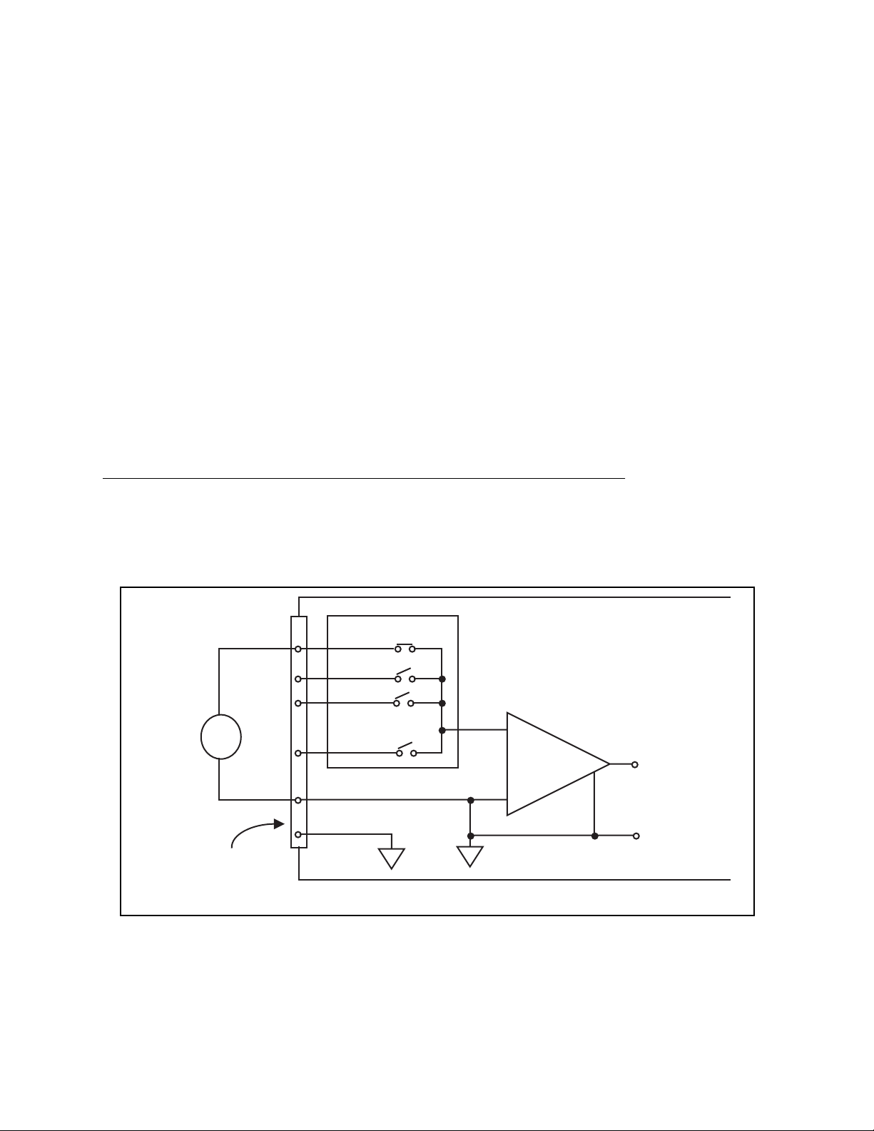
How you connect analog input signals to the DAQPad-1200 depends on how you configure the
DAQPad-1200 analog input circuitry and the type of input signal source. With different
DAQPad-1200 configurations, you can use the DAQPad-1200 instrumentation amplifier in
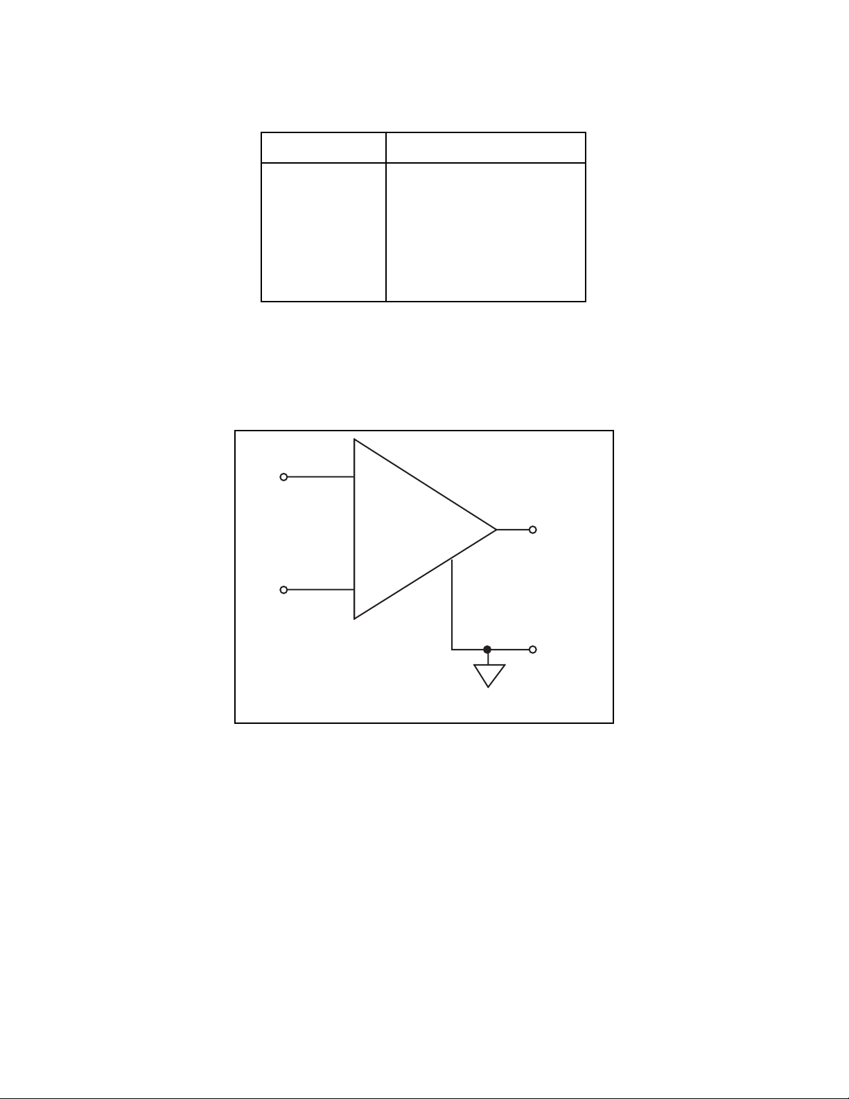
different ways. Figure 3-2 shows a diagram of the DAQPad-1200 instrumentation amplifier.
Instrumentation
+
V
in
+
Amplifier
+
V
Measured
m
Voltage
-
V
= [V
m
-
in
+
- V
-
] * GAIN
in
V
-
in
Figure 3-2. DAQPad-1200 Instrumentation Amplifier
The DAQPad-1200 instrumentation amplifier applies gain, common-mode voltage rejection, and
high-input impedance to the analog input signals connected to the DAQPad-1200 unit. Signals
are routed to the positive and negative inputs of the instrumentation amplifier through input
multiplexers on the DAQPad-1200. The instrumentation amplifier converts two input signals to
a signal that is the difference between the two input signals multiplied by the gain setting of the
amplifier. The amplifier output voltage is referenced to the DAQPad-1200 ground. The
DAQPad-1200 ADC measures this output voltage when it performs A/D conversions.
All signals must be referenced to ground, either at the source device or at the DAQPad-1200. If
you have a floating source, you must use a ground-referenced input connection at the
DAQPad-1200. If you have a grounded source, you must use a nonreferenced input connection
at the DAQPad-1200.
© National Instruments Corporation 3-5 DAQPad-1200 User Manual
Page 25

Signal Connections Chapter 3
Types of Signal Sources
When configuring the input mode of the DAQPad-1200 and making signal connections, you
must first determine whether the signal source is floating or ground referenced. These two types
of signals are described as follows.
Floating Signal Sources
A floating signal source is not connected in any way to the building ground system but has an
isolated ground-reference point. Some examples of floating signal sources are outputs of
transformers, thermocouples, battery-powered devices, optical isolator outputs, and isolation
amplifiers. You must tie the ground reference of a floating signal to the DAQPad-1200 analog
input ground to establish a local or onboard reference for the signal. Otherwise, the measured
input signal varies or appears to float. An instrument or device that supplies an isolated output
falls into the floating signal source category.
Ground-Referenced Signal Sources
A ground-referenced signal source is connected in some way to the building system ground and
is therefore already connected to a common ground point with respect to the DAQPad-1200,
assuming that the PC is plugged into the same power system. Nonisolated outputs of instruments
and devices that plug into the building power system fall into this category.
The difference in ground potential between two instruments connected to the same building
power system is typically between 1 mV and 100 mV but can be much higher if power
distribution circuits are not properly connected. The connection instructions that follow for
grounded signal sources eliminate this ground potential difference from the measured signal.
Note: If you power both the DAQPad-1200 and your PC with a floating power source (such
as a battery), then your system may be floating with respect to earth ground. In this
case, treat all of your signal sources as floating sources.
Input Configurations
You can configure the DAQPad-1200 for one of three input modes—RSE, NRSE, or DIFF. The
following sections discuss the use of single-ended and differential measurements, and
considerations for measuring both floating and ground-referenced signal sources. Figure 3-3
summarizes the recommended input configurations for both types of signal sources.
DAQPad-1200 User Manual 3-6 © National Instruments Corporation
Page 26

Chapter 3 Signal Connections
Signal Source Type
Input
Differential
(DIFF)
Single-Ended —
Ground
Referenced
(RSE)
Floating Signal Source
(Not Connected to Building Ground)
Examples
• Ungrounded Thermocouples
• Signal conditioning with isolated outputs
• Battery devices
+
V
1
-
ACH(+)
ACH (-)
R
+
-
AIGND
See text for information on bias resistors.
+
V
1
-
ACH
AIGND
+
-
Grounded Signal Source
Examples
• Plug-in instruments with
nonisolated outputs
+
V
1
-
NOT RECOMMENDED
+
V
1
-
+ Vg -
ACH(+)
ACH (-)
ACH
+
-
AIGND
+
-
Ground-loop losses, Vg, are added to
measured signal
Single-Ended —
Nonreferenced
(NRSE)
+
V
1
-
ACH
AISENSE
+
-
R
AIGND
+
V
1
-
ACH
AISENSE
+
-
AIGND
See text for information on bias resistors.
Figure 3-3. Summary of Analog Input Connections
© National Instruments Corporation 3-7 DAQPad-1200 User Manual
Page 27

Signal Connections Chapter 3
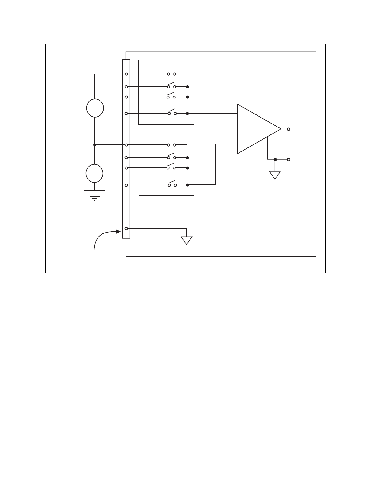
Differential Connection Considerations (DIFF Configuration)
Differential connections are those in which each DAQPad-1200 analog input signal has its own
reference signal or signal return path. These connections are available when you configure the
DAQPad-1200 in the DIFF mode. Each input signal is tied to the positive input of the
instrumentation amplifier, and its reference signal, or return, is tied to the negative input of the
instrumentation amplifier.
When you configure the DAQPad-1200 for DIFF input, each signal uses two of the multiplexer
inputs—one for the signal and one for its reference signal. Therefore, only four analog input
channels are available when using the DIFF configuration. You should use the DIFF input
configuration when any of the following conditions are present:
• Input signals are low level (less than 1 V).
• Leads connecting the signals to the DAQPad-1200 are greater than 15 ft.
• Any of the input signals requires a separate ground-reference point or return signal.
• The signal leads travel through noisy environments.
Differential signal connections reduce picked-up noise and increase common-mode signal and
noise rejection. With these connections, input signals can float within the common-mode limits
of the input instrumentation amplifier.
Differential Connections for Grounded Signal Sources
Figure 3-4 shows how to connect a ground-referenced signal source to a DAQPad-1200 unit
configured for DIFF input. Configuration instructions are included in the Analog I/O
Configuration section in Chapter 2, Installation and Configuration.
DAQPad-1200 User Manual 3-8 © National Instruments Corporation
Page 28
Chapter 3 Signal Connections
ACH 0
1
ACH 2
3
ACH 4
5
7
ACH 6
+
Grounded
Signal
Source
+
V
s
-
V
m
+
Measured
Voltage
-
CommonMode
Noise,
Ground
Potential,
and so on
Front I/O Connector
V
cm
ACH 1
2
ACH 3
4
+
-
6
8
11
ACH 5
ACH 7
AGND
DAQPad-1200 Unit in DIFF Configuration
-
Figure 3-4. Differential Input Connections for Grounded Signal Sources
With this type of connection, the instrumentation amplifier rejects both the common-mode noise
in the signal and the ground-potential difference between the signal source and the
DAQPad-1200 ground (shown as V
in Figure 3-4).
CM
Differential Connections for Floating Signal Sources
Figure 3-5 shows how to connect a floating signal source to a DAQPad-1200 unit that is
configured for DIFF input. Configuration instructions are included in the Analog I/O
Configuration section of Chapter 2, Installation and Configuration.
© National Instruments Corporation 3-9 DAQPad-1200 User Manual
Page 29

Signal Connections Chapter 3
ACH 0
1
ACH 2
3
ACH 4
Floating
Signal
Source
+
V
s
-
5
7
ACH 6
+
V
m
+
Measured
Voltage
-
100 kΩ
Bias
Current
Return
Paths
Front I/O Connector
100 kΩ
2
4
6
8
11
ACH 1
ACH 3
ACH 5
ACH 7
AGND
-
DAQPad-1200 Unit in DIFF Configuration
Figure 3-5. Differential Input Connections for Floating Sources
The 100 kΩ resistors shown in Figure 3-5 create a return path to ground for the bias currents of
the instrumentation amplifier. If there is no return path, the instrumentation amplifier bias
currents charge stray capacitances, resulting in uncontrollable drift and possible saturation in the
amplifier. Typically, values from 10 to 100 kΩ are used.
A resistor from each input to ground, as shown in Figure 3-5, provides bias current return paths
for an AC-coupled input signal.
If the input signal is DC-coupled, you need only the resistor that connects the negative signal
input to ground. This connection does not lower the input impedance of the analog input
channel.
Single-Ended Connection Considerations
Single-ended connections are those in which all DAQPad-1200 analog input signals are
referenced to one common ground. The input signals are tied to the positive input of the
instrumentation amplifier, and their common ground point is tied to the negative input of the
instrumentation amplifier.
DAQPad-1200 User Manual 3-10 © National Instruments Corporation
Page 30
Chapter 3 Signal Connections
When the DAQPad-1200 is configured for single-ended input (NRSE or RSE), eight analog
input channels are available. You can use single-ended input connections when the following
criteria are met by all input signals:
1. Input signals are high level (greater than 1 V).
2. Leads connecting the signals to the DAQPad-1200 are less than 15 ft.
3. All input signals share a common reference signal (at the source).
If any of the preceding criteria are not met, using DIFF input configuration is recommended.
You can software configure the DAQPad-1200 for two different types of single-ended
connections, RSE configuration and NRSE configuration. Use the RSE configuration for
floating signal sources; in this case, the DAQPad-1200 provides the reference ground point for
the external signal. Use the NRSE configuration for ground-referenced signal sources; in this
case, the external signal supplies its own reference ground point and the DAQPad-1200 should
not supply one.
Single-Ended Connections for Floating Signal Sources (RSE Configuration)
Figure 3-6 shows how to connect a floating signal source to a DAQPad-1200 unit configured for
single-ended input. You must configure the DAQPad-1200 analog input circuitry for RSE input
to make these types of connections. Configuration instructions are included in the Analog I/O
Configuration section of Chapter 2, Installation and Configuration.
ACH 0
1
ACH 1
2
ACH 2
3
Floating
Signal
Source
Front I/O Connector
+
V
s
-
ACH 7
8
AISENSE/AIGND
9
AGND
11
DAQPad-1200 Unit in RSE Configuration
+
+
m
Measured
Voltage
-
-
V
Figure 3-6. Single-Ended Input Connections for Floating Signal Sources
© National Instruments Corporation 3-11 DAQPad-1200 User Manual
Page 31

Signal Connections Chapter 3
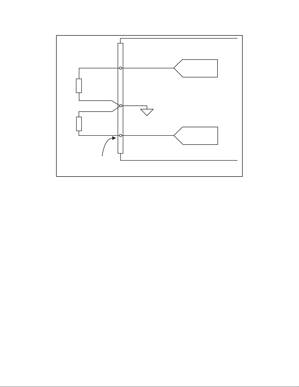
Single-Ended Connections for Grounded Signal Sources (NRSE Configuration)
If you measure a grounded signal source with a single-ended configuration, you must configure
the DAQPad-1200 in the NRSE input configuration. The signal is connected to the positive
input of the DAQPad-1200 instrumentation amplifier and the signal local ground reference is
connected to the negative input of the DAQPad-1200 instrumentation amplifier. Therefore, you
must connect the ground point of the signal to the AISENSE pin. Any potential difference
between the DAQPad-1200 ground and the signal ground appears as a common-mode signal at
both the positive and negative inputs of the instrumentation amplifier and is therefore rejected by
the amplifier. On the other hand, if the input circuitry of the DAQPad-1200 is referenced to
ground, such as in the RSE configuration, this difference in ground potentials appears as an error
in the measured voltage.
Figure 3-7 shows how to connect a grounded signal source to a DAQPad-1200 unit configured in
the NRSE configuration. Configuration instructions are included in the Analog I/O
Configuration section in Chapter 2, Installation and Configuration.
1
ACH 0
ACH 1
2
ACH 2
Ground-
Referenced
Signal
Source
Common-
Mode
Noise
and so on
Front I/O Connector
+
V
s
-
+
V
cm
-
3
8
9
11
ACH 7
AISENSE/AIGND
AGND
DAQPad-1200 Unit in NRSE Input Configuration
+
-
V
m
+
Measured
Voltage
-
Figure 3-7. Single-Ended Input Connections for Grounded Signal Sources Common-Mode Signal Rejection Considerations Figures 3-4 and 3-7 show connections for signal sources that are already referenced to some
ground point with respect to the DAQPad-1200. In these cases, the instrumentation amplifier
can reject any voltage caused by ground-potential differences between the signal source and the
DAQPad-1200. In addition, with differential input connections, the instrumentation amplifier
can reject common-mode noise pickup in the leads connecting the signal sources to the
DAQPad-1200.
DAQPad-1200 User Manual 3-12 © National Instruments Corporation
Page 32

Chapter 3 Signal Connections
The common-mode input range of the DAQPad-1200 instrumentation amplifier is the magnitude
of the greatest common-mode signal that can be rejected.
The common-mode input range for the DAQPad-1200 depends on the size of the differential
input signal (V
diff
= V
+
in
-
- V
)and the gain setting of the instrumentation amplifier. In unipolar
in
mode, the differential input range is 0 to 10 V. In bipolar mode, the differential input range is
-5 to +5 V. Inputs should remain within a range of -5 to 10 V in both bipolar and unipolar
modes.
Analog Output Signal Connections
Pins 10 through 12 of the front connector are analog output signal pins.
Pins 10 and 12 are the DAC0OUT and DAC1OUT signal pins. DAC0OUT is the voltage output
signal for analog output channel 0. DAC1OUT is the voltage output signal for analog output
channel 1.
Pin 11, AGND, is the ground-reference point for both analog output channels as well as analog
input.
The following output ranges are available:
• Output signal range
– Bipolar output ±5 V
– Unipolar output 0 to 10 V
*
Maximum load current ±2 mA for 12-bit linearity.
*
*
Figure 3-8 shows how to make analog output signal connections.
© National Instruments Corporation 3-13 DAQPad-1200 User Manual
Page 33
Signal Connections Chapter 3
+
Load
Load
Front I/O Connector
VOUT 0
-
-
VOUT 1
+
Figure 3-8. Analog Output Signal Connections
Digital I/O Signal Connections
10 DAC0OUT
AGND
11
12
DAC1OUT
Channel 0
Channel 1
Analog Output Channels
DAQPad-1200 Unit
Pins 13 through 37 of the front connector are digital I/O signal pins. Digital I/O on the
DAQPad-1200 uses the 82C55A integrated circuit. The 82C55A is a general-purpose peripheral
interface containing 24 programmable I/O pins. These pins represent the three 8-bit ports
(PA, PB, and PC) of the 82C55A.
Pins 14 through 21 are connected to the digital lines PA<0..7> for digital I/O port A. Pins 22
through 29 are connected to the digital lines PB<0..7> for digital I/O port B. Pins 30 through 37
are connected to the digital lines PC<0..7> for digital I/O port C. Pin 13, DGND, is the digital
ground pin for all three digital I/O ports. Refer to Appendix A, Specifications, for signal voltage
and current specifications.
DAQPad-1200 User Manual 3-14 © National Instruments Corporation
Page 34

Chapter 3 Signal Connections
Figure 3-9 illustrates signal connections for three typical digital I/O applications.
+5 V
LED
+5 V
TTL Signal
Switch
Front I/O Connector
14 PA0
Port A
P A<7..0>
Port B
22 PB0
PB<7..0>
30 PC0
Port C
PC<7..0>
13
DGND
DAQPad-1200 Unit
Figure 3-9. Digital I/O Connections
In Figure 3-9, port A is configured for digital output, and ports B and C are configured for digital
input. Digital input applications include receiving TTL signals and sensing external device states
such as the switch in Figure 3-9. Digital output applications include sending TTL signals and
driving external devices such as the LED shown in Figure 3-9.
© National Instruments Corporation 3-15 DAQPad-1200 User Manual
Page 35

Signal Connections Chapter 3
Port C Pin Connections
The signals assigned to port C depend on the mode in which the 82C55A is programmed. In
mode 0, port C is considered to be two 4-bit I/O ports. In modes 1 and 2, port C is used for
status and handshaking signals with two or three I/O bits mixed in. Table 3-3 summarizes the
signal assignments of port C for each programmable mode. See your DAQPad-1200 Register-
Level Programmer Manual for programming information.
Table 3-3. Port C Signal Assignments
Programmable Mode Group A Group B
PC7 PC6 PC5 PC4 PC3 PC2 PC1 PC0
Mode 0
Mode 1 Input
Mode 1 Output
Mode 2
*Indicates that the signal is active low.
I/O I/O I/O I/O I/O I/O I/O I/O
I/O I/O IBF
OBFA* ACKA* I/O I/O INTR
OBFA* ACKA* IBF
STBA* INTR
A
STBA* INTR
A
STBB* IBFB
A
ACKB* OBFB* INTR
A
I/O I/O I/O
A
INTR
B
Timing Specifications
Use the handshaking lines STB* and IBF to synchronize input transfers. Use the handshaking
lines OBF* and ACK* to synchronize output transfers.
The following signals are used in the timing diagrams shown later in this chapter:
Name Type Description
STB* Input Strobe Input—A low signal on this handshaking line loads data into the input latch.
IBF Output Input Buffer Full—A high signal on this handshaking line indicates that data has
been loaded into the input latch. This is primarily an input acknowledge signal.
ACK* Input Acknowledge Input—A low signal on this handshaking line indicates that the data
written from the specified port has been accepted. This signal is primarily a
response from the external device that it has received the data from the
DAQPad-1200.
OBF* Output Output Buffer Full—A low signal on this handshaking line indicates that data has
been written from the specified port.
INTR Output Interrupt Request—This signal becomes high when the 82C55A is requesting
service during a data transfer. Set the appropriate interrupt enable signals to
generate this signal.
RD* Internal Read Signal—This signal is the read signal generated from the parallel port interface
circuitry.
WRT* Internal Write Signal—This signal is the write signal generated from the parallel port
interface circuitry.
DATA Bidirectional Data Lines at the Specified Port—This signal indicates when the data on the data
lines at a specified port is or should be available.
B
B
DAQPad-1200 User Manual 3-16 © National Instruments Corporation
Page 36
Chapter 3 Signal Connections
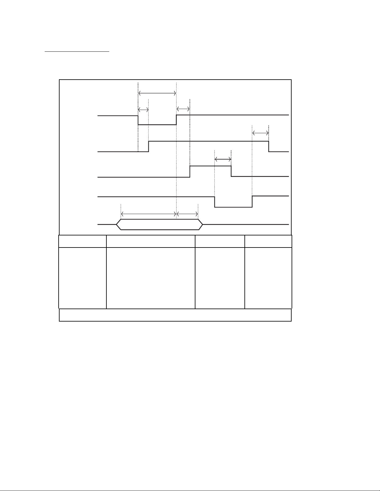
Mode 1 Input Timing
The timing specifications for an input transfer in mode 1 are as follows:
T1
T2 T4
STB *
T7
IBF
T6
INTR
RD *
T3 T5
DATA
Name Description Minimum Maximum
T1 STB* pulse width 500 –
T2 STB* = 0 to IBF = 1 – 300
T3 Data before STB*= 1 0 –
T4 STB* = 1 to INTR = 1 – 300
T5 Data after STB* = 1 180 –
T6 RD* = 0 to INTR = 0 – 400
T7 RD* = 1 to IBF = 0 – 300
All timing values are in nanoseconds.
Figure 3-10. Mode 1 Timing Specifications for Input Transfers
© National Instruments Corporation 3-17 DAQPad-1200 User Manual
Page 37
Signal Connections Chapter 3
Mode 1 Output Timing
The timing specifications for an output transfer in mode 1 are as follows:
T3
WRT*
T4
OBF*
INTR
ACK*
DATA
T1
T6
T5
T2
Name Description Minimum Maximum
T1 WRT* = 0 to INTR = 0 – 450
T2 WRT* = 1 to output – 350
T3 WRT* = 1 to OBF* = 0 – 650
T4 ACK* = 0 to OBF* = 1 – 350
T5 ACK* pulse width 300 –
T6 ACK* = 1 to INTR = 1 – 350
All timing values are in nanoseconds.
Figure 3-11. Mode 1 Timing Specifications for Output Transfers
DAQPad-1200 User Manual 3-18 © National Instruments Corporation
Page 38

Chapter 3 Signal Connections
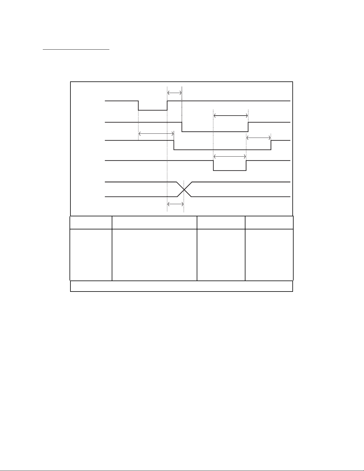
Mode 2 Bidirectional Timing
The timing specifications for bidirectional transfers in mode 2 are as follows:
T1
WRT *
OBF *
INTR
ACK *
STB *
IBF
RD *
DATA
T3
T4
T2 T5 T8 T9
T6
T7
Name Description Minimum Maximum
T1 WRT* = 1 to OBF* = 0 – 650
T2 Data before STB*= 1 0 –
T3 STB* pulse width 500 –
T4 STB* = 0 to IBF = 1 – 300
T5 Data after STB* = 1 180 –
T6 ACK* = 0 to OBF = 1 – 350
T7 ACK* pulse width 300 –
T8 ACK* = 0 to output – 300
T9 ACK* = 1 to output float 20 250
T10 RD* = 1 to IBF = 0 – 300
T10
All timing values are in nanoseconds.
Figure 3-12. Mode 2 Timing Specification for Bidirectional Transfers
DAQ and General-Purpose Timing Signal Connections
Pins 38 through 48 of the front connector are connections for timing I/O signals. The
DAQPad-1200 timing I/O uses two 82C53 counter/timer integrated circuits. One circuit,
designated 82C53(A), is used exclusively for DAQ timing, and the other, 82C53(B), is available
for general use. You can use pins 38 through 40 and pin 43 to carry external signals for DAQ
timing in place of the dedicated 82C53(A). These signals are explained in the next section, DAQ
Timing Connections. Pins 41 through 48 carry general-purpose timing signals from 82C53(B).
These signals are explained in the General-Purpose Timing Signal Connections section later in
this chapter.
© National Instruments Corporation 3-19 DAQPad-1200 User Manual
Page 39

Signal Connections Chapter 3
DAQ Timing Connections
Each 82C53 counter/timer circuit contains three counters. Counter 0 on the 82C53(A)
counter/timer (referred to as A0) is a sample-interval counter in timed A/D conversions.
Counter 1 on the 82C53(A) counter/timer (referred to as A1) is a sample counter in controlled
A/D conversions. Therefore, counter A1 stops data acquisition after a predefined number of
samples. These counters are not available for general use.
Instead of counter A0, you can use EXTCONV* to externally time conversions. Figure 3-13
shows the timing requirements for the EXTCONV* input. An A/D conversion is initiated by a
falling edge on the EXTCONV*.
t
w
tw 250 ns minimum
EXTCONV*
V
IH
t
V
IL
w
A/D Conversion starts within
125 ns from this point.
Figure 3-13. EXTCONV* Signal Timing
The external control signal EXTTRIG can either start a DAQ sequence or terminate an ongoing
DAQ sequence depending on the mode—Posttrigger (POSTTRIG) or Pretrigger (PRETRIG).
These modes are software selectable.
In the POSTTRIG mode, EXTTRIG serves as an external trigger that initiates a DAQ sequence.
When you use counter A0 to time sample intervals, a rising edge on EXTTRIG starts counter A0
and the DAQ sequence. When you use EXTCONV* to time sample intervals, data acquisition is
enabled on a rising edge of EXTTRIG followed by a rising edge on EXTCONV*. The first
conversion occurs on the next falling edge of EXTCONV*. Further transitions on the EXTTRIG
line have no effect until a new DAQ sequence is established.
Figure 3-14 shows a possible controlled DAQ sequence using EXTCONV* and EXTTRIG. The
rising edge of EXTCONV* that enables external conversions must occur a minimum of 50 ns
after the rising edge of EXTTRIG. The first conversion occurs on the next falling edge of
EXTCONV*.
DAQPad-1200 User Manual 3-20 © National Instruments Corporation
Page 40

Chapter 3 Signal Connections
t
EXTTRIG
EXTCONV*
CONVERT
w
V
IH
t
w
V
IL
t
d
tw 50 ns minimum
td 50 ns minimum
Figure 3-14. Posttrigger DAQ Timing
In the PRETRIG mode, EXTTRIG serves as a stop-trigger signal. Data is acquired both before
and after the stop trigger occurs. A/D conversions are software enabled, which initiates the DAQ
operation. However, the sample counter is not started until a rising edge is sensed on the
EXTTRIG input. Conversions remain enabled until the sample counter counts to zero. The
maximum number of samples acquired after the stop trigger is limited to 65,535. The number of
samples acquired before the trigger is limited only by the size of the memory buffer available for
data acquisition.
Figure 3-15 shows a pretrigger DAQ timing sequence using EXTTRIG and EXTCONV*. The
DAQ operation has been initiated through software. Notice that the sample counter has been
programmed to allow five conversions after the rising edge on the EXTTRIG signal. Additional
transitions on the EXTTRIG line have no effect until you initiate a new DAQ sequence.
t
w
V
EXTTRIG
EXTCONV*
CONVERT
IH
t
w
V
IL
tw 50 ns minimum
Figure 3-15. Pretrigger DAQ Timing
© National Instruments Corporation 3-21 DAQPad-1200 User Manual
Page 41

Signal Connections Chapter 3
Because both pretrigger and posttrigger modes use EXTTRIG input, you can only use one mode
at a time.
For interval scanning data acquisition, counter B1 determines the scan interval. Instead of using
counter B1, you can externally time the scan interval through OUTB1. If you externally time the
sample interval, we recommend that you also externally time the scan interval.
Figure 3-16 shows an example of a multiple-channel interval-scanning DAQ operation. The
scan interval and the sample interval are being timed externally through OUTB1 and
EXTCONV*. Channels 1 and 0 of the input multiplexers are being scanned once during each
scan interval. The first rising edge of EXTCONV* must occur a minimum of 50 ns after the
rising edge on OUTB1. The first rising edge of EXTCONV* after the rising edge of OUTB1
enables an internal GATE signal that allows conversions to occur. The first conversion then
occurs on the following falling edge of EXTCONV*.
OUTB1
tw = 50 ns
td = 50 ns
EXTCONV*
CONVERT
GATE
ADC CH
CH1 CH0
CH1
CH0
Figure 3-16. Interval-Scanning Signal Timing
You use the final external control signal, EXTUPDATE*, to externally control updating the
output voltage of the 12-bit DACs and/or to generate an externally timed interrupt. There are
two update modes, immediate update and delayed update. In immediate update mode the analog
output is updated as soon as a value is written to the DAC. If you select the delayed update
mode, a value is written to the DAC; however, the corresponding DAC voltage is not updated
until a low level on the EXTUPDATE* signal is sensed. Furthermore, if you enable interrupt
generation, an interrupt is generated whenever a rising edge is detected on the EXTUPDATE*
bit. Therefore, you can perform externally timed interrupt-driven waveform generation on the
DAQPad-1200.
Figure 3-17 illustrates a waveform generation timing sequence using the EXTUPDATE* signal
and the delayed update mode. The DACs are updated by a high level on the DAC OUTPUT
UPDATE signal, which in this case is triggered by a low level on the EXTUPDATE* line.
CNTINT is the signal that interrupts the PC. This interrupt is generated on the rising edge of
EXTUPDATE*. DACWRT is the signal that writes a new value to the DAC.
DAQPad-1200 User Manual 3-22 © National Instruments Corporation
Page 42
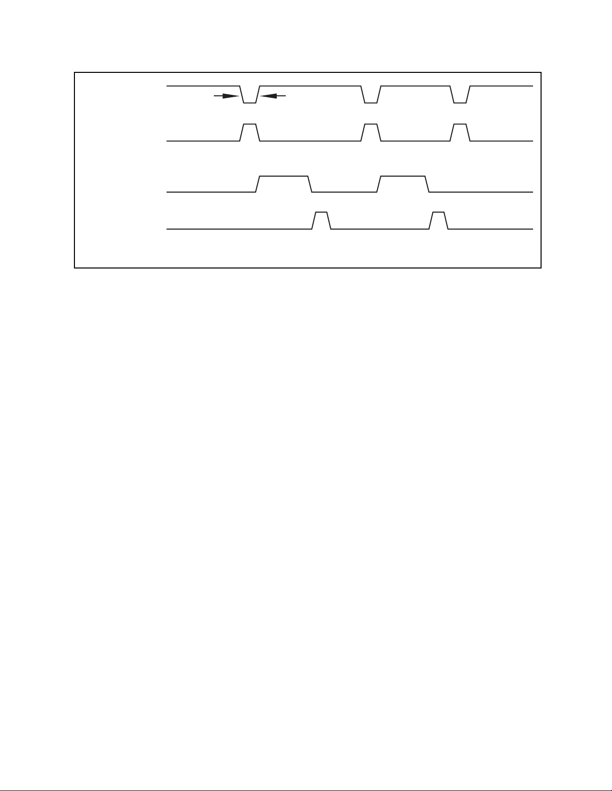
Chapter 3 Signal Connections
EXTUPDATE*
t
w
DAC OUTPUT
UPDATE
CNTINT
DACWRT
tw Minimum 50 ns
Figure 3-17. EXTUPDATE* Signal Timing for Updating DAC Output
The following rating applies to the EXTCONV*, EXTTRIG, OUTB1, and EXTUPDATE*
signals.
• Absolute maximum voltage input rating -0.5 to 7.0 V with respect to DGND
For more information concerning the various modes of data acquisition and analog output, refer
to your NI-DAQ manual or to Chapter 2, Theory of Operation, in the DAQPad-1200 Register-
Level Programmer Manual.
General-Purpose Timing Signal Connections
The general-purpose timing signals include the GATE, CLK, and OUT signals for the three
82C53(B) counters. The 82C53 counter/timers can be used for general-purpose applications
such as pulse and square wave generation; event counting; and pulse-width, time-lapse, and
frequency measurement. For these applications, the CLK and GATE signals at the front I/O
connector control the counters. The single exception is counter B0, which has an internal 2 MHz
clock. Refer to the DAQPad-1200 Register-Level Programmer Manual for programming
information.
You perform pulse and square wave generation by programming a counter to generate a timing
signal at its OUT output pin. You perform event counting by programming a counter to count
rising or falling edges applied to any of the 82C53 CLK inputs. You can then read the counter
value to determine the number of edges that have occurred. You can gate counter operations on
and off during event counting. Figure 3-18 shows connections for a typical event-counting
operation in which a switch is used to gate the counter on and off.
© National Instruments Corporation 3-23 DAQPad-1200 User Manual
Page 43

Signal Connections Chapter 3
+5 V
10 kΩ
CLK
OUT
GATE
Signal
Source
Switch
Counter (from Group B)
13
I/O Connector
DGND
DAQPad-1200 Unit
Figure 3-18. Event-Counting Application with External Switch Gating
Pulse-width measurement is performed by level gating. The pulse you want to measure is
applied to the counter GATE input. The counter is loaded with the known count and is
programmed to count down while the signal at the GATE input is high. The pulse width equals
the counter difference (loaded value minus read value) multiplied by the CLK period.
Perform time-lapse measurement by programming a counter to be edge gated. An edge is
applied to the counter GATE input to start the counter. You can program the counter to start
counting after receiving a low-to-high edge. The time lapse since receiving the edge equals the
counter value difference (loaded value minus read value) multiplied by the CLK period.
To perform frequency measurement, program a counter to be level gated and count the number
of falling edges in a signal applied to a CLK input. The gate signal applied to the counter GATE
input is of known duration. In this case, you program the counter to count falling edges at the
CLK input while the gate is applied. The frequency of the input signal then equals the count
value divided by the gate period. Figure 3-19 shows the connections for a frequency
measurement application. You can also use a second counter to generate the gate signal in this
application. In this case, program the second counter for a one-shot mode, which requires an
external inverter to make the output pulse of the second counter active high.
DAQPad-1200 User Manual 3-24 © National Instruments Corporation
Page 44

Chapter 3 Signal Connections
+5 V
10 kΩ
CLK
OUT
GATE
Signal
Source
I/O Connector
Gate
Source
13
Counter
DGND
DAQPad-1200 Unit
Figure 3-19. Frequency Measurement Application
The GATE, CLK, and OUT signals for counters B1 and B2 are available at the I/O front
connector. The GATE and CLK pins are internally pulled up to +5 V through a 10 kΩ resistor.
Refer to Appendix A, Specifications, for signal voltage and current specifications.
© National Instruments Corporation 3-25 DAQPad-1200 User Manual
Page 45
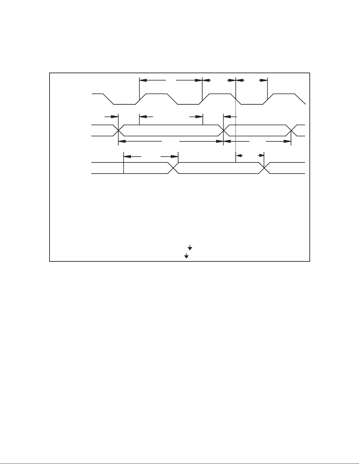
Signal Connections Chapter 3
Figure 3-20 shows the timing requirements for the GATE and CLK input signals and the timing
specifications for the OUT output signals of the 82C53.
CLK
GATE
OUT
t
sc
V
IH
V
IL
t
gsu
V
IH
V
IL
t
V
OH
V
OL
t
sc
t
pwh
t
pwl
t
gsu
t
gh
t
gwh
t
gwl
t
outg
t
outc
clock period
clock high level
clock low level
gate setup time
gate hold time
gate high level
gate low level
output delay from clock
output delay from gate
outg
t
gwh
t
pwh
t
gh
t
380 ns minimum
230 ns minimum
150 ns minimum
100 ns minimum
50 ns minimum
150 ns minimum
100 ns minimum
300 ns maximum
400 ns maximum
t
pwl
outc
t
gwl
Figure 3-20. General-Purpose Timing Signals
The GATE and OUT signals in Figure 3-20 are referenced to the rising edge of the CLK signal.
Power Connections
Pin 49 of the I/O connector supplies +5 V from the DAQPad-1200 power supply. This pin is
referenced to DGND and you can use the +5 V to power external digital circuitry.
• Power rating 400 mA at +5 V max
Warning: Do not directly connect this +5 V power pin to any other voltage source on the
DAQPad-1200 or any other device. Doing so can damage the DAQPad-1200 or
your PC. National Instruments is
power connections.
DAQPad-1200 User Manual 3-26 © National Instruments Corporation
NOT liable for any damage due to incorrect
Page 46

Chapter 3 Signal Connections
Pin 49 is fused for up to 400 mA. Shorting pin 49 to a ground will not damage the
DAQPad-1200. If you do not receive +5 V from pin 49 of the I/O connector, make sure that the
front panel rocker switch is turned on and check for any shorts between the +5 V power pin and
ground.
Note: You can replace a blown fuse with the spare fuse located on the printed wire board by
removing the two rear panel screws. However, we recommend that you contact
National Instruments. The DAQPad-1200 uses a 400 mA, 63 V quick-acting surface
mount fuse from Schurter.
Field Wiring Considerations
Environmental noise can seriously affect the accuracy of measurements made with your
DAQPad-1200 if you do not take proper care when running signal wires between signal sources
and the board. The following recommendations apply mainly to analog input signal routing to
the board, although they also apply to signal routing in general.
You can minimize noise pickup and maximize measurement accuracy by taking the following
precautions:
• Use differential analog input connections to reject common-mode noise.
• Use individually shielded, twisted-pair wires to connect analog input signals to the
DAQPad-1200. With this type of wire, the signals attached to the ACH+ and ACH- inputs
are twisted together and then covered with a shield. You then connect this shield only at one
point to the signal source ground. This kind of connection is required for signals traveling
through areas with large magnetic fields or high electromagnetic interference.
• Route signals to the board carefully. Keep cabling away from noise sources. The most
common noise source in a PC data acquisition system is the video monitor. Separate the
monitor from the analog signals as much as possible.
The following recommendations apply for all signal connections to your DAQPad-1200:
• Separate DAQPad-1200 signal lines from high-current or high-voltage lines. These lines are
capable of inducing currents in or voltages on the DAQPad-1200 signal lines if they run in
parallel paths at a close distance. To reduce the magnetic coupling between lines, separate
them by a reasonable distance if they run in parallel, or run the lines at right angles to each
other.
• Do not run signal lines through conduits that also contain power lines.
• Protect signal lines from magnetic fields caused by electric motors, welding equipment,
breakers, or transformers by running them through special metal conduits.
© National Instruments Corporation 3-27 DAQPad-1200 User Manual
Page 47

Chapter 4 Calibration
This chapter discusses the calibration procedures for the DAQPad-1200 analog I/O circuitry.
However, the DAQPad-1200 is factory calibrated, and National Instruments can recalibrate your
unit if needed. To maintain the 12-bit accuracy of the DAQPad-1200 analog input and analog
output circuitry, recalibrate at 6 month intervals.
There are three ways to perform calibrations.
• Use the NI-DAQ SCXI_1200_Calibrate function. (This function is also used for the
SCXI-1200 module, which is functionally equivalent to the DAQPad-1200.) This is the
simplest method.
• Use the NI-DAQ functions to write to the calibration DACs and the EEPROM.
• Use your own register-level writes to the calibration DACs and the EEPROM.
To accomplish calibration using the last two methods, you need to know the details of the
calibration process. This information is in the Theory of Operation chapter of the DAQPad-1200
Register-Level Programmer Manual.
The DAQPad-1200 is software calibrated, therefore there are no calibration trimpots. The unit is
shipped with a utility software for calibration. The calibration process involves reading offset
and gain errors from the analog input and analog output sections and writing values to the
appropriate calibration DACs to null the errors. There are four calibration DACs associated with
the analog input section and four calibration DACs associated with the analog output section,
two for each output channel. After the calibration process is complete, each calibration DAC is
at a known value. Because these values are lost when the board is powered down, they are also
stored in the onboard EEPROM for future reference.
The factory information occupies one half of the EEPROM and is write protected. The lower
half of the EEPROM contains user areas for calibration data. There are six different user areas.
When the DAQPad-1200 is powered on, or the conditions under which it is operating change,
you must load the calibration DACs with the appropriate calibration constants.
If you use the DAQPad-1200 with NI-DAQ and LabVIEW or LabWindows/CVI, the factory
calibration constants are automatically loaded into the calibration DAC the first time a function
pertaining to the DAQPad-1200 is called, and then each time you change your configuration
(which includes gain). You can instead choose to load the calibration DACs with calibration
constants from the user areas in the EEPROM or you can recalibrate the DAQPad-1200 and load
these constants directly into the calibration DACs. Calibration software is included with the
DAQPad-1200 as part of the NI-DAQ software.
© National Instruments Corporation 4-1 DAQPad-1200 User Manual
Page 48

Calibration Chapter 4
Calibration at Higher Gains
The DAQPad-1200 has a maximum gain error of 0.5%. This means that if the board is
calibrated at a gain of 1, and if the gain is switched to 100, a maximum of 50 mV error may
result in the reading. Therefore, when you are recalibrating the DAQPad-1200, you should
perform gain calibration at all other gains (2, 5, 10, 20, 50, and 100), and store the corresponding
values in the user gain calibration data area of the EEPROM, thus ensuring a maximum error of
0.02 % at all gains.
Calibration Equipment Requirements
The equipment you use to calibrate the DAQPad-1200 should have a ±0.001% rated accuracy,
which is 10 times as accurate as the DAQPad-1200. However, calibration with only four times
the accuracy as the DAQPad-1200 and a ±0.003% rated accuracy are acceptable. The inaccuracy
of the calibration equipment results only in gain error; offset error is unaffected.
Calibrate the DAQPad-1200 to a measurement accuracy of ±0.5 LSBs, which is within ±0.012%
of its input range.
For analog input calibration, use a precision DC voltage source, such as a calibrator, with the
following specifications.
Voltage 0 to 10 V
Accuracy ±0.001% standard
±0.003% acceptable
Using the Calibration Function
NI-DAQ contains the SCXI_1200_Calibrate function, with which you can either load the
calibration DACs with the factory constants or the user defined constants stored in the
EEPROM, or perform your own calibration and directly load these constants into the calibration
DACs. To use the SCXI_1200_Calibrate function for analog input calibration, you must
ground an analog input channel at the front connector (for offset calibration) and apply an
accurate voltage reference to another input channel (for gain calibration). For analog output
calibration, the DAC0 and DAC1 outputs must be wrapped back and applied to two other analog
input channels.
When you perform analog input calibration, you must first configure the ADC for referenced
single-ended (RSE) mode and for the correct polarity at which you want to perform data
acquisition. When you perform analog output calibration, you must first configure the analog
input circuitry for RSE and for bipolar polarity, and you must configure the analog output
circuitry for the correct polarity at which you want to perform output waveform generation.
Refer to the NI-DAQ User Manual for PC Compatibles for more details on the
SCXI_1200_Calibrate function.
DAQPad-1200 User Manual 4-2 © National Instruments Corporation
Page 49

Appendix A Specifications
This appendix lists the specifications of the DAQPad-1200. These specifications are typical at
25° C unless otherwise stated. The operating temperature range is 0° to 50° C.
Analog Input
Input Characteristics
Number of channels Eight single-ended, four differential, software
selectable
Type of ADC Successive approximation
Resolution 12 bits, 1 in 4,096
Conversion time
(including acquisition time) 8.5 µs
Input signal ranges
Analog Input
Signal Gain
(Software
Selectable)
1 ±5 V 0 to 10 V
2 ±2.5 V 0 to 5 V
5 ±1 V 0 to 2 V
10 ±500 mV 0 to 1 V
20 ±250 mV 0 to 500 mV
50 ±100 mV 0 to 200 mV
100 ±50 mV 0 to 100 mV
Input coupling DC
Max working voltage Input average should remain within 7 V of ground
Overvoltage protection ±42 V powered on, ±15 V powered off
Inputs protected ACH0..ACH7
FIFO buffer size 2,048 samples
Data transfers Interrupts, programmed I/O
Minimum DAQ Rate 1 sample every 35 minutes
Analog Input Signal Ranges
(Software Selectable)
Bipolar Unipolar
© National Instruments Corporation A-1 DAQPad-1200 User Manual
Page 50

Specifications Appendix A
Maximum Sustained DAQ Rates
1
Acquisition Gain Rate
Mode Setting
Single
channel
Multiple
channel
1, 2, 5, 10,
20, 50, 100
1, 2, 5, 10
20
50
100
Transfer Characteristics
Relative accuracy (nonlinearity) ±0.5 LSB typ, ±1.5 LSB max
INL ±0.5 LSB typ, ±1 LSB max
DNL ±0.5 LSB typ, ±1 LSB max
No missing codes 12 bits, guaranteed
Offset error
After calibration, at all gains ±(5 µV + 0.36 mV/gain) max
Before calibration, at all gains ±(15 mV + 150 mV/gain) max
Offset adjustment range ±37 mV max
Gain error
After calibration, at all gains 0.020% of reading max
Before calibration
Gain = 1 2% of reading max
Gain ≠1 with gain error adjusted
to 0 at gain = 1 0.5% of reading max
Gain adjustment range ±25 mV max
EPP
Mode
100 kS/s 25 kS/s
83.3 kS/s
62.5 kS/s
55.5 kS/s
25 kS/s
Centronics
Mode
25 kS/s
25 kS/s
25 kS/s
25 kS/s
Amplifier Characteristics
Input bias current 200 pA max
Input offset current 100 pA max
Input impedance 100 GΩ in parallel with 45 pF
CMRR
Gain CMRR
DC to 60 Hz
1
2
5
10 to 100
60 dB
66 dB
74 dB
80 dB
Dynamic Characteristics
Analog input bandwidth
Gain Single channel bandwidth
1 to 10
20
50
100
400 kHz
200 kHz
80 kHz
40 kHz
1
Typical timing data observed in LabVIEW on a 486 DX2/66 MHz PC using a Trunknet plug-in Centronics
parallel port card and a FarPoint F/Port plug-in enhanced parallel port card.
DAQPad-1200 User Manual A-2 © National Instruments Corporation
Page 51

Appendix A Specifications
Settling time to full-scale step
System noise (including quantization
Gain Settling time to 0.012% (±0.5 LSB)
1
2–50
100
Gain Dither off Dither on
accuracy
12 µs
16 µs typ, 18 µs max
40 µs
error)
1 to 50
100
0.3 LSB rms
0.6 LSB rms
0.6 LSB rms
0.8 LSB rms
Stability
Recommended warm-up time 15 min
Offset temperature coefficient ±(20 + 100/gain) µV/°C
Gain temperature coefficient ±50 ppm/°C
Explanation of Analog Input Specifications
Relative accuracy is a measure of the linearity of an ADC. However, relative accuracy is a
tighter specification than a nonlinearity specification. Relative accuracy indicates the maximum
deviation from a straight line for the analog-input-to-digital-output transfer curve. If an ADC
has been calibrated perfectly, then this straight line is the ideal transfer function, and the relative
accuracy specification indicates the worst deviation from the ideal that the ADC permits.
A relative accuracy specification of ±1 LSB is roughly equivalent to (but not the same as) a
±0.5 LSB nonlinearity or integral nonlinearity specification because relative accuracy
encompasses both nonlinearity and variable quantization uncertainty, a quantity often mistakenly
assumed to be exactly ±0.5 LSB. Although quantization uncertainty is ideally ±0.5 LSB, it can
be different for each possible digital code and is actually the analog width of each code. Thus, it
is more specific to use relative accuracy as a measure of linearity than it is to use what is
normally called nonlinearity, because relative accuracy ensures that the sum of quantization
uncertainty and A/D conversion error does not exceed a given amount.
Integral nonlinearity (INL) in an ADC is an often ill-defined specification that is supposed to
indicate a converter’s overall A/D transfer linearity. The manufacturer of the ADC chip used by
National Instruments on the DAQPad-1200 specifies its integral nonlinearity by stating that the
analog center of any code will not deviate from a straight line by more than ±1 LSB. This
specification is misleading because although a particularly wide code’s center may be found
within ±1 LSB of the ideal, one of its edges may be well beyond ±1.5 LSB; thus, the ADC would
have a relative accuracy of that amount. National Instruments tests its boards to ensure that they
meet all three linearity specifications defined in this appendix.
Differential nonlinearity (DNL) is a measure of deviation of code widths from their theoretical
value of 1 LSB. The width of a given code is the size of the range of analog values that can be
input to produce that code, ideally 1 LSB. A specification of ±1 LSB differential nonlinearity
ensures that no code has a width of 0 LSBs (that is, no missing codes) and that no code width
exceeds 2 LSBs.
© National Instruments Corporation A-3 DAQPad-1200 User Manual
Page 52

Specifications Appendix A
System noise is the amount of noise seen by the ADC when there is no signal present at the input
of the board. The amount of noise that is reported directly (without any analysis) by the ADC is
not necessarily the amount of real noise present in the system, unless the noise is considerably
greater than 0.5 LSB rms. Noise that is less than this magnitude produces varying amounts of
flicker, and the amount of flicker seen is a function of how near the real mean of the noise is to a
code transition. If the mean is near or at a transition between codes, the ADC flickers evenly
between the two codes, and the noise is very near 0.5 LSB. If the mean is near the center of a
code and the noise is relatively small, very little or no flicker is seen, and the noise reported by
the ADC as nearly 0 LSB. From the relationship between the mean of the noise and the
measured rms magnitude of the noise, the character of the noise can be determined. National
Instruments has determined that the character of the noise in the DAQPad-1200 is fairly
Gaussian, so the noise specifications given are the amounts of pure Gaussian noise required to
produce our readings.
Explanation of Dither
The dither circuitry, when enabled, adds approximately 0.5 LSB rms of white Gaussian noise to
the signal to be converted to the ADC. This addition is useful for applications involving
averaging to increase the resolution of the DAQPad-1200 to more than 12 bits, as in calibration.
In such applications, which are often lower frequency in nature, noise modulation is decreased
and differential linearity is improved by the addition of the dither. For high-speed 12-bit
applications not involving averaging, dither should be disabled because it only adds noise.
When taking DC measurements, such as when calibrating the board, enable dither and average
about 1,000 points to take a single reading. This process removes the effects of 12-bit
quantization and reduces measurement noise, resulting in improved resolution. Dither, or
additive white noise, has the effect of forcing quantization noise to become a zero-mean random
variable rather than a deterministic function of input. For more information on the effects of
dither, see “Dither in Digital Audio” by John Vanderkooy and Stanley P. Lipshitz, Journal of the
Audio Engineering Society, Vol. 35, No. 12, Dec. 1987.
Explanation of DAQ Rates
Maximum DAQ rates (number of samples per second) are determined by the conversion period
of the ADC plus the sample-and-hold acquisition time, which is specified at 8.5 µs. For single
channel, sustained data acquisition, the maximum DAQ rate is limited by the speed of the
parallel port, 100 kS/s for EPP and 25 kS/s for Centronics. During multiple-channel scanning,
the DAQ rates are further limited by the settling time of the input multiplexers and
programmable gain amplifier. After the input multiplexers are switched, the amplifier must be
allowed to settle to the new input signal value to within 12-bit accuracy. The settling time is a
function of the gain selected.
DAQPad-1200 User Manual A-4 © National Instruments Corporation
Page 53

Appendix A Specifications
Analog Output
Output Characteristics
Number of output channels Two single ended
Resolution 12 bits, 1 part in 4,096
Update rate
Type of DAC Double-buffered
Data transfers Interrupts, programmed I/O
Transfer Characteristics
Relative accuracy (INL) ±0.25 LSB typ, ±0.50 LSB max
DNL ±0.25 LSB typ, ±0.75 LSB max
Monotonicity 12 bits, guaranteed
Offset error
After calibration ±0.2 mV max
Before calibration ±50 mV max
Offset adjustment range, min ±37 mV
Gain error
After calibration 0.004% of reading max
Before calibration ±1% of reading max
Gain adjustment range, min ±100 mV
2
8 kS/s in EPP mode, 4 kS/s with standard
Centronics port
Voltage output
Ranges 0 to +10 V, ±5 V, software selectable
Output coupling DC
Output impedance 0.2 Ω
Current drive ±2 mA
Protection Short circuit to ground
Power-on state 0 V in bipolar mode, 5 V in unipolar mode
Dynamic Characteristics
Settling time to 0.012% 6 µs for 10 V step
Slew rate 10 V/µs
Offset temperature coefficient ±60 µV/°C
Gain temperature coefficient ±10 ppm/°C
Explanation of Analog Output Specifications
Relative accuracy in a D/A system is the same as nonlinearity because no uncertainty is
added due to code width. Unlike an ADC, every digital code in a D/A system represents a
specific analog value rather than a range of values. The relative accuracy of the system is
therefore limited to the worst-case deviation from the ideal correspondence (a straight line),
excepting noise. If a D/A system has been calibrated perfectly, then the relative accuracy
specification reflects its worst-case absolute error.
Differential nonlinearity (DNL) in a D/A system is a measure of deviation of code width
from 1 LSB. In this case, code width is the difference between the analog values produced
by consecutive digital codes. A specification of ±1 LSB differential nonlinearity ensures that
2
Typical timing data observed in LabVIEW on a 486 DX2/66 MHz PC using a Trunknet plug-in Centronics
parallel port card and a FarPoint F/Port plug-in enhanced parallel port card.
© National Instruments Corporation A-5 DAQPad-1200 User Manual
Page 54

Specifications Appendix A
the code width is always greater than 0 LSBs (guaranteeing monotonicity) and is always less
than 2 LSBs.
Digital I/O
Number of channels 24
Compatibility TTL
Digital logic levels
Level Min Max
Input low voltage
Input high voltage
Output low voltage (2.5 mA)
Output high voltage (-2.5 mA)
Absolute max voltage
-0.3 V
2.2 V
–
3.7 V
-0.5 V
Handshaking 3 wire, 2 ports
Power-on state Inputs
Data Transfers Programmed I/O, interrupts
Timing I/O
Number of channels Three 16-bit counter/timers (uses two 82C53 STCs)
Resolution counter/timers 16 bits
Compatibility TTL, counter gate and clock inputs are pulled up
with 10 kΩ resistors onboard.
Base clock available 2 MHz
Base clock accuracy ±0.01%
Max clock frequency 8 MHz
Min clock pulse duration 60 ns
Min gate pulse duration 50 ns
Digital logic levels
0.8 V
5.3 V
0.4 V
–
5.5 V
Level Min Max
Input low voltage
Input high voltage
Output low voltage (4 mA)
Output high voltage (-1 mA)
Absolute max voltage
-0.3 V
2.2 V
–
3.7 V
-0.5 V
0.8 V
5.3 V
0.4 V
–
5.5 V
Parallel Port
Types Compatible with Centronics and
Enhanced Parallel Port (EPP)
Throughput
3
Typical timing data observed in LabVIEW on a 486 DX2/66 MHz PC using a Trunknet plug-in Centronics
parallel port card and a FarPoint F/Port plug-in enhanced parallel port card.
DAQPad-1200 User Manual A-6 © National Instruments Corporation
3
50 kBytes/s Centronics
200 kBytes/s EPP
Page 55

Appendix A Specifications
Physical
Dimensions 1.5 by 5.8 by 8.4 in. (3.8 x 14.6 x 21.3 cm)
Connectors 50-pin male DIN C front I/O connector
25-pin female D-sub rear connectors
Weight 1.7 lb (0.77 kg)
Power Requirements
Voltage 9 to 42 V
Reverse Voltage Protection -42 VDC max
Power consumption 250 mA at 12 VDC
+5 V I/O connector (pin 49) Protected by 400 mA, 63 V quick-acting surface
mount Schurter fuse
Max discharge time with
BP-1 battery pack 11 hours unloaded
5 hours loaded at 350 mA from +5 V I/O connector
Environment
Operating temperature 0° to 50° C
Storage temperature -55° to 70° C
Relative humidity 5% to 90% noncondensing
© National Instruments Corporation A-7 DAQPad-1200 User Manual
Page 56

Appendix B Parallel Port Configuration Troubleshooting
This appendix contains installation troubleshooting information.
1. The configuration utility (WDAQCONF for Windows and DAQCONF for DOS)
reports an error when I try to save the settings.
Check the following items if you receive a base address error.
a. Make sure your chassis is switched on and the screws of the cable are tightly fastened.
b. Make sure you have connected the parallel port cable to port A of the DAQPad-1200.
c. Check that your base address is correct. This can be done either by checking your
computer technical manual or, in some cases, by checking the base address jumper. In
Windows applications, you may have a Hardware Control panel that will allow you to
enable and disable the parallel port. Common parallel port addresses are 0x378, 0x278,
0x3BC, 0x280, and 0x290.
Note: If your parallel port address does not appear under the Base Addr window in
WDAQCONF, you must turn off the Auto Test option under the Options menu in
the main window to access the other parallel port addresses.
d. Check that you are using the included 1 m parallel port cable. If you suspect that you
have a bad parallel port cable, replace with a new cable or one that you know works with
another peripheral. If you are using another parallel port cable, check to make sure it
meets the required specifications (see the last note below).
e. If you are still having problems, please report the computer make and model number to
National Instruments. If you have a noncompatible parallel port and you have an
available slot for a plug-in board, try using the Far Point EPP card described in the
Optional Equipment section of Chapter 1, Introduction.
Check the following items if you receive an interrupt conflict error.
a. IRQ levels 7 and 5 are the most common interrupt levels reserved for the parallel port.
Try saving your configuration for both IRQ7 and IRQ5.
© National Instruments Corporation B-1 DAQPad-1200 User Manual
Page 57

Parallel Port Configuration Troubleshooting Appendix B
Note: If either IRQ level 7 or 5 are unselectable under the IRQ menu in WDAQCONF,
then another National Instruments board is using this interrupt. You will have to
free the appropriate IRQ level to allocate it for your parallel port.
b. You may have an interrupt conflict with a non-National Instruments device. If you have
installed a PCMCIA card or a plug-in board, you will have to ensure that IRQ5 or IRQ7
have not been allocated for these devices.
Note: For some PCMCIA cards installed with Cardware, it may be possible to exclude
your parallel port interrupt level by including the line XIRQ=7, E for IRQ 7
or XIRQ=5, E for IRQ 5 in the cardware.ini file.
c. You may have an interrupt conflict with a Windows-based application. You will have to
ensure that IRQ5 or IRQ7 have not been allocated for this application. One place to
search is your system.ini file under Windows.
d. If you are still having problems, please report the computer make and model number to
National Instruments.
2. The configuration utility works fine when I use a 1 m parallel port cable but reports an
error when I try to use a longer parallel port cable.
a. Ensure that your parallel port cable meets the required specifications. (See the last note
below.)
b. You may have to use a unidirectional parallel port extender in order to achieve long
distance solutions (one such extender is made by BRAVO Communications). Your
parallel port will be recognized as a Centronics port with this extender.
Note: National Instruments does not guarantee functionality with parallel port cables
longer than 2 m.
3. I have an EPP port, but the configuration utility reports that I have a Centronics port
when I try to save the configuration settings.
a. You may have to enable your parallel port as an EPP port. Check for such utilities and
ensure that your port is configured for EPP.
b. It is possible that your DAQPad-1200 and NI-DAQ software are not compatible with
your EPP port. In this case, your parallel port will be treated as a Centronics port.
Parallel Port Cable Specifications
• Unbalanced impedance of each signal and ground pair of 62 Ω ±6 Ω, 4–16 MHz
• Unbalanced capacitance of each cable pair less than 107 pF/m at 1 MHz
• DC resistance of each cable wire less than 0.22 Ω/m
• Total propagation delay less than 150 ns
DAQPad-1200 User Manual B-2 © National Instruments Corporation
Page 58

Appendix C Customer Communication
For your convenience, this appendix contains forms to help you gather the information necessary
to help us solve technical problems you might have as well as a form you can use to comment on
the product documentation. Filling out a copy of the Technical Support Form before contacting
National Instruments helps us help you better and faster.
National Instruments provides comprehensive technical assistance around the world. In the U.S.
and Canada, applications engineers are available Monday through Friday from 8:00 a.m. to
6:00 p.m. (central time). In other countries, contact the nearest branch office. You may fax
questions to us at any time.
Corporate Headquarters
(512) 795-8248
Technical support fax: (800) 328-2203
(512) 794-5678
Branch Offices Phone Number Fax Number
Australia 03 9 879 9422 03 9 879 9179
Austria 0662 45 79 90 0 0662 45 79 90 19
Belgium 02 757 00 20 02 757 03 11
Canada Ontario) 519 622 9310 519 622 9311
Canada (Quebec) 514 694 8521 514 694 4399
Denmark 45 76 26 00 45 76 71 11
Finland 90 527 2321 90 502 2930
France 1 48 14 24 24 1 48 14 24 14
Germany 089 741 31 30 089 714 60 35
Hong Kong 2645 3186 2686 8505
Italy 02 48301892 02 48301915
Japan 03 5472 2970 03 5472 2977
Korea 02 596 7456 02 596 7455
Mexico 95 800 010 0793 05 404 0890
Netherlands 03480 33466 03480 30673
Norway 32 84 84 00 32 84 86 00
Singapore 2265886 2265887
Spain 91 640 0085 91 640 0533
Sweden 08 730 49 70 08 730 43 70
Switzerland 056 20 51 51 056 20 51 55
Taiwan 02 377 1200 02 737 4644
U.K. 01635 523545 01635 523154
© National Instruments Corporation C-1 DAQPad-1200 User Manual
Page 59

Technical Support Form
Photocopy this form and update it each time you make changes to your software or hardware, and use the completed
copy of this form as a reference for your current configuration. Completing this form accurately before contacting
National Instruments for technical support helps our applications engineers answer your questions more efficiently.
If you are using any National Instruments hardware or software products related to this problem, include the
configuration forms from their user manuals. Include additional pages if necessary.
Name
Company
Address
Fax ( ) Phone ( )
Computer brand Model Processor
Operating system
Speed MHz RAM MB Display adapter
Mouse yes no Other adapters installed
Hard disk capacity MB Brand
Instruments used
National Instruments hardware product model Revision
Configuration
National Instruments software product Version
Configuration
The problem is
List any error messages
The following steps will reproduce the problem
Page 60

DAQPad-1200 Hardware and Software
Configuration Form
Record the settings and revisions of your hardware and software on the line to the right of each item. Complete a
new copy of this form each time you revise your software or hardware configuration, and use this form as a
reference for your current configuration. Completing this form accurately before contacting National Instruments
for technical support helps our applications engineers answer your questions more efficiently.
National Instruments Products
• Interrupt Level of parallel port ______________________________________________
• Analog Output Channel 0 Configuration ______________________________________________
(Reset condition—Bipolar)
• Analog Output Channel 1 Configuration ______________________________________________
(Reset condition—Bipolar)
• Analog Input Configuration ______________________________________________
(Reset condition—Bipolar)
• NI-DAQ or LabWindows Version ______________________________________________
Other Products
• Microprocessor ______________________________________________
• Clock Frequency ______________________________________________
• Computer Make and Model ______________________________________________
• Type of Video Board Installed ______________________________________________
• Operating System ______________________________________________
• Operating System Version ______________________________________________
• Programming Language ______________________________________________
• Programming Language Version ______________________________________________
• Other Boards in System ______________________________________________
• Interrupt Level of Other Boards ______________________________________________
Page 61

Documentation Comment Form
National Instruments encourages you to comment on the documentation supplied with our products. This
information helps us provide quality products to meet your needs.
Title: DAQPad-1200 User Manual
Edition Date: November 1995
Part Number: 371351A-01
Please comment on the completeness, clarity, and organization of the manual.
If you find errors in the manual, please record the page numbers and describe the errors.
Thank you for your help.
Name
Title
Company
Address
Phone ( )
Mail to: Technical Publications Fax to: Technical Publications
National Instruments Corporation National Instruments Corporation
6504 Bridge Point Parkway (512) 794-5678
Austin, TX 78730-5039
Page 62

Glossary
Prefix Meaning Value
p- picon- nanoµ- micro-
m- milli-
k- kilo-
M- mega-
10
10
10
10
10
10
-12
-9
-6
-3
3
6
˚ degrees
> greater than
≥ greater than or equal to
< less than
- negative of, or minus
Ω ohms
% percent
± plus or minus
+ positive of, or plus
+5 V +5 Volts signal
A amperes
ACH <0..7> Analog Channel 0 through 7 signals
ACK* Acknowledge Input signal
A/D analog-to-digital
ADC analog-to-digital converter
AGND Analog Ground signal
AISENSE/AIGND Analog Input Sense/Analog Input Ground signal
ANSI American National Standards Institute
AWG American Wire Gauge
C Celsius
CLKB1, CLKB2 Counter B1, B2 Clock signals
cm centimeters
CNTINT Counter Interrupt signal
D/A digital-to-analog
D*/A Data/Address signal
DAC digital-to-analog converter
DAC OUTPUT UPDATE DAC output update signal
DACWRT DAC Write signal
DAQ data acquisition
DAQD*/A Data Acquisition Board Data/Address Line signal
DAC0OUT, DAC1OUT Digital-to-Analog Converter 0, 1 Output signals
DATA Data Lines at the Specified Port signal
dB decibels
DGND Digital Ground signal
© National Instruments Corporation G-1 DAQPad-1200 User Manual
Page 63

Glossary
DIFF differential
DIN Deutsche Industrie Norme
DMA direct memory access
EEPROM electrically erased programmable read-only memory
EPP Enhanced Parallel Port
EXTCONV* External Convert signal
EXTTRIG External Trigger signal
EXTUPDATE* External Update signal
ft feet
GATB <0..2> Counter B0, B1, B2 Gate signals
hex hexadecimal
IBF Input Buffer Full signal
in. inches
INTR Interrupt Request signal
I/O input/output
LSB least significant bit
m meters
max maximum
MB megabytes of memory
min minutes
MIO multifunction I/O
MSB most significant bit
NRSE nonreferenced single-ended
OBF* Output Buffer Full signal
OUTB0, OUTB1 Counter B0, B1 Output signals
PA, PB, PC <0..7> Port A, B, or C 0 through 7 signals
POSTTRIG Posttrigger mode
PRETRIG Pretrigger mode
RD* Read signal
R
EXT
external resistance
RSE referenced single-ended
RTSI Real-Time System Integration
s seconds
SCXI Signal Conditioning eXtensions for Instrumentation (bus)
SDK Software Developer's Kit
SERCLK Serial Clock signal
SERDATIN Serial Data In signal
SERDATOUT Serial Data Out signal
SLOT0SEL* Slot 0 Select signal
SPICLK Serial Peripheral Interface Clock signal
SS* Slot-select signal
STB Strobe Input signal
TTL transistor-transistor logic
typ typical
UP/BP* Unipolar/bipolar bit
V volts
±
V
V
V
in
cm
diff
positive/negative input voltage
common-mode noise
differential input voltage
DAQPad-1200 User Manual G-2 © National Instruments Corporation
Page 64

Glossary
V
EXT
external voltage
VI virtual instrument
V
m
measured voltage
Vrms volts, root-mean-square
V
s
signal source
W watts
WRT* Write signal
© National Instruments Corporation G-3 DAQPad-1200 User Manual
Page 65

Index
Numbers
+5 V signal, 3-3
A
ACH<0..7> signal
definition, 3-3
input ranges and maximum ratings, 3-4
ACK* signal, 3-16
AGND signal, 3-3
AISENSE/AIGND signal
definition, 3-3
using for general analog power ground
tie, 3-4
analog I/O configuration
analog I/O settings
default settings (table), 2-2
reset conditions, 2-2
analog input modes
DIFF, 2-3 (table), 2-4
NRSE, 2-3 (table), 2-4
RSE, 2-3 (table), 2-4
analog input polarity, 2-3
analog output polarity, 2-2
analog input modes. See analog I/O
configuration.
analog input signal connections
bipolar analog input signal range versus
gain (table), 3-4
common-mode signal rejection, 3-12
to 3-13
differential connections, 3-8
floating signal sources, 3-9 to 3-10
grounded signal sources, 3-8 to 3-9
single-ended connections, 3-10
to 3-11
exceeding maximum input voltage
ratings, 3-4
floating signal sources, 3-6
ground-referenced signal sources, 3-6
input configurations, 3-6 to 3-13
input ranges and maximum ratings, 3-4
instrumentation amplifier (figure), 3-5
pins, 3-3
recommended input configurations
(illustrations), 3-7
single-ended connections, 3-10
floating signal sources (RSE
configuration), 3-11
grounded signal sources (NRSE
configuration), 3-12
types of signal sources, 3-6
unipolar analog input signal range versus
gain (table), 3-5
analog input specifications, A-1 to A-4
analog output signal connections, 3-13
to 3-14
analog output specifications, A-5
B
BP-1 battery pack, 1-4
C
cables, custom, 1-5
calibration
equipment requirements, 4-2
higher gains, 4-2
methods, 4-1
onboard EEPROM, 4-1
overview, 4-1
using the SCXI_1200_Calibrate
function, 4-2
CLK signals
general-purpose timing signal
connections, 3-23 to 3-26
timing requirements signals
(illustration), 3-26
CLKB1 signal, 3-3
CLKB2 signal, 3-3
CNTINT signal, 3-22
common-mode signal rejection
considerations, 3-12 to 3-13
configuration
analog I/O settings
© National Instruments Corporation I-1 DAQPad-1200 User Manual
Page 66

Index
default settings (table), 2-2
reset conditions, 2-2
analog input modes
DIFF, 2-3 (table), 2-4
NRSE, 2-3 (table), 2-4
RSE, 2-3 (table), 2-4
analog input polarity, 2-3
analog output polarity, 2-3
application software configuration, 2-1
exceeding maximum ratings
(warning), 2-2
parallel port, 2-2, B-1
requirements, 2-2
counter 0 on 82C53(A) counter/timer, 3-20
counter 1 on 82C53(A) counter/timer, 3-20
custom cables, 1-5
customer communication, xi, C-1
D
DAC0OUT signal, 3-3
DAC1OUT signal, 3-3
DACWRT signal, 3-22
DAQ and general-purpose timing signal
connections
DAQ timing connections, 3-20 to 3-23
general-purpose timing connections,
3-23 to 3-26
pins, 3-19 to 3-20
power connections, 3-26 to 3-27
DAQPad-1200. See also configuration.
definition, 1-1
installation, 2-1
kit contents, 1-2
optional equipment, 1-5
custom cables, 1-5
Enhanced Parallel Port (EPP), 1-5
overview, 1-1
software programming choices
LabVIEW and LabWindows, 1-2
NI-DAQ driver software, 1-3
register-level programming, 1-4
DAQ timing connections. See also general-
purpose timing signal connections.
EXTCONV* signal, 3-20, 3-21
EXTCONV* signal timing
(illustration), 3-20
EXTTRIG signal, 3-20 to 3-21
EXTUPDATE* signal, 3-22 to 3-23
interval scanning, 3-22
multiple-channel interval scanning
(illustration), 3-22
pins, 3-19
posttrigger and pretrigger modes, 3-20
to 3-22
posttrigger timing (illustration), 3-21
pretrigger timing (illustration), 3-21
sample counter, 3-20
sample-interval counter, 3-20
waveform generation timing sequence,
3-22 to 3-23
DATA signal, 3-17
DGND signal, 3-3
DIFF input
configuration, 2-4
definition (table), 2-3
recommended input configurations
(illustration), 3-7
differential connections
DIFF configuration, 3-8
floating signal sources, 3-9 to 3-10
ground-referenced signal sources, 3-8
to 3-9
purpose and use, 3-8
digital I/O signal connections
illustration, 3-15
pins, 3-14
port C pin connections, 3-16
signal assignments (table), 3-3
specifications and ratings, 3-14 to 3-16
timing specifications, 3-16 to 3-17
mode 1 input timing, 3-17
mode 1 output timing, 3-18
mode 2 bidirectional timing, 3-19
digital I/O specifications, A-6
documentation
conventions used in manual, x
National Instruments documentation, x
organization of manual, ix
related documentation, xi
E
Enhanced Parallel Port (EPP), adding, 1-5
environment specifications, A-7
event-counting
DAQPad-1200 User Manual I -2 © National Instruments Corporation
Page 67

Index
general-purpose timing signal
connections, 3-23
with external switch gating
(illustration), 3-24
EXTCONV* signal
definition, 3-3
interval scanning data acquisition, 3-22
maximum voltage input rating, 3-23
timing requirements (illustration), 3-20
EXTTRIG signal
data acquisition timing, 3-20 to 3-22
definition, 3-3
maximum voltage input rating, 3-23
EXTUPDATE* signal
data acquisition timing, 3-22
definition, 3-3
maximum voltage input rating, 3-23
waveform generation timing sequence
(illustration), 3-23
F
technical support, C-1
field wiring considerations, 3-27
floating signal sources
differential connections, 3-9 to 3-10
purpose and use, 3-6
single-ended connections (RSE
configuration), 3-11
frequency measurement
general-purpose timing signal
connections, 3-23 to 3-26
illustration, 3-25
front connector
exceeding maximum ratings
(warning), 3-1
pin assignments, 3-2
fuse
+5 V power supply, 3-3, 3-27, A-8
G
GATB0 signal, 3-3
GATB1 signal, 3-3
GATB2 signal, 3-3
GATE signals
general-purpose timing signal
connections, 3-23 to 3-26
timing requirements signals
(illustration), 3-26
general-purpose timing signal connections.
See also DAQ timing connections.
event-counting, 3-23
with external switch gating
(illustration), 3-24
frequency measurement, 3-24
illustration, 3-25
GATE, CLK, and OUT signals, 3-23
to 3-26
pins, 3-19 to 3-20
pulse generation, 3-23
pulse-width measurement, 3-24
specifications and ratings of 82C53 I/O
signals, 3-25
square wave generation, 3-23
time-lapse measurement, 3-24
timing requirements for GATE, CLK,
and OUT signals (illustration), 3-26
ground-referenced signal sources
differential connections, 3-8 to 3-9
purpose and use, 3-6
recommended input configurations
(illustration), 3-7
single-ended connections (NRSE
configuration), 3-12
I
IBF signal, 3-16
input configurations
differential connection
considerations, 3-8
floating signal sources
differential connections, 3-9 to 3-10
recommended input configurations
(illustration), 3-7
ground-referenced signal sources
differential connections, 3-8 to 3-9
recommended input configurations
(illustration), 3-7
installation of DAQPad-1200, 2-1
instrumentation amplifier
illustration, 3-5
purpose and use, 3-5
© National Instruments Corporation I-3 DAQPad-1200 User Manual
Page 68

Index
interval scanning data acquisition
description, 3-22
multiple-channel interval scanning
(illustration), 3-22
INTR signal, 3-16
L
LabVIEW and LabWindows/CVI
application software, 1-2
M
manual. See documentation.
mode 1 input timing, 3-17
mode 1 output timing, 3-18
mode 2 bidirectional timing, 3-19
N
NI-DAQ driver software, 1-3
NRSE input
configuration, 2-4
definition (table), 2-3
recommended input configurations
(illustration), 3-7
single-ended connections for ground-
referenced signal sources, 3-12
O
P
PA<0..7> signal, 3-3
parallel port configuration, 2-2
specifications, A-6
troubleshooting, B-1
PB<0..7> signal, 3-3
PC<0..7> signal, 3-3
physical specifications, A-6
port C signal assignments (table), 3-16
POSTTRIG mode, 3-20
posttrigger DAQ timing (illustration), 3-21
power connections, 3-26 to 3-27
power requirement specifications, A-7
PRETRIG mode, 3-20
pretrigger DAQ timing (illustration), 3-21
pulse generation, 3-23
pulse-width measurement, 3-24
R
RD* signal, 3-16
referenced single-ended mode. See RSE
input.
register-level programming, 1-4
RSE input
configuration, 2-4
definition (table), 2-3
recommended input configurations
(illustration), 3-7
single-ended connections for floating
signal sources, 3-11
OBF* signal, 3-16
optional equipment, 1-4
OUT signals
general-purpose timing signal
connections, 3-23 to 3-26
timing requirements signals
(illustration), 3-26
OUTB0 signal, 3-3
OUTB1 signal
definition, 3-3
maximum voltage input rating, 3-23
OUTB2 signal, 3-3
DAQPad-1200 User Manual I -4 © National Instruments Corporation
S
sample counter, 3-20
sample-interval counter, 3-20
SCXI_1200_Calibrate function, 4-2
signal connections
analog input signal connections
common-mode signal rejection, 3-12
to 3-13
differential connections, 3-8
floating signal sources, 3-9
to 3-10
grounded signal sources, 3-8
to 3-9
Page 69

Index
single-ended connections, 3-10
to 3-11
exceeding maximum input voltage
ratings, 3-4
floating signal sources, 3-6
ground-referenced signal
sources, 3-6
input configurations, 3-6 to 3-13
input ranges and maximum
ratings, 3-4
instrumentation amplifier, 3-5
pins, 3-3
recommended input configurations
(illustration), 3-7
single-ended connections
floating signal sources (RSE
configuration), 3-11
grounded signal sources (NRSE
configuration), 3-12
types of signal sources, 3-6
analog output signal connections, 3-13
to 3-14
DAQ and general-purpose timing signal
connections
DAQ timing connections, 3-20
to 3-23
general-purpose timing connections,
3-23 to 3-26
pins, 3-19 to 3-20
power connections, 3-26
digital I/O signal connections
illustration, 3-15
pins, 3-14
port C pin connections, 3-16
specifications and ratings, 3-14
to 3-16
timing specifications, 3-16 to 3-17
mode 1 input timing, 3-17
mode 1 output timing, 3-18
mode 2 bidirectional timing, 3-19
field wiring considerations, 3-27
front connector
exceeding maximum ratings
(warning), 3-1
pin assignments (figure), 3-2
signal descriptions, 3-3
signal descriptions, 3-3
single-ended connections
floating signal sources (RSE
configuration), 3-11
ground-referenced signal sources (NRSE
configuration), 3-12
purpose and use, 3-10 to 3-11
when to use, 3-11
software programming choices
LabVIEW and LabWindows/CVI, 1-2
NI-DAQ driver software, 1-3
register-level programming, 1-4
specifications
analog input, A-1 to A-4
analog output, A-5
digital I/O, A-6
environment, A-7
parallel port specifications, A-6
physical, A-7
power requirements, A-6
timing I/O, A-7
square wave generation, 3-23
STB* signal, 3-16
T
technical support, C-1
time-lapse measurement, 3-24
timing I/O specifications, A-6
timing signal connections. See data
acquisition timing connections; generalpurpose timing signal connections.
timing specifications, digital I/O signal
connections, 3-16 to 3-17
mode 1 input timing, 3-17
mode 1 output timing, 3-18
mode 2 bidirectional timing, 3-19
transparent parallel port connector, 3-1
W
WRT* signal, 3-16
© National Instruments Corporation I-5 DAQPad-1200 User Manual
 Loading...