

Page 1

DAQ Analog Output
Series
Analog Output Series User Manual
NI 6711/6713/DAQCard-6715, NI 6722/6723, and NI 6731/6733
Devices
Analog Output Series User Manual
January 2017
370735F-01
Page 2

Support
Worldwide Technical Support and Product Information
ni.com
Worldwide Offices
ni.com/niglobal to access the branch office websites, which provide up-to-date
Visit
contact information, support phone numbers, email addresses, and current events.
National Instruments Corporate Headquarters
11500 North Mopac Expressway Austin, Texas 78759-3504 USA Tel: 512 683 0100
For further support information, refer to the NI Services appendix. To comment on NI
documentation, refer to the NI website at
ni.com/info and enter the Info Code feedback.
© 2003–2017 National Instruments. All rights reserved.
Page 3

Legal Information
Limited Warranty
This document is provided ‘as is’ and is subject to being changed, without notice, in future editions. For the latest version,
ni.com/manuals. NI reviews this document carefully for technical accuracy; however, NI MAKES NO EXPRESS
refer to
OR IMPLIED WARRANTIES AS TO THE ACCURACY OF THE INFORMATION CONTAINED HEREIN AND
SHALL NOT BE LIABLE FOR ANY ERRORS.
NI warrants that its hardware products will be free of defects in materials and workmanship that cause the product to fail to
substantially conform to the applicable NI published specifications for one (1) year from the date of invoice.
For a period of ninety (90) days from the date of invoice, NI warrants that (i) its software products will perform substantially
in accordance with the applicable documentation provided with the software and (ii) the software media will be free from
defects in materials and workmanship.
If NI receives notice of a defect or non-conformance during the applicable warranty period, NI will, in its discretion: (i) repair
or replace the affected product, or (ii) refund the fees paid for the affected product. Repaired or replaced Hardware will be
warranted for the remainder of the original warranty period or ninety (90) days, whichever is longer. If NI elects to repair or
replace the product, NI may use new or refurbished parts or products that are equivalent to new in performance and reliability
and are at least functionally equivalent to the original part or product.
You must obtain an RMA number from NI before returning any product to NI. NI reserves the right to charge a fee for
examining and testing Hardware not covered by the Limited Warranty.
This Limited Warranty does not apply if the defect of the product resulted from improper or inadequate maintenance,
installation, repair, or calibration (performed by a party other than NI); unauthorized modification; improper environment;
use of an improper hardware or software key; improper use or operation outside of the specification for the product; improper
voltages; accident, abuse, or neglect; or a hazard such as lightning, flood, or other act of nature.
THE REMEDIES SET FORTH ABOVE ARE EXCLUSIVE AND THE CUSTOMER’S SOLE REMEDIES, AND SHALL
APPLY EVEN IF SUCH REMEDIES FAIL OF THEIR ESSENTIAL PURPOSE.
EXCEPT AS EXPRESSLY SET FORTH HEREI N, PRODUCTS ARE PROVIDED "AS IS" WITHOUT WARRANTY OF
ANY KIND AND NI DISCLAIMS ALL WARRANTIES, EXPRESSED OR IMPLIED, WITH RESPECT TO THE
PRODUCTS, INCLUDING ANY IMPLIED WARRANTIES OF MERCHANTABILITY, FITNESS FOR A
PARTICULAR PURPOSE, TITLE OR NON-INFRINGEMENT, AND ANY WARRANTIES THAT MAY ARISE FROM
USAGE OF TRADE OR COURSE OF DEALING. NI DOES NOT WARRANT, GUARANTEE, OR MAKE ANY
REPRESENTATIONS REGARDING THE USE OF OR THE RESULTS OF THE USE OF THE PRODUCTS IN TERMS
OF CORRECTNESS, ACCURACY, RELIABILITY, OR OTHERWISE. NI DOES NOT WARRANT THAT THE
OPERATION OF THE PRODUCTS WILL BE UNINTERRUPTED OR ERROR FREE.
In the event that you and NI have a separate signed written agreement with warranty terms covering the products, then the
warranty terms in the separate agreement shall control.
Copyright
Under the copyright laws, this publication may not be reproduced or transmitted in any form, electronic or mechanical,
including photocopying, recording, storing in an information retrieval system, or translating, in whole or in part, without the
prior written consent of National Instruments Corporation.
National Instruments respects the intellectual property of others, and we ask our users to do the same. NI software is protected
by copyright and other intellectual property laws. Where NI software may be used to reproduce software or other materials
belonging to others, you may use NI software only to reproduce materials that you may reproduce in accordance with the
terms of any applicable license or other legal restriction.
End-User License Agreements and Third-Party Legal Notices
You can find end-user license agreements (EULAs) and third-party legal notices in the following locations:
• Notices are located in the
directories.
• EULAs are located in the
•Review
<National Instruments>\_Legal Information.txt for information on including legal information in
installers built with NI products.
U.S. Government Restricted Rights
If you are an agency, department, or other entity of the United States Government (“Government”), the use, duplication,
reproduction, release, modification, disclosure or transfer of the technical data included in this manual is governed by the
Restricted Rights provisions under Federal Acquisition Regulation 52.227-14 for civilian agencies and Defense Federal
Acquisition Regulation Supplement Section 252.227-7014 and 252.227-7015 for military agencies.
Trademarks
Refer to the NI Trademarks and Logo Guidelines at ni.com/trademarks for more information on NI trademarks.
ARM, Keil, and µVision are trademarks or registered of ARM Ltd or its subsidiaries.
LEGO, the LEGO logo, WEDO, and MINDSTORMS are trademarks of the LEGO Group.
TETRIX by Pitsco is a trademark of Pitsco, Inc.
FIELDBUS FOUNDATION
®
EtherCAT
is a registered trademark of and licensed by Beckhoff Automation GmbH.
<National Instruments>\_Legal Information and <National Instruments>
<National Instruments>\Shared\MDF\Legal\license directory.
™
and FOUNDATION™ are trademarks of the Fieldbus Foundation.
Page 4

CANopen® is a registered Community Trademark of CAN in Automation e.V.
™
DeviceNet
Go!, SensorDAQ, and Vernier are registered trademarks of Vernier Software & Technol ogy. Vernier Software & Technology
and
and EtherNet/IP™ are trademarks of ODVA.
vernier.com are trademarks or trade dress.
Xilinx is the registered trademark of Xilinx, Inc.
Taptite and Trilobular are registered trademarks of Research Engineering & Manufacturing Inc.
®
is the registered trademark of Apple Inc.
FireWire
®
Linux
is the registered trademark of Linus Torvalds in the U.S. and other countries.
Handle Graphics
Simulink Coder
Tektronix
The Bluetooth
The ExpressCard
license.
The mark LabWindows is used under a license from Microsoft Corporation. Windows is a registered trademark of Microsoft
Corporation in the United States and other countries.
®
, MATLAB®, Simulink®, Stateflow®, and xPC TargetBox® are registered trademarks, and
™
, TargetBox™, and Target Language Compiler™ are trademarks of The MathWorks, Inc.
®
, Tek, and Tektronix, Enabling Technology are registered trademarks of Tektronix, Inc.
®
word mark is a registered trademark owned by the Bluetooth SIG, Inc.
™
word mark and logos are owned by PCMCIA and any use of such marks by National Instruments is under
Other product and company names mentioned herein are trademarks or trade names of their respective companies.
Members of the National Instruments Alliance Partner Program are business entities independent from NI and have no
agency, partnership, or joint-venture relationship with NI.
Patents
For patents covering NI products/technology, refer to the appropriate location: Help»Patents in your software,
the patents.txt file on your media, or the National Instruments Patent Notice at ni.com/patents.
Export Compliance Information
Refer to the Export Compliance Information at ni.com/legal/export-compliance for the NI global trade compliance
policy and how to obtain relevant HTS codes, ECCNs, and other import/export data.
WARNING REGARDING USE OF NATIONAL INSTRUMENTS PRODUCTS
YOU ARE ULTIMATELY RESPONSIBLE FOR VERIFYING AND VALIDATING THE SUITABILITY AND
RELIABILITY OF THE PRODUCTS WHENEVER THE PRODUCTS ARE INCORPORATED IN YOUR SYSTEM OR
APPLICATION, INCLUDING THE APPROPRIATE DESIGN, PROCESS, AND SAFETY LEVEL OF SUCH SYSTEM
OR APPLICATION.
PRODUCTS ARE NOT DESIGNED, MANUFACTURED, OR TESTED FOR USE IN LIFE OR SAFETY CRITICAL
SYSTEMS, HAZARDOUS ENVIRONMENTS OR ANY OTHER ENVIRONMENTS REQUIRING FAIL-SAFE
PERFORMANCE, INCLUDING IN THE OPERATION OF NUCLEAR FACILITIES; AIRCRAFT NAVIGATION; AIR
TRAFFIC CONTROL SYSTEMS; LIFE SAVING OR LIFE SUSTAINING SYSTEMS OR SUCH OTHER MEDICAL
DEVICES; OR ANY OTHER APPLICATION IN WHICH THE FAILURE OF THE PRODUCT OR SERVICE COULD
LEAD TO DEATH, PERSONAL INJURY, SEVERE PROPERTY DAMAGE OR ENVIRONMENTAL HARM
(COLLECTIVELY, “HIGH-RISK USES”). FURTHER, PRUDENT STEPS MUST BE TAKEN TO PROTECT AGAINST
FAILURES, INCLUDING PROVIDING BACK-UP AND SHUT-DOWN MECHANISMS. NI EXPRESSLY DISCLAIMS
ANY EXPRESS OR IMPLIED WARRANTY OF FITNESS OF THE PRODUCTS OR SERVICES FOR HIGH-RISK
USES.
Page 5

Compliance
Electromagnetic Compatibility Information
This hardware has been tested and found to comply with the applicable regulatory requirements and limits
for electromagnetic compatibility (EMC) as indicated in the hardware’s Declaration of Conformity (DoC)
These requirements and limits are designed to provide reasonable protection against harmful interference
when the hardware is operated in the intended electromagnetic environment. In special cases, for example
when either highly sensitive or noisy hardware is being used in close proximity, additional mitigation
measures may have to be employed to minimize the potential for electromagnetic interference.
While this hardware is compliant with the applicable regulatory EMC requirements, there is no guarantee
that interference will not occur in a particular installation. To minimize the potential for the hardware to
cause interference to radio and television reception or to experience unacceptable performance degradation,
install and use this hardware in strict accordance with the instructions in the hardware documentation and
1
.
the DoC
If this hardware does cause interference with licensed radio communications services or other nearby
electronics, which can be determined by turning the hardware off and on, you are encouraged to try to correct
the interference by one or more of the following measures:
• Reorient the antenna of the receiver (the device suffering interference).
• Relocate the transmitter (the device generating interference) with respect to the receiver.
• Plug the transmitter into a different outlet so that the transmitter and the receiver are on different branch
circuits.
Some hardware may require the use of a metal, shielded enclosure (windowless version) to meet the EMC
requirements for special EMC environments such as, for marine use or in heavy industrial areas. Refer to
the hardware’s user documentation and the DoC
When the hardware is connected to a test object or to test leads, the system may become more sensitive to
disturbances or may cause interference in the local electromagnetic environment.
Operation of this hardware in a residential area is likely to cause harmful interference. Users are required to
correct the interference at their own expense or cease operation of the hardware.
Changes or modifications not expressly approved by National Instruments could void the user’s right to
operate the hardware under the local regulatory rules.
1
for product installation requirements.
1
.
1
The Declaration of Conformity (DoC) contains important EMC compliance information and instructions
for the user or installer. To obtain the DoC for this product, visit
model number or product line, and click the appropriate link in the Certification column.
ni.com/certification, search by
Page 6

Contents
Chapter 1
DAQ System Overview
Safety Guidelines.............................................................................................................. 1-2
Electromagnetic Compatibility Guidelines ...................................................................... 1-2
DAQ Hardware................................................................................................................. 1-3
DAQ-STC................................................................................................................. 1-3
Calibration Circuitry................................................................................................. 1-4
Internal or Self-Calibration............................................................................... 1-4
External Calibration.......................................................................................... 1-4
Cables and Accessories .................................................................................................... 1-4
Using Accessories with Devices............................................................................... 1-5
Custom Cabling ........................................................................................................ 1-7
Field Wiring Considerations..................................................................................... 1-7
Programming Devices in Software ................................................................................... 1-8
Chapter 2
I/O Connector
68-Pin AO I/O Connector Pinouts.................................................................................... 2-1
68-68-Pin Extended AO I/O Connector Pinout................................................................ 2-5
Terminal Name Equivalents ............................................................................................. 2-5
I/O Connector Signal Descriptions................................................................................... 2-7
+5 V Power Source........................................................................................................... 2-10
Chapter 3
Analog Output
Analog Output Fundamentals........................................................................................... 3-1
Analog Output Circuitry ........................................................................................... 3-1
DACs ................................................................................................................ 3-1
DAC FIFO ........................................................................................................ 3-1
AO Sample Clock ............................................................................................. 3-1
Reference Selection .......................................................................................... 3-1
Analog Output Resolution ........................................................................................ 3-2
Reference Selection (NI 6711/6713/DAQCard-6715 and NI 6731/6733 Only) ...... 3-2
Reglitch Selection (NI 6711/6713 Only).................................................................. 3-2
Minimizing Glitches on the Output Signal............................................................... 3-3
AO Data Generation Methods .................................................................................. 3-3
Software-Timed Generations............................................................................ 3-3
Hardware-Timed Generations .......................................................................... 3-3
Analog Output Triggering ................................................................................................ 3-4
Connecting Analog Output Signals .................................................................................. 3-5
© National Instruments | vii
Page 7

Contents
Waveform Generation Timing Signals ............................................................................. 3-5
Waveform Generation Timing Summary ................................................................. 3-5
AO Start Trigger Signal ............................................................................................3-5
Using a Digital Source ...................................................................................... 3-6
Outputting the AO Start Trigger Signal............................................................ 3-6
AO Pause Trigger Signal .......................................................................................... 3-6
Using a Digital Source ...................................................................................... 3-7
AO Sample Clock Signal .......................................................................................... 3-7
Using an Internal Source................................................................................... 3-7
Using an External Source ................................................................................. 3-7
Outputting the AO Sample Clock Signal..........................................................3-8
Other Timing Requirements ............................................................................. 3-8
AO Sample Clock Timebase Signal ......................................................................... 3-9
Master Timebase Signal............................................................................................ 3-9
Getting Started with AO Applications in Software .......................................................... 3-10
Chapter 4
Digital I/O
Static DIO .........................................................................................................................4-2
Digital Waveform Generation
(NI 6731/6733 Only) .....................................................................................................4-2
DO Sample Clock Signal (NI 6731/6733 Only)....................................................... 4-2
Using an Internal Source................................................................................... 4-3
Using an External Source ................................................................................. 4-3
Digital Waveform Acquisition
(NI 6731/6733 Only) .....................................................................................................4-3
DI Sample Clock Signal (NI 6731/6733 Only) ........................................................ 4-4
Using an Internal Source................................................................................... 4-4
Using an External Source ................................................................................. 4-4
I/O Protection....................................................................................................................4-4
Power-On States ............................................................................................................... 4-5
Connecting Digital I/O Signals .........................................................................................4-5
Getting Started with DIO Applications in Software ......................................................... 4-6
Chapter 5
Counters
Counter Triggering ...........................................................................................................5-1
Start Trigger .............................................................................................................. 5-1
Pause Trigger ............................................................................................................5-1
Counter Timing Signals .................................................................................................... 5-2
Counter Timing Summary ........................................................................................ 5-2
Counter 0 Source Signal ........................................................................................... 5-3
Counter 0 Gate Signal ............................................................................................... 5-3
viii | ni.com
Page 8

Analog Output Series User Manual
Counter 0 Internal Output Signal.............................................................................. 5-4
CTR 0 OUT Pin ................................................................................................ 5-5
Counter 0 Up/Down Signal ...................................................................................... 5-5
Counter 1 Source Signal ........................................................................................... 5-5
Counter 1 Gate Signal............................................................................................... 5-6
Counter 1 Internal Output Signal.............................................................................. 5-7
Counter 1 Up/Down Signal ...................................................................................... 5-7
Frequency Output Signal .......................................................................................... 5-7
Master Timebase Signal ........................................................................................... 5-8
Getting Started with Counter Applications in Software................................................... 5-8
Chapter 6
Programmable Function Interfaces (PFI)
Inputs ................................................................................................................................ 6-1
Outputs.............................................................................................................................. 6-1
Chapter 7
Digital Routing
Timing Signal Routing ..................................................................................................... 7-1
Connecting Timing Signals .............................................................................................. 7-3
Routing Signals in Software ............................................................................................. 7-4
Chapter 8
Real-Time System Integration Bus (RTSI)
RTSI Triggers ...................................................................................................................8-1
Device and RTSI Clocks .................................................................................................. 8-3
Synchronizing Multiple Devices ...................................................................................... 8-3
Chapter 9
Bus Interface
MITE and DAQ-PnP ........................................................................................................ 9-1
Using PXI with CompactPCI ........................................................................................... 9-1
Data Transfer Methods ..................................................................................................... 9-2
Direct Memory Access (DMA) ................................................................................ 9-2
Interrupt Request (IRQ)............................................................................................ 9-2
Programmed I/O ....................................................................................................... 9-2
Changing Data Transfer Methods between DMA
and IRQ ................................................................................................................. 9-2
Chapter 10
Triggering
Triggering with a Digital Source ...................................................................................... 10-1
© National Instruments | ix
Page 9

Contents
Appendix A
Device-Specific Information
Appendix B
Troubleshooting
Appendix C
NI Services
Glossary
Index
x | ni.com
Page 10
1
DAQ System Overview
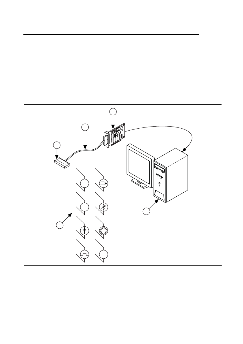
Figure 1-1 shows a typical DAQ system setup, which includes transducers, signal conditioning,
cables that connect the various devices to the accessories, the analog output device, and the
programming software. Refer to the Using Accessories with Devices section for a list of devices
and their compatible accessories.
Figure 1-1. DAQ System Setup
4
3
2
+
V
–
+
HV
–
5
1
1 Sensors and Transducers
2 Terminal Block Accessory
3 Cable Assembly
mV
+
–
4DAQ Device
5 Personal Computer
© National Instruments | 1-1
+
–
Page 11
Chapter 1 DAQ System Overview
Safety Guidelines
Operate the device only as described in this document.
Caution This icon denotes a caution, which advises you of precautions to take to
avoid injury, data loss, or a system crash.
Caution The protection provided by the device can be impaired if it is used in a
manner not described in this document. Misuse of the device can result in a hazard.
You can compromise the safety protection built into the device if the device is
damaged in any way. If the device is damaged, contact National Instruments for
repair.
Caution Do not substitute parts or modify the device except as described in this
document. Use the device only with the chassis, modules, accessories, and cables
specified in the installation instructions.
Caution You must have all covers and filler panels installed during operation of the
device. Do not operate the device without verifying that the cover is correctly
attached and the device is completely closed.
Electromagnetic Compatibility Guidelines
This product was tested and complies with the regulatory requirements and limits for
electromagnetic compatibility (EMC) stated in the product specifications. These requirements
and limits provide reasonable protection against harmful interference when the product is
operated in the intended operational electromagnetic environment.
This product is intended for use in industrial locations. However, harmful interference may
occur in some installations, when the product is connected to a peripheral device or test object,
or if the product is used in residential or commercial areas. To minimize interference with radio
and television reception and prevent unacceptable performance degradation, install and use this
product in strict accordance with the instructions in the product documentation.
Furthermore, any modifications to the product not expressly approved by National Instruments
could void your authority to operate it under your local regulatory rules.
Caution To ensure the specified EMC performance, operate this product only with
shielded cables and accessories. Do not use unshielded cables or accessories unless
they are installed in a shielded enclosure with properly designed and shielded
input/output ports and connected to the product using a shielded cable. If unshielded
cables or accessories are not properly installed and shielded, the EMC specifications
for the product are no longer guaranteed.
1-2 | ni.com
Page 12
Analog Output Series User Manual
Analog Output
Digital I/O
Counters
PFI
Digital
Routing
RTSI
Bus
Interface
Bus
I/O Connector
Caution To ensure the specified EMC performance of the DAQCard-6715, the
length of the I/O cable must be no longer than 3 m (10 ft). For all other products, the
length of the I/O cable must be no longer than 30 m (100 ft).
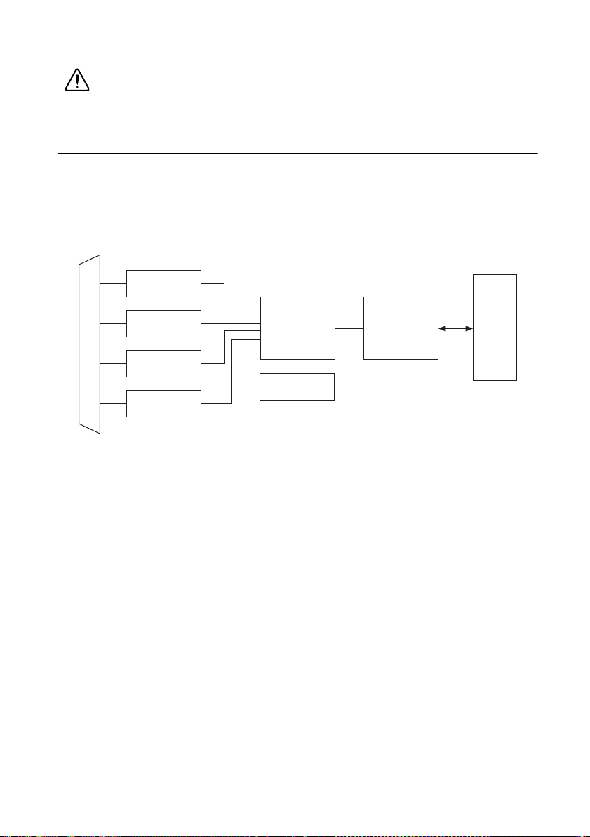
DAQ Hardware
DAQ hardware digitizes signals, performs D/A conversions to generate analog output signals,
and measures and controls digital I/O signals. Figure 1-2 shows the components common to all
AO Series devices. The following sections contain more information about specific components
of the DAQ hardware.
Figure 1-2. Analog Output Block Diagram
DAQ-STC
Analog output devices use the National Instruments DAQ system timing controller (DAQ-STC)
for time-related functions. The DAQ-STC consists of the following three timing groups:
• AI—two 24-bit, two 16-bit counters (not used on AO Series devices)
• AO—three 24-bit, one 16-bit counter
• General-purpose counter/timer functions—two 24-bit counters
You can independently configure the groups for timing resolutions of 50 ns or 10 µs. With the
DAQ-STC, you can interconnect a wide variety of internal timing signals to other internal
blocks. The interconnection scheme is flexible and completely software-configurable.
The DAQ-STC offers PFI lines to import external timing and trigger signals or to export
internally generated clocks and triggers. The DAQ-STC also supports buffered operations, such
as buffered waveform acquisition, buffered waveform generation, and buffered period
measurement. It also supports numerous non-buffered operations, such as single pulse or pulse
train generation, digital input, and digital output.
© National Instruments | 1-3
Page 13

Chapter 1 DAQ System Overview
Calibration Circuitry
Calibration is the process of making adjustments to a measurement device to reduce errors
associated with measurements. Without calibration, the measurement results of your device will
drift over time and temperature. Calibration adjusts for these changes to improve measurement
accuracy and ensure that your product meets its required specifications.
DAQ devices have high precision analog circuits that must be adjusted to obtain optimum
accuracy in your measurements. Calibration determines what adjustments these analog circuits
should make to the device measurements. During calibration, the value of a known, high
precision measurement source is compared to the value your device acquires or generates. The
adjustment values needed to minimize the difference between the known and measured values
are stored in the EEPROM of the device as calibration constants. Before performing a
measurement, these constants are read out of the EEPROM and are used to adjust the calibration
hardware on the device. NI-DAQ determines when this is necessary and does it automatically.
If you are not using NI-DAQ, you must load these values yourself.
You can calibrate AO Series devices in the following two ways.
Internal or Self-Calibration
Self-calibration is a process to adjust the device relative to a highly accurate and stable internal
reference on the device. Self-calibration is similar to the autocalibration or autozero found on
some instruments. You should perform a self-calibration whenever environmental conditions,
such as ambient temperature, change significantly. To perform self-calibration, use the
self-calibrate function or VI that is included with your driver software. Self-calibration requires
no external connections.
External Calibration
External calibration is a process to adjust the device relative to a traceable, high precision
calibration standard. The accuracy specifications of your device change depending on how long
it has been since your last external calibration. National Instruments recommends that you
calibrate your device at least as often as the intervals listed in the accuracy specifications.
For a detailed calibration procedure for AO Series devices, refer to the AO Waveform
Calibration Procedure for NI-DAQmx document by selecting Manual Calibration Procedures
ni.com/calibration.
at
Cables and Accessories
NI offers a variety of products to use with Analog Output Series devices, including:
• BNC accessories
• Connector blocks with screw terminals
• I/O connector cables
1-4 | ni.com
Page 14

Analog Output Series User Manual
• RTSI bus cables
• Low channel-count digital signal conditioning modules, devices, and accessories
For more specific information about these products, refer to ni.com.
The following sections contain information on how to select accessories for your AO Series
device.
Using Accessories with Devices
Go to ni.com/info and enter the Info Code AOcables for the most current list of supported
cables and accessories for the following analog output devices.
Table 1-1. Accessories and Cables for Analog Output Devices
Accessories
Device
Cables Terminal Blocks
NI 6711/6713 SH68-68-EPM
(Recommended, Shielded)
R6868 (Low Cost)
NI DAQCard-6715 SHC68-68-EPM
(Recommended, Shielded)
SHC68U-68-EP (Shielded)
RC68-68 (Unshielded)
NI 6722 SH68-C68-S
(Recommended, Shielded)
RC68-68 (Low Cost)
BNC-2110
CA1000
CB-68LP
CB-68LPR
SCB-68
SCB-68A
TBX-68
TB-2705 (PXI only)
BNC-2110
CA1000
CB-68LP
CB-68LPR
SCB-68A
SCB-68
TBX-68
BNC-2110
CA1000
CB-68LP
CB-68LPR
SCB-68A
SCB-68
TBX-68
© National Instruments | 1-5
Page 15
Chapter 1 DAQ System Overview
Table 1-1. Accessories and Cables for Analog Output Devices (Continued)
Accessories
Device
NI 6723
(AO 0–7 & DIGITAL connector)
SH68-C68-S
(Recommended, Shielded)
Cables Terminal Blocks
RC68-68
(Low Cost)
NI 6723 (AO 8–31 connector) SH68-C68-S
(Recommended, Shielded)
RC68-68
(Low Cost)
NI 6731/6733 SH68-68-EPM
(Recommended)
R6868
(Low Cost)
BNC-2110
CA1000
CB-68LP
CB-68LPR
SCB-68A
SBC-68
TBX-68
BNC-2115
CA-1000
CB-68LP
CB-68LPR
SCB-68A
SCB-68
TBX-68
BNC-2110
CA1000
CB-68LP
CB-68LPR
SCB-68
SCB-68A
TBX-68
TB-2705 (PXI only)
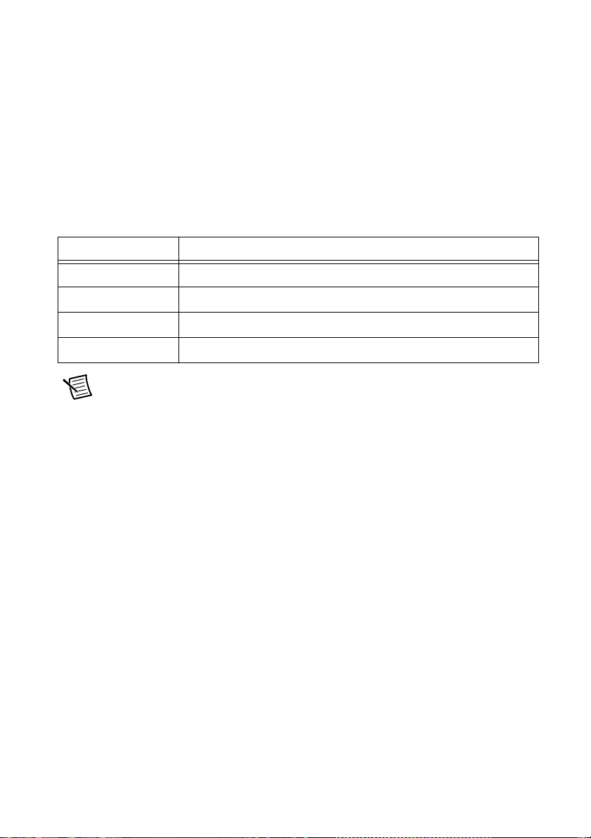
Table 1-2. Overview of DAQ Accessories for Analog Output Devices
Accessory Description
BNC-2110 BNC connector block for 68-pin analog output devices
BNC-2115 BNC connector block for extended I/O
CA-1000 Per-channel custom connectivity connector accessory enclosure
CB-68LP, CB-68LPR 68-pin, low-cost screw terminal block
SCB-68A, SCB-68 68-pin, shielded screw terminal block with breadboard areas.
The SCB-68A is a newer design recommended for all new
applications over the SCB-68.
TBX-68 68-pin, DIN rail-mountable screw terminal block
1-6 | ni.com
Page 16
Analog Output Series User Manual
Custom Cabling
Follow these guidelines if you want to develop your own cable.
• Route the analog lines separately from the digital lines.
• When using a cable shield, use separate shields for the analog and digital halves of the
cable. Failure to do so results in noise coupling into the analog signals from transient digital
signals.
Table 1-3 shows the recommended connectors to use with the I/O connector on your AO device.
Table 1-3. Recommended AO Connectors
Device Connector
NI 6711/6713 Honda 68-position, solder cup, female connector Honda backshell
NI DAQCard-6715 AMP 68-position, VHDCI AMP backshell
NI 6722/6723 AMP 68-position, VHDCI AMP backshell
NI 6731/6733 Honda 68-position, solder cup, female connector Honda backshell
Note When the NI DAQCard-6715 is in the upper PCMCIA slot, you can maintain
access to the adjacent slot by using an inverted VHDCI connector.
For more information on the connectors used for DAQ devices, refer to the KnowledgeBase
document, Specifications and Manufacturers for Board Mating Connectors. To access this
document, go to ni.com/info and enter the info code rdsmbm.
Field Wiring Considerations
The following recommendations apply for all signal connections to the AO Series device.
• Separate the signal lines of the AO Series device from high-current or high-voltage lines.
These lines can induce currents in or voltages on the signal lines of the AO Series device if
they run in close parallel paths. To reduce the magnetic coupling between lines, separate
them by a reasonable distance if they run in parallel, or run the lines at right angles to each
other.
•Do not run signal lines through conduits that also contain power lines.
• Protect signal lines from magnetic fields caused by electric motors, welding equipment,
breakers, or transformers by running them through special metal conduits.
Refer to the NI Developer Zone document, Field Wiring and Noise Considerations for Analog
Signals, for more information. To access this document, go to
Code rdfwin.
ni.com/info and enter the Info
© National Instruments | 1-7
Page 17

Chapter 1 DAQ System Overview
Programming Devices in Software
National Instruments measurement devices are packaged with NI-DAQmx driver software, an
extensive library of functions and VIs you can call from your application software, such as
LabVIEW or LabWindows/CVI, to program all the features of your NI measurement devices.
Driver software has an application programming interface (API), which is a library of VIs,
functions, classes, attributes, and properties for creating applications for your device.
NI-DAQmx includes a collection of programming examples to help you get started developing
an application. You can modify example code and save it in an application. You can use
examples to develop a new application or add example code to an existing application.
To locate LabVIEW and LabWindows/CVI examples, open the National Instruments Example
Finder:
• In LabVIEW, select Help»Find Examples.
• In LabWindows/CVI, select Help»NI Example Finder.
Measurement Studio, Visual Basic, and ANSI C examples are in the following directories:
• NI-DAQmx examples for Measurement Studio-supported languages are in the following
directories:
– NI-DAQ\Examples\MStudioVCxxxx
• Traditional NI-DAQ (Legacy) examples for Visual Basic are in the following two
directories:
– NI-DAQ\Examples\DotNETx.x
• NI-DAQmx examples for ANSI C are in the NI-DAQ\Examples\DAQmx ANSI C
directory
For additional examples, refer to ni.com/examples.
1-8 | ni.com
Page 18

I/O Connector
This chapter contains information about the AO Series I/O connectors.
Note Some hardware accessories may not yet reflect the NI-DAQmx terminal
names. If you are using an AO Series device in Traditional NI-DAQ (Legacy), refer
to Table 2-1 for the Traditional NI-DAQ (Legacy) signal names.
68-Pin AO I/O Connector Pinouts
Figure 2-1, Figure 2-2, and Figure 2-3 show the pinouts of 68-pin AO Series devices.
2
© National Instruments | 2-1
Page 19
Chapter 2 I/O Connector
FREQ OUT
CTR 0 OUT
PFI 9/CTR 0 GATE
D GND
PFI 6/AO START TRIG
PFI 5/AO SAMP CLK
D GND
+5 V
D GND
PFI 1
PFI 0
D GND
D GND
+5 V
D GND
P0.6
P0.1
D GND
P0.4
AO EXT REF
AO 1
AO 0
AO GND
AO GND
AO 3
AO GND
AO GND
NC
AO GND
NC
AO GND
AO GND
NC
AO GND
D GND
PFI 8/CTR 0 SOURCE
PFI 7
CTR 1 OUT
PFI 4/CTR 1 GATE
PFI 3/CTR 1 SOURCE
PFI 2
D GND
D GND
D GND
EXT STROBE
NC
P0.3
P0.7
P0.2
D GND
P0.5
P0.0
D GND
AO GND
AO GND
AO GND
AO 2
AO GND
AO GND
NC
AO GND
NC
AO GND
AO GND
NC
AO GND
AO GND
NC
1 35
2 36
337
4 38
5 39
640
741
8 42
943
10 44
11 45
12 46
13 47
14 48
15 49
16 50
17 51
18 52
19 53
20 54
21 55
22 56
23 57
24 58
25 59
26 60
27 61
28 62
29 63
3
064
316
5
3266
33 67
3
468
NC = No Connect
2-2 | ni.com
Figure 2-1. NI 6711/6731 68-Pin AO I/O Connector Pinout
Page 20
Figure 2-2. NI 6713/DAQCard-6715/NI 6733 68-Pin AO I/O Connector Pinout
FREQ OUT
CTR 0 OUT
PFI 9/CTR 0 GATE
D GND
PFI 6/AO START TRIG
PFI 5/AO SAMP CLK
D GND
+5 V
D GND
PFI 1
PFI 0
D GND
D GND
+5 V
D GND
P0.6
P0.1
D GND
P0.4
AO EXT REF
AO 1
AO 0
AO GND
AO GND
AO 3
AO GND
AO GND
AO 5
AO GND
AO 6
AO GND
AO GND
NC
AO GND
D GND
PFI 8/CTR 0 SOURCE
PFI 7
CTR 1 OUT
PFI 4/CTR 1 GATE
PFI 3/CTR 1 SOURCE
PFI 2
D GND
D GND
D GND
EXT STROBE
NC
P0.3
P0.7
P0.2
D GND
P0.5
P0.0
D GND
AO GND
AO GND
AO GND
AO 2
AO GND
AO GND
AO 4
AO GND
NC
AO GND
AO GND
AO 7
AO GND
AO GND
NC
1 35
2 36
337
4 38
5 39
640
741
8 42
943
10 44
11 45
12 46
13 47
14 48
15 49
16 50
17 51
18 52
19 53
20 54
21 55
22 56
23 57
24 58
25 59
26 60
27 61
28 62
29 63
3
064
316
5
3266
33 67
3
468
NC = No Connect
TitleShort-Hidden (cross reference text)
© National Instruments | 2-3
Page 21
Chapter 2 I/O Connector
Figure 2-3. NI 6722 68-Pin AO I/O Connector Pinout
NC
AO GND
AO GND
AO 7
AO GND
AO GND
NC
AO GND
AO 4
AO GND
AO GND
AO 2
AO GND
AO GND
AO GND
D GND
P0.0
P0.5
D GND
P0.2
P0.7
P0.3
NC
EXT STROBE
D GND
PFI 2
PFI 3/CTR 1 SOURCE
PFI 4/CTR 1 GATE
CTR 1 OUT
D GND
PFI 7
PFI 8/CTR 0 SOURCE
D GND
D GND
3468
AO GND
3367
NC
3266
AO GND
3165
AO GND
3064
AO 6
2963
AO GND
2862
AO 5
2761
AO GND
2660
AO GND
2559
AO 3
2458
AO GND
2357
AO GND
2256
55
54
53
52
51
50
49
48
47
46
45
44
43
42
41
40
39
38
37
36
35
AO 0
21
AO 1
20
CAL
19
P0.4
18
D GND
17
P0.1
16
P0.6
15
D GND
14
+5 V
13
D GND
12
D GND
11
PFI 0
10
PFI 1
9
D GND
8
+5 V
7
D GND
6
PFI 5/AO SAMP CLK
5
PFI 6/AO START TRIG
4
D GND
PFI 9/CTR 0 GATE
3
CTR 0 OUT
2
FREQ OUT
1
TERMINAL 34TERMINAL 68
TERMINAL 1TERMINAL 35
NC = No Connect
For a detailed description of each signal, refer to I/O Connector Signal Descriptions.
2-4 | ni.com
Page 22

TitleShort-Hidden (cross reference text)
68-68-Pin Extended AO I/O Connector Pinout
The NI 6723 has two 68-pin I/O connectors. Figure 2-4 shows the pin assignments for both
connectors on the NI 6723.
Figure 2-4. NI 6723 68-68-Pin Extended AO I/O Connector Pinout
AO 0–7 & DIGITAL Connector
AO 8–31 Connector
AO GND
AO GND
AO 7
AO GND
AO GND
AO GND
AO 4
AO GND
AO GND
AO 2
AO GND
AO GND
AO GND
D GND
P0.0
P0.5
D GND
P0.2
P0.7
P0.3
EXT STROBE
D GND
PFI 3/CTR 1 SOURCE
PFI 8/CTR 0 SOURCE
PFI 2
PFI 4/CTR 1 GATE
CTR 1 OUT
D GND
PFI 7
D GND
D GND
3468
NC
NC
NC
AO GND
3367
NC
3266
AO GND
3165
AO GND
3064
AO 6
2963
AO GND
2862
AO 5
2761
AO GND
2660
AO GND
2559
AO 3
2458
AO GND
2357
AO GND
2256
AO 0
2155
AO 1
2054
CAL
1953
P0.4
1852
D GND
1751
P0.1
1650
P0.6
1549
D GND
1448
+5 V
1347
D GND
1246
D GND
1145
PFI 0
1044
PFI 1
943
D GND
842
+5 V
741
D GND
640
PFI 5/AO SAMP CLK
539
PFI 6/AO START TRIG
438
D GND
337
PFI 9/CTR 0 GATE
236
CTR 0 OUT
FREQ OUT
135
AO 8
AO GND
AO GND
AO 11
AO GND
AO GND
AO 14
AO GND
AO GND
AO 17
AO GND
AO GND
AO 20
AO GND
AO GND
AO 23
AO GND
AO GND
AO 26
AO GND
AO GND
AO 29
AO GND
AO GND
3468
AO GND
AO 9
3367
3266
AO 10
3165
AO GND
3064
AO 12
AO 13
2963
AO GND
2862
AO 15
2761
AO 16
2660
AO GND
2559
AO 18
2458
AO 19
2357
2256
NC
NC
NC
NC
NC
NC
NC
NC
NC
NC
NC
2155
AO GND
AO 21
2054
1953
AO 22
1852
AO GND
1751
AO 24
1650
AO 25
AO GND
1549
1448
AO 27
AO 28
1347
AO GND
1246
AO 30
1145
AO 31
1044
NC
943
NC
842
NC
741
NC
640
NC
539
NC
438
NC
337
NC
236
NC
135
TERMINAL 68
TERMINAL 35
TERMINAL 34
TERMINAL 1
NC = No Connect
For a detailed description of each signal, refer to I/O Connector Signal Descriptions.
Terminal Name Equivalents
With NI-DAQmx, National Instruments has revised its terminal names so they are easier to
understand and more consistent among National Instruments hardware and software products.
The revised terminal names used in this document are usually similar to the names they replace.
Refer to Table 2-1 for a list of Traditional NI-DAQ (Legacy) terminal names and their
NI-DAQmx equivalents.
© National Instruments | 2-5
Page 23
Chapter 2 I/O Connector
Table 2-1. Terminal Name Equivalents.
Traditional NI-DAQ (Legacy) NI-DAQmx
ACH# AI #
ACH# + AI # +
ACH# - AI # -
ACHGND AI GND
AIGND AI GND
AISENSE AI SENSE
AISENSE2 AI SENSE 2
AOGND AO GND
CONVERT* AI CONV CLK or AI CONV
DAC0OUT AO 0
DAC1OUT AO 1
DGND D GND
DIO_# P0.#
DIO# P0.#
DIOA#, DIOB#, DIOC#... P0.#, P1.#, P2.#...
EXTREF AO EXT REF or EXT REF
EXT_STROBE EXT STROBE
FREQ_OUT FREQ OUT or F OUT
GPCTR0_GATE CTR 0 GATE
GPCTR0_OUT CTR 0 OUT
GPCTR0_SOURCE CTR 0 SOURCE or CTR 0 SRC
GPCTR1_GATE CTR 1 GATE
GPCTR1_OUT CTR 1 OUT
GPCTR1_SOURCE CTR 1 SOURCE or CTR 1 SRC
PA#, PB#, PC#... P0.#, P1.#, P2.#...
2-6 | ni.com
Page 24
TitleShort-Hidden (cross reference text)
Table 2-1. Terminal Name Equivalents. (Continued)
Traditional NI-DAQ (Legacy) NI-DAQmx
PFI# PFI #
PFI_# PFI #
SCANCLK AI HOLD COMP or AI HOLD
SISOURCE AI Sample Clock Timebase
STARTSCAN AI SAMP CLK or AI SAMP
TRIG1 AI START TRIG or AI START
TRIG2 AI REF TRIG or REF TRIG
UISOURCE AO Sample Clock Timebase
UPDATE AO SAMP CLK or AO SAMP
WFTRIG AO START TRIG or AO START
I/O Connector Signal Descriptions
Table 2-2 describes the signals found on the I/O connectors.
Table 2-2. I/O Connector Signal Descriptions
I/O Connector
Pin
Reference Direction Signal Description
AO GND — — Analog Output Ground—The AO
voltages and the external reference voltage
are referenced to these pins.
AO <0..31> AO GND Output Analog Output channels 0 through
31—These pins supply the voltage outputs
of their respective channels.
D GND — — Digital Ground—These pins supply the
reference for the digital signals at the I/O
connector as well as the +5 VDC supply.
P0.<0..7> D GND Input or
Output
Digital I/O signals—These pins drive and
receive digital signals. P0.6 and P0.7 can
control the up/down signal of Counters 0
and 1, respectively.
© National Instruments | 2-7
Page 25

Chapter 2 I/O Connector
Table 2-2. I/O Connector Signal Descriptions (Continued)
I/O Connector
Pin
Reference Direction Signal Description
+5 V D GND Output +5 VDC source—These pins provide
+5 V power.
AO EXT REF D GND Input External Reference—This pin is the
external reference input for the AO
circuitry.
AI HOLD COMP D GND Output AI Hold Complete—This pin is used to
control some NI accessories.
EXT STROBE D GND Output External Strobe—This pin is used to
control some NI accessories.
PFI 0 D GND Input PFI 0—As an input for digital signals, this
pin is a general-purpose input terminal.
For an explanation of PFI signals, refer to
the Connecting Timing Signals section.
PFI 1 D GND Input PFI 1—As an input, this is a
general-purpose input terminal.
PFI 2 D GND Input PFI 2—As an input, this pin is a
general-purpose input terminal.
PFI 3/CTR 1
SOURCE
PFI 4/CTR 1
GATE
2-8 | ni.com
D GND Input PFI 3—As an input, this pin is a
general-purpose input terminal. This is the
default input for the Ctr1Source signal.
Output Counter 1 Source Signal—As an output,
this pin emits the selected Ctr1Source
signal. This signal reflects the actual
source signal connected to Counter 1. For
more information, refer to Chapter 5,
Counters.
D GND Input PFI 4—As an input, this pin is a
general-purpose input terminal. This is the
default input for the Ctr1Gate signal.
Output Counter 1 Gate Signal—As an output,
this pin emits the selected Ctr1Gate signal.
This signal reflects the actual gate signal
connected to Counter 1. For more
information, refer to Chapter 5, Counters.
Page 26

TitleShort-Hidden (cross reference text)
Table 2-2. I/O Connector Signal Descriptions (Continued)
I/O Connector
Pin
Reference Direction Signal Description
CTR 1 OUT D GND Output Counter 1 Output Signal—This pin
emits the Ctr1InternalOutput signal. For
more information, refer to Chapter 5,
Counters.
PFI 5/AO
SAMP CLK
D GND Input PFI 5—As an input, this pin is a
general-purpose input terminal.
Output AO Sample Clock Signal—As an output,
this pin emits the ao/SampleClock signal.
A high-to-low transition of this signal
indicates a new sample is being generated.
For more information, refer to Chapter 3,
Analog Output.
PFI 6/AO START
TRIG
D GND Input PFI 6—As an input, this pin is a
general-purpose input terminal. This is the
default input for the ao/StartTrigger signal.
Output AO Start Trigger Signal—As an output,
this pin emits the ao/StartTrigger signal. A
low-to-high transition of this signal
indicates the start of a generation. For
more information, refer to Chapter 3,
Analog Output.
PFI 7 D GND Input PFI 7—As an input, this pin is a
general-purpose input terminal.
PFI 8/CTR 0
SOURCE
D GND Input PFI 8—As an input, this pin is a
general-purpose input terminal and can
also be used to route signals directly to the
RTSI bus. This is the default input for the
Ctr0Source signal.
Output Counter 0 Source Signal—As an output,
this pin emits the Ctr0Source signal. This
signal reflects the actual source signal
connected to Counter 0. For more
information, refer to Chapter 5, Counters.
© National Instruments | 2-9
Page 27
Chapter 2 I/O Connector
Table 2-2. I/O Connector Signal Descriptions (Continued)
I/O Connector
Pin
Reference Direction Signal Description
PFI 9/CTR 0
GATE
D GND Input PFI 9—As an input, this pin is a
general-purpose input terminal and can
also be used to route signals directly to the
RTSI bus. This is the default input for the
Ctr0Gate signal.
Output Counter 0 Gate Signal—As an output,
this pin emits the Ctr0Gate signal. This
signal reflects the actual gate signal
connected to Counter 0. For more
information, refer to Chapter 5, Counters.
CTR 0 OUT D GND Input Counter 0 Output Signal—As an input,
this pin can be used to route signals
directly to the RTSI bus. For more
information, refer to Chapter 5, Counters.
Output As an output, this pin emits the
Ctr0InternalOutput signal.
CAL D GND Input Calibration—Voltage input for external
calibration. For more information on using
this signal, refer to the AO Waveform
Calibration Procedure for NI-DAQmx
document by selecting Manual
Calibration Procedures at
calibration
.
ni.com/
FREQ OUT D GND Output Frequency Output Signal—This output
is from the frequency generator. For more
information, refer to Chapter 5, Counters.
Caution Connections that exceed any of the maximum ratings of input or output
signals on the AO Series device can damage the device and the computer. Refer to
the specifications document for your device for more information on maximum input
ratings for each signal. NI is not liable for any damage resulting from signal
connections that exceed the maximum ratings.
+5 V Power Source
The +5 V pins on the I/O connector supply +5 V power. You can use these pins, referenced to
D GND, to power external circuitry. A self-resetting fuse protects the supply from overcurrent
2-10 | ni.com
Page 28

TitleShort-Hidden (cross reference text)
conditions. The fuse resets automatically within a few seconds after the overcurrent condition is
removed.
Power rating: +4.65 to +5.25 VDC at 1 A (0.75 A for the DAQCard-6715)
The +5 V line on the connector of the DAQCard-6715 is fused at 0.75 A. However, the actual
current available can be limited below this value by the host computer. NI recommends limiting
current from this line to 250 mA.
Caution Never connect these +5 V power pins to analog or digital ground or to any
other voltage source on the AO Series device or any other device. Doing so can
damage the device and the computer. NI is not liable for damage resulting from such
a connection.
© National Instruments | 2-11
Page 29

Analog Output
AO 0
AO 1
DAC0
DAC1
AO FIFO
AO Data
AO Sample Clock
Polarity Select
Reference Select
Figure 3-1 shows the analog output circuitry of AO Series devices.
Figure 3-1. Analog Output Circuitry Block Diagram
Analog Output Fundamentals
Analog Output Circuitry
DACs
Digital-to-analog converters (DACs) convert digital codes to analog voltages.
3
DAC FIFO
The DAC FIFO enables analog output waveform generation. It is a first-in-first-out (FIFO)
memory buffer between the computer and the DACs that allows you to download all the points
of a waveform to your board without host computer interaction.
AO Sample Clock
The DAC reads a sample from the FIFO with every cycle of the AO Sample Clock signal and
generates the AO voltage. For more information on the AO Sample Clock signal, refer to the
Waveform Generation Timing Signals section.
Reference Selection
(NI 6711/6713/DAQCard-6715 and NI 6731/6733 Only) Reference selection allows you to set
the AO range. Refer to Table 3-1 to set the range for your device.
© National Instruments | 3-1
Page 30

Chapter 3 Analog Output
20 V
65,536
---------------- 305 μV=
Table 3-1. AO Reference Selection Options
AO Range Polarity Reference Select
±10 V Bipolar Internal
±EXT REF Bipolar AO External Reference Signal
Analog Output Resolution
You can calculate the least significant bit (LSB), or the minimal allowed voltage change, on a
voltage output on your AO Series device as follows:
LSB = output voltage range/2
where the output range is determined by your reference selection. Using AO EXT REF, you can
reduce the output voltage range and lower the LSB, the minimum allowed voltage change. For
more information on using the AO External Reference signal, refer to the Reference Selection
(NI 6711/6713/DAQCard-6715 and NI 6731/6733 Only) section.
The following equation is an example of this formula using the NI 6731/6733.
The denominator in the equation is derived from 2
use 16-bit DACs.
resolution of your device
16
= 65,536, since the NI 6731/6733 devices
Reference Selection (NI 6711/6713/DAQCard-6715 and NI 6731/6733 Only)
You can connect each DAC to the device internal reference of 10 V or to the external reference
signal connected to the external reference (AO EXT REF) pin on the I/O connector. This signal
applied to AO EXT REF should be within ±11 V of AO GND. You do not need to configure all
channels for the same mode. Using AO EXT REF to reduce the output voltage range results in
a higher resolution at the adjusted range.
Reglitch Selection (NI 6711/6713 Only)
In normal operation, a DAC output glitches whenever it is updated with a new value. The glitch
energy differs from code to code and appears as distortion in the frequency spectrum. Each AO
channel contains a reglitch circuit that generates uniform glitch energy at every code rather than
large glitches at the major code transitions. This uniform glitch energy appears as a multiple of
the update rate in the frequency spectrum. This reglitch circuit does not eliminate the glitches; it
only makes them more uniform in size. By default, reglitching is disabled for all channels;
however, you can use NI-DAQ to independently enable reglitching for each channel.
3-2 | ni.com
Page 31

TitleShort-Hidden (cross reference text)
Minimizing Glitches on the Output Signal
When you use a DAC to generate a waveform, you may observe glitches on the output signal.
These glitches are normal; when a DAC switches from one voltage to another, it produces
glitches due to released charges. The largest glitches occur when the most significant bit (MSB)
of the DAC code switches. You can build a lowpass deglitching filter to remove some of these
glitches, depending on the frequency and nature of the output signal. Visit
for more information on minimizing glitches.
ni.com/support
AO Data Generation Methods
When performing an analog output operation, there are several different data generation
methods available. You can either perform software-timed or hardware-timed generations.
Hardware-timed generations can be non-buffered or buffered.
Software-Timed Generations
With a software-timed generation, software controls the rate at which data is generated. Software
sends a separate command to the hardware to initiate each DAC conversion. In NI-DAQmx,
software-timed generations are referred to as On Demand timing. Software-timed generations
are also referred to as immediate or static operations. They are typically used for writing a single
value out, such as a constant DC voltage.
Hardware-Timed Generations
With a hardware-timed generation, a digital hardware signal controls the rate of the generation.
This signal can be generated internally on your device or provided externally.
Hardware-timed generations have several advantages over software-timed generations:
• The time between samples can be much shorter.
• The timing between samples can be deterministic.
• Hardware-timed generations can use hardware triggering. For more information, refer to
Chapter 10, Triggering.
Hardware-timed operations can be buffered or non-buffered. A buffer is a temporary storage in
computer memory for acquired or to-be-generated samples.
Buffered
In a buffered generation, data is moved from a PC buffer to the DAQ device’s onboard FIFO
using DMA or interrupts before it is written to the DACs one sample at a time. Buffered
generations typically allow for much faster transfer rates than non-buffered generations because
data is moved in large blocks, rather than one point at a time. For more information on DMA and
interrupt requests, refer to the Data Transfer Methods section of Chapter 9, Bus Interface.
One property of buffered I/O operations is the sample mode. The sample mode can be either
finite or continuous.
© National Instruments | 3-3
Page 32

Chapter 3 Analog Output
Finite sample mode generation refers to the generation of a specific, predetermined number of
data samples. After the specified number of samples has been written out, the generation stops.
Continuous generation refers to the generation of an unspecified number of samples. Instead of
generating a set number of data samples and stopping, a continuous generation continues until
you stop the operation. There are several different methods of continuous generation that control
what data is written. These methods are regeneration, FIFO regeneration and non-regeneration
modes.
Regeneration is the repetition of the data that is already in the buffer. Standard regeneration is
when data from the PC buffer is continually downloaded to the FIFO to be written out. New data
can be written to the PC buffer at any time without disrupting the output.
With FIFO regeneration, the entire buffer is downloaded to the FIFO and regenerated from there.
After the data is downloaded, new data cannot be written to the FIFO. To use FIFO regeneration,
the entire buffer must fit within the FIFO size. The advantage of using FIFO regeneration is that
it does not require communication with the main host memory when the operation is started,
thereby preventing any problems that may occur due to excessive bus traffic.
With non-regeneration, old data will not be repeated. New data must be continually written to
the buffer. If the program does not write new data to the buffer at a fast enough rate to keep up
with the generation, the buffer will underflow and cause an error.
Non-Buffered
In hardware-timed non-buffered generations, data is written directly to the FIFO on the device.
Typically, hardware-timed non-buffered operations are used to write single samples with known
time increments between them and good latency.
Analog Output Triggering
Analog output supports two different triggering actions: start and pause. A digital hardware
trigger can initiate these actions. All AO Series devices support digital triggering.
The AO Start Trigger Signal section and AO Pause Trigger Signal section contain information
about the analog output trigger signals.
Refer to Chapter 10, Triggering, for more information about triggers.
3-4 | ni.com
Page 33

TitleShort-Hidden (cross reference text)
Load
Load
V OUT
V OUT
+
–
+
–
AO GND
AO 1
Analog Output Channels
AO Series Device
AO 0
Channel 1
Channel 0
I/O Connector
V
ref
External
Reference
Signal
(Optional)
AO EXT REF
RTSI 7
20 MHz
Timebase
÷200
Master
Timebase
Onboard
Clock
PFI 0–9,
RTSI 0–6
ao/SampleClock
Timebase
Onboard
Clock
Divisor
ao/SampleClock
Ctr1InternalOutput
PFI 0–9,
RTSI 0–6
÷
Connecting Analog Output Signals
Figure 3-2 shows how to connect loads to AO 0 and AO 1.
Figure 3-2. Analog Output Connections for AO 0 and AO 1
Note AO EXT REF is not available on the NI 6722/6723.
Waveform Generation Timing Signals
Waveform Generation Timing Summary
There is one AO Sample Clock that causes all AO channels to update simultaneously. Figure 3-3
summarizes the timing and routing options provided by the analog output timing engine.
Figure 3-3. Analog Output Engine Routing Options
AO Start Trigger Signal
You can use the AO Start Trigger (ao/StartTrigger) signal to initiate a waveform generation. If
you do not use triggers, you begin a generation with a software command.
© National Instruments | 3-5
Page 34

Chapter 3 Analog Output
Rising-Edge
Polarity
Falling-Edge
Polarity
t
w
tw = 10 ns minimum
Using a Digital Source
To use ao/StartTrigger, specify a source and an edge. The source can be an external signal
connected to any PFI or RTSI <0..6> pin. The source can also be one of several internal signal
on your DAQ device. Refer to Device Routing in MAX in the NI-DAQmx Help or the
LabVIEW Help for more information.
Figure 3-4 shows the timing requirements of the ao/StartTrigger digital source.
Figure 3-4. ao/StartTrigger Timing Requirements
Outputting the AO Start Trigger Signal
You can configure the PFI 6/AO START TRIG pin to output the ao/StartTrigger signal. The
output pin reflects the ao/StartTrigger signal regardless of what signal you specify as its source.
The output is an active high pulse. Figure 3-5 shows the timing behavior of the PFI 6/AO START
TRIG pin when the pin is an output.
Figure 3-5. PFI 6/AO START TRIG Timing Behavior
t
w
tw = 50 –100 ns
The PFI 6/AO START TRIG pin is configured as an input by default.
AO Pause Trigger Signal
You can use the AO Pause trigger signal (ao/PauseTrigger) to mask off samples in a DAQ
sequence. That is, when ao/PauseTrigger is active, no samples occur.
The ao/PauseTrigger does not stop a sample that is in progress. The pause does not take effect
until the beginning of the next sample. This signal is not available as an output.
3-6 | ni.com
Page 35

TitleShort-Hidden (cross reference text)
Using a Digital Source
To use ao/Pause Trigger, specify a source and a polarity. The source can be an external signal
connected to any PFI or RTSI <0..6> pin. The source can also be one of several other internal
signals on your DAQ device. Refer to Device Routing in MAX in the NI-DAQmx Help or the
LabVIEW Help for more information.
Also, specify whether the samples are paused when ao/PauseTrigger is at a logic high or low
level.
AO Sample Clock Signal
You can use the AO Sample Clock (ao/SampleClock) signal to initiate AO samples. Each
sample updates the outputs of all of the DACs.
The source of the ao/SampleClock signal can be internal or external. You can specify whether
the DAC update begins on the rising edge or falling edge of the ao/SampleClock signal.
Using an Internal Source
By default, ao/SampleClock is created internally by dividing down the
ao/SampleClockTimebase. For more information, refer to the AO Sample Clock Timebase
Signal section.
Several other internal signals can be routed to the sample clock. Refer to Device Routing in MAX
in the NI-DAQmx Help or the LabVIEW Help for more information.
Using an External Source
You can use a signal connected to any PFI or RTSI <0..6> pin as the source of ao/SampleClock.
Figure 3-6 shows the timing requirements of the ao/SampleClock source.
Figure 3-6. ao/SampleClock Timing Requirements
t
w
Rising-Edge
Polarity
Falling-Edge
Polarity
t
= 10 ns minimum
w
© National Instruments | 3-7
Page 36

Chapter 3 Analog Output
t
w
= 50–75 ns
t
w
Outputting the AO Sample Clock Signal
You can configure the PFI 5/AO SAMP CLK pin to output the ao/SampleClock signal. The
output pin reflects the ao/SampleClock signal regardless of what signal you specify as its source.
The output is an active high pulse. Figure 3-7 shows the timing behavior of the PFI 5/AO SAMP
CLK pin when the pin is an output.
Figure 3-7. PFI 5/AO SAMP CLK as an Output
The PFI 5/AO SAMP CLK is configured as an input by default.
Other Timing Requirements
A counter on your device internally generates ao/SampleClock unless you select some external
source. The ao/StartTrigger signal starts this counter. It is stopped automatically by hardware
after a finite acquisition completes or manually through software. When using an internally
generated ao/SampleClock in NI-DAQmx, you can also specify a configurable delay from the
ao/StartTrigger to the first ao/SampleClock pulse. By default, this delay is two ticks of the
ao/SampleClockTimebase signal.
Figure 3-8 shows the relationship of the ao/SampleClock signal to the ao/StartTrigger signal.
Figure 3-8. ao/SampleClock and ao/StartTrigger
ao/SampleClockTimebase
ao/StartTrigger
ao/SampleClock
Delay
from
Start
Trigger
3-8 | ni.com
Page 37

TitleShort-Hidden (cross reference text)
AO Sample Clock Timebase Signal
You can select any PFI or RTSI pin as well as many other internal signals as the AO Sample
Clock Timebase (ao/SampleClockTimebase) signal. This signal is not available as an output on
the I/O connector. The ao/SampleClockTimebase is divided down to provide the Onboard Clock
source for the ao/SampleClock. You specify whether the samples begin on the rising or falling
edge of ao/SampleClockTimebase.
You might use the ao/SampleClockTimebase signal if you want to use an external sample clock
signal, but need to divide the signal down. If you want to use an external sample clock signal,
but do not need to divide the signal, then you should use the ao/SampleClock signal rather than
the ao/SampleClockTimebase. If you do not specify an external sample clock timebase, NI-DAQ
uses the Onboard Clock.
Figure 3-9 shows the timing requirements for the ao/SampleClockTimebase signal.
Figure 3-9. ao/SampleClockTimebase Timing Requirements
t
p
t
t
w
w
tp = 50 ns minimum
= 23 ns minimum
t
w
The maximum allowed frequency is 20 MHz, with a minimum pulse width of 10 ns high or low.
There is no minimum frequency.
Unless you select an external source, either the 20MHzTimebase or 100kHzTimebase generates
the ao/SampleClockTimebase signal.
Master Timebase Signal
The Master Timebase (MasterTimebase) signal, or Onboard Clock, is the timebase from which
all other internally generated clocks and timebases on the board are derived. It controls the
timing for the analog output and counter subsystems. It is available as an output on the I/O
connector, but you must use one or more counters to do so.
The maximum allowed frequency for the MasterTimebase is 20 MHz, with a minimum pulse
width of 23 ns high or low. There is no minimum frequency limitation.
The two possible sources for the MasterTimebase signal are the internal 20MHzTimebase signal
or an external signal through RTSI 7. Typically the 20MHzTimebase signal is used as the
MasterTimebase unless you wish to synchronize multiple devices, in which case, you should use
RTSI 7. Refer to Chapter 8, Real-Time System Integration Bus (RTSI), for more information on
which signals are available through RTSI.
© National Instruments | 3-9
Page 38

Chapter 3 Analog Output
Figure 3-10 shows the timing requirements for MasterTimebase.
Figure 3-10. MasterTimebase Timing Requirements
t
p
t
t
w
w
tp = 50 ns minimum
= 23 ns minimum
t
w
Getting Started with AO Applications in Software
You can use the AO Series device in the following analog output applications.
• Single-Point Generation
• Finite Generation
• Continuous Generation
• Waveform Generation
You can perform these generations through programmed I/O, interrupt, or DMA data transfer
mechanisms. Some of the applications also use start triggers and pause triggers.
Note For more information about programming analog output applications and
triggers in software, refer to the NI-DAQmx Help.
3-10 | ni.com
Page 39

4
DO Sample Clock
DO Waveform
Generation FIFO
DO.x Direction Control
Static DI
DI Sample Clock
I/O Protection
Weak Pull-Up
P0.x
Static DO
Buffer
DI Waveform
Measurement
FIFO
Digital I/O
AO Series devices contain eight lines of bidirectional DIO signals that support the following
features:
• Direction and function of each terminal, individually controllable
• High-speed digital waveform generation (NI 6731/6733 only)
• High-speed digital waveform acquisition (NI 6731/6733 only)
Figure 4-1 shows the circuitry of one DIO line.
Figure 4-1. AO Series Digital I/O Block Diagram
The DIO terminals are named P0.<0..7> on the I/O connector.
The voltage input and output levels and the current drive levels of the DIO lines are listed in the
specifications of your device.
© National Instruments | 4-1
Page 40

Chapter 4 Digital I/O
Static DIO
Each DIO line can be used as a static DI or DO line. You can use static DIO lines to monitor or
control digital signals. Each DIO can be individually configured as a digital input (DI) or digital
output (DO). All samples of static DI lines and updates of DO lines are software-timed.
P0.6 and P0.7 also can control the up/down input of general-purpose Counters 0 and 1,
respectively. The up/down control signals, Counter 0 Up/Down and Counter 1 Up/Down, are
input-only and do not affect the operation of the DIO lines. For more information, refer to
Chapter 5, Counters.
Digital Waveform Generation (NI 6731/6733 Only)
The NI 6731/6733 can generate digital waveforms. This behavior is also referred to as correlated
digital I/O because there is no dedicated clock source for the digital operation. Refer to the DO
Sample Clock Signal (NI 6731/6733 Only) section for a list of possible sources.
The DO waveform generation FIFO stores the digital samples. The NI 6731/6733 can use DMA
transfers to move data from the system memory to the DO waveform generation FIFO. The
DAQ device moves samples from the FIFO to the DIO terminals on each rising or falling edge
of a clock signal, do/SampleClock. For more information on DMA transfers, refer to the Direct
Memory Access (DMA) section of Chapter 9, Bus Interface.
You can configure each DIO line to be an input, a static output, or a digital waveform generation
output.
DO Sample Clock Signal (NI 6731/6733 Only)
Use the DO Sample Clock (do/SampleClock) signal to update the DO pins with the next sample
from the DO waveform generation FIFO. Because there is no dedicated internal clock for timed
digital operations, you can use an external signal or one of several internal signals as the
DO Sample Clock. You can correlate digital and analog samples in time by choosing the same
signal as the source of the DO Sample Clock, AI Sample Clock, or DI Sample Clock.
If the DAQ device receives a do/SampleClock when the FIFO is empty, the DAQ device reports
an underflow error to the host software.
4-2 | ni.com
Page 41

TitleShort-Hidden (cross reference text)
Using an Internal Source
To use do/SampleClock with an internal source without making any external connections,
specify the signal source and the polarity of the signal. The source can be one of the following
signals:
• AO Sample Clock
• Counter 0 Out
Program the DAQ device to update the DIO pins on the rising edge or falling edge of
do/SampleClock.
Using an External Source
You can use a signal connected to any RTSI <0..6> pin as the source of do/SampleClock. You
can generate samples on the rising or falling edge of do/SampleClock.
Any PFI line that can be routed to RTSI can also be used as the clock source. Refer to
Device Routing in MAX in the NI-DAQmx Help or the LabVIEW Help for more information.
You must ensure that the time between two active edges of the do/SampleClock is not too short.
If the time is too short, the DO waveform generation FIFO is not able to read the next sample
fast enough.
Digital Waveform Acquisition (NI 6731/6733 Only)
The NI 6731/6733 can acquire digital waveforms. This behavior is also referred to as correlated
digital I/O because there is no dedicated clock source for the digital operation. Refer to the DI
Sample Clock Signal (NI 6731/6733 Only) section for a list of possible sources.
The DI waveform acquisition FIFO stores the digital samples. The NI 6731/6733 can use DMA
transfers to move data from the DI waveform acquisition FIFO to system memory. The DAQ
device samples the DIO lines on each rising or falling edge of a clock signal, di/SampleClock.
For more information on DMA transfers, refer to the Direct Memory Access (DMA) section of
Chapter 9, Bus Interface.
You can configure each DIO line to be an output, a static input, or a digital waveform acquisition
input.
© National Instruments | 4-3
Page 42

Chapter 4 Digital I/O
DI Sample Clock Signal (NI 6731/6733 Only)
Use the DI Sample Clock (di/SampleClock) signal to sample the P0.<0..7> terminals and store
the result in the DI waveform acquisition FIFO. Because there is no dedicated internal clock for
timed digital operations, you can use an external signal or one of several internal signals as the
DI Sample Clock. You can correlate digital and analog samples in time by choosing the same
signal as the source of the DI Sample Clock, AI Sample Clock, or DO Sample Clock.
If the DAQ device receives a di/SampleClock when the FIFO is full, the DAQ device reports an
overflow error to the host software.
Using an Internal Source
To use di/SampleClock with an internal source, specify the signal source and the polarity of the
signal. The source can be any of the following signals:
• AO Sample Clock
• Counter 0 Out
Program the DAQ device to sample the DIO terminals on the rising edge or falling edge of
di/SampleClock.
Using an External Source
You can use a signal connected to any RTSI <0..6> pin as the source of di/SampleClock. You
can sample data on the rising or falling edge of di/SampleClock.
Any PFI line that can be routed to RTSI can also be used as the clock source. Refer to
Device Routing in MAX in the NI-DAQmx Help or the LabVIEW Help for more information.
You must ensure that the time between two active edges of the di/SampleClock is not too short.
If the time is too short, the DI waveform generation FIFO is not able to store the sample fast
enough.
I/O Protection
To minimize the risk of damaging the DIO and PFI terminals of your device, follow these
guidelines.
• If you configure a PFI or DIO line as an output, do not connect it to any external signal
source, ground signal, or power supply.
• If you configure a PFI or DIO line as an output, understand the current requirements of the
load connected to these signals. Do not exceed the specified current output limits of the
DAQ device. NI has several signal conditioning solutions for digital applications requiring
high current drive.
4-4 | ni.com
Page 43

TitleShort-Hidden (cross reference text)
• If you configure a PFI or DIO line as an input, do not drive the line with voltages outside
of its normal operating range. The PFI or DIO lines have a smaller operating range than the
AI signals.
• Treat the DAQ device as you would treat any static sensitive device. Always properly
ground yourself and the equipment when handling the DAQ device or connecting to it.
Power-On States
At system startup and reset, the hardware sets all PFI and DIO lines to high-impedance inputs.
The DAQ device does not drive the signal high or low. Each line has a weak pull-up resistor
connected to it, as described in the specifications of your device.
Connecting Digital I/O Signals
The DIO signals, P0.<0..7>, are referenced to D GND. You can individually program each line
as an input or output. Figure 4-2 shows P0.<0..3> configured for digital input and P0.<4..7>
configured for digital output. Digital input applications include receiving TTL signals and
sensing external device states, such as the state of the switch shown in the figure. Digital output
applications include sending TTL signals and driving external devices, such as the LED shown
in the figure.
Figure 4-2. Digital I/O Signal Connections
+5 V
+5 V
LED
Switch
TTL Signal
I/O Connector
P0.<4..7>
P0.<0..3>
D GND
AO Series Device
© National Instruments | 4-5
Page 44

Chapter 4 Digital I/O
Caution Exceeding the maximum input voltage ratings, which are listed in the
specifications of each AO Series device, can damage the DAQ device and the
computer. NI is not liable for any damage resulting from such signal connections.
Getting Started with DIO Applications in Software
You can use the AO Series device in the following digital I/O applications.
• Static Digital Input
• Static Digital Output
• Digital Waveform Generation
• Digital Waveform Acquisition
(NI 6731/6733 only) For correlated DIO examples in Traditional NI-DAQ (Legacy), refer to the
KnowledgeBase document, What Devices Other Than M Series Can Perform Correlated
Digital I/O?. To access this document, go to
Note For more information about programming digital I/O applications and
triggers in software, refer to the NI-DAQmx Help.
ni.com/info and enter the Info Code rdwd7m.
4-6 | ni.com
Page 45

5
Counters
Figure 5-1 shows a counter on the AO Series device.
Figure 5-1. Counter Block Diagram
Source
Out
Gate
Software Registers
Counters 0 and 1 each have two inputs (source and gate), one output, and two software registers,
which are used to perform different operations. Counter functionality is built into the DAQ-STC.
For more information on the DAQ-STC, refer to the DAQ-STC section of Chapter 1, DAQ
System Overview.
Counter Triggering
Counters support two different triggering actions: start and pause. Only digital triggers can
initiate these actions. For more information on digital triggers, refer to the Triggering with a
Digital Source section of Chapter 10, Triggering.
Start Trigger
A start trigger begins a finite or continuous pulse generation. When a continuous generation is
initiated, the pulses continue to generate until you stop the operation in software. The specified
number of pulses are generated for finite generations unless the retriggerable attribute is used.
The retriggerable attribute causes the generation to restart on a subsequent start trigger.
Pause Trigger
You can use pause triggers in edge counting and continuous pulse generation applications. For
edge counting acquisitions, the counter stops counting edges while the external trigger signal is
low and resumes when the signal goes high or vice versa. For continuous pulse generations, the
counter stops generating pulses while the external trigger signal is low and resumes when the
signal goes high or vice versa.
© National Instruments | 5-1
Page 46

Chapter 5 Counters
V
IH
SOURCE
GATE
OUT
V
IL
V
IH
V
IL
V
OH
V
OL
t
sp
t
sp
t
gsu
t
gh
t
gw
t
out
t
sc
t
sp
10 ns minimumSource Pulse Width
t
gsu
10 ns minimumGate Setup Time
t
gh
0 ns minimumGate Hold Time
t
gw
10 ns minimumGate Pulse Width
t
out
80 ns maximumOutput Delay Time
t
sc
50 ns minimumSource Clock Period
Counter Timing Signals
The following sections contain information on counter timing signals.
Counter Timing Summary
Figure 5-2 shows the timing requirements for the gate and source input signals and the timing
specifications for the output signals on your device.
Figure 5-2. Gate and Source Input Timing Requirements
The gate and out signal transitions shown in Figure 5-2 are referenced to the rising edge of the
source signal. This timing diagram assumes that the counters are programmed to count rising
edges. The same timing diagram, but with the source signal inverted and referenced to the falling
edge of the source signal, applies when you program the counter to count falling edges.
The gate input timing parameters are referenced to the signal at the source input or to one of the
internally generated signals on your device. Figure 5-2 shows the gate signal referenced to the
rising edge of a source signal. The gate must be valid (either high or low) for at least 10 ns before
the rising or falling edge of a source signal so the gate can take effect at that source edge, as
shown by t
If you use an internal timebase clock, you cannot synchronize the gate signal with the clock. In
and tgh. The gate signal is not required after the active edge of the source signal.
gsu
this case, gates applied close to a source edge take effect either on that source edge or on the next
one. This arrangement results in an uncertainty of one source clock period with respect to
unsynchronized gating sources.
The output timing parameters are referenced to the signal at the source input or to one of the
internally generated clock signals on your device. Figure 5-2 shows the out signal referenced to
5-2 | ni.com
Page 47

TitleShort-Hidden (cross reference text)
tw = 10 ns minimum
tp = 50 ns minimum
t
p
t
w
t
w
the rising edge of a source signal. Any out signal state changes occur within 80 ns after the rising
or falling edge of the source signal.
For information on the internal routing available on the DAQ-STC counter/timers, refer to
Counter Parts in NI-DAQmx in the NI-DAQmx Help or the LabVIEW Help for more information.
Counter 0 Source Signal
You can select any PFI as well as many other internal signals as the Counter 0 Source
(Ctr0Source) signal. The Ctr0Source signal is configured in edge-detection mode on either the
rising or falling edge. The selected edge of the Ctr0Source signal increments and decrements the
counter value depending on the application the counter is performing.
You can export the Ctr0Source signal to the PFI 8/CTR 0 SOURCE pin, even if another PFI is
inputting the Ctr0Source signal. This output is set to high-impedance at startup.
Figure 5-3 shows the timing requirements for the Ctr0Source signal.
Figure 5-3. Ctr0Source Timing Requirements
The maximum allowed frequency is 20 MHz, with a minimum pulse width of 10 ns high or low.
There is no minimum frequency.
For most applications, unless you select an external source, the 20MHzTimebase signal or the
100kHzTimebase signal generates the Ctr0Source signal.
Counter 0 Gate Signal
You can select any PFI as well as many other internal signals like the Counter 0 Gate (Ctr0Gate)
signal. The Ctr0Gate signal is configured in edge-detection or level-detection mode depending
on the application performed by the counter. The gate signal can perform many different
operations including starting and stopping the counter, generating interrupts, and saving the
counter contents.
You can export the gate signal connected to Counter 0 to the PFI 9/CTR 0 GATE pin, even if
another PFI is inputting the Ctr0Gate signal. This output is set to high-impedance at startup.
© National Instruments | 5-3
Page 48

Chapter 5 Counters
Rising-Edge
Polarity
Falling-Edge
Polarity
t
w
tw = 10 ns minimum
Figure 5-4 shows the timing requirements for the Ctr0Gate signal.
Figure 5-4. Ctr0Gate Timing Requirements
Counter 0 Internal Output Signal
The Counter 0 Internal Output (Ctr0InternalOutput) signal is the output of Counter 0. This signal
reflects the terminal count (TC) of Counter 0. The counter generates a terminal count when its
count value rolls over. The two software-selectable output options are pulse on TC and toggle
output polarity on TC. The output polarity is software-selectable for both options. Figure 5-5
shows the behavior of the Ctr0InternalOutput signal.
Figure 5-5. Ctr0InternalOutput Signal Behavior
TC
Ctr0Source
Ctr0InternalOutput
(Pulse on TC)
Ctr0InternalOutput
(Toggle Output on TC)
You can use Ctr0InternalOutput in the following applications:
• In pulse generation mode, the counter drives Ctr0InternalOutput with the generated pulses.
To enable this behavior, software configures the counter to toggle Ctr0InternalOutput
on TC.
• Counter 0 and 1 can be daisy-chained together by routing Ctr0InternalOutput to Ctr1Gate.
• Ctr0InternalOutput can drive any of the RTSI <0..6> signals to control the behavior of other
devices in the system.
• Ctr0InternalOutput drives the CTR 0 OUT pin to trigger or control external devices.
• Ctr0InternalOutput can drive other internal signals.
Refer to Device Routing in MAX in the NI-DAQmx Help or the LabVIEW Help for more
information.
5-4 | ni.com
Page 49

TitleShort-Hidden (cross reference text)
CTR 0 OUT Pin
When the CTR 0 OUT pin is an output, the Ctr0InternalOutput signal drives the pin. As an input,
CTR 0 OUT can drive any of the RTSI <0..6> signals. CTR 0 OUT is set to high-impedance at
startup. Figure 5-6 shows the relationship of CTR 0 OUT and Ctr0InternalOutput.
Figure 5-6. CTR 0 OUT and Ctr0InternalOutput
Can Drive RTSI <0..6>
or other signals
Ctr0Gate
Counter 0
Ctr0Source
Ctr0InternalOutput
CTR 0 OUT
Ctr0Up/Down
Ctr0Out
Can Drive RTSI <0..6>
Counter 0 Up/Down Signal
You can externally input this signal on the P0.6 pin, but it is not available as an output on the I/O
connector. When you enable externally controlled count direction, Counter 0 counts down when
this pin is at a logic low and counts up when it is at a logic high. If you are using an external
signal to control the count direction, do not use the P0.6 pin for output. If you do not enable
externally controlled count direction, the P0.6 pin is free for general use.
Counter 1 Source Signal
You can select any PFI as well as many other internal signals as the Counter 1 Source
(Ctr1Source) signal. The Ctr1Source signal is configured in edge-detection mode on either rising
or falling edge. The selected edge of the Ctr1Source signal increments and decrements the
counter value depending on the application the counter is performing.
You can export the Counter 1 signal to the PFI 3/CTR 1 SOURCE pin, even if another PFI is
inputting the Ctr1Source signal. This output is set to high-impedance at startup.
© National Instruments | 5-5
Page 50

Chapter 5 Counters
Rising-Edge
Polarity
Falling-Edge
Polarity
t
w
tw = 10 ns minimum
Figure 5-7 shows the timing requirements for the Ctr1Source signal.
Figure 5-7. Ctr1Source Timing Requirements
t
p
t
w
t
w
tp = 50 ns minimum
tw = 10 ns minimum
The maximum allowed frequency is 20 MHz, with a minimum pulse width of 10 ns high or low.
There is no minimum frequency.
For most applications, unless you select an external source, the 20MHzTimebase signal or the
100kHzTimebase signal generates the Ctr1Source signal.
Counter 1 Gate Signal
You can select any PFI as well as many other internal signals like the Counter 1 Gate (Ctr1Gate)
signal. The Ctr1Gate signal is configured in edge-detection or level-detection mode depending
on the application performed by the counter. The gate signal can perform many different
operations including starting and stopping the counter, generating interrupts, and saving the
counter contents.
You can export the gate signal connected to Counter 1 to the PFI 4/CTR 1 GATE pin, even if
another PFI is inputting the Ctr1Gate signal. This output is set to high-impedance at startup.
Figure 5-8 shows the timing requirements for the Ctr1Gate signal.
Figure 5-8. Ctr1Gate Timing Requirements
5-6 | ni.com
Page 51

TitleShort-Hidden (cross reference text)
Ctr1Source
Ctr1InternalOutput
(Pulse on TC)
Ctr1InternalOutput
(Toggle Output on TC)
TC
Counter 1 Internal Output Signal
The Counter 1 Internal Output (Ctr0InternalOutput) signal is the output of Counter 1. This signal
reflects the terminal count (TC) of Counter 1. The counter generates a terminal count when its
count value rolls over. The two software-selectable output options are pulse on TC and toggle
output polarity on TC. The output polarity is software-selectable for both options. Figure 5-9
shows the behavior of the Ctr1InternalOutput signal.
Figure 5-9. Ctr1InternalOutput Behavior
You can use Ctr1InternalOutput in the following applications:
• In pulse generation mode, the counter drives Ctr1InternalOutput with the generated pulses.
To enable this behavior, software configures the counter to toggle Ctr1InternalOutput
on TC.
• Ctr1InternalOutput can control the timing of analog output acquisitions by driving
ao/SampleClock.
• Counter 0 and 1 can be daisy-chained together by routing Ctr1InternalOutput to Ctr0Gate.
• Ctr1InternalOutput drives the CTR 1 OUT pin to trigger or control external devices.
• Ctr1InternalOutput can drive other internal signals.
Refer to Device Routing in MAX in the NI-DAQmx Help or the LabVIEW Help for more
information.
Counter 1 Up/Down Signal
You can externally input this signal on the P0.7 pin, but it is not available as an output on the I/O
connector. When you enable externally controlled count direction, Counter 1 counts down when
this pin is at a logic low and counts up when it is at a logic high. If you do not enable externally
controlled count direction, the P0.7 pin is free for general use.
Frequency Output Signal
This signal is available only as an output on the FREQ OUT pin. The frequency generator for
your device outputs on the Frequency Output signal. The frequency generator is a four-bit
counter that can divide its input clock by the numbers one through 16. The input clock of the
frequency generator is software-selectable from the internal 10 MHz and 100 kHz timebases.
The output polarity is software-selectable. This output is set to high-impedance at startup.
© National Instruments | 5-7
Page 52

Chapter 5 Counters
Master Timebase Signal
The Master Timebase (MasterTimebase) signal, or Onboard Clock, is the timebase from which
all other internally generated clocks and timebases on the board are derived. It controls the
timing for the analog output and counter subsystems. It is available as on output on the I/O
connector, but you must use one or more counters to do so.
The maximum allowed frequency for the MasterTimebase is 20 MHz, with a minimum pulse
width of 23 ns high or low. There is no minimum frequency limitation.
The two possible sources for the MasterTimebase signal are the internal 20MHzTimebase signal
or an external signal through RTSI 7. Typically the 20MHzTimebase signal is used as the
MasterTimebase unless you wish to synchronize multiple devices, in which case, you should use
RTSI 7. Refer to Chapter 8, Real-Time System Integration Bus (RTSI), for more information on
which signals are available through RTSI.
Figure 5-10 shows the timing requirements for MasterTimebase.
Figure 5-10. MasterTimebase Timing Requirements
t
p
t
t
w
w
tp = 50 ns minimum
= 23 ns minimum
t
w
Getting Started with Counter Applications in Software
You can use the AO Series device in the following counter-based applications.
• Counting Edges
• Frequency Measurement
• Period Measurement
• Pulse Width Measurement
• Semi-Period Measurement
• Pulse Generation
You can perform these measurements through programmed I/O, interrupt, or DMA data transfer
mechanisms. The measurements can be finite or continuous in duration. Some of the
applications also use start triggers and pause triggers.
Note For more information about programming counter applications and triggers
in software, refer to the NI-DAQmx Help.
5-8 | ni.com
Page 53

6
Programmable Function
Interfaces (PFI)
The 10 Programmable Function Interface (PFI) pins allow timing signals to be routed to and
from the I/O connector of a device.
Inputs
An external timing signal can be input on any PFI pin and multiple timing signals can
simultaneously use the same PFI pin. This flexible routing scheme reduces the need to change
the physical connections to the I/O connector for different applications. For more information,
refer to the Timing Signal Routing section of Chapter 7, Digital Routing.
When using the PFI pin as an input, you can individually configure each PFI for edge or level
detection and for polarity selection. You can use the polarity selection for any of the timing
signals, but the edge or level detection depends upon the particular timing signal being
controlled. The detection requirements for each timing signal are listed within the section that
discusses that signal.
In edge-detection mode, the minimum pulse width required is 10 ns. This applies for both
rising-edge and falling-edge polarity settings. There is no maximum pulse width requirement in
edge-detect mode.
In level-detection mode, there are no minimum or maximum pulse width requirements imposed
by the PFI signals, but there can be limits imposed by the particular timing signal being
controlled.
Outputs
You can also individually enable each PFI pin to output a specific internal timing signal. For
example, if you need the Counter 0 Source signal as an output on the I/O connector, software
can turn on the output driver for the PFI 8/CTR 0 SRC pin. This signal, however, cannot be
output on any other PFI pin.
© National Instruments | 6-1
Page 54

Chapter 6 Programmable Function Interfaces (PFI)
Not all timing signals can be output. PFI pins are labeled with the timing signal that can be output
on it. For example, PFI 8 is labeled PFI 8/CTR 0 Source. The following timing signals can be
output on PFI pins.
• AO Start Trigger Signal
• AO Sample Clock Signal
• Counter 0 Source Signal
• Counter 0 Gate Signal
• Counter 1 Source Signal
• Counter 1 Gate Signal
Caution Do not drive a PFI signal externally when it is configured as an output.
For more information about PFI lines, refer to the Power-On States section of Chapter 4, Digital
I/O. For a list of the PFI pins and the signals they can output, refer to the I/O Connector Signal
Descriptions section in Chapter 2, I/O Connector.
6-2 | ni.com
Page 55

7
Digital Routing
The digital routing circuitry manages the flow of data between the bus interface and the
acquisition subsystems (AO circuitry, digital I/O, and the counters). The digital routing circuitry
uses FIFOs (if present) in each subsystem to ensure efficient data movement.
The digital routing circuitry also routes timing and control signals. The acquisition subsystems
use these signals to manage acquisitions. These signals can come from:
• your AO Series device
• other devices in your system by way of RTSI
• user input by way of the PFI pins
For a detailed description of which routes are possible on your device, click the Device Routes
tab in Measurement & Automation Explorer.
Timing Signal Routing
The DAQ-STC provides a flexible interface for connecting timing signals to other devices or
external circuitry. Your device uses the RTSI bus to interconnect timing signals between
devices, and it uses the programmable function interface (PFI) pins on the I/O connector to
connect the device to external circuitry. These connections are designed to enable your device
to both control and be controlled by other devices and circuits.
You can control the following timing signals internal to the DAQ-STC by an external source.
• AO Start Trigger Signal
• AO Pause Trigger Signal
• AO Sample Clock Signal
• AO Sample Clock Timebase Signal
• DI Sample Clock Signal
• DO Sample Clock Signal
• Counter 0 Source Signal
• Counter 0 Gate Signal
• Counter 0 Up/Down Signal
• Counter 1 Source Signal
© National Instruments | 7-1
Page 56

Chapter 7 Digital Routing
k
• Counter 1 Gate Signal
• Counter 1 Up/Down Signal
• Master Timebase Signal
You also can control these timing signals with signals generated internally to the DAQ-STC, and
these selections are fully software-configurable. For example, the signal routing multiplexer for
controlling the ao/SampleClock signal is shown in Figure 7-1.
Figure 7-1. Signal Routing Multiplexer on Analog Output Devices
RTSI Trigger <0..6>
ao/Sample Cloc
PFI <0..9>
Onboard Clock
Ctr1InternalOutput
Figure 7-1 shows that you can generate the ao/SampleClock signal from a number of sources,
including the external signals RTSI <0..6>, PFI <0..9>, and the internal signals, Onboard Clock,
and Ctr1InternalOutput. Here, the Onboard Clock is derived by dividing down the
ao/SampleClockTimebase signal.
Many of these timing signals are also available as outputs on the PFI pins.
Note The Master Timebase signal can only be accepted as an external signal over
RTSI. For more information on the Master Timebase signal, refer to the Master
Timebase Signal section of Chapter 5, Counters. Refer to the Device and RTSI Clocks
section of Chapter 8, Real-Time System Integration Bus (RTSI), for information on
routing this signal.
7-2 | ni.com
Page 57

TitleShort-Hidden (cross reference text)
D GND
PFI 0
PFI 2
PFI 2
Source
I/O Connector
AO Series Device
PFI 0
Source
Connecting Timing Signals
Caution Exceeding the maximum input voltage ratings listed in the specifications
for your device can damage your device and the computer. NI is not liable for any
damage resulting from signal connections that exceed the maximum ratings.
The 10 programmable function interface (PFI) pins labeled PFI <0..9> route all external control
over the timing of the device. These lines serve as connections to virtually all internal timing
signals. These PFIs are bidirectional. As outputs they are not programmable and reflect the state
of many waveform generation and counter timing signals. There are five other dedicated outputs
for the remainder of the timing signals. As inputs, the PFI signals are programmable and can
control all timing signals.
All digital timing connections are referenced to D GND. Figure 7-2 shows this reference, and
how to connect an external PFI 0 source and an external PFI 2 source to two PFI pins.
Figure 7-2. Connecting PFI 0 and PFI 2 to Two PFI Pins
© National Instruments | 7-3
Page 58

Chapter 7 Digital Routing
Routing Signals in Software
Table 7-1 lists the basic functions you can use to route signals.
Table 7-1. Signal Routing in Software
Language Function
LabVIEW DAQmx Export Signal.vi and DAQmx Connect
Terminals.vi
C Export_Signal and DAQmx_Connect_Terminals
Note For more information about routing signals in software, refer to the
NI-DAQmx Help.
7-4 | ni.com
Page 59

8
Real-Time System
Integration Bus (RTSI)
NI-DAQ devices use the Real-Time System Integration (RTSI) bus to easily synchronize several
measurement functions to a common trigger or timing event. In a PCI system, the RTSI bus
consists of the RTSI bus interface and a ribbon cable. The bus can route timing and trigger
signals between several functions on as many as five DAQ devices in the computer. In a PXI
system, the RTSI bus consists of the RTSI bus interface and the PXI trigger signals on the PXI
backplane. This bus can route timing and trigger signals between several functions on as many
as seven DAQ devices in the system. Refer to the KnowledgeBase document, RTSI Connector
Pinout, for more information. To access this document, go to
Code rdrtcp.
Note The NI DAQCard-6715 does not use the RTSI bus.
RTSI Triggers
The seven RTSI trigger lines on the RTSI bus provide a flexible interconnection scheme for
devices sharing the RTSI bus. These bidirectional lines can drive or receive any of the timing
and triggering signals shown below directly to or from the trigger bus.
The RTSI trigger lines on PXI devices connect to other devices through the PXI bus on the PXI
backplane. RTSI <0..5> connect to PXI Trigger <0..5>, respectively. The RTSI Clock is
connected to PXI Trigger 7. In PXI, RTSI 6 connects to the PXI star trigger line, allowing the
device to receive triggers from any star trigger controller plugged into Slot 2 of the chassis. AO
Series devices can accept timing signals from the PXI star trigger line, but they cannot drive
signals onto it. For more information on the star trigger, refer to the PXI Hardware Specification
Revision 2.1.
ni.com/info and enter the Info
© National Instruments | 8-1
Page 60

Chapter 8 Real-Time System Integration Bus (RTSI)
Figure 8-1 shows the PCI RTSI bus signal connection.
Figure 8-1. PCI RTSI Bus Signal Connection
Trigger <0..6>
RTSI Switch
DAQ-STC
ao/SampleClock
ao/StartTrigger
ao/PauseTrigger
Ctr0 Source
Ctr0Gate
Ctr0InternalOutput
Ctr0Out
RTSI Bus Connector
RTSI Trigger 7
Switch
Figure 8-2 shows the PXI RTSI bus signal connection.
Figure 8-2. PXI RTSI Bus Signal Connection
PXI Star 6
PXI Trigger
<0..5>
6
RTSI Switch
PXI Bus Connector
PXI Trigger 7
Switch
ao/SampleClockTimebase
Ctr1Source
Ctr1Gate
20MHzTimebase
MasterTimebase
DAQ-STC
ao/SampleClock
ao/StartTrigger
ao/PauseTrigger
Ctr0 Source
Ctr0Gate
Ctr0InternalOutput
Ctr0Out
ao/SampleClockTimebase
Ctr1Source
Ctr1Gate
20MHzTimebase
MasterTimebase
Refer to the Timing Signal Routing section of Chapter 7, Digital Routing, for a description of the
signals shown in Figure 8-1 and Figure 8-2.
8-2 | ni.com
Page 61

TitleShort-Hidden (cross reference text)
Note In NI-DAQmx, some additional timing signals not shown in the figures can
be routed to RTSI indirectly. Click the Device Routes tab in Measurement &
Automation Explorer for more information.
Device and RTSI Clocks
Many AO Series device functions require a frequency timebase to generate the necessary timing
signals for controlling DAC updates or general-purpose signals at the I/O connector. This
timebase is also called the Master Timebase or Onboard Clock. For more information, refer to
the Master Timebase Signal section of Chapter 3, Analog Output.
The AO Series device can use either its internal 20MHzTimebase signal or a timebase received
over the RTSI bus. The timebase can only be routed to or received from RTSI 7, or the RTSI
clock. The device uses this clock source, whether local or from the RTSI bus, as the primary
frequency source. If you configure the device to use the internal timebase, you also can program
the device to drive its internal timebase over the RTSI bus to another device that is programmed
to receive this timebase signal. The default configuration is to use the internal 20MHzTimebase
signal without driving the timebase onto the RTSI bus.
(NI DAQCard-6715 only) The NI DAQCard-6715 does not interface to the RTSI bus. It can
only directly use its own internal 20 MHz timebase as the primary frequency source.
Synchronizing Multiple Devices
With the RTSI bus and the routing capabilities of the DAQ-STC, there are several ways to
synchronize multiple devices depending on your application. NI recommends that you use a
common timebase as the MasterTimebase signal and share any common triggers in the
application. One device is designated as the master device and all other devices are designated
as slave devices.
The 20MHzTimebase on the master device is the MasterTimebase signal for all devices. The
slave devices pull this signal from the master device across the RTSI trigger 7 line. Slave devices
also pull any shared triggers across an available RTSI trigger line from the master device. When
you start all of the slave devices before starting the master device, you have successfully
synchronized your application across multiple devices.
© National Instruments | 8-3
Page 62

9
Bus Interface
Each AO Series device is designed on a complete hardware architecture that is deployed on
either the PCI or PXI platform. Using NI-DAQ driver software, you have the flexibility to
change hardware platforms and operating systems with little or no change to software code.
MITE and DAQ-PnP
PCI and PXI AO Series devices use the MITE application-specific integrated circuit (ASIC) as
a bus master interface to the PCI bus. PCI and PXI AO Series devices are inherently
Plug-and-Play (PnP) compatible. On all devices, the operating system automatically assigns the
base address of the device.
Using PXI with CompactPCI
Using PXI-compatible products with standard CompactPCI products is an important feature
provided by PXI Hardware Specification Revision 2.1. If you use a PXI-compatible plug-in
module in a standard CompactPCI chassis, you cannot use PXI-specific functions, but you can
still use the basic plug-in device functions. For example, the RTSI bus on a PXI AO Series
device is available in a PXI chassis, but not in a CompactPCI chassis.
The CompactPCI specification permits vendors to develop sub-buses that coexist with the basic
PCI interface on the CompactPCI bus. Compatible operation is not guaranteed between
CompactPCI devices with different sub-buses nor between CompactPCI devices with sub-buses
and PXI. The standard implementation for CompactPCI does not include these sub-buses. The
PXI AO Series device works in any standard CompactPCI chassis adhering to the PICMG
CompactPCI 2.0 R3.0 core specification.
PXI-specific features are implemented on the J2 connector of the CompactPCI bus. The PXI
device is compatible with any CompactPCI chassis with a sub-bus that does not drive the lines
used by that device. Even if the sub-bus is capable of driving these lines, the PXI device is still
compatible as long as those pins on the sub-bus are disabled by default and never enabled.
Caution Damage can result if these lines are driven by the sub-bus. NI is not liable
for any damage resulting from improper signal connections.
© National Instruments | 9-1
Page 63

Chapter 9 Bus Interface
Data Transfer Methods
There are three primary ways to transfer data across the PCI bus: Direct Memory Access (DMA),
Interrupt Request (IRQ), and Programmed I/O.
Direct Memory Access (DMA)
DMA is a method to transfer data between the device and computer memory without the
involvement of the CPU. This method makes DMA the fastest available data transfer method.
National Instruments uses DMA hardware and software technology to achieve high throughput
rates and to increase system utilization. DMA is the default method of data transfer for DAQ
devices that support it.
Interrupt Request (IRQ)
IRQ transfers rely on the CPU to service data transfer requests. The device notifies the CPU
when it is ready to transfer data. The data transfer speed is tightly coupled to the rate at which
the CPU can service the interrupt requests. If you are using interrupts to acquire data at a rate
faster than the rate the CPU can service the interrupts, your systems may start to freeze.
Programmed I/O
Programmed I/O is a data transfer mechanism where the user’s program is responsible for
transferring data. Each read or write call in the program initiates the transfer of data.
Programmed I/O is typically used in software-timed (on demand) operations.
Changing Data Transfer Methods between DMA and IRQ
There are a limited number of DMA channels per device (refer to the specifications document
for your device). Each operation (such as AI, DIO, and so on) that requires a DMA channel uses
that method until all of the DMA channels are used. When all of the DMA channels are used,
you will get an error if you try to run another operation requesting a DMA channel. If
appropriate, you can change one of the operations to use interrupts. For NI-DAQmx, use the
Data Transfer Mechanism property node. For Traditional NI-DAQ (Legacy), use the Set DAQ
Device Information VI or function.
9-2 | ni.com
Page 64

10
Triggering
A trigger is a signal that causes a device to perform an action, such as starting an acquisition.
You can program your DAQ device to generate triggers on:
• a software command
• a condition on an external digital signal
You can also program your DAQ device to perform an action in response to a trigger. The action
can affect:
• analog output generation
• counter behavior
For more information, refer to the Analog Output Triggering section of Chapter 3, Analog
Output, and the Counter Triggering section of Chapter 5, Counters.
Triggering with a Digital Source
Your DAQ device can generate a trigger on a digital signal. You must specify a source and an
edge. The digital source can be any of the PFI or RTSI <0..6> signals.
The edge can be either the rising edge or falling edge of the digital signal. A rising edge is a
transition from a low logic level to a high logic level. A falling edge is a high to low transition.
Figure 10-1 shows a falling-edge trigger.
Figure 10-1. Falling-Edge Trigger
5 V
Digital Trigger
Falling Edge Initiates Acquisition
You can also program your DAQ device to perform an action in response to a trigger from a
digital source. The action can affect:
• analog output generation
• counter behavior
For more information, refer to the Analog Output Triggering section of Chapter 3, Analog
Output, and the Counter Triggering section of Chapter 5, Counters.
0 V
© National Instruments | 10-1
Page 65

A
Device-Specific Information
This appendix includes device-specific information about the following analog output devices:
• NI 6711/6713
• NI DAQCard-6715
• NI 6722/6723
• NI 6731/6733
NI 6711/6713
The following sections contain more information on the NI 6711/6713.
Features (NI 6711/6713)
The NI 6711/6713 are Plug-and-Play, analog output (AO), digital I/O (DIO), and timing I/O
(TIO) devices for PCI bus computers. The NI 6711 features:
• four AO channels with 12-bit resolution
• eight lines of TTL-compatible DIO
• two 24-bit counter/timers for TIO
• a 68-pin AO I/O connector
The NI 6713 features:
• eight AO channels with 12-bit resolution
• eight lines of TTL-compatible DIO
• two 24-bit counter/timers for TIO
• a 68-pin AO I/O connector
Because the NI 6711/6713 have no DIP switches, jumpers, or potentiometers, they are easily
software-configured and calibrated.
For the NI 6711/6713 connector pinouts, refer to Chapter 2, I/O Connector.
Analog Output (NI 6711/6713)
The NI 6711 has four channels of voltage output at the I/O connector, and the NI 6713 has eight
channels of voltage output at the I/O connector. The reference for the AO circuitry is
software-selectable per channel. The reference can be either internal or external, but the range is
© National Instruments | A-1
Page 66

Appendix A Device-Specific Information
always bipolar. This means that you can generate signals up to ±10 V with internal reference
selected or ±EXT REF voltage with external reference selected.
Block Diagram (NI 6711/6713)
Figure A-1 shows a block diagram of the NI 6711/6713.
Figure A-1. NI 6711/6713 Block Diagram
12
DACs
ADC
AO 0
Latch
12
AO 1
Latch
12
AO 2
Latch
12
AO 3
Latch
12
AO 4
Latch
12
AO 5
Latch
12
AO 6
Latch
12
AO 7
Latch
Data
Data
AO Control
DAC
FIFO
Data
EEPROM
EEPROM
Control
Control
Calibration
Control
Trigger
Counter/
Timing I/O
Digital I/O
Generic
Bus
Interface
Register
Decode
AO
FPGA
Data
Analog Output
Timing/Control
DAQ - STC
Analog Input
Timing/Control
Control
PCI
PCI
Bus
MITE
Interface
Address/Data
IRQ
Address
DMA/
IRQ
DAQ-STC
Bus
Interface
DMA
PCI/PXI Bus
Bus
Interface
DMA/IRQ
RTSI Bus
Interface
+5 V
1A
RTSI Bus
I/O Connector
8
AO 0
Amp
AO 1
Amp
AO 2
Amp
AO 3
Amp
AO 4
Amp
AO 5
Amp
AO 6
Amp
AO 7
Amp
Calibration
Mux
AO 0
12-Bit DAC
AO 1
12-Bit DAC
AO 2
12-Bit DAC
AO 3
12-Bit DAC
AO 4
12-Bit DAC
AO 5
12-Bit DAC
AO 6
12-Bit DAC
AO 7
12-Bit DAC
24
PFI / Trigger
Digital I/O (8)
Calibration
Calibration
Timing
A-2 | ni.com
Note: AO_<4..7> appear only on the NI 6713.
Page 67

Analog Output Series User Manual
NI DAQCard-6715
The following sections contain more information on the NI DAQCard-6715.
Features (NI DAQCard-6715)
The NI DAQCard-6715 is a Plug-and-Play, analog output (AO), digital I/O (DIO), and timing
I/O (TIO) device for PCMCIA bus computers. The NI DAQCard-6715 features:
• eight AO channels with 12-bit resolution
• eight lines of TTL-compatible DIO
• two 24-bit counter/timers for TIO
• a 68-pin AO I/O connector
Because the NI DAQCard-6715 have no DIP switches, jumpers, or potentiometers, they are
easily software-configured and calibrated.
For the NI DAQCard-6715 connector pinouts, refer to Chapter 2, I/O Connector.
Analog Output (NI DAQCard-6715)
The NI DAQCard-6715 has eight channels of voltage output at the I/O connector. The reference
for the AO circuitry is software-selectable per channel. The reference can be either internal or
external, but the range is always bipolar. This means that you can generate signals up to ±10 V
with internal reference selected or ±EXT REF voltage with external reference selected.
© National Instruments | A-3
Page 68

Appendix A Device-Specific Information
Block Diagram (NI DAQCard-6715)
Figure A-2 shows a block diagram of the NI DAQCard-6715.
Figure A-2. NI DAQCard-6715 Block Diagram
I/O Connector
8
AO 0
Amp
AO 1
Amp
AO 2
Amp
AO 3
Amp
AO 4
Amp
AO 5
Amp
AO 6
Amp
AO 7
Amp
Calibration
Mux
AO 0
12-Bit DAC
AO 1
12-Bit DAC
AO 2
12-Bit DAC
AO 3
12-Bit DAC
AO 4
12-Bit DAC
AO 5
12-Bit DAC
AO 6
12-Bit DAC
AO 7
12-Bit DAC
24
PFI / Trigger
Digital I/O (8)
Calibration
DACs
Calibration
ADC
Timing
Control/Data
DAC
FIFO
Control
Analog Output
Timing/Control
Trigger
Counter/
Timing I/O
DAC
Control
AO
Control
FIFO
Data In
CONFIG
EEPROM
Data
DAQ-STC
Digital I/O
0.75 A
FPGA
DAQ-STC
Interface
Bus
Interface
Interface
Interface
Calibration
Control
Data/Control
Bus
Bus
Analog Input
Timing/Control
IRQ
RTSI Bus
Interface
CIS
EEPROM
Address/Control
Data
EEPROM
Digital
Thermometer
PCMCIA Bus
+5 V
A-4 | ni.com
Page 69

Analog Output Series User Manual
NI 6722/6723
The following sections contain more information on the NI 6722/6723.
Features (NI 6722/6723)
The NI 6722/6723 are Plug-and-Play, analog output (AO), digital I/O (DIO), and timing I/O
(TIO) devices for PCI bus computers. The NI 6722 features:
• eight AO channels with 13-bit resolution
• eight lines of TTL-compatible DIO
• two 24-bit counter/timers for TIO
• a 68-pin AO I/O connector
The NI 6723 features:
• 32 AO channels with 13-bit resolution
• eight lines of TTL-compatible DIO
• two 24-bit counter/timers for TIO
• a 68-pin extended AO I/O connector
Because the NI 6722/6723 have no DIP switches, jumpers, or potentiometers, they are easily
software-configured and calibrated.
For the NI 6722/6723 connector pinouts, refer to Chapter 2, I/O Connector.
Analog Output (NI 6722/6723)
The NI 6722 has eight channels of voltage output at the I/O connectors, and the NI 6723 has 32
channels of voltage output at the I/O connectors. The reference for the AO circuitry is internal.
Each NI 6722/6723 voltage output channel has a bipolar range of ±10 V from AO GND. You
cannot select an external reference to adjust the AO voltage range.
© National Instruments | A-5
Page 70

Appendix A Device-Specific Information
I/O Connector
13-Bit DAC
AO Data Bus
13-Bit DAC
13-Bit DAC
13-Bit DAC
13-Bit DAC
13-Bit DAC
13-Bit DAC
13-Bit DAC
EEPROM
PFI/Trigger
Timing
Digital I/O (8)
16-Bit ADC
x4*
x4*
Load DAC
Update,
Busy
Clear
DMA/IRQ
DAQ - STC
Analog Output
Timing/Control
Digital I/O
Trigger
Timing I/O
RTSI Bus
Interface
DMA/IRQ
Bus
Interface
Analog
Output
Analog
Input
Mite
Interface
Power On
Reset
FPGA
Misc
FIFO
PCI
MITE
Generic
Bus
Interface
PCI
Bus
Interface
Control
Address/Data
PCI/PXI Bus
RTSI Bus
*NI 6723 only.
Block Diagram (NI 6722/6723)
Figure A-3 shows a block diagram of the NI 6722/6723.
Figure A-3. NI 6722/6723 Block Diagram
A-6 | ni.com
Page 71

Analog Output Series User Manual
NI 6731/6733
The following sections contain more information on the NI 6731/6733.
Features (NI 6731/6733)
The NI 6731/6733 are Plug-and-Play, analog output (AO), digital I/O (DIO), and timing I/O
(TIO) devices for PCI bus computers. The NI 6731 features:
• four AO channels with 16-bit resolution
• eight lines of TTL-compatible DIO
• two 24-bit counter/timers for TIO
• a 68-pin AO I/O connector
The NI 6733 features:
• eight AO channels with 16-bit resolution
• eight lines of TTL-compatible DIO
• two 24-bit counter/timers for TIO
• a 68-pin AO I/O connector
Because the NI 6731/6733 have no DIP switches, jumpers, or potentiometers, they are easily
software-configured and calibrated.
For the NI 6731/6733 connector pinouts, refer to Chapter 2, I/O Connector.
Analog Output (NI 6731/6733)
The NI 6731 has four channels of voltage output at the I/O connector, and the NI 6733 has eight
channels of voltage output at the I/O connector. The reference for the AO circuitry is
software-selectable per channel. The reference can be either internal or external, but the range is
always bipolar. This means that you can generate signals up to ±10 V with internal reference
selected or ±EXT REF voltage with external reference selected.
© National Instruments | A-7
Page 72

Appendix A Device-Specific Information
Block Diagram (NI 6731/6733)
Figure A-4 shows a block diagram of the NI 6731/6733.
Figure A-4. NI 6731/6733 Block Diagram
16
DACs
ADC
AO 0
Latch
16
AO 1
Latch
16
AO 2
Latch
16
AO 3
Latch
16
AO 4
Latch
16
AO 5
Latch
DAC
Data Data
16
AO 6
Latch
16
AO 7
Latch
FIFO
AO Control
AO 0
Amp
AO 1
Amp
AO 2
Amp
AO 3
Amp
AO 4
Amp
AO 5
Amp
AO 6
Amp
AO 0
16-Bit DAC
AO 1
16-Bit DAC
AO 2
16-Bit DAC
AO 3
16-Bit DAC
AO 4
16-Bit DAC
AO 5
16-Bit DAC
AO 6
16-Bit DAC
I/O Connector
AO 7
Amp
Calibration
8
Note: AO 4 through AO 7 appear only on the NI 6733.
Mux
AO 7
16-Bit DAC
32
PFI / Trigger
Digital I/O (8)
Calibration
Calibration
Timing
Data
Calibration
Trigger
Counter/
Timing I/O
Digital I/O
1A
DIO
FIFO
AO
Control
Control
Analog Output
Timing/Control
Timing/Control
Generic
PCI
Bus
Interface
MITE
Address
Register
EEPROM
Decode
FPGA
DAQ-STC
Data
DAQ - STC
Analog Input
Control
DMA/
IRQ
Bus
Interface
PCI
Bus
Interface
Address/Data
EEPROM
Bus
Interface
DMA/IRQ
RTSI Bus
Interface
RTSI Bus
Control
IRQ
PCI/PXI
DMA
+5 V
A-8 | ni.com
Page 73

B
f
a
f
u
S
c
---- -=
2 kHz
f
u
50
----- -=
20 MHz
200
------------------- 100 kHz=
20 MHz
201
------------------- 99.50 kHz=
f
a
99.50 kHz
50
------------------------ - 1.99 kHz==
Troubleshooting
This section contains some common questions about AO Series devices. If your questions are
not answered here, visit the ni.com/support and search for your model number.
Calculating Frequency Resolution
How can I calculate the frequency resolution of the analog output on the AO Series device?
The analog frequency (fa) you can generate is determined by the update clock frequency (fu) and
the number of samples per cycle (Sc):
The onboard 20 MHz clock that generates f
suppose you want to generate a sine wave at 2 kHz with 50 samples per cycle. Substitute 2 kHz
and 50 samples into the previous equation to get:
equals 100 kHz. The 20 MHz clock must be divided by 200 as shown by:
So f
u
Suppose now you want to slightly increase or decrease the frequency of the sine wave. The
closest available update clock you can generate occurs using a divisor of 199 or 201. If you
choose 201, fu equals 99.5 kHz, as the following equation shows:
In this case, fa equals 1.99 kHz, according to the following equation:
The smallest frequency change that you can generate in this case is approximately 10 Hz.
can only be divided by an integer. For example,
u
© National Instruments | B-1
Page 74

Appendix B Troubleshooting
Power-On States of the Analog Output Lines
I have some motors connected directly into the outputs of my NI 6713, and when I power
on my computer they start running very slowly. I am reading an offset of 100 to 110 mV.
If I open the test panels in Measurement & Automation Explorer (MAX) or run any
LabVIEW application, the outputs drop to 0 V. Why is this happening and how do I
prevent it?
The power-on state for the outputs of the NI 6713 is 0 V, with an accuracy of ±200 mV. When
the computer is powered on, the output values might go to 100 to 110 mV, which are within the
specifications. When you run LabVIEW or the test panels in MAX, the driver loads the device’s
calibration constants into the device and the voltage drops to zero.
If there is any hardware connected to the device, the best way to work around this problem is to
have an additional output (digital or analog) that will power on the device.
Update Rate
What is update rate?
Update rate is the fastest rate that you can output data from the device and still achieve accurate
results. For example, the NI 6723 has an update rate of 800 kS/s on one channel, and 204 kS/s
when using all channels. The fastest rate that the output voltage can change is also limited by the
device’s slew rate.
B-2 | ni.com
Page 75

C
NI Services
NI provides global services and support as part of our commitment to your success. Take
advantage of product services in addition to training and certification programs that meet your
needs during each phase of the application life cycle; from planning and development through
deployment and ongoing maintenance.
To get started, register your product at
As a registered NI product user, you are entitled to the following benefits:
• Access to applicable product services.
• Easier product management with an online account.
• Receive critical part notifications, software updates, and service expirations.
Log in to your MyNI user profile to get personalized access to your services.
ni.com/myproducts.
Services and Resources
• Maintenance and Hardware Services—NI helps you identify your systems’ accuracy and
reliability requirements and provides warranty, sparing, and calibration services to help you
maintain accuracy and minimize downtime over the life of your system. Vis it
services
– Warranty and Repair—All NI hardware features a one-year standard warranty that
– Calibration—Through regular calibration, you can quantify and improve the
• System Integration—If you have time constraints, limited in-house technical resources, or
other project challenges, National Instruments Alliance Partner members can help. To learn
more, call your local NI office or visit ni.com/alliance.
for more information.
is extendable up to five years. NI offers repair services performed in a timely manner
by highly trained factory technicians using only original parts at an NI service center.
measurement performance of an instrument. NI provides state-of-the-art calibration
services. If your product supports calibration, you can obtain the calibration certificate
for your product at ni.com/calibration.
ni.com/
© National Instruments | C-1
Page 76

Appendix C NI Services
• Training and Certification—The NI training and certification program is the most
effective way to increase application development proficiency and productivity. Visit
ni.com/training for more information.
– The Skills Guide assists you in identifying the proficiency requirements of your
current application and gives you options for obtaining those skills consistent with
your time and budget constraints and personal learning preferences. Visit ni.com/
skills-guide
to see these custom paths.
– NI offers courses in several languages and formats including instructor-led classes at
facilities worldwide, courses on-site at your facility, and online courses to serve your
individual needs.
• Technical Support—Support at ni.com/support includes the following resources:
– Self-Help Technical Resources—Visit
ni.com/support for software drivers and
updates, a searchable KnowledgeBase, product manuals, step-by-step troubleshooting
wizards, thousands of example programs, tutorials, application notes, instrument
drivers, and so on. Registered users also receive access to the NI Discussion Forums
ni.com/forums. NI Applications Engineers make sure every question submitted
at
online receives an answer.
– Software Support Service Membership—The Standard Service Program (SSP) is a
renewable one-year subscription included with almost every NI software product,
including NI Developer Suite. This program entitles members to direct access to
NI Applications Engineers through phone and email for one-to-one technical support,
as well as exclusive access to online training modules at
self-paced-training
. NI also offers flexible extended contract options that
ni.com/
guarantee your SSP benefits are available without interruption for as long as you need
them. Visit ni.com/ssp for more information.
• Declaration of Conformity (DoC)—A DoC is our claim of compliance with the Council
of the European Communities using the manufacturer’s declaration of conformity. This
system affords the user protection for electromagnetic compatibility (EMC) and product
safety. You can obtain the DoC for your product by visiting
ni.com/certification.
For information about other technical support options in your area, visit ni.com/services,
or contact your local office at ni.com/contact.
You also can visit the Worldwide Offices section of
ni.com/niglobal to access the branch
office websites, which provide up-to-date contact information, support phone numbers, email
addresses, and current events.
C-2 | ni.com
Page 77

Glossary
Symbol Prefix Value
nnano10
µmicro10
m milli 10
k kilo 10
Mmega10
Symbols
- Negative of, or minus.
Ω Ohms.
% Percent.
± Plus or minus.
+ Positive of, or plus.
-9
-6
-3
3
6
A
A Amperes—the unit of electric current.
A/D Analog-to-digital.
AC Alternating current.
ADC Analog-to-digital converter—an electronic device, often an integrated
circuit, that converts an analog voltage to a digital number.
AI 1. Analog input
2. Analog input channel signal.
AI HOLD COMP Analog input hold complete signal.
AO Analog output.
© National Instruments | G-1
Page 78

Glossary
AO 0 Analog channel 0 output signal.
AO 1 Analog channel 1 output signal.
AO GND Analog output ground signal.
ASIC Application-Specific Integrated Circuit—a proprietary semiconductor
component designed and manufactured to perform a set of specific
functions.
B
bipolar A signal range that includes both positive and negative values (for
example, -5 to +5 V)
C
CCelsius
channel 1. Physical—a terminal or pin at which you can measure or generate
an analog or digital signal. A single physical channel can include more
than one terminal, as in the case of a differential analog input channel
or a digital port of eight lines. The name used for a counter physical
channel is an exception because that physical channel name is not the
name of the terminal where the counter measures or generates the
digital signal.
2. Virtual—a collection of property settings that can include a name, a
physical channel, input terminal connections, the type of measurement
or generation, and scaling information. You can define NI-DAQmx
virtual channels outside a task (global) or inside a task (local).
Configuring virtual channels is optional in Traditional NI-DAQ
(Legacy) and earlier versions, but is integral to every measurement
you take in NI-DAQmx. In Traditional NI-DAQ (Legacy), you
configure virtual channels in MAX. In NI-DAQmx, you can configure
virtual channels either in MAX or in a program, and you can configure
channels as part of a task or separately.
cm Centimeter.
CMOS Complementary metal-oxide semiconductor.
G-2 | ni.com
Page 79

Analog Output Series User Manual
correlated DIO A feature that allows you to clock digital I/O on the same clock as
analog I/O.
counter/timer A circuit that counts external pulses or clock pulses (timing).
D
D/A Digital-to-analog.
DAC Digital-to-analog converter—an electronic device, often an integrated
circuit, that converts a digital number into a corresponding analog
voltage or current.
DAQ See data acquisition (DAQ).
DAQ device A device that acquires or generates data and can contain multiple
channels and conversion devices. DAQ devices include plug-in
devices, PCMCIA cards, and DAQPad devices, which connect to a
computer USB or 1394 (FireWire
considered DAQ devices.
DAQ-STC Data acquisition system timing controller—an application-specific
integrated circuit (ASIC) for the system timing requirements of a
general A/D and D/A system.
®
) port. SCXI modules are
data acquisition
(DAQ)
1. Acquiring and measuring analog or digital electrical signals from
sensors, transducers, and test probes or fixtures.
2. Generating analog or digital electrical signals.
dB Decibel—the unit for expressing a logarithmic measure of the ratio of
two signal levels: dB = 20log10 V1/V2 for signals in volts
DC Direct current—although the term speaks of current, many different
types of DC measurements are made, including DC Voltage, DC
current, and DC power.
device 1. An instrument or controller you can access as a single entity that
controls or monitors real-world I/O points. A device often is
connected to a host computer through some type of communication
network.
2. See also DAQ device and measurement device.
DIO Digital input/output.
© National Instruments | G-3
Page 80

Glossary
DMA Direct memory access—a method by which data can be transferred
to/from computer memory from/to a device or memory on the bus
while the processor does something else. DMA is the fastest method
of transferring data to/from computer memory.
DNL Differential nonlinearity—a measure in least significant bit of the
worst-case deviation of code widths from their ideal value of 1 LSB.
driver Software unique to the device or type of device, and includes the set
of commands the device accepts.
E
EEPROM Electrically erasable programmable read-only memory—ROM that
can be erased with an electrical signal and reprogrammed.
ESD Electrostatic Discharge—a high-voltage, low-current discharge of
static electricity that can damage sensitive electronic components.
Electrostatic discharge voltage can easily range from 1,000 V to
10,000 V.
F
FPGA Field-programmable gate array.
H
Hz Hertz.
I
I/O Input/output—the transfer of data to/from a computer system
involving communications channels, operator interface devices,
and/or data acquisition and control interfaces.
INL Integral nonlinearity—for an ADC, deviation of codes of the actual
transfer function from a straight line.
I
OH
G-4 | ni.com
Current, output high.
Page 81

Analog Output Series User Manual
I
OL
IRQ Interrupt request.
Current, output low.
L
LED Light-emitting diode—a semiconductor light source.
LSB Least significant bit.
M
m Meter.
measurement device DAQ devices such as the E Series multifunction I/O (MIO) devices,
SCXI signal conditioning modules, and switch modules.
MSB Most significant bit.
module A board assembly and its associated mechanical parts, front panel,
optional shields, and so on. A module contains everything required to
occupy one or more slots in a mainframe. SCXI and PXI devices are
modules.
monotonicity A characteristic of a DAC in which the analog output always increases
as the values of the digital code input to it increase.
N
NC Normally closed, or not connected.
NI National Instruments.
NI-DAQ Driver software included with all NI measurement devices. NI-DAQ
is an extensive library of VIs and functions you can call from an
application development environment (ADE), such as LabVIEW, to
program all the features of an NI measurement device, such as
configuring, acquiring and generating data from, and sending data to
the device.
© National Instruments | G-5
Page 82

Glossary
NI-DAQmx The latest NI-DAQ driver with new VIs, functions, and development
tools for controlling measurement devices. The advantages of
NI-DAQmx over earlier versions of NI-DAQ include the DAQ
Assistant for configuring channels and measurement tasks for your
device for use in LabVIEW, LabWindows/CVI, and Measurement
Studio; increased performance such as faster single-point analog I/O;
and a simpler API for creating DAQ applications using fewer
functions and VIs than earlier versions of NI-DAQ.
noise An undesirable electrical signal. Noise comes from external sources
such as the AC power line, motors, generators, transformers,
fluorescent lights, CRT displays, computers, electrical storms,
welders, radio transmitters, and internal sources such as
semiconductors, resistors, and capacitors. Noise corrupts signals you
are trying to send or receive.
NRSE Nonreferenced single-ended mode—all measurements are made with
respect to a common (NRSE) measurement system reference, but the
voltage at this reference can vary with respect to the measurement
system ground.
P
PCI Peripheral Component Interconnect—a high-performance expansion
bus architecture originally developed by Intel to replace ISA and
EISA. It offers a theoretical maximum transfer rate of 132 Mbytes/s.
pd Pull-down.
PFI Programmable function interface.
PGIA Programmable gain instrumentation amplifier.
physical channel See channel.
port 1. A communications connection on a computer or a remote controller.
2. A digital port consisting of four or eight lines of digital input and/or
output.
ppm Parts per million.
pu Pull-up.
G-6 | ni.com
Page 83

Analog Output Series User Manual
PXI PCI eXtensions for Instrumentation—PXI is an open specification that
builds off the CompactPCI specification by adding
instrumentation-specific features.
R
rms Root mean square.
RSE Referenced single-ended mode—all measurements are made with
respect to a common reference measurement system or a ground. Also
called a grounded measurement system.
RTSI Real-Time System Integration—the National Instruments timing bus
that connects DAQ devices directly, by means of connectors on top of
the devices, for precise synchronization of functions.
S
s Seconds.
S Samples.
S/s Samples per second—used to express the rate at which a digitizer or
D/A converter or DAQ device samples an analog signal.
scan interval Controls how often a scan is initialized; is regulated by the AI SAMP
signal.
scan rate Reciprocal of the scan interval.
SCXI Signal Conditioning eXtensions for Instrumentation—the National
Instruments product line for conditioning low-level signals within an
external chassis near sensors so that only high-level signals are sent to
DAQ devices in the noisy PC environment. SCXI is an open standard
available for all vendors.
sensor A device that responds to a physical stimulus (heat, light, sound,
pressure, motion, flow, and so on) and produces a corresponding
electrical signal.
settling time The amount of time required for a voltage to reach its final value
within specified limits.
signal conditioning The manipulation of signals to prepare them for digitizing.
© National Instruments | G-7
Page 84

Glossary
T
task NI-DAQmx—a collection of one or more channels, timing, and
triggering and other properties that apply to the task itself.
Conceptually, a task represents a measurement or generation you want
to perform.
terminal count The highest value of a counter.
t
gh
t
gsu
t
gw
t
out
Traditional NI-DAQ
(Legacy)
Gate hold time.
Gate setup time.
Gate pulse width.
Output delay time.
An upgrade to the earlier version of NI-DAQ. Traditional NI-DAQ
(Legacy) has the same VIs and functions and works the same way as
NI-DAQ 6.9.x. You can use both Traditional NI-DAQ (Legacy) and
NI-DAQmx on the same computer, which is not possible with
NI-DAQ 6.9.x.
transducer See sensor.
t
sc
t
sp
Source clock period.
Source pulse width.
TTL Transistor-transistor logic—a digital circuit composed of bipolar
transistors wired in a certain manner. A typical medium-speed digital
technology. Nominal TTL logic levels are 0 and 5 V.
V
V Volts.
V
CC
Nominal +5 V power supply provided by the PC motherboard.
VDC Volts direct current.
G-8 | ni.com
Page 85

Analog Output Series User Manual
VI, virtual instrument 1. A combination of hardware and/or software elements, typically
used with a PC, that has the functionality of a classic stand-alone
instrument.
2. A LabVIEW software module (VI), which consists of a front panel
user interface and a block diagram program.
V
IH
V
IL
V
in
V
OH
V
OL
V
rms
Volts, input high.
Volts, input low.
Volts in.
Volts, output high.
Volts, output low.
Volts, root mean square.
virtual channel See channel.
© National Instruments | G-9
Page 86

Index
A
accessories, 1-4
devices, 1-5
field wiring considerations, 1-7
analog output
circuitry, 3-1
connecting analog output signals, 3-5
minimizing glitches, 3-3
NI 6711/6713, A-1
NI 6722/6723, A-5
NI 6731/6733, A-7
NI DAQCard-6715, A-3
analog output triggering
AO Pause Trigger, 3-6
AO Start Trigger, 3-5
AO applications, 3-10
B
block diagram
NI 6711/6713, A-2
NI 6722/6723, A-6
NI 6731/6733, A-8
NI DAQCard-6715, A-4
C
cables, 1-4
custom, 1-7
devices, 1-5
field wiring considerations, 1-7
calculating frequency resolution, B-1
calibration, 1-4
correlated DIO
DI Sample Clock, 4-4
digital waveform acquisition, 4-3
digital waveform generation, 4-2
DO Sample Clock, 4-2
counter applications, 5-8
counter timing signals
Counter 0 Gate, 5-3
Counter 0 Internal Output, 5-4
Counter 0 Source, 5-3
Counter 0 Up/Down, 5-5
Counter 1 Gate, 5-6
Counter 1 Internal Output, 5-7
Counter 1 Source, 5-5
Counter 1 Up/Down, 5-7
counter timing summary, 5-2
Frequency Output, 5-7
Master Timebase, 5-8
D
DAC FIFO, 3-1
DACs, 3-1
DAQ System Overview, 1-1
DAQCard
analog output, A-3
block diagram, A-4
features, A-3
DAQ-STC, 1-3
data transfer methods, changing, 9-2
device and RTSI clocks, 8-3
DI Sample Clock, 4-4
digital I/O
connecting digital I/O signals, 4-5
power-on state, 4-5
DIO applications, 4-6
direct memory access (DMA), 9-2
DO Sample Clock, 4-2
E
external reference, 3-5
F
features
NI 6711/6713, A-1
NI 6722/6723, A-5
NI 6731/6733, A-7
NI DAQCard-6715, A-3
frequency resolution, B-1
G
glitches on the output signal, minimizing, 3-3
© National Instruments | I-1
Page 87

Index
I
I/O connector
68-68-pin extended AO, 2-5
68-pin AO, 2-1
NI 6711 (figure), 2-2
NI 6713 (figure), 2-3
NI 6722 (figure), 2-4
NI 6723 (figure), 2-5
NI 6731 (figure), 2-2
NI 6733 (figure), 2-3
NI DAQCard-6715 (figure), 2-3
signal descriptions, 2-7
I/O protection, 4-4
interrupt request (IRQ), 9-2
interrupts, 9-2
M
minimizing glitches, 3-3
N
NI 6711/6713
analog output, A-1
block diagram, A-2
features, A-1
NI 6722/6723
analog output, A-5
block diagram, A-6
features, A-5
NI 6731/6733
analog output, A-7
block diagram, A-8
features, A-7
NI DAQCard-6715
analog output, A-3
block diagram, A-4
features, A-3
P
PFI, 6-1
pinouts
68-68-pin extended AO, 2-5
68-pin AO, 2-1
NI 6711 (figure), 2-2
NI 6713 (figure), 2-3
NI 6722 (figure), 2-4
NI 6723 (68-68-pin extended I/O), 2-5
NI 6723 (68-pin AO) (figure), 2-4
NI 6731 (figure), 2-2
NI 6733 (figure), 2-3
NI DAQCard-6715 (figure), 2-3
polarity selection, 3-2
power-on states
AO lines, B-2
PFI and DIO lines, 4-5
programmable function interfaces, 6-1
programmed I/O, 9-2
programming devices, 1-8
R
reference selection, 3-1, 3-2
reglitch selection, 3-2
RTSI, 8-1
S
signal descriptions, 2-7
synchronizing multiple devices, 8-3
T
terminal name equivalents, 2-5
timing signal routing, 7-1
device and RTSI clocks, 8-3
RTSI, 8-1
RTSI triggers, 8-1
timing signals
connecting, 7-3
counter, 5-2
power-on state, 4-5
routing, 7-1
waveform generation, 3-5
triggering
about, 10-1
AO Pause Trigger, 3-6
AO Start Trigger, 3-5
digital source, 10-1
I-2 | ni.com
Page 88

troubleshooting
calculating frequency resolution, B-1
power-on states of the analog output
lines, B-2
update rate, B-2
U
update rate, B-2
W
waveform generation timing signals
AO Pause Trigger, 3-6
AO Sample Clock, 3-7
AO Sample Clock Timebase, 3-9
AO Start Trigger, 3-5
Master Timebase, 3-9
waveform generation timing
summary, 3-5
Analog Output Series User Manual
© National Instruments | I-3
 Loading...