

Page 1

NI 6612
User Manual
NI 6612 User Manual
November 2013
374008B-01
Page 2

Support
Worldwide Technical Support and Product Information
ni.com
Worldwide Offices
Visit ni.com/niglobal to access the branch office Web sites, which provide up-to-date
contact information, support phone numbers, email addresses, and current events.
National Instruments Corporate Headquarters
11500 North Mopac Expressway Austin, Texas 78759-3504 USA Tel: 512 683 0100
For further support information, refer to the Technical Support and Professional Services
appendix. To comment on National Instruments documentation, refer to the National
Instruments Web site at
ni.com/info and enter the Info Code feedback.
© 2013 National Instruments. All rights reserved.
Page 3

Important Information
Warranty
NI devices are warranted against defects in materials and workmanship for a period of one year from the invoice date, as
evidenced by receipts or other documentation. National Instruments will, at its option, repair or replace equipment that proves
to be defective during the warranty period. This warranty includes parts and labor.
The media on which you receive National Instruments software are warranted not to fail to execute programming instructions,
due to defects in materials and workmanship, for a period of 90 days from the invoice date, as evidenced by receipts or other
documentation. National Instruments will, at its option, repair or replace software media that do not execute programming
instructions if National Instruments receives notice of such defects during the warranty period. National Instruments does not
warrant that the operation of the software shall be uninterrupted or error free.
A Return Material Authorization (RMA) number must be obtained from the factory and clearly marked on the outside of
the package before any equipment will be accepted for warranty work. National Instruments will pay the shipping costs of
returning to the owner parts which are covered by warranty.
National Instruments believes that the information in this document is accurate. The document has been carefully reviewed
for technical accuracy. In the event that technical or typographical errors exist, National Instruments reserves the right to
make changes to subsequent editions of this document without prior notice to holders of this edition. The reader should
consult National Instruments if errors are suspected. In no event shall National Instruments be liable for any damages arising
out of or related to this document or the information contained in it.
XCEPT AS SPECIFIED HEREIN, NATIONAL INSTRUMENTS MAKES NO WARRANTIES, EXPRESS OR IMPLIED, AND SPECIFICALLY DISCLAIMS ANY
E
WARRANTY OF MERCHANTABILITY OR FITNESS FOR A PARTICULAR PURPOSE. CUSTOMER’S RIGHT TO RECOVER DAMAGES CAUSED BY FAULT
OR NEGLIGENCE ON THE PART OF NATIONAL INSTRUMENTS SHA LL BE LIMITED TO THE AMOUNT THERETOFORE PAID BY THE CUSTOMER.
ATIONAL INSTRUMENTS WILL NOT BE LIABLE FOR DAMAGES RESULTING FROM LOSS OF DATA, PROFITS, USE OF PRODUCTS, OR INCIDENTAL
N
OR CONSEQUENTIAL DAMAGES, EVEN IF ADVISED OF THE POSSIBILITY THEREOF. This limitation of the liability of National Instruments
will apply regardless of the form of action, whether in contract or tort, including negligence. Any action against National
Instruments must be brought within one year after the cause of action accrues. National Instruments shall not be liable for any
delay in performance due to causes beyond its reasonable control. The warranty provided herein does not cover damages,
defects, malfunctions, or service failures caused by owner’s failure to follow the National Instruments installation, operation,
or maintenance instructions; owner’s modification of the product; owner’s abuse, misuse, or negligent acts; and power failure
or surges, fire, flood, accident, actions of third parties, or other events outside reasonable control.
Copyright
Under the copyright laws, this publication may not be reproduced or transmitted in any form, electronic or mechanical,
including photocopying, recording, storing in an information retrieval system, or translating, in whole or in part, without the
prior written consent of National Instruments Corporation.
National Instruments respects the intellectual property of others, and we ask our users to do the same. NI software is protected
by copyright and other intellectual property laws. Where NI software may be used to reproduce software or other materials
belonging to others, you may use NI software only to reproduce materials that you may reproduce in accordance with the
terms of any applicable license or other legal restriction.
End-User License Agreements and Third-Party Legal Notices
You can find end-user license agreements (EULAs) and third-party legal notices in the following locations:
• Notices are located in the
directories.
• EULAs are located in the
•Review
<National Instruments>\_Legal Information.txt for more information on including legal information
in installers built with NI products.
Trademarks
Refer to the NI Trademarks and Logo Guidelines at ni.com/trademarks for more information on National Instruments
trademarks.
ARM, Keil, and µVision are trademarks or registered of ARM Ltd or its subsidiaries.
LEGO, the LEGO logo, WEDO, and MINDSTORMS are trademarks of the LEGO Group. ©2013 The LEGO Group.
TETRIX by Pitsco is a trademark of Pitsco, Inc.©2013
FIELDBUS FOUNDATION
®
EtherCAT
CANopen
DeviceNet
Go!, SensorDAQ, and Vernier are registered trademarks of Vernier Software & Techn ology. Vernier Software & Technology
and
Xilinx is the registered trademark of Xilinx, Inc.
Taptite and Trilobular are registered trademarks of Research Engineering & Manufacturing Inc.
FireWire
Linux
is a registered trademark of and licensed by Beckhoff Automation GmbH.
®
is a registered Community Trademark of CAN in Automation e.V.
™
and EtherNet/IP™ are trademarks of ODVA.
vernier.com are trademarks or trade dress.
®
is the registered trademark of Apple Inc.
®
is the registered trademark of Linus Torvalds in the U.S. and other countries.
<National Instruments>\_Legal Information and <National Instruments>
<National Instruments>\Shared\MDF\Legal\license directory.
™
and FOUNDATION™ are trademarks of the Fieldbus Foundation.
Page 4

Handle Graphics®, MATLAB®, Real-Time Workshop®, Simulink®, Stateflow®, and xPC TargetBox® are registered
trademarks, and TargetBox
®
Tektronix
The Bluetooth
The ExpressCard
license.
The mark LabWindows is used under a license from Microsoft Corporation. Windows is a registered trademark of Microsoft
Corporation in the United States and other countries.
, Tek, and Tektronix, Enabling Technology are registered trademarks of Tektronix, Inc.
®
word mark is a registered trademark owned by the Bluetooth SIG, Inc.
™
and Target Language Compiler™ are trademarks of The MathWorks, Inc.
™
word mark and logos are owned by PCMCIA and any use of such marks by National Instruments is under
Other product and company names mentioned herein are trademarks or trade names of their respective companies.
Members of the National Instruments Alliance Partner Program are business entities independent from National Instruments
and have no agency, partnership, or joint-venture relationship with National Instruments.
Patents
For patents covering National Instruments products/technology, refer to the appropriate location: Help»Patents in your
software, the patents.txt file on your media, or the National Instruments Patent Notice at ni.com/patents.
Export Compliance Information
Refer to the Export Compliance Information at ni.com/legal/export-compliance for the National Instruments global
trade compliance policy and how to obtain relevant HTS codes, ECCNs, and other import/export data.
WARNING REGARDING USE OF NATIONAL INSTRUMENTS PRODUCTS
(1) NATIONAL INSTRUMENTS PRODUCTS ARE NOT DESIGNED WITH COMPONENTS AND TESTING FOR A
LEVEL OF RELIABILITY SUITABLE FOR USE IN OR IN CONNECTION WITH SURGICAL IMPLANTS OR AS
CRITICAL COMPONENTS IN ANY LIFE SUPPORT SYSTEMS WHOSE FAILURE TO PERFORM CAN
REASONABLY BE EXPECTED TO CAUSE SIGNIFICANT INJURY TO A HUMAN.
(2) IN ANY APPLICATION, INCLUDING THE ABOVE, RELIABILITY OF OPERATION OF THE SOFTWARE
PRODUCTS CAN BE IMPAIRED BY ADVERSE FACTORS, INCLUDING BUT NOT LIMITED TO FLUCTUATIONS
IN ELECTRICAL POWER SUPPLY, COMPUTER HARDWARE MALFUNCTIONS, COMPUTER OPERATING
SYSTEM SOFTWARE FITNESS, FITNESS OF COMPILERS AND DEVELOPMENT SOFTWARE USED TO
DEVELOP AN APPLICATION, INSTALLATION ERRORS, SOFTWARE AND HARDWARE COMPATIBILITY
PROBLEMS, MALFUNCTIONS OR FAILURES OF ELECTRONIC MONITORING OR CONTROL DEVICES,
TRANSIENT FAILURES OF ELECTRONIC SYSTEMS (HARDWARE AND/OR SOFTWARE), UNANTICIPATED
USES OR MISUSES, OR ERRORS ON THE PART OF THE USER OR APPLICATIONS DESIGNER (ADVERSE
FACTORS SUCH AS THESE ARE HEREAFTER COLLECTIVELY TERMED “SYSTEM FAILURES”). ANY
APPLICATION WHERE A SYSTEM FAILURE WOULD CREATE A RISK OF HARM TO PROPERTY OR PERSONS
(INCLUDING THE RISK OF BODILY INJURY AND DEATH) SHOULD NOT BE RELIANT SOLELY UPON ONE
FORM OF ELECTRONIC SYSTEM DUE TO THE RISK OF SYSTEM FAILURE. TO AVOID DAMAGE, INJURY, OR
DEATH, THE USER OR APPLICATION DESIGNER MUST TAKE REASONABLY PRUDENT STEPS TO PROTECT
AGAINST SYSTEM FAILURES, INCLUDING BUT NOT LIMITED TO BACK-UP OR SHUT DOWN MECHANISMS.
BECAUSE EACH END-USER SYSTEM IS CUSTOMIZED AND DIFFERS FROM NATIONAL INSTRUMENTS'
TESTING PLATFORMS AND BECAUSE A USER OR APPLICATION DESIGNER MAY USE NATIONAL
INSTRUMENTS PRODUCTS IN COMBINATION WITH OTHER PRODUCTS IN A MANNER NOT EVALUATED
OR CONTEMPLATED BY NATIONAL INSTRUMENTS, THE USER OR APPLICATION DESIGNER IS
ULTIMATELY RESPONSIBLE FOR VERIFYING AND VALIDATING THE SUITABILITY OF NATIONAL
INSTRUMENTS PRODUCTS WHENEVER NATIONAL INSTRUMENTS PRODUCTS ARE INCORPORATED IN A
SYSTEM OR APPLICATION, INCLUDING, WITHOUT LIMITATION, THE APPROPRIATE DESIGN, PROCESS
AND SAFETY LEVEL OF SUCH SYSTEM OR APPLICATION.
Page 5
Compliance
Electromagnetic Compatibility Information
This product was tested and complies with the regulatory requirements and limits for electromagnetic
compatibility (EMC) stated in the product specifications. These requirements and limits provide reasonable
protection against harmful interference when the product is operated in the intended operational
electromagnetic environment.
This product is intended for use in industrial locations. However, harmful interference may occur in some
installations, when the product is connected to a peripheral device or test object, or if the product is used in
residential or commercial areas. To minimize interference with radio and television reception and prevent
unacceptable performance degradation, install and use this product in strict accordance with the instructions
in the product documentation.
Furthermore, any modifications to the product not expressly approved by National Instruments could void
your authority to operate it under your local regulatory rules.
Caution To ensure the specified EMC performance, operate this product only with shielded
cables and accessories.
Caution To ensure the specified EMC performance, the length of all I/O cables must be no
longer than 3 meters (10 feet).
Caution To ensure the specified EMC performance when using the BNC-2121 accessory,
limit the frequency of any digital signal driven out a screw terminal connector of the BNC-2121
to not more than 1MHz.
Page 6

Contents
About This Manual
Related Documentation .................................................................................................... xiii
Chapter 1
Introduction
Installation ........................................................................................................................ 1-1
Accessories and Cables .................................................................................................... 1-1
Chapter 2
Digital I/O
Digital Input Data Acquisition Methods .......................................................................... 2-3
Software-Timed Acquisitions ................................................................................... 2-3
Hardware-Timed Acquisitions ................................................................................. 2-3
Digital Input Triggering.................................................................................................... 2-4
Digital Waveform Acquisition ......................................................................................... 2-5
DI Sample Clock Signal ........................................................................................... 2-5
Routing DI Sample Clock to an Output Terminal ............................................ 2-6
Other Timing Requirements ............................................................................. 2-6
DI Sample Clock Timebase Signal........................................................................... 2-6
DI Start Trigger Signal ..................................................................................... 2-7
Retriggerable DI ............................................................................................... 2-7
Using a Digital Source...................................................................................... 2-8
Routing DI Start Trigger to an Output Terminal .............................................. 2-8
DI Reference Trigger Signal..................................................................................... 2-8
Using a Digital Source...................................................................................... 2-9
Routing DI Reference Trigger Signal to an Output Terminal .......................... 2-9
DI Pause Trigger Signal ........................................................................................... 2-9
Using a Digital Source...................................................................................... 2-10
Routing DI Pause Trigger Signal to an Output Terminal ................................. 2-10
Digital Output Data Generation Methods ......................................................................... 2-10
Software-Timed Generations.................................................................................... 2-10
Hardware-Timed Generations .................................................................................. 2-11
Digital Output Triggering ................................................................................................. 2-12
Digital Waveform Generation .......................................................................................... 2-12
DO Sample Clock Signal.......................................................................................... 2-13
Routing DO Sample Clock to an Output Terminal .......................................... 2-13
Other Timing Requirements ............................................................................. 2-13
DO Sample Clock Timebase Signal ......................................................................... 2-13
DO Start Trigger Signal............................................................................................ 2-14
Retriggerable DO.............................................................................................. 2-14
Using a Digital Start Trigger ............................................................................ 2-14
Routing DO Start Trigger Signal to an Output Terminal ................................. 2-14
© National Instruments | vii
Page 7

Contents
DO Pause Trigger Signal .......................................................................................... 2-15
Using a Digital Pause Trigger...........................................................................2-15
Routing DO Pause Trigger Signal to an Output Terminal................................ 2-15
I/O Protection....................................................................................................................2-16
DI Change Detection ........................................................................................................2-16
DI Change Detection Applications ........................................................................... 2-17
Digital Filtering.................................................................................................................2-17
Connecting Digital I/O Signals ......................................................................................... 2-20
Getting Started with DIO Applications in Software ......................................................... 2-21
Signal Integrity Considerations ........................................................................................ 2-22
Chapter 3
Counters
Counter Input Applications............................................................................................... 3-2
Edge Counting .......................................................................................................... 3-2
Channel Settings ............................................................................................... 3-2
Timing Settings................................................................................................. 3-3
Trigger Settings................................................................................................. 3-4
Other Settings ................................................................................................... 3-6
Exporting a Terminal Count Signal ..................................................................3-6
Cascading Counters ..........................................................................................3-6
Pulse Measurement ................................................................................................... 3-6
Create Channel.................................................................................................. 3-7
Channel Settings ............................................................................................... 3-7
Timing Settings................................................................................................. 3-8
Trigger Settings................................................................................................. 3-9
Other Settings ................................................................................................... 3-10
Semi-Period Measurement........................................................................................ 3-10
Settings.............................................................................................................. 3-10
Frequency Measurement........................................................................................... 3-11
Frequency Measurement Considerations.......................................................... 3-11
Frequency Measurement Methods.................................................................... 3-12
Period Measurement .................................................................................................3-19
Pulse-Width Measurement........................................................................................ 3-19
Channel Settings ............................................................................................... 3-20
Timing Settings................................................................................................. 3-20
Trigger Settings................................................................................................. 3-21
Other Settings ................................................................................................... 3-22
Two-Edge Separation ............................................................................................... 3-22
Channel Settings ............................................................................................... 3-23
Timing Settings................................................................................................. 3-23
Trigger Settings................................................................................................. 3-24
Other Settings ................................................................................................... 3-25
viii | ni.com
Page 8

NI 6612 User Manual
Quadrature and Two-Pulse Encoder Overview ........................................................ 3-25
Quadrature Encoders ........................................................................................ 3-25
Two-Pulse Encoders ......................................................................................... 3-27
Angular Position Measurement ................................................................................ 3-27
Create Channel ................................................................................................. 3-27
Channel Settings ............................................................................................... 3-27
Timing Settings................................................................................................. 3-28
Trigger Settings ................................................................................................ 3-29
Other Settings ................................................................................................... 3-29
Linear Position Measurement ................................................................................... 3-29
Counter Output Applications ............................................................................................ 3-29
Generating a Series of One or More Pulses.............................................................. 3-30
Create Channel ................................................................................................. 3-30
Channel Settings ............................................................................................... 3-31
Timing Settings................................................................................................. 3-31
Triggering Setting............................................................................................. 3-31
Generating a Waveform with Constant Frequency and Duty Cycle ........................ 3-32
Create Channel ................................................................................................. 3-32
Channel Settings ............................................................................................... 3-33
Timing Settings................................................................................................. 3-33
Triggering Setting............................................................................................. 3-33
Generating a Waveform with Variable Frequency and Duty Cycle......................... 3-34
Create Channel ................................................................................................. 3-34
Channel Settings ............................................................................................... 3-35
Timing Settings................................................................................................. 3-35
Triggering Settings ........................................................................................... 3-35
Buffer Considerations....................................................................................... 3-35
Generating Complex Digital Waveform or Timing Pattern ..................................... 3-36
Create Channel ................................................................................................. 3-36
Channel Settings ............................................................................................... 3-36
Timing Settings................................................................................................. 3-37
Triggering Setting............................................................................................. 3-37
Buffer Considerations....................................................................................... 3-37
Other Features........................................................................................................... 3-37
Frequency Division........................................................................................... 3-37
Frequency Generator ................................................................................................ 3-38
Chapter 4
PFI
Using PFI Terminals as Timing Input Signals ................................................................. 4-2
Exporting Timing Output Signals Using PFI Terminals.................................................. 4-2
Using PFI Terminals as Static Digital I/Os ...................................................................... 4-3
Using PFI Terminals to Digital Detection Events ............................................................ 4-3
Connecting PFI Input Signals........................................................................................... 4-3
PFI Filters ......................................................................................................................... 4-3
© National Instruments | ix
Page 9

Contents
I/O Protection....................................................................................................................4-5
Signal Integrity Considerations ........................................................................................ 4-5
Chapter 5
Counter Signal Routing and Clock Generation
Clock Routing ...................................................................................................................5-1
100 MHz Timebase................................................................................................... 5-2
20 MHz Timebase..................................................................................................... 5-2
100 kHz Timebase .................................................................................................... 5-2
External Reference Clock ......................................................................................... 5-2
10 MHz Reference Clock ......................................................................................... 5-3
PXIe_CLK100 (NI PXIe-6612 Only)....................................................................... 5-3
PXIe_SYNC100 (NI PXIe-6612 Only) .................................................................... 5-3
PXI_CLK10 (NI PXIe-6612 Only)........................................................................... 5-3
Default Routing.................................................................................................................5-3
Routing Options ................................................................................................................ 5-5
Matching Routing Terminology .......................................................................................5-5
Synchronizing Multiple Devices ...................................................................................... 5-6
PXI Express Devices ................................................................................................ 5-6
PCI Express Devices................................................................................................. 5-7
Real-Time System Integration (RTSI).............................................................................. 5-7
Using RTSI as Outputs ............................................................................................. 5-8
Using RTSI Terminals as Timing Input Signals....................................................... 5-8
RTSI Filters............................................................................................................... 5-9
PXI Trigger Signals (NI PXIe-6612 Only)....................................................................... 5-9
PXI_Trigger<0..7>.................................................................................................... 5-9
PXI_STAR................................................................................................................ 5-9
PXIe-DSTAR<A..C>................................................................................................ 5-10
Chapter 6
Bus Interface
Data Transfer Methods ..................................................................................................... 6-1
PCI Express/PXI Express Device Data Transfer Methods....................................... 6-1
PXI Express Considerations .............................................................................................6-2
PXI Express Clock and Trigger Signals ................................................................... 6-2
PXI Express .............................................................................................................. 6-2
Chapter 7
Calibration
Appendix A
Pinout and Signal Descriptions
x | ni.com
Page 10

Appendix B
Technical Support and Professional Services
NI 6612 User Manual
© National Instruments | xi
Page 11

About This Manual
This manual describes the electrical and mechanical aspects of the NI 6612 devices, and contains
information about device operation and programming.
Related Documentation
The following documents contain information that you may find helpful as you read this manual:
• Read Me First: Safety and Electromagnetic Compatibility—Lists precautions to take to
avoid possible injury, data loss, or a system crash.
• DAQ Getting Started guides—Explain installation of the NI-DAQ driver software and the
DAQ device, and how to confirm that the device is operating properly.
• NI 6612 Specifications—Contains specifications specific to the NI 6612.
• NI-DAQmx Help—Contains API overviews, general information about measurement
concepts, key NI-DAQmx concepts, and common applications that are applicable to all
programming environments.
NI-DAQmx is the software you use to communicate with and control your DAQ device.
Select Start»All Programs»National Instruments»NI-DAQ»NI-DAQmx Help.
• Measurement & Automation Explorer Help—Contains information about configuring and
testing supported NI devices using Measurement & Automation Explorer (MAX) for
NI-DAQmx. For more information, select Help»Help Topics»NI-DAQmx»MAX Help
for NI-DAQmx.
Note You can download these documents at ni.com/manuals, unless stated
otherwise.
© National Instruments | xiii
Page 12

1
Introduction
This chapter describes the NI PCIe/PXIe-6612, lists what you need to get started, and describes
optional equipment. If you have not already installed the device, refer to the DAQ Getting
Started documents.
The NI 6612 is a timing and digital I/O device that offers eight 32-bit counter channels and up
to 32 lines of individually configurable, TTL/CMOS-compatible digital I/O.
The counter/timer channels have many measurement and generation modes, such as event
counting, time measurement, frequency measurement, encoder position measurement, pulse
generation, and square-wave generation.
Installation
Before installing your DAQ device, you must install the software you plan to use with the device.
1. Installing application software—Refer to the installation instructions that accompany
your software.
2. Installing NI-DAQmx—The DAQ Getting Started documents contain step-by-step
instructions for installing software and hardware, configuring channels and tasks, and
getting started developing an application.
3. Installing the hardware—The DAQ Getting Started documents describe how to install
PCI Express and PXI Express devices, as well as accessories and cables.
Accessories and Cables
Caution This NI product must be operated with shielded cables and accessories to
ensure compliance with the Electromagnetic Compatibility (EMC) requirements
defined in the Specifications section of this document. Do not use unshielded cables
or accessories unless they are installed in a shielded enclosure with properly designed
and shielded input/output ports and connected to the NI product using a shielded
cable. If unshielded cables or accessories are not properly installed and shielded, the
EMC specifications for the product are no longer guaranteed.
© National Instruments | 1-1
Page 13

Chapter 1 Introduction
Table 1-1 provides a list of accessories and cables available for use with the NI 6612.
Table 1-1. Accessories and Cables
Accessory Description
SH68-68-D1 Shielded 68-conductor cable
R6868 Unshielded 68-conductor flat ribbon cable
BNC-2121 BNC connector block with built-in test features
CA-1000 Configurable connector accessory
SCB-68A Shielded screw connector block
TBX-68 Unshielded DIN-rail connector block
CB-68LP Unshielded low-cost screw connector block
CB-68LPR Unshielded low-cost screw connector block
(NI PXIe-6612 only) TB-2715 Front-mount terminal block
1-2 | ni.com
Page 14
2
Digital I/O
The NI 6612 contains 40 Programmable Function Interface (PFI) signals. These PFI signals can
function as either timing input, timing output, or DIO signals. This chapter describes the DIO
functionality. Refer to Chapter 4, PFI, for information on using the PFI lines as timing input or
output signals.
The 40 PFI signals are grouped into a 32-bit Port 0 and an 8-bit Port 1. When a terminal is used
for digital I/O, it is called Px.y, where x is the port number and y is the line number. For example,
P1.3 refers to Port 1, Line 3. When a terminal is used for timing input or output, it is called PFI x,
where x is a number between 0 and 39 representing the PFI line number. The same physical pin
has two different names depending on whether it is used for digital I/O (Px.y) or timing I/O
(PFI x). For example, the digital I/O line P1.3 is the same physical pin as the timing I/O signal
PFI 35. Refer to Appendix A, Pinout and Signal Descriptions, for a complete pinout.
The DIO features supported on Port 0 and Port 1 are listed in Table 2-1.
Table 2-1. DIO Features on Ports 0 and 1
Port 0 Port 1
32 lines of DIO 8 lines of DIO
Direction and function of each terminal individually controllable
Static digital input and output
DI change detection trigger/interrupt
High-speed digital waveform acquisition —
High-speed digital waveform generation —
© National Instruments | 2-1
Page 15

Chapter 2 Digital I/O
x
DO.x Direction Control
Static DI
DI Change
Detection
I/O Protection
Weak Pull-Down
P1.x
Static DO
Buffer
Filter
CI
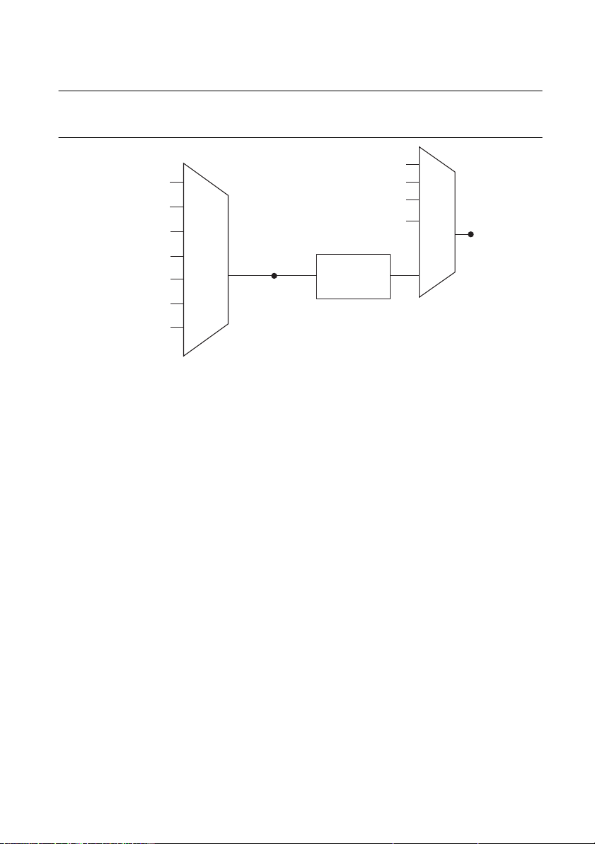
Figures 2-1 and 2-2 show the circuitry of a DIO line on Port 0 and Port 1 respectively. Each DIO
line is similar.
Figure 2-1. Digital I/O Circuitry on Port 0
DO Waveform
Generation FIFO
DO Sample Clock
Static DO
Buffer
DO.x Direction Control
CI
I/O Protection
P0.
DI Sample Clock
In both Figures 2-1 and 2-2, CI represents additional input capacitance. This capacitance
provides some filtering and slew-rate control benefits. However, the capacitance also limits the
maximum input frequency.
CI is populated on all the lines except for the default counter source input pins. CI is not
populated on the default source input pins in order to allow the measurement of higher speed
input signals. Table 2-2 lists the lines that do not populate CI. You must use the lines in Table 2-2
when measuring inputs frequencies above 25 MHz. For more information, refer to the NI 6612
Specifications.
Static DI
DI Waveform
Measurement
FIFO
DI Change
Detection
Filter
Figure 2-2. Digital I/O Circuitry on Port 1
Weak Pull-Down
2-2 | ni.com
Page 16

NI 6612 User Manual
Table 2-2. Lines Without a Populated CI
Port 0 Port 1
PFI 11 / P0.11 PFI 35 / P1.3
PFI 15 / P0.15 PFI 39 / P1.7
PFI 19 / P0.19 —
PFI 23 / P0.23 —
PFI 27 / P0.27 —
PFI 31 / P0.31 —
For voltage input and output levels and the current drive levels of the DIO lines, refer to the
NI 6612 Specifications.
Digital Input Data Acquisition Methods
When performing digital input measurements, you either can perform software-timed or
hardware-timed acquisitions.
Software-Timed Acquisitions
With a software-timed acquisition, software controls the rate of the acquisition. Software sends
a separate command to the hardware to initiate each acquisition. In NI-DAQmx, software-timed
acquisitions are referred to as having on-demand timing. Software-timed acquisitions are also
referred to as immediate or static acquisitions and are typically used for reading a single sample
of data.
Each of the DIO lines can be used as a static DI or DO line. You can use static DIO lines to
monitor or control digital signals. Each DIO can be individually configured as a digital input
(DI) or digital output (DO).
All samples of static DI lines and updates of static DO lines are software-timed.
Hardware-Timed Acquisitions
With hardware-timed acquisitions, a digital hardware signal (di/SampleClock) controls the rate
of the acquisition. This signal can be generated internally on your device or provided externally.
Hardware-timed acquisitions have several advantages over software-timed acquisitions.
• The time between samples can be much shorter.
• The timing between samples is deterministic.
• Hardware-timed acquisitions can use hardware triggering.
© National Instruments | 2-3
Page 17

Chapter 2 Digital I/O
Hardware-timed operations can be buffered or hardware-timed single point. A buffer is a
temporary storage in computer memory for to-be-transferred samples.
• Buffered—Data is moved from the DAQ device’s onboard FIFO memory to a PC buffer
using DMA before it is transferred to application memory. Buffered acquisitions typically
allow for much faster transfer rates than non-buffered acquisitions because data is moved
in large blocks, rather than one point at a time.
One property of buffered I/O operations is the sample mode. The sample mode can be either
finite or continuous:
– Finite sample mode acquisition refers to the acquisition of a specific, predetermined
number of data samples. After the specified number of samples has been read in, the
acquisition stops. If you use a reference trigger, you must use finite sample mode.
– Continuous acquisition refers to the acquisition of an unspecified number of samples.
Instead of acquiring a set number of data samples and stopping, a continuous
acquisition continues until you stop the operation. Continuous acquisition is also
referred to as double-buffered or circular-buffered acquisition.
If data cannot be transferred across the bus fast enough, the FIFO becomes full. New
acquisitions will overwrite data in the FIFO before it can be transferred to host
memory. The device generates an error in this case. With continuous operations, if the
user program does not read data out of the PC buffer fast enough to keep up with the
data transfer, the buffer could reach an overflow condition, causing an error to be
generated.
• Hardware-timed single point (HWTSP)—Typically, HWTSP operations are used to read
single samples at known time intervals. While buffered operations are optimized for high
throughput, HWTSP operations are optimized for low latency and low jitter. In addition,
HWTSP can notify software if it falls behind hardware. These features make HWTSP ideal
for real time control applications. HWTSP operations, in conjunction with the wait for next
sample clock function, provide tight synchronization between the software layer and the
hardware layer.
Refer to the document, NI-DAQmx Hardware-Timed Single Point Lateness Checking, for
more information. To access this document, go to
daqhwtsp.
ni.com/info and enter the Info Code
Digital Input Triggering
Digital input supports three different triggering actions:
• Start trigger
• Reference trigger
• Pause trigger
Refer to the DI Start Trigger Signal, DI Reference Trigger Signal, and DI Pause Trigger Signal
sections for information about these triggers.
2-4 | ni.com
Page 18
NI 6612 User Manual
PFI, RTSI, PXI_Trigger
PXI_STA R
20 MHz Timebase
100 kHz Timebase
PXI_CLK10
Programmable
Clock
Divider
DI Sample Clock
Timebase
PFI, RTSI, PXI_Trigger
PXI_STA R
Ctr n Internal Output
DI Sample Clock
100 MHz Timebase
DSTAR <A..B>
DSTAR <A..B>
Digital Waveform Acquisition
Figure 2-3 summarizes all of the timing options provided by the digital input timing engine.
Figure 2-3. Digital Input Timing Options
You can acquire digital waveforms on the Port 0 DIO lines. The DI waveform acquisition FIFO
stores the digital samples. The NI 6612 has a DMA controller dedicated to moving data from the
DI waveform acquisition FIFO to system memory. The device samples the DIO lines on each
rising or falling edge of a clock signal, DI Sample Clock.
You can configure each DIO line to be an output, a static input, or a digital waveform acquisition
input.
The following digital input timing signals are featured:
• DI Sample Clock Signal*
• DI Sample Clock Timebase Signal
• DI Start Trigger Signal*
• DI Reference Trigger Signal*
• DI Pause Trigger Signal*
Signals with an * support digital filtering. Refer to the PFI Filters section of Chapter 4, PFI, for
more information.
DI Sample Clock Signal
The device uses the DI Sample Clock (di/SampleClock) signal to sample the Port 0 terminals
and store the result in the DI waveform acquisition FIFO.
By default, the programmable clock divider drives DI Sample Clock (see Figure 2-3). You can
route many signals to DI Sample Clock. To view the complete list of possible routes, see the
© National Instruments | 2-5
Page 19
Chapter 2 Digital I/O
DI Sample Clock Timebase
DI Start Trigger
DI Sample Clock
Delay
from
Start
Trigger
Device Routes tab in MAX. Refer to Device Routing in MAX in the NI-DAQmx Help or the
LabVIEW Help for more information.
If the NI 6612 receives a DI Sample Clock when the FIFO is full, it reports an overflow error to
the host software.
You can sample data on the rising or falling edge of DI Sample Clock.
Routing DI Sample Clock to an Output Terminal
You can route DI Sample Clock out to any PFI <0..39> terminal. The PFI circuitry inverts the
polarity of DI Sample Clock before driving the PFI terminal.
Other Timing Requirements
The NI 6612 only acquires data during an acquisition. The device ignores DI Sample Clock
when a measurement acquisition is not in progress. During a measurement acquisition, you can
cause the device to ignore DI Sample Clock using the DI Pause Trigger signal.
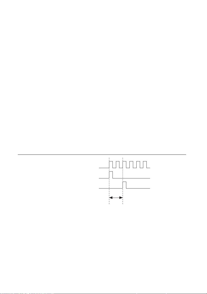
The DI timing engine on the device internally generates DI Sample Clock unless you select some
external source. DI Start Trigger starts this timing engine and either software or hardware can
stop it after a finite acquisition completes. When using the DI timing engine, you also can specify
a configurable delay from DI Start Trigger to the first DI Sample Clock pulse.
By default, this delay is set to two ticks of the DI Sample Clock Timebase signal.
Figure 2-4. DI Sample Clock and DI Start Trigger
DI Sample Clock Timebase Signal
By default, the NI 6612 routes the onboard 100 MHz timebase to DI Sample Clock Timebase.
You can route many signals to DI Sample Clock Timebase. To view the complete list of possible
routes, see the Device Routes tab in MAX. Refer to Device Routing in MAX in the NI-DAQmx
Help or the LabVIEW Help for more information.
DI Sample Clock Timebase is not available as an output on the I/O connector. DI Sample Clock
Timebase is divided down to provide one of the possible sources for DI Sample Clock. The
2-6 | ni.com
Page 20

NI 6612 User Manual
DI Start Trigger
DI Sample Clock
polarity selection for DI Sample Clock Timebase can be configured as either rising—or
falling—edge except for the 100 MHz Timebase or 20 MHz Timebase.
The DI Sample Clock Timebase may be used if an external sample clock signal is required, but
the signal needs to be divided down. If an external sample clock signal is required, but there is
no need to divide the signal, then the DI Sample Clock should be used instead of the DI Sample
Clock Timebase.
DI Start Trigger Signal
Use the DI Start Trigger (di/StartTrigger) signal to begin a measurement acquisition. A
measurement acquisition consists of one or more samples. If triggers are not used, a
measurement acquisition can be initiated with a software command. After the acquisition begins,
configure the acquisition to stop:
• When a certain number of points are sampled (in finite mode)
• After a hardware reference trigger (in finite mode)
• With a software command (in continuous mode)
An acquisition that uses a start trigger (but not a reference trigger) is sometimes referred to as a
posttriggered acquisition.
Retriggerable DI
The DI Start Trigger can also be configured to be retriggerable. The timing engine generates
samples and converts clocks for the configured acquisition in response to each pulse on an
DI Start Trigger signal.
The timing engine ignores the DI Start Trigger signal while the clock generation is in progress.
After the clock generation is finished, the timing engine waits for another Start Trigger to begin
another clock generation. Figure 2-5 shows a retriggerable DI of four samples.
Reference triggers are not retriggerable.
Figure 2-5. Retriggerable DI
Note Waveform information from LabVIEW does not reflect the delay between
triggers. They are treated as a continuous acquisition with constant t0 and dt
information.
© National Instruments | 2-7
Page 21

Chapter 2 Digital I/O
Using a Digital Source
To use DI Start Trigger with a digital source, specify a source and an edge. You can route many
signals to DI Start Trigger. To view the complete list of possible routes, see the Device Routes
tab in MAX. Refer to Device Routing in MAX in the NI-DAQmx Help or the LabVIEW Help for
more information.
You also can specify whether the measurement acquisition begins on the rising- or falling-edge
of DI Start Trigger.
Routing DI Start Trigger to an Output Terminal
You can route DI Start Trigger out to any PFI <0..39>, RTSI <0..7>, PXI_Trig <0..7>, or
PXIe-DSTARC terminal. The output is an active high pulse. All PFI terminals are configured as
inputs by default.
The device also uses DI Start Trigger to initiate pretriggered DAQ operations. In most
pretriggered applications, a software trigger generates DI Start Trigger. Refer to the
DI Reference Trigger Signal section for a complete description of the use of DI Start Trigger and
DI Reference Trigger in a pretriggered acquisition operation.
DI Reference Trigger Signal
Use the DI Reference Trigger (di/ReferenceTrigger) signal to stop a measurement acquisition.
To use a reference trigger, specify a buffer of finite size and a number of pretrigger samples
(samples that occur before the reference trigger). The number of posttrigger samples (samples
that occur after the reference trigger) desired is the buffer size minus the number of pretrigger
samples.
After the acquisition begins, the device writes samples to the buffer. After the device captures
the specified number of pretrigger samples, it begins to look for the reference trigger condition.
If the reference trigger condition occurs before the device captures the specified number of
pretrigger samples, it ignores the condition.
If the buffer becomes full, the device continuously discards the oldest samples in the buffer to
make space for the next sample. This data can be accessed (with some limitations) before the
device discards it. Refer to the KnowledgeBase document, Can a Pretriggered Acquisition be
Continuous?, for more information. To access this KnowledgeBase, go to
enter the Info Code
2-8 | ni.com
rdcanq.
ni.com/info and
Page 22

NI 6612 User Manual
Reference Trigger
Pretrigger Samples
Complete Buffer
Posttrigger Samples
When the reference trigger occurs, the device continues to write samples to the buffer until the
buffer contains the number of posttrigger samples desired. Figure 2-6 shows the final buffer.
Figure 2-6. Reference Trigger Final Buffer
Using a Digital Source
To use DI Reference Trigger with a digital source, specify a source and an edge. You can route
many signals to DI Reference Trigger. To view the complete list of possible routes, see the
Device Routes tab in MAX. Refer to Device Routing in MAX in the NI-DAQmx Help or the
LabVIEW Help for more information.
You also can specify whether the measurement acquisition stops on the rising- or falling-edge of
DI Reference Trigger.
Routing DI Reference Trigger Signal to an Output Terminal
DI Reference Trigger can be routed out to any PFI <0..39>, RTSI <0..7>, PXI_Trig <0..7>, or
PXIe-DSTARC terminal. All PFI terminals are configured as inputs by default.
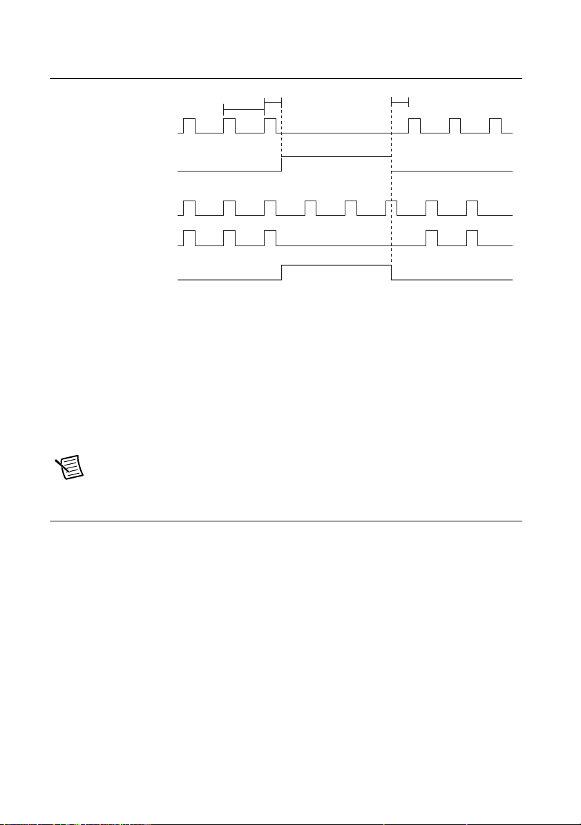
DI Pause Trigger Signal
The DI Pause Trigger (di/PauseTrigger) signal can be used to pause and resume a measurement
acquisition. The internal sample clock pauses while the external trigger signal is active and
resumes when the signal is inactive. The active level of the pause trigger can be programmed to
be high or low, as shown in Figure 2-7. In the figure, T represents the period, and A represents
the unknown time between the clock pulse and the posttrigger.
© National Instruments | 2-9
Page 23
Chapter 2 Digital I/O
Figure 2-7. Halt (Internal Clock) and Free Running (External Clock)
DI Sample Clock
DI Pause Trigger
DI External Sample Clock
DI Sample Clock
DI Pause Trigger
A
T
Halt. Used on Internal Clock
Free Running. Used on External Clock
T – A
Using a Digital Source
To use DI Pause Trigger, specify a source and a polarity. You can route many signals to DI Pause
Trigger. To view the complete list of possible routes, see the Device Routes tab in MAX. Refer
to Device Routing in MAX in the NI-DAQmx Help or the LabVIEW Help for more information.
Routing DI Pause Trigger Signal to an Output Terminal
DI Pause Trigger can be routed out to any RTSI <0..7>, PXI_Trig <0..7>, PFI <0..39>,
PXI_STAR, or PXIe-DSTARC terminal.
Note Pause triggers are only sensitive to the level of the source, not the edge.
Digital Output Data Generation Methods
When performing a digital waveform operation, either software-timed or hardware-timed
generations can be performed.
Software-Timed Generations
With a software-timed generation, software controls the rate at which data is generated. Software
sends a separate command to the hardware to initiate each update. In NI-DAQmx,
software-timed generations are referred to as on-demand timing. Software-timed generations are
also referred to as immediate or static operations. They are typically used for writing a single
value out, such as a constant digital value.
2-10 | ni.com
Page 24

NI 6612 User Manual
Hardware-Timed Generations
With a hardware-timed generation, a digital hardware signal controls the rate of the generation.
This signal can be generated internally on your device or provided externally.
Hardware-timed generations have several advantages over software-timed generations:
• The time between samples can be much shorter.
• The timing between samples can be deterministic.
• Hardware-timed acquisitions can use hardware triggering.
Hardware-timed operations can be buffered or hardware-timed single point (HWTSP). A buffer
is a temporary storage in computer memory for to-be-transferred samples.
• Hardware-timed single point (HWTSP)—Typically, HWTSP operations are used to
write single samples at known time intervals. While buffered operations are optimized for
high throughput, HWTSP operations are optimized for low latency and low jitter. In
addition, HWTSP can notify software if it falls behind hardware. These features make
HWTSP ideal for real time control applications. HWTSP operations, in conjunction with
the wait for next sample clock function, provide tight synchronization between the software
layer and the hardware layer. Refer to the document, NI-DAQmx Hardware-Timed Single
Point Lateness Checking, for more information. To access this document, go to
and enter the Info Code daqhwtsp.
info
• Buffered—In a buffered generation, data is moved from a PC buffer to the device’s
onboard FIFO using DMA before it is written to the output lines one sample at a time.
Buffered generation typically allow for much faster transfer rates than non-buffered
acquisitions because data is moved in large blocks, rather than one point at a time.
One property of buffered I/O operations is the sample mode. The sample mode can be either
finite or continuous:
– Finite sample mode generation refers to the generation of a specific, predetermined
number of data samples. After the specified number of samples has been written out,
the generation stops.
– Continuous generation refers to the generation of an unspecified number of samples.
Instead of generating a set number of data samples and stopping, a continuous
generation continues until you stop the operation. There are several different methods
of continuous generation that control what data is written. These methods are
regeneration, FIFO regeneration, and non-regeneration modes:
• Regeneration is the repetition of the data that is already in the buffer. Standard
regeneration is when data from the PC buffer is continually downloaded to the
FIFO to be written out. New data can be written to the PC buffer at any time
without disrupting the output. Use the NI-DAQmx write property regenMode to
allow (or not allow) regeneration. The NI-DAQmx default is to allow
regeneration.
• With non-regeneration, old data is not repeated. New data must be continually written
to the buffer. If the program does not write new data to the buffer at a fast enough rate
to keep up with the generation, the buffer underflows and causes an error.
ni.com/
© National Instruments | 2-11
Page 25

Chapter 2 Digital I/O
• With FIFO regeneration, the entire buffer is downloaded to the FIFO and
regenerated from there. After the data is downloaded, new data cannot be written
to the FIFO. To use FIFO regeneration, the entire buffer must fit within the FIFO
size. The advantage of using FIFO regeneration is that it does not require
communication with the main host memory after the operation is started, thereby
preventing any problems that may occur due to excessive bus traffic. Use the
NI-DAQmx DO channel property, UseOnlyOnBoardMemory to enable or
disable FIFO regeneration.
Digital Output Triggering
Digital output supports two different triggering actions:
• Start trigger
• Pause trigger
A digital trigger can initiate these actions. Refer to the DO Start Trigger Signal and DO Pause
Trigger Signal sections for more information about these triggering actions.
Digital Waveform Generation
Digital waveforms can be generated on the Port 0 DIO lines. The DO waveform generation FIFO
stores the digital samples. NI 6612 has a DMA controller dedicated to moving data from the
system memory to the DO waveform generation FIFO. The device moves samples from the
FIFO to the DIO terminals on each rising—or falling—edge of a clock signal, DO Sample
Clock. Each DIO signal is configurable to be an input, a static output, or a digital waveform
generation output.
The FIFO supports a retransmit mode. In the retransmit mode, after all the samples in the FIFO
have been clocked out, the FIFO begins outputting all of the samples again in the same order.
For example, if the FIFO contains five samples, the pattern generated consists of sample #1, #2,
#3, #4, #5, #1, #2, #3, #4, #5, #1, and so on.
The following DO (waveform generation) timing signals are featured:
• DO Sample Clock Signal*
• DO Sample Clock Timebase Signal
• DO Start Trigger Signal*
• DO Pause Trigger Signal*
Signals with an * support digital filtering. Refer to the PFI Filters section of Chapter 4, PFI, for
more information.
2-12 | ni.com
Page 26

NI 6612 User Manual
DO Sample Clock Signal
The device uses the DO Sample Clock (do/SampleClock) signal to update the DO terminals with
the next sample from the DO waveform generation FIFO. If the device receives a DO Sample
Clock when the FIFO is empty, it reports an underflow error to the host software.
By default, the NI 6612 routes the divided down DO Sample Clock Timebase to DO Sample
Clock. You can route many other signals to DO Sample Clock. To view the complete list of
possible routes, see the Device Routes tab in MAX. Refer to Device Routing in MAX in the
NI-DAQmx Help or the LabVIEW Help for more information.
Routing DO Sample Clock to an Output Terminal
DO Sample Clock can be routed out to any PFI <0..39>, RTSI <0..7>, PXI_Trig <0..7>, or
PXIe-DSTARC terminal.
Other Timing Requirements
The DO timing engine internally generates DO Sample Clock unless configured to an external
source. DO Start Trigger starts the timing engine and either the software or hardware can stop it
after a finite generation completes. When using the DO timing engine, a configurable delay can
be configured from DO Start Trigger to the first DO Sample Clock pulse. By default, this delay
is two ticks of DO Sample Clock Timebase. Figure 2-8 shows the relationship of DO Sample
Clock to DO Start Trigger.
Figure 2-8. DO Sample Clock and DO Start Trigger
DO Sample Clock Timebase
DO Start Trigger
DO Sample Clock
Delay
from
Start
Trigger
DO Sample Clock Timebase Signal
The DO Sample Clock Timebase (do/SampleClockTimebase) signal is divided down to provide
a source for DO Sample Clock. By default, the NI 6612 routes the onboard 100 MHz timebase
to the DO Sample Clock Timebase. You can route many signals to DO Sample Clock Timebase.
To view the complete list of possible routes, see the Device Routes tab in MAX. Refer to Device
Routing in MAX in the NI-DAQmx Help or the LabVIEW Help for more information.
DO Sample Clock Timebase is not available as an output on the I/O connector.
© National Instruments | 2-13
Page 27
Chapter 2 Digital I/O
DO Start Trigger
DO Sample Clock
You might use DO Sample Clock Timebase if you want to use an external sample clock signal,
but need to divide the signal down. If you want to use an external sample clock signal but do not
need to divide the signal, then you should use DO Sample Clock rather than DO Sample Clock
Timebase.
DO Start Trigger Signal
Use the DO Start Trigger (do/StartTrigger) signal to initiate a waveform generation. If you do
not use triggers, you can begin a generation with a software command.
Retriggerable DO
The DO Start Trigger can also be configured to be retriggerable. The timing engine will generate
the sample clocks for the configured generation in response to each pulse on a DO Start Trigger
signal.
The timing engine ignores the DO Start Trigger signal while the clock generation is in progress.
After the clock generation is finished, the timing engine waits for another start trigger to begin
another clock generation. Figure 2-9 shows a retriggerable DO of four samples.
Figure 2-9. Retriggerable DO
Using a Digital Start Trigger
To use DO Start Trigger, specify a source and an edge. You can route many signals to DO Start
Trigger Signal. To view the complete list of possible routes, see the Device Routes tab in MAX.
Refer to Device Routing in MAX in the NI-DAQmx Help or the LabVIEW Help for more
information.
Waveform generation can be specified to begin either on the rising- or falling-edge of DO Start
Trigger.
Routing DO Start Trigger Signal to an Output Terminal
DO Start Trigger can be routed out to any RTSI <0..7>, PFI <0..39>, PXI_Trig <0..7>, or
PXIe-DSTARC terminal. The output is an active high pulse. PFI terminals are configured as
inputs by default.
2-14 | ni.com
Page 28

NI 6612 User Manual
Pause Trigger
Sample Clock
Pause Trigger
Sample Clock
DO Pause Trigger Signal
Use the DO Pause Trigger (do/PauseTrigger) signal to mask off samples in a DAQ sequence.
That is, when DO Pause Trigger is active, no samples occur.
DO Pause Trigger does not stop a sample that is in progress. The pause does not take effect until
the beginning of the next sample.
When generating digital output signals, the generation pauses as soon as the pause trigger is
asserted. If the sample clock source is the onboard clock, the generation resumes as soon as the
pause trigger is deasserted, as shown in Figure 2-10.
Figure 2-10. DO Pause Trigger with the Onboard Clock Source
When using any signal other than the onboard clock as the source of your sample clock, the
generation resumes as soon as the pause trigger is deasserted and another edge of the sample
clock is received, as shown in Figure 2-11.
Figure 2-11. DO Pause Trigger with Other Signal Sources
Using a Digital Pause Trigger
To use DO Pause Trigger, specify a source and a polarity. You can route many signals to DO
Pause Trigger. To view the complete list of possible routes, see the Device Routes tab in MAX.
Refer to Device Routing in MAX in the NI-DAQmx Help or the LabVIEW Help for more
information.
Routing DO Pause Trigger Signal to an Output Terminal
DO Pause Trigger can be routed out to any RTSI <0..7>, PXI_Trig <0..7>, PFI <0..39>, or
PXIe-DSTARC terminal.
© National Instruments | 2-15
Page 29
Chapter 2 Digital I/O
I/O Protection
Each DIO and PFI signal has limited protection against overvoltage, undervoltage, and
overcurrent conditions as well as ESD events. Avoid these fault conditions by following these
guidelines:
• When configuring a PFI or DIO line as an output, do not connect it to any external signal
source, ground, or power supply.
• When configuring a PFI or DIO line as an output, understand the current requirements of
the load connected to these signals. Do not exceed the specified current output limits of the
DAQ device. NI has several signal conditioning solutions for digital applications requiring
high current drive.
• When configuring a PFI or DIO line as an input, do not drive the line with voltages outside
of its normal operating range.
• Treat the DAQ device as you would treat any static sensitive device. Always properly
ground yourself and the equipment when handling the DAQ device or connecting to it.
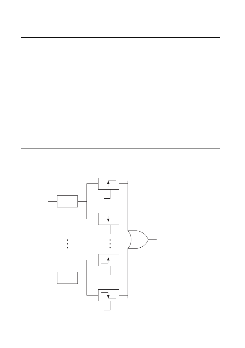
DI Change Detection
The device can be configured to detect changes in the DIO signals, which includes Port 0 and
Port 1. Figure 2-12 shows a block diagram of the DIO change detection circuitry.
Figure 2-12. DI Change Detection
P0.0
P1.7
2-16 | ni.com
Synch
Synch
Enable
Enable
Change Detection Event
Enable
Enable
Page 30

NI 6612 User Manual
The DIO change detection circuitry can be enabled to detect rising edges, falling edges, or either
edge individually on each DIO line. The device synchronizes each DI signal to the 100 MHz
Timebase, and then sends the signal to the change detectors. The circuitry ORs the output of all
enabled change detectors from every DI signal. The result of this OR is the Change Detection
Event signal.
Change detection performs bus correlation by considering all changes within a 50 ns window
one change detection event. This keeps signals on the same bus synchronized in samples and
prevents overruns.
The Change Detection Event signal can do the following:
• Drive any RTSI<0..7>, PXI_Trig<0..7>, PFI<0..39>, or PXI_STAR signal
• Drive the DO Sample Clock or DI Sample Clock
• Generate an interrupt
The Change Detection Event signal also can be used to detect changes on digital output events.
DI Change Detection Applications
The DIO change detection circuitry can interrupt a user program when one of several DIO
signals changes state.
You also can use the output of the DIO change detection circuitry to trigger a DI or counter
acquisition on the logical OR of several digital signals. By routing the Change Detection Event
signal to a counter, the relative time between bus changes can be captured.
The Change Detection Event signal can be used to trigger DO or counter generations.
Digital Filtering
A programmable debouncing filter can be enabled on each digital line on Port 0. When the filters
are enabled, the device samples the input on each rising edge of a filter clock. The device divides
down the onboard 100 MHz or 100 kHz clocks to generate the filter clock. The following is an
example of low-to-high transitions of the input signal. High-to-low transitions work similarly.
Assume that an input terminal has been low for a long time. The input terminal then changes
from low-to-high, but glitches several times. When the filter clock has sampled the signal high
on two consecutive edges and the signal remained stable in between, the low-to-high transition
is propagated to the rest of the circuit.
© National Instruments | 2-17
Page 31

Chapter 2 Digital I/O
Table 2-3. Filters
Filter Settings Filter Clocks
Pulse Width
Guaranteed to
Pass Filter
Pulse Width
Guaranteed to Not
Pass Filter
Short 12.5 MHz 160 ns 80 ns
Medium 195/3125 kHz 10.24 μs 5.12 μs
High 390.625 Hz 5.12 ms 2.56 ms
None — — —
The filter setting for each input can be configured independently. On power up, the filters are
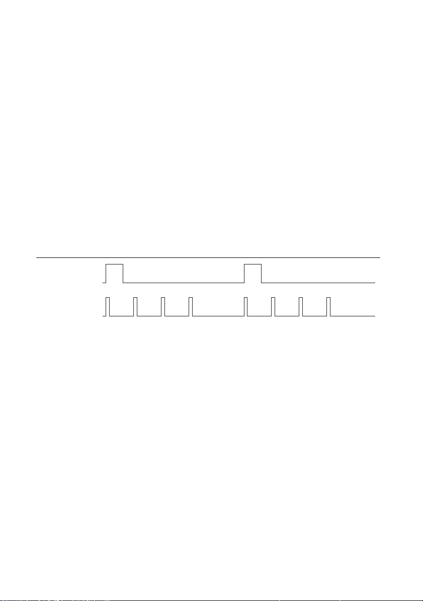
disabled. Figure 2-13 shows an example of a low-to-high transition on an input.
Figure 2-13. Input Low-to-High Transition
Digital Input P0.x
Filter Clock
11 2
Filtered Input
11 21
When multiple lines are configured with the same filter settings they are considered a bus. Two
filtering modes for use with multiple lines:
• Line filtering—Each line transitions independently of the other lines in the bus and acts
like the behavior described above
• Bus filtering—When any one line in the bus has jitter, all lines in the bus will hold state
until the bus becomes stable. However, each individual line only waits one extra filter tick
before changing. This prevents a noisy line from holding a valid transition indefinitely. If
all the bus line transitions become stable in less than one filter clock period and the bus
period is more than two filter clock periods, then all the bus lines are guaranteed to be
correlated at the output of the filter, as shown in Figure 2-13.
2-18 | ni.com
Page 32

NI 6612 User Manual
Digital Input P0.A
Digital Input P0.B
Filter Clock
Filtered Input A
Filtered Input B
Stable Stable Stable
The behavior for each transition can be thought of as a state machine. If a line transitions and
stays high for two consecutive filter clock edges, then one of two options occurs:
• Case 1—If no transitions have occurred on the other lines, the transition propagates on the
second filtered clock edge, as shown in Figure 2-14.
Figure 2-14. Case 1
• Case 2—If an additional line on the bus also has a transition during the filter clock period,
the change is not propagated until the next filter clock edge, as shown in Figure 2-15.
Figure 2-15. Case 2
Not Stable Not Stable
Digital Input P0.A
Digital Input P0.B
Filter Clock
Filtered Input A
Filtered Input B
© National Instruments | 2-19
Page 33

Chapter 2 Digital I/O
Digital Input P0.A
Digital Input P0.B
Filter Clock
Filtered Input A
Filtered Input B
1A
2A 3A
Figure 2-16 illustrates the difference between line and bus filtering.
Figure 2-16. Line and Bus Filtering
2A With line filtering, filtered input A would ignore the glitch on digital input P0.B and transition after two filter
clocks.
3A Filtered input A goes high when sampled high for two consecutive filter clocks and transitions on the next
filter edge because digital input P0.B glitches.
Connecting Digital I/O Signals
The DIO signals, P0.<0..31> and P1.<0..7> are referenced to D GND. Each line can be
individually programmed as an input or output. Figure 2-17 shows P1.<0..3> configured for
digital input and P1.<4..7> configured for digital output. Digital input applications include
receiving TTL signals and sensing external device states, such as the state of the switch shown
in the figure. Digital output applications include sending TTL signals and driving external
devices, such as the LED shown in the figure.
2-20 | ni.com
Page 34

NI 6612 User Manual
+5 V
LED
TTL Signal
+5 V
Switch
I/O Connector
D GND
Device
P1.<0..3>
P1.<4..7>
Figure 2-17. Digital I/O Connections
Caution Exceeding the maximum input voltage ratings, which are listed in the
specifications document for each NI 6612 device, can damage the device and the
computer. NI is not liable for any damage resulting from such signal connections.
Getting Started with DIO Applications in Software
The NI 6612 can be used in the following digital I/O applications:
• Static digital input
• Static digital output
• Digital waveform generation
• Digital waveform acquisition
• DI change detection
Note For more information about programming digital I/O applications and
triggers in software, refer to the NI-DAQmx Help or the LabVIEW Help.
The device uses the NI-DAQmx driver. NI-DAQmx includes a collection of programming
examples to help you get started developing an application. You can modify example code and
save it in an application. You can use examples to develop a new application or add example
code to an existing application.
© National Instruments | 2-21
Page 35

Chapter 2 Digital I/O
To locate LabVIEW, LabWindows/CVI, Measurement Studio, Visual Basic, and ANSI C
examples, refer to the KnowledgeBase document, Where Can I Find NI-DAQmx Examples?, by
going to
For additional examples, refer to zone.ni.com.
ni.com/info and entering the Info Code daqmxexp.
Signal Integrity Considerations
Refer to the Signal Integrity Considerations section in Chapter 4, PFI, for more information.
2-22 | ni.com
Page 36

3
Counters
The NI 6612 has eight general-purpose 32-bit counter/timers and a frequency generator. The
general-purpose counter/timers can be used for many measurement and pulse generation
applications. Figure 3-1 shows Counter 0 and the frequency generator. All eight counters are
identical.
Figure 3-1. Counter 0 and Frequency Generator
Input Selection Muxes
Counter 0 Source (Counter 0 Timebase)
Counter 0
Counter 0 Gate
Counter 0 Aux
Counter 0 HW Arm
Counter 0 A
Counter 0 B (Counter 0 Up_Down)
Counter 0 Z
Counter 0 Sample Clock
Input Selection Muxes
Frequency Output TimebaseFreq Out
Counters have eight input signals, although in most applications only a few inputs are used.
Each counter has a FIFO that can be used for buffered acquisition and generation. Each counter
also contains an embedded counter (Embedded Ctrn) for use in what are traditionally
two-counter measurements and generations. The embedded counters cannot be programmed
independent of the main counter, and signals from the embedded counters are not routable.
Counter measurements support several options for determining when each measurement is
taken. For example, you can configure the counter to take a measurement on each edge of a
sample clock.
Frequency Generator
Counter 0 Internal Output
Embedded Ctr0
FIFO
Counter 0 TC
For measurements using a sample clock, you must configure the NI 6612 to route a signal to the
sample clock input of the counter. The NI 6612 does not have a dedicated circuit to generate a
© National Instruments | 3-1
Page 37

Chapter 3 Counters
counter sample clock. You can route an external signal or one of many different internal signals
as the sample clock. For example, you can generate a signal using one counter and route that
signal to the sample clock of another counter. Refer to Chapter 5, Counter Signal Routing and
Clock Generation, for more information about which signals can be used as the source.
Counter Input Applications
The following sections list the various counter input applications available:
• Edge Counting
• Pulse Measurement
• Semi-Period Measurement
• Frequency Measurement
• Period Measurement
• Pulse-Width Measurement
• Two-Edge Separation
Edge Counting
In an Edge Counting measurement task, the counter counts the number of active edges of a
signal. Figure 3-2 shows an example of edge counting.
Figure 3-2. Edge Counting
Start Task
Signal to Measure
Count 105432
Channel Settings
By default, the counter:
• starts the count at 0.
• counts edges on a default PFI terminal. Refer to Chapter 5, Counter Signal Routing and
Clock Generation, for more information.
• counts rising edges.
• counts up always.
You can change these behaviors by configuring DAQmx Channel properties:
• CI.CountEdges.InitialCnt—To specify the initial value of the count.
• CI.CountEdges.Term—The signal-to-measure comes from an input terminal. To change
the signal-to-measure, specify a different terminal via this property.
3-2 | ni.com
Page 38

NI 6612 User Manual
Start Task
Signal to Measure
Count 105432
Read Value
DAQmx Read DAQmx Read
3 5
• CI.CountEdges.ActiveEdge—To specify on which edge, whether rising or falling, to
increment or decrement the counter.
• CI.CountEdges.Dir—To set whether to increment or decrement the counter on each edge.
You can set this property to:
– Count Up
– Count Down
– Externally Controlled
If you select Externally Controlled, the device monitors a hardware signal to determine the
count direction. When the signal is high, the counter counts up; when the signal is low, the
counter counts down. You can set which signal to monitor via CI.CountEdges.DirTerm.
Timing Settings
The timing settings determine when the device reads the count value.
On-Demand
By default, the counter uses On-Demand (no sample clock) timing. The counter starts counting
when software calls DAQmx Start Task. Each time you call DAQmx Read, the counter returns
the current count value. Figure 3-3 shows an example using On-Demand timing.
Figure 3-3. Edge Counting: On-Demand Timing
Sample Clock
To precisely control when the device reads the count value, use the DAQmx Timing (Sample
Clock) VI or function. With this VI or function, you can set the source of the Sample Clock, the
rate of the Sample Clock, and the number of samples to acquire.
© National Instruments | 3-3
Page 39

Chapter 3 Counters
3
6
3
Start Task
Signal to Measure
Sample Clock
Count
Buffer
10763 452
On each sample clock, the device stores the current count value in a buffer. Use DAQmx Read
to read the values from this buffer. Figure 3-4 shows an example using Sample Clock Timing.
Figure 3-4. Edge Counting: Sample Clock Timing
Trigger Settings
By default, the counter:
• begins counting when software calls DAQmx Start Task.
• counts every active edge on the input terminal.
• never resets the count until you call DAQmx Stop Task.
You can change these behaviors by configuring DAQmx Trigger properties.
Using an Arm Start Trigger
Use an Arm Start Trigger to have the counter begin counting in response to a hardware trigger.
1. Set ArmStart.TrigType to Digital Edge.
2. Set ArmStart.DigEdge.Src to select what signal to use as the ArmStartTrigger.
3. Set ArmStart.DigEdge.Edge to select the rising or falling edge of the signal.
Figure 3-5 shows an example of a count edge task using an Arm Start Trigger.
3-4 | ni.com
Figure 3-5. Edge Counting: Using an Arm Start Trigger
Start Task
Signal to Measure
Count
Arm Start Trigger Source
10 32
Page 40

NI 6612 User Manual
Start Task
Signal to Measure
Count Reset Terminal
Count
765438
69 3 54
Using a Pause Trigger
To configure the counter to pause counting based on a hardware signal, use a Pause Trigger.
1. Set Pause.TrigType to Digital Level.
2. Set Pause.DigLvl.Src to select what signal to use as the Pause Trigger.
3. Set Pause.DigLvl.When to select whether to pause counting when the signal is high or low.
Figure 3-6 shows an example of a count edge task using a Pause Trigger.
Figure 3-6. Edge Counting: Using a Pause Trigger
Start Task
Signal to Measure
Count
Pause Trigger Source
10
2
4
3
5
6
Using a Reset Trigger
To configure the counter to reset the count to a specific value in response to a hardware signal,
set the following DAQmx Channel properties:
1. Set CI.CountEdges.CountReset.Enable to True.
2. Set CI.CountEdges.CountReset.Term to select the signal that causes the count to reset.
3. Set CI.CountEdges.CountReset.ActiveEdge to select whether the rising or falling edge of
the signal causes a reset.
4. Set CI.CountEdges.ResetCnt to the value to change the count to in response to the signal.
Figure 3-7 shows an example using the Reset Trigger with CI.CountEdges.InitialCnt set to 6,
CI.CountEdges.CountReset.Active Edge set to rising edge, and CI.CountEdges.ResetCnt set
to 3.
Figure 3-7. Edge Counting: Using a Reset Trigger
© National Instruments | 3-5
Page 41

Chapter 3 Counters
Other Settings
You can filter noise on any PFI signal that is an input to the counter by enabling a filter. Refer
to the PFI Filters section in Chapter 4, PFI, for more information.
If you route the same PFI signal to multiple destinations, you should enable the Synchronization
feature. Refer to Chapter 4, PFI, for more information.
Exporting a Terminal Count Signal
Each counter, n, asserts an internal terminal count signal, CtrnInternalOutput, when the count
reaches 2^32-1 when counting up, or when the count reaches 0 when counting down.
To route the terminal count signal to an output terminal, use the CtrOutEvent.OutputTerm
DAQmx Export Signal property. You can change the polarity and other behavior of the output
signal by setting CtrOutEvent.OutputBehavior, CtrOutEvent.Pulse.Polarity, and
CtrOutEvent.Toggle.IdleState.
Cascading Counters
You can cascade two counters to make a single 64-bit counter. For example, assuming that you
want to use counter 5 and counter 6 to make a 64-bit counter, configure the following:
1. Set counter 5 to count edges.
2. Route the signal-to-measure to counter 5.
3. Configure counter 6 to count edges.
4. Route the terminal count signal of counter 5 to the input of counter 6. That is, on counter 6,
set the CI.CountEdges.Term DAQmx Channel property to Ctr5InternalOutput.
Pulse Measurement
Note This section describes Pulse measurements. For Pulse-Width measurements,
refer to the Pulse-Width Measurement section.
In a Pulse measurement task, the counter measures the high and low duration of a pulse on a
signal. You can configure DAQmx to return the high and low times of the pulse, or return the
frequency and duty cycle of the pulse. Figure 3-8 shows an example of a Pulse measurement.
3-6 | ni.com
Page 42

Signal to Measure
Counter Timebase
Start Task
Figure 3-8. Pulse Measurement
DAQmx
Read
Pulse High
Pulse
Low
Pulse
High
NI 6612 User Manual
DAQmx
Read
Pulse
Low
Count
Buffer
Read Value
10 3 122
3
000112
2
3
3
2
1
2
1
2
1
Create Channel
To make a Pulse measurement, first create a virtual channel. Use one of following three VIs or
functions depending on the type of data you want DAQmx to return:
• DAQmx Create Channel (CI-Pulse Freq)—For each measurement, return the frequency
and the duty cycle of the signal-to-measure.
• DAQmx Create Channel (CI-Pulse Time)—For each measurement, return the high and
low times of the pulse in seconds.
• DAQmx Create Channel (CI-Pulse Ticks)—For each measurement, return the high and
low times of the pulse in ticks of the counter timebase.
Channel Settings
By default, the counter:
• measures the pulse on a default PFI terminal. Refer to Chapter 5, Counter Signal Routing
and Clock Generation, for more information.
• begins measuring on a rising edge. That is, the counter measures the pulse high time first,
then the low time.
You can change these behaviors by configuring the following DAQmx Channel properties:
• The signal-to-measure comes from an input terminal. To change the signal-to-measure,
select the appropriate property from the following list that corresponds to the type of
channel created, and then set this property to a different terminal.
– CI.Pulse.Freq.Term
– CI.Pulse.Time.Term
– CI.Pulse.Ticks.Term
© National Instruments | 3-7
Page 43

Chapter 3 Counters
DAQmx
Start Task
Signal to
Meaure
Counter
Timebase
HL
4
2
HL
4
2
4
4
6
2
2
2
HL
4
2
4
4
6
2
HL
4
2
4
4
Buffer
• To specify on which edge, rising or falling, to begin the measurement, select the appropriate
property from the following list that corresponds to the type of channel created, and then
set this property to rising or falling.
– CI.Pulse.Freq.StartingEdge
– CI.Pulse.Time.StartingEdge
– CI.Pulse.Ticks.StartingEdge
Timing Settings
The timing settings determine when the device measures the signal.
On-Demand
By default, the counter uses On-Demand (no sample clock) timing. Figure 3-8 shows an
example of On-Demand timing. The following sequence of events describes On-Demand
timing:
1. Software calls DAQmx Start Task.
2. The device measures the first full pulse on the signal-to-measure.
3. The device waits until you call DAQmx Read. The device ignores the signal-to-measure
while waiting.
4. The device returns the measurement.
5. The device then measures the next full pulse on the signal-to-measure.
6. Steps 3, 4, and 5 are repeated.
Implicit
With Implicit timing, the device measures the high and low time of every pulse on the
signal-to-measure. The measurements are stored in a buffer. Each call to DAQmx Read returns
values from this buffer. Figure 3-9 shows an example using Implicit timing.
Figure 3-9. Pulse Measurement: Implicit Timing
To use Implicit timing, use the DAQmx Timing (Implicit) VI or function.
3-8 | ni.com
Page 44

NI 6612 User Manual
Sample Clock
With Sample Clock timing, on each active edge of the sample clock, the device stores one
measurement. The one measurement is the high and low pulse times of the most recent full pulse
to occur before the sample clock. Figure 3-10 shows an example using Sample Clock timing.
Figure 3-10. Pulse Measurement: Sample Clock Timing
DAQmx
Start Task
Signal to
Measure
Counter
Timebase
Sample
Clock
Buffer
Sample 1 Sample 2
HL
22 33
22
HL
2
2
3
3
To use Sample Clock timing, use the DAQmx Timing (Sample Clock) VI or function.
Trigger Settings
By default, the counter begins measuring when software calls DAQmx Start Task. You can
change this behavior by setting DAQmx Trigger properties.
To have the counter begin counting in response to a hardware trigger, use an Arm Start Trigger.
1. Set ArmStart.TrigType to Digital Edge.
2. Set ArmStart.DigEdge.Src to select which signal to use as an ArmStartTrigger.
3. Set ArmStart.DigEdge.Edge to select the rising or falling edge of the signal.
Figure 3-11 shows an example of a count edge task using an Arm Start Trigger.
Figure 3-11. Pulse Measurement: Using Arm Start Trigger
Start Task
Arm Start
Trigger
Signal to
Meaure
Counter
Timebase
Buffer
Read Value
DAQmx
2
DAQmx
Read
22
2
2
© National Instruments | 3-9
Page 45

Chapter 3 Counters
3
2
3
Start Task
Signal to Measure
Counter Timebase
Count
Buffer
10 3 122
DAQmx Read
3
Read Value
Pulse High
Pulse Low
DAQmx Read
2
Other Settings
The counter measures the pulse using the Counter Timebase signal. By default, the counter uses
an onboard 100 MHz signal as the timebase. To change the timebase, use the CI.CtrTimebaseSrc
DAQmx Channel property.
You can filter noise on any PFI signal that is an input to the counter by enabling a filter. Refer
to the PFI Filters section in Chapter 4, PFI, for more information.
If you route the same PFI signal to multiple destinations, you should enable the Synchronization
feature. Refer to Chapter 4, PFI, for more information.
Semi-Period Measurement
Semi-Period measurements are very similar to pulse measurements. Refer to the Pulse
Measurement section for more information. In hardware, both measurements are the same;
however, data is returned with a different alignment.
In a Pulse measurement each pair of high and low times is returned as one point of data—each
point of data consists of both the high time and low time. Figure 3-9 shows an example of Pulse
measurement.
In a Semi-Period measurement, the high and low times are returned as separate points.
Figure 3-12 shows an example of Semi-Period measurement.
Figure 3-12. Semi-Period Measurement
Settings
The settings available for a Semi-Period measurement are similar to those available for pulse
measurements. Refer to the Pulse Measurement section for more information. For example, use
CI.SemiPeriod.Term to change the signal-to-measure.
Pulse measurements support sample clock timing; Semi-Period measurements do not.
3-10 | ni.com
Page 46

NI 6612 User Manual
f
p
t
-- -=
Frequency Measurement
Frequency Measurement Considerations
The NI 6612 supports five methods for measuring frequency. Table 3-1 summarizes the five
frequency measurement methods.
Table 3-1. Frequency Measurement Methods
Number
Method Timing
of
Counters
Measurement
Duration
Sample Clock (with Averaging) Sample
Clock
1 Time between
two sample clock pulses
Sample Clock (without Averaging) 1 1 period of input signal
Low Frequency with 1 Counter Sample
1 1 period of input signal
Clock or
Implicit
Large Range with 2 Counters Implicit 2 P periods of input signal
High Frequency with 2 Counters 2 T time
In choosing a method, consider the measurement duration, timing, and number of counters.
Measurement duration can be either a fixed time or a fixed number of periods of the input signal.
That is, to calculate frequency, the counter can either:
• measure the number of periods (p) that occur during a specified time duration (t).
Figure 3-13 shows an example with a measurement duration of 100 µs.
• measure the time (t) it takes to observe a specified number of periods (p). Figure 3-14
shows an example with a measurement duration of three periods.
In both cases, the frequency, f, is given by:
Figure 3-13. Frequency Measurement Using Time
measurement duration = 100 µs
Counter Timebase
(100 MHz)
Signal to Measure
Count
0
1
2
50
© National Instruments | 3-11
Page 47

Chapter 3 Counters
Count
Signal to Measure
Counter Timebase
(100 MHz)
measurement duration
= 3 periods
143 562
Figure 3-14. Frequency Measurement Using Periods
Trade-offs
Consider the following trade-offs when determining the method of measuring frequency:
• Accuracy vs. Update Rate
Increasing measurement duration increases the accuracy of the measurement.
Decreasing measurement duration allows the counter to update the measurement more
often. If the input frequency changes often, it may be better to take many less-accurate
measurements than a few more accurate ones.
• Sample Clock vs. Implicit Timing
If you use a sample clock, the device returns one frequency measurement for each
sample clock.
If you use implicit timing and specify a measurement time, the device returns the
measurement after that amount of time.
If you use implicit timing and specify a number of periods to measure, the device returns
the measurement after that number of periods of the input signal. Note that the time to
return a measurement depends on the (unknown) frequency of the input signal. If the input
signal is at a low frequency, the device will take a long time to return a measurement.
• Number of Counters
Some methods use two of the eight counters on the NI 6612; other methods use one of the
eight counters.
Frequency Measurement Methods
This section describes the frequency measurement methods supported by the NI 6612.
Sample Clock (with Averaging)
With this method, for each sample clock the counter counts the number of full periods (T1) of
the signal-to-measure since the previous sample clock. It also measures the duration of these full
periods by counting the number of cycles (T2) of the timebase.
3-12 | ni.com
Page 48

NI 6612 User Manual
fxf
k
T1
T2
------×=
Maximum Error (%)
f
x
f
k
f
x
f
s
--- 1–×
----------------------------= 100 %×
Maximum Frequency Error (Hz) f
x
f
x
f
k
f
x
f
s
--- 1–×
----------------------------×=
Figure 3-15. Frequency Measurement: Sample Clock with Averaging
DAQmx
Start Task
Sample 3Sample 1
T2
7
10
T1 T2
1
2
1
Signal to
Measure (f )
Counter
Timebase (f )
Sample
Clock (f )
Buffer
Sample 2
x
k
s
121
7106
T1 T2
1
7
T1
1
2
At each sample clock, the device stores T1 and T2 in a buffer. DAQmx reads these values, and
uses the known frequency of the timebase (fk), to calculate the frequency of the input signal (fx)
as:
The maximum error and maximum frequency error for this method, are given by:
7
10
6
To use the Sample Clock (with Averaging) method, configure the following:
• DAQmx Create channel (CI-Frequency)—Use this VI or function to create the channel.
• DAQmx Timing (Sample Clock)—Use this VI or function to set the number of samples,
sample clock source, and other properties.
• CI.Freq.EnableAveraging—Set this property to True.
By default, the counter measures the frequency on a default PFI terminal (refer to Chapter 5,
Counter Signal Routing and Clock Generation, for more information) and use an onboard
100 MHz clock as the timebase. To change the signals used for this measurement, configure the
following:
• CI.Freq.Term—The signal-to-measure comes from an input terminal. To change the
signal-to-measure, set this property to a different terminal.
© National Instruments | 3-13
Page 49

Chapter 3 Counters
fxf
k
1
T2
------×=
Sample
Clock
DAQmx
Start Task
Buffer
6
646
4
6
4
6
6
Sample 1 Sample 2 Sample 3
Signal to
Measure (f )
Counter
Timebase (f )
x
k
• CI.CtrTimebase.Src—To change the signal used as the counter timebase, set this property
to a different terminal.
Sample Clock (without Averaging)
With this method, for each sample clock the counter detects the last full period of the
signal-to-measure that occurs before the sample clock. The counter measures the duration of this
one period by counting the number of cycles (T2) of the timebase.
At each sample clock, the device stores T2 in a buffer. DAQmx reads this value, and uses the
known frequency of the timebase (f
Figure 3-16. Frequency Measurement: Sample Clock without Averaging
), to calculate the frequency of the input signal (fx) as:
k
To use the Sample Clock (without Averaging) method, configure the following:
• DAQmx Create channel (CI-Frequency)—Use this VI or function to create the channel.
• DAQmx Timing (Sample Clock)—Use this VI or function to set the number of samples,
samples clock source, and other properties.
• CI.Freq.EnableAveraging—Set this property to False.
By default, the counter measures the frequency on a default PFI terminal (refer to Chapter 5,
Counter Signal Routing and Clock Generation, for more information) and use an onboard
100 MHz clock as the timebase. To change the signals used for this measurement, configure the
following:
• CI.Freq.Term—The signal-to-measure comes from an input terminal. To change the
signal-to-measure, set this property to a different terminal.
• CI.CtrTimebase.Src—To change the signals used as the counter timebase, set this
property to a different terminal.
3-14 | ni.com
Page 50

NI 6612 User Manual
f
x
f
k
T2
------=
123 … T2…
Frequency of f =
T2
Interval Measured
f
DAQmx
Start Task
x
k
Signal to
Measure (f )
Counter
Timebase (f )
x
k
Maximum Error (%)
f
x
fkfx–
-------------= 100%×
Maximum Frequency Error (Hz) f
x
f
x
fkfx–
-------------×=
Low Frequency with 1 Counter
For this method, the device detects the first full period of the signal-to-measure. The counter
measures the duration of this period by counting the number of cycles (T2) of the timebase.
DAQmx reads T2, and uses the known frequency of the timebase (fk), to calculate the frequency
of the input signal (f
Figure 3-17. Frequency Measurement: Low Frequency with One Counter
The maximum error and maximum frequency error for this method, are given by:
) as:
x
To use the Low Frequency with 1 Counter method, configure the following:
• DAQmx Create channel (CI-Frequency)—Use this VI or function to create the channel.
• CI.Freq.MeasMeth—Set this property to Low Frequency with 1 Counter.
By default, the counter measures the frequency on a default PFI terminal (refer to Chapter 5,
Counter Signal Routing and Clock Generation, for more information) and use an onboard
100 MHz clock as the timebase. To change the signals used for this measurement, configure the
following:
• CI.Freq.Term—The signal-to-measure comes from an input terminal. To change the
signal-to-measure, set this property to a different terminal.
• CI.CtrTimebase.Src—To change the signals used as the counter timebase, set this
property to a different terminal.
© National Instruments | 3-15
Page 51

Chapter 3 Counters
fxf
k
T1
T2
------
×=
Source Out
Counter N
Source
Gate
Counter M
Counter N Out
Interval
to Measure
0123 … T1
012
… T2
Signal to
Measure (f )
Counter
Timebase (f )
x
k
Signal to Measure (f )
Counter Timebase (f )
x
k
Maximum Error (%)
f
x
Nfkfx–×
----------------------- -= 100%×
Maximum Frequency Error (Hz) f
x
f
x
Nfkfx–×
----------------------- -×=
Large Range with 2 Counters
This measurement method requires two counters: Counter N and Counter M.
For this measurement method, Counter N creates a pulse equal to T1 periods of the
signal-to-measure. The device routes this pulse to Counter M. Counter M measures the duration
of this pulse by counting the number of cycles (T2) of the timebase.
The device returns T2 and T1 to DAQmx. DAQmx reads these value, and uses the known
frequency of the timebase (f
Figure 3-18. Frequency Measurement: Large Range of Frequencies with Two Counters
) to calculate the frequency (fx) of the signal-to-measure as:
k
With N as the integer that divides down the input signal (fx), which can be configured in
CI.Freq.Div, the maximum error and maximum frequency error for this method are given by:
3-16 | ni.com
Page 52

NI 6612 User Manual
T
P
f
x
---=
f
x
P
T
---=
To use the Large Range with 2 Counters method, configure the following:
• DAQmx Create channel (CI-Frequency)—Use this VI or function to create the channel.
• CI.Freq.MeasMeth—Set this property to Large Range with 2 Counters.
Note that this measurement method requires two counters:
• Counter 0 paired with Counter 1
• Counter 2 paired with Counter 3
• Counter 4 paired with Counter 5
• Counter 6 paired with Counter 7
By default, the counters measure the frequency on a default PFI terminal (refer to Chapter 5,
Counter Signal Routing and Clock Generation, for more information) and use an onboard
100 MHz clock as the timebase. To change the signals used for this measurement, configure the
following:
• CI.Freq.Term—The signal-to-measure comes from an input terminal. To change the
signal-to-measure, set this property to a different terminal.
• CI.CtrTimebase.Src—To change the signals used as the counter timebase, set this
property to a different terminal.
High Frequency with 2 Counters
This measurement method requires two counters: Counter N and Counter M.
For this measurement method, the devices uses counter M to generate a pulse of duration T. The
device routes this pulse to Counter N. Counter N then counts the number of periods (P) of the
signal-to-measure during the pulse.
If the frequency of the signal-to-measure is fx, the duration of the pulse is given by:
Solving for fx returns the frequency of the signal-to-measure:
© National Instruments | 3-17
Page 53

Chapter 3 Counters
Maximum Error (%)
1
Tfx×
-------------= 100%×
Maximum Frequency Error (Hz)
1
T
-- -=
Figure 3-19. Frequency Measurement: High Frequency with Two Counters
Counter
Timebase (f )
Signal to
Measure
Pulse
Signal to
Measure (f )
Source Out
k
Counter M
Source
Gate
T
12… P
x
Counter N
Pulse
With the known measurement time (T), which can be configured in CI.Freq.MeasTime, the
maximum error and maximum frequency error for this method are given by:
To use the High Frequency with 2 Counters method, configure the following:
• DAQmx Create channel (CI-Frequency)—Use this VI or function to create the channel.
• CI.Freq.MeasMeth—Set this property to High Frequency with 2 Counters
Note that this measurement method requires two counters:
• Counter 0 paired with Counter 1
• Counter 2 paired with Counter 3
• Counter 4 paired with Counter 5
• Counter 6 paired with Counter 7
3-18 | ni.com
Page 54

NI 6612 User Manual
By default, the counters measure the frequency on a default PFI terminal (refer to Chapter 5,
Counter Signal Routing and Clock Generation, for more information) and use an onboard
100 MHz clock as the timebase. To change the signals used for this measurement, configure the
following:
• CI.Freq.Term—The signal-to-measure comes from an input terminal. To change the
signal-to-measure, set this property to a different terminal.
• CI.CtrTimebase.Src—To change the signals used as the counter timebase, set this
property to a different terminal.
Period Measurement
Period measurements return the inverse result of Frequency measurements. Refer to the
Frequency Measurement section for more information.
The settings available for Period measurements are similar to Frequency measurements. For
example, use CI.Period.Term to change the signal-to-measure.
Pulse-Width Measurement
Note This section describes Pulse-Width measurements. For Pulse measurements,
refer to the Pulse Measurement section.
In a Pulse-Width measurement task, the counter measures the duration of a pulse on a signal.
Figure 3-20 shows an example of a Pulse-Width measurement.
Figure 3-20. Pulse-Width Measurement
DAQmx
Start Task
Sample
DAQmx Read
Signal to Measure
Counter Timebase
10
Counter Value
Read Value
2
2
The Pulse-Width can be calculated based on the number of edges of the Counter Timebase that
occur during the pulse on the signal-to-measure. This measurement begins when the
signal-to-measure first enters the active state. If the counter is armed while the signal-to-measure
is already in the active state, then the counter will wait for the next transition to the active state
to begin the measurement.
© National Instruments | 3-19
Page 55

Chapter 3 Counters
Channel Settings
By default, the counter:
• measures pulses on a default PFI terminal. Refer to Chapter 5, Counter Signal Routing and
Clock Generation, for more information.
• measures a high pulse. That is, the counter begins measuring the time from a rising edge to
the next falling edge.
• returns the measurement in the unit of seconds.
You can change these behaviors by configuring DAQmx Channel properties:
• CI.PulseWidth.Term—The signal-to-measure comes from an input terminal. To change
the signal-to-measure, set this property to a different terminal.
• CI.PulseWidth.StartingEdge—Specifies on which edge, rising or falling, to begin the
measurement.
• CI.PulseWidth.Units—Specifies the units of the measurement.
Timing Settings
The timing settings determine when the device measures the signal. Figure 3-20 shows an
example of On-Demand timing.
On-Demand (No Sample Clock)
By default, the counter uses On-Demand timing. The following sequence of events describe On
Demand timing:
1. Software calls DAQmx Start Task.
2. The device measures the first full pulse on the signal-to-measure.
3. The device waits until you call DAQmx Read. The device ignores the signal-to-measure
while waiting.
4. The device returns the measurement.
5. The device then measures the next full pulse on the signal-to-measure.
6. Steps 3, 4, and 5 are repeated.
3-20 | ni.com
Page 56

NI 6612 User Manual
Signal to
Measure
Counter
Timebase
Sample Clock
2 342
4
3
22
4
Buffer
Sample
Sample
Implicit
With Implicit timing, the device measures the time of every pulse on the signal-to-measure. The
measurements are stored in a buffer. Each call to DAQmx Read returns values from this buffer.
Figure 3-21 shows an example of Implicit timing.
Figure 3-21. Pulse-Width Measurement: Implicit Timing
DAQmx Start Task
Arm Start Trigger
Signal to Measure
Counter Timebase
Counter Value
Buffer
0
21
2
21 3
2
3
To use Implicit timing, use the DAQmx Timing (Implicit) VI or function.
Sample Clock
With Sample Clock timing, on each active edge of the sample clock, the device stores one
measurement. The one measurement is the pulse time of the most recent full pulse to occur
before the sample clock. Figure 3-22 shows an example of Sample Clock timing.
Figure 3-22. Pulse-Width Measurement: Sample Clock
To use Sample Clock timing, use the DAQmx Timing (Sample Clock) VI or function.
Trigger Settings
By default, the counter begins measuring when software calls DAQmx Start Task. You can
change this behavior by setting DAQmx Trigger properties.
To have the counter begin counting in response to a hardware trigger, use an Arm Start Trigger.
1. Set ArmStart.TrigType to Digital Edge.
2. Set ArmStart.DigEdge.Src to select which signal to use as the ArmStartTrigger.
3. Set ArmStart.DigEdge.Edge to select the rising or falling edge of the signal.
© National Instruments | 3-21
Page 57

Chapter 3 Counters
Counter Timebase
Signal to Measure
Counter Value
Buffer
0
21
DAQmx Start Task
2
21 3
2
3
Arm Start Trigger
First Signal
DAQmx
Start Task
000123 45678
Measured Interval
Second Signal
Counter Timebase
Counter Value
Latched Value
0
8
DAQmx
Read
Figure 3-23 shows an example of a Pulse-Width measurement using an Arm Start Trigger. Note
that if the counter is armed while the signal-to-measure is already in the active state, the counter
will wait to perform the measurement on the next full pulse after the Arm Start Trigger.
Figure 3-23. Pulse-Width Measurement: Using the Arm Start Trigger
Other Settings
The counter measures the pulse using the Counter Timebase signal. By default, the counter uses
an onboard 100 MHz signal as the timebase. To change the timebase, use the CI.CtrTimebaseSrc
DAQmx Channel property.
You can filter noise on any PFI signal that is an input to the counter by enabling a filter. Refer
to the PFI Filters section in Chapter 4, PFI, for more information.
If you route the same PFI signal to multiple destinations, you should enable the Synchronization
feature. Refer to Chapter 4, PFI, for more information.
Two-Edge Separation
In a Two-Edge Separation measurement task, the counter measures the time between two events.
The beginning event is an active edge on a first signal. The ending event is an active edge on a
second signal. Figure 3-24 shows an example of a Two-Edge Separation measurement.
3-22 | ni.com
Figure 3-24. Two-Edge Separation Measurement
Page 58

NI 6612 User Manual
Channel Settings
By default, the counter:
• monitors for events on default PFI terminals. Refer to Chapter 5, Counter Signal Routing
and Clock Generation, for more information.
• looks for rising edges on the first signal and second signal.
• returns the measurement in the unit of seconds.
You can change these behaviors by configuring DAQmx Channel properties:
• CI.TwoEdgeSep.First.Term—The signal that the device monitors for the beginning event
comes from an input terminal. To change the signal to monitor, set this property to a
different terminal.
• CI.TwoEdgeSep.Second.Term—To change the signal to monitor for the ending event, set
this property to a different terminal.
• CI.TwoEdgeSep.First.Edge—Specifies on which edge of the first signal, rising or falling,
the device begins the measurement.
• CI.TwoEdgeSep.Second.Edge—Specifies on which edge of the second signal, rising or
falling, the device ends the measurement
• CI.TwoEdgeSep.Units—Specifies the units of the measurement.
Timing Settings
The timing settings determine when the device measures the signal. Figure 3-24 shows an
example of On-Demand timing.
On-Demand (No sample clock)
By default, the counter uses On-Demand timing. The following sequence of events describe
On-Demand timing:
1. Software calls DAQmx Start Task.
2. The device measures the time between the beginning and ending events.
3. The device waits until you call DAQmx Read. The device ignores the signals while waiting.
4. The device returns the measurement.
5. The device then detects the next beginning and ending events to make a new measurement.
6. Steps 3, 4, and 5 are repeated.
Implicit Timing
With Implicit timing, the device measures the time between every pair of beginning and ending
events. The measurements are stored in a buffer. Each call to DAQmx Read returns values from
this buffer. Figure 3-25 shows an example of Implicit timing.
© National Instruments | 3-23
Page 59

Chapter 3 Counters
Counter Timebase
Counter Value
Buffer
First Signal
Second Signal
123 123 123
3
3
3
3
3
3
Counter Timebase
Counter Value
Buffer
First Signal
Second Signal
123 123
3 3
3
Sample
Clock
Figure 3-25. Two-Edge Separation Measurement: Implicit Timing
To use Implicit timing, use the DAQmx Timing (Implicit) VI or function.
Sample Clock
With Sample Clock timing, on each active edge of the sample clock, the device stores one
measurement. The one measurement is the time between the most recent pair of beginning and
ending events to occur before the sample clock. Figure 3-26 shows an example of Sample Clock
timing.
Figure 3-26. Two-Edge Separation Measurement: Sample Clock Timing
To use Sample Clock timing, use the DAQmx Timing (Sample Clock) VI or function.
Trigger Settings
By default, the counter begins measuring when software calls DAQmx Start Task. You can
change this behaviors by setting DAQmx Trigger properties.
To have the counter begin measuring in response to a hardware trigger, use an Arm Start Trigger.
1. Set ArmStart.TrigType to Digital Edge.
2. Set ArmStart.DigEdge.Src to select which signal to use as the ArmStartTrigger.
3. Set ArmStart.DigEdge.Edge to select the rising or falling edge of the signal.
3-24 | ni.com
Page 60

NI 6612 User Manual
Ch A
Ch B
Counter Value
7 7 6 5
5
6
Other Settings
The counter measures time using the Counter Timebase signal. By default, the counter uses an
onboard 100 MHz signal as the timebase. To change the timebase, use the CI.CtrTimebaseSrc
DAQmx Channel property.
You can filter noise on any PFI signal that is an input to the counter by enabling a filter. Refer
to the PFI Filters section in Chapter 4, PFI, for more information.
If you route the same PFI signal to multiple destinations, you should enable the Synchronization
feature. Refer to Chapter 4, PFI, for more information.
Quadrature and Two-Pulse Encoder Overview
The NI 6612 can make angular and linear position measurements using quadrature and
two-pulse encoders.
Quadrature Encoders
A quadrature encoder can have up to three channels: channels A, B, and Z. When channel A
leads channel B in a quadrature cycle, the counter increments. When channel B leads channel A
in a quadrature cycle, the counter decrements. The amount of increments and decrements per
cycle depends on the type of encoding: X1, X2, or X4.
• X1 Encoding—Figure 3-27 shows a quadrature cycle and the resulting increments and
decrements for X1 encoding. When channel A leads channel B, the increment occurs on the
rising edge of channel A. When channel B leads channel A, the decrement occurs on the
falling edge of channel A.
Figure 3-27. X1 Encoding
• X2 Encoding—The counter increments or decrements on each edge of channel A,
depending on which channel leads the other. Each cycle results in two increments or
decrements, as shown in Figure 3-28.
Figure 3-28. X2 Encoding
Ch A
Ch B
Counter Value
56 8 97 56
9 7
8
• X4 Encoding—The counter increments or decrements on each edge of channels A and B.
Whether the counter increments or decrements depends on which channel leads the other.
Each cycle results in four increments or decrements, as shown in Figure 3-29.
© National Instruments | 3-25
Page 61

Chapter 3 Counters
Ch A
Ch B
Figure 3-29. X4 Encoding
Counter Value5 6 8 910 1011 1112 1213 137
568 79
Channel Z Behavior
Some quadrature encoders have a third channel, channel Z, which is also referred to as the index
channel. A high level on channel Z causes the counter to be reloaded with a specified value in a
specified phase of the quadrature cycle. Depending on configuration, this reload can occur in any
one of the four phases in a quadrature cycle.
Channel Z behavior—when it goes high and how long it stays high—differs with quadrature
encoder designs. Refer to the documentation for your quadrature encoder to obtain timing of
channel Z with respect to channels A and B. You must then ensure that channel Z is high during
at least a portion of the phase you specify for reload.
In Figure 3-30, the reload phase is when both channel A and channel B are low. The reload
occurs when this phase is true and channel Z is high. Incrementing and decrementing takes
priority over reloading. Thus, when the channel B goes low to enter the reload phase, the
increment occurs first. The reload occurs within one maximum timebase period after the reload
phase becomes true. After the reload occurs, the counter continues to count as before. The figure
illustrates channel Z reload with X4 decoding.
Figure 3-30. Channel Z Reload with X4 Decoding
Ch A
Ch B
Ch Z
Max Timebase
Counter Value
56
8 90 21743
A = 0
B = 0
Z = 1
3-26 | ni.com
Page 62

NI 6612 User Manual
Ch A
Ch B
Counter Value2 3 54 344
Two-Pulse Encoders
The counter supports two pulse encoders that have two channels: channels A and B.
The counter increments on each rising edge of channel A. The counter decrements on each rising
edge of channel B, as shown in Figure 3-31.
Figure 3-31. Measurements Using Two Pulse Encoders
Angular Position Measurement
In an angular measurement task, the counter measures the angle of a quadrature encoder or
two-pulse encoder. Refer to the Quadrature and Two-Pulse Encoder Overview section for more
information.
Create Channel
To make an angular measurement, first call the DAQ Create Channel (CI-Position-Angular
Encoder) VI or function. When calling the VI or function, specify the following parameters:
• Decoding Type—For two-pulse encoders, set this to Two-Pulse Counting. For quadrature
encoders, set this to XI, X2, or X4 decoding.
• Z index enables, z index phase, z index value—If the encoder has a z output, set z index
enable to True. Set the z index phase to indicate when to reset the counter. Set z index value
to indicate the value to reset the counter to.
• Pulses per revolution—Indicates the number of pulses of the A signal on each revolution
of the counter.
• Initial angle—Indicates the starting angle of the encoder.
Channel Settings
By default, the counter uses the default PFI terminals for the A, B, and Z encoder signals. Refer
to Chapter 5, Counter Signal Routing and Clock Generation, for more information.
To change the source of the A, B, or Z signal, set the relevant DAQmx Channel property:
• CI.Encoder.AInputTerm
• CI.Encoder.BInputTerm
• CI.Encoder.CInputTerm
© National Instruments | 3-27
Page 63

Chapter 3 Counters
A
B
Count 0 1
3
45
6
7 82
Buffer
DAQmx
Start Task
Sample
Clock
3
3
6
Timing Settings
The timing settings determine when the device reads the encoder.
On-Demand
By default, the counter uses On-Demand (no sample clock) timing. The counter starts counting
when software calls DAQmx Start Task. Each time software calls DAQmx Read, the NI 6612
returns the current angle of the encoder. Figure 3-32 shows an example of On-Demand timing.
Figure 3-32. Angular Position: On-Demand Timing
DAQmx
Start Task
A
B
Count 0 1 3 4562
Read
Value
Sample Clock
To precisely control when the device reads the encoder, use the DAQmx Timing (Sample Clock)
VI or function. With this VI or function, you can set the source and rate of the Sample Clock and
the number of samples to acquire.
DAQmx
Read
DAQmx
Read
2
5
On each sample clock, the device stores the current count value in a buffer. Use DAQmx Read
to read the values from this buffer. Figure 3-33 shows an example of Sample Clock timing.
3-28 | ni.com
Figure 3-33. Angular Position: Sample Clock Timing
Page 64

NI 6612 User Manual
Trigger Settings
By default, the counter begins counting when you call DAQmx Start Task. To have the counter
begin counting in response to a hardware trigger, use an Arm Start Trigger.
1. Set ArmStart.TrigType to Digital Edge.
2. Set ArmStart.DigEdge.Src to select what signal to use as the Arm Start Trigger.
3. Set ArmStart.DigEdge.Edge to select the rising or falling edge of the signal.
Other Settings
You can filter noise on any PFI signal that is an input to the counter by enabling a filter. Refer
to the PFI Filters section in Chapter 4, PFI, for more information.
If you route the same PFI signal to multiple destinations, you should enable the Synchronization
feature. Refer to Chapter 4, PFI, for more information.
Linear Position Measurement
In a linear position measurement task, the counter measures position using a quadrature encoder
or two-pulse encoder.
Linear position measurements are similar to Angular position measurements. The main
difference is that DAQmx can return the measurement in units of meters or inches instead of
degrees or radians.
To make an angular measurement, first call the DAQ Create Channel (CI-Position-Linear
Encoder) VI or function.
The settings for linear position measurements are the same as for angular position
measurements.
Counter Output Applications
The NI 6612 can generate a wide variety of digital output signals. Counter output applications
include:
• Generating a series of one or more pulses.
• Generating a periodic waveform with constant frequency and duty cycle.
• Generating a periodic waveform with variable frequency and duty cycle.
• Generating a complex digital waveform or timing pattern.
© National Instruments | 3-29
Page 65

Chapter 3 Counters
Start Task
Idle State = Low
Initial Delay
High
Time
Low Time
High
Time
Low Time
Start Task
Idle State = High
Initial Delay
Low Time
High
Time
Low Time
High
Time
Figure 3-34. Samples of Counter Output Applications
A: Output
B: Output
C: Output
A Series of pulses B Periodic waveform C Complex waveform or timing pattern
Generating a Series of One or More Pulses
The NI 6612 can generate a series of one or more pulses, where each pulse is the same duration.
Create Channel
You specify the characteristics of the pulses when you create the channel. You can specify the
pulses in terms of time, ticks of the timebase clock, or in terms of frequency and duty cycle.
Time
To specify the pulses in terms of time, use the DAQmx Create Channel (CO Pulse-Generation
Time) VI or function. Figure 3-35 shows how to specify the pulses in terms of time.
Figure 3-35. Specifying Pulses
In the first waveform, the signal begins in a low IdleState. The pulse generation begins by calling
the Start Task VI or function. After waiting for InitialDelay seconds, the output goes high for
HighTime seconds and then low for LowTime seconds. The output then goes high and low again
until the desired number of pulses have been generated.
The second waveform shows an example where the IdleState is high.
Ticks
A tick is one period of the Counter Timebase. By default, the timebase is 100 MHz, so a tick is
10 ns. To specify the pulses in terms of ticks, use the DAQmx Create Channel
(CO Pulse-Generation Ticks) VI or function.
3-30 | ni.com
Page 66

NI 6612 User Manual
Frequency and Duty Cycle
To specify the pulses in terms of frequency and duty cycle, use the DAQmx Create Channel
(CO Pulse-Generation Frequency) VI or function.
Channel Settings
By default, the counter outputs the pulses on a default PFI terminal. Refer to Chapter 5, Counter
Signal Routing and Clock Generation, for more information.
You can change the output terminal by using the CO.Pulse.Term DAQmx Channel property.
Timing Settings
To specify the number of samples to generate (that is, the number of pulses), use the DAQmx
Timing (Implicit) VI or function. Set the Sample Mode input to Finite Samples or
Hardware Timed Single Point.
Triggering Setting
By default, the NI 6612 begins generating the pulses when you call the DAQmx Start Task VI
or function. The NI 6612 can also begin generating pulses in response to a digital trigger.
Figure 3-36 shows an example using a digital trigger.
Figure 3-36. Start Trigger Initiates Pulse Generation
Start Trigger
Output
Start Delay
To use a start trigger, call the DAQmx Start Trigger (Digital Edge) VI or function. Inputs to this
VI or function include:
• Source—Specifies which terminal to use as the Start Trigger signal.
• Edge—Specifies a rising or falling edge.
The following DAQmx Trigger properties configure the Start Trigger:
• Start.Delay, Start.DelayUnits—Specifies the delay from when the trigger occurs to when
the NI 6612 begins generating pulses.
Note Even if the Start.Delay is set to 0, the NI 6612 inserts a minimum delay equal
to two ticks of the counter timebase.
• Start.DigEdge.DigFltr.Enable, Start.DigEdge.DigFltr.MinPulseWidth—Enables and
configures a digital filter on the start trigger input. This filter eliminates noise on the start
trigger signal. Refer to Chapter 4, PFI, for more information.
© National Instruments | 3-31
Page 67

Chapter 3 Counters
Start Trigger
Output
Start Delay
• Start.Retriggerable—Enables a retriggerable generation. After the NI 6612 generates a
series of pulses, it monitors the Start Trigger input. When the NI 6612 receives another Start
Trigger, it generates the same series of pulses again. Figure 3-37 shows an example of
retriggerable generation.
Figure 3-37. Retriggerable Pulse Generation
Note that in Figure 3-37, the Start Delay only applies to the first Start Trigger. To change this
behavior, set the CO.EnableInitialDelayOnRetrigger DAQmx Channel property to True.
Generating a Waveform with Constant Frequency and Duty Cycle
The NI 6612 can generate a continuous waveform of constant frequency and duty cycle.
Figure 3-38. Waveform with Constant Frequency and Duty Cycle
Output
Create Channel
You specify the characteristics of the waveform when you create the channel. You can specify
in terms of frequency and duty cycle, time, or ticks.
Frequency and Duty Cycle
To specify the waveform in terms of frequency and duty cycle, use the DAQmx Create Channel
(CO Pulse-Generation Frequency) VI or function.
Time
To specify the waveform in terms of time, use the DAQmx Create Channel (CO
Pulse-Generation Time) VI or function. Set the HighTime and LowTime inputs to indicate the
duration of each cycle of the waveform.
Ticks
A tick is one period of the Counter Timebase. By default, the timebase is 100 MHz, so a tick
is 10 ns. To specify the waveform in terms of ticks, use the DAQmx Create Channel
(CO Pulse-Generation Ticks) VI or function. Set HighTicks and LowTicks to indicate the
duration of each cycle of the waveform.
3-32 | ni.com
Page 68

NI 6612 User Manual
Channel Settings
By default, the counter outputs the pulses on a default PFI terminal. Refer to Chapter 5, Counter
Signal Routing and Clock Generation, for more information
You can change the output terminal by using the CO.Pulse.Term DAQmx Channel property.
Timing Settings
For a continuous waveform, use the DAQmx Timing (Implicit) VI or function. Set the Sample
Mode input to Continuous Samples.
Triggering Setting
By default, the NI 6612 begins generating the waveform when the DAQmx Start Task VI or
function is called. The NI 6612 can also begin generating pulses in response to a digital trigger.
Figure 3-39 shows an example where pulses are generated in response to a digital trigger.
Figure 3-39. Start Trigger Initiates Waveform Generation
Start Trigger
Output
To use a start trigger, call the DAQmx Start Trigger (Digital Edge) VI or function. Inputs to this
VI or function include:
• Source—Specifies which terminal to use as the Start Trigger signal.
• Edge—Specifies a rising or falling edge.
The following DAQmx Trigger properties configure the Start Trigger:
• Start.Delay, Start.DelayUnits—Specifies the delay from when the trigger occurs to when
the NI 6612 begins generating pulses.
Note Even if the Start.Delay is set to 0, the NI 6612 inserts a minimum delay equal
to two ticks of the counter timebase.
• Start.DigEdge.DigFltr.Enable, Start.DigEdge.DigFltr.MinPulseWidth—Enables and
configures a digital filter on the start trigger input. This filter eliminates noise on the start
trigger signal. Refer to Chapter 4, PFI, for more information.
© National Instruments | 3-33
Page 69

Chapter 3 Counters
Generating a Waveform with Variable Frequency and Duty Cycle
Figure 3-40 shows an example of a waveform with variable frequency and duty cycle.
Figure 3-40. Waveform with Variable Frequency and Duty Cycle
Sample 1
(Frequency 1,
Duty Cycle 1)
Output
Sample Clock
Initial Frequency,
Duty Cycle
The counter begins by generating a waveform with an initial frequency and duty cycle. On the
first active edge of sample clock, the NI 6612 reads the first sample out of the buffer. The first
sample consists of two values: frequency1 and duty_cycle1. The counter begins generating a
waveform with frequency1 and duty_cycle1.
On the second active edge of the sample clock, the NI 6612 changes the waveform to have
frequency2 and duty_cycle2. On the third edge of the sample clock, the NI 6612 changes the
waveform to have frequency3 and duty_cycle3, and so on.
When the NI 6612 detects an active edge of the sample clock, it finishes generating the current
pulse (idle and active level) before beginning the new waveform frequency/duty cycle.
You can specify the waveform buffer in terms of:
• Frequency and duty cycle
• Idle time and active time of each pulse
• Idle ticks and active ticks of each pulse
Sample 2
(Frequency 2,
Duty Cycle 2)
A tick is one period of the counter timebase (by default, 10 ns).
Create Channel
Use one of the following functions to create a channel. Select the VI or function that corresponds
to the format of the data in the waveform buffer:
• DAQmx Create Channel (CO Pulse-Generation Frequency)—The frequency and duty
cycle inputs to the function determine the initial frequency and duty cycle of the waveform.
That is, the frequency and duty cycle of the waveform before the first sample clock.
• DAQmx Create Channel (CO Pulse-Generation Time)—The high time and low time
inputs determine the initial waveform.
• DAQmx Create Channel (CO Pulse-Generation Ticks)—The high ticks and low ticks
inputs determine the initial waveform.
3-34 | ni.com
Page 70

NI 6612 User Manual
Channel Settings
By default, the counter outputs the pulses on a default PFI terminal. Refer to Chapter 5, Counter
Signal Routing and Clock Generation, for more information
You can change the output terminal by using the CO.Pulse.Term DAQmx Channel property.
Timing Settings
For this type of generation use Sample Clock timing by calling the DAQmx Timing (Sample
Clock) VI or function.
Triggering Settings
By default, the NI 6612 begins generating the pulses when you call the DAQmx Start Task VI
or function. The NI 6612 can also begin generating pulses in response to a digital trigger.
To use a start trigger, call the DAQmx Start Trigger (Digital Edge) VI or function. Inputs to this
VI or function include:
• Source—Specifies which terminal to use as the Start Trigger signal.
• Edge—Specifies rising or falling edges.
The following DAQmx Trigger properties configure the Start Trigger:
• Start.Delay, Start.DelayUnits—Specifies the delay from when the trigger occurs to when
the NI 6612 begins generating pulses.
Note Even if the Start.Delay is set to 0, the NI 6612 inserts a minimum delay equal
to two ticks of the counter timebase.
• Start.DigEdge.DigFltr.Enable, Start.DigEdge.DigFltr.MinPulseWidth—Enables and
Configures a digital filter on the start trigger input. This filter eliminates noise on the start
trigger signal. Refer to Chapter 4, PFI, for more information.
Buffer Considerations
DAQmx supports configuring and using the waveform buffer in different ways to support a wide
variety of applications. For example, you can configure DAQmx to:
• read data from the buffer once and stop.
• read data from the buffer multiple times (or continuously).
• update the buffer while the device is generating waveforms.
Refer to the Buffering topic in the NI-DAQmx Help for more information.
© National Instruments | 3-35
Page 71

Chapter 3 Counters
Generating Complex Digital Waveform or Timing Pattern
A complex digital waveform or timing patterns consists of a series of pulses. Each pulse consists
of an idle time and active time. To specify the waveform, create a buffer with multiple points.
Each point consists of the idle time and active time of one pulse of the waveform.
Figure 3-41 shows an example of creating a buffer to describe a waveform.
Figure 3-41. Complex Digital Waveform
2
3 5 1 2 1 6 3
Output
Counter
Timebase
Sample
Idle Ticks
1
2
3
4
2
5
2
6
Active Ticks
3
1
1
3
Buffer
2
5
2
6
3
1
1
3
You can specify the points in the waveform buffer in terms of:
•Time
• Ticks of the timebase clock (10 ns by default)
• Frequency and duty cycle
Create Channel
Use one of the following functions to create a channel. Select the VI or function that corresponds
to the format of the data in the waveform buffer:
• DAQmx Create Channel (CO Pulse-Generation Time)
• DAQmx Create Channel (CO Pulse-Generation Ticks)
• DAQmx Create Channel (CO Pulse-Generation Frequency)
Channel Settings
By default, the counter outputs the pulses on a default PFI terminal. Refer to Chapter 5, Counter
Signal Routing and Clock Generation, for more information
You can change the output terminal by using the CO.Pulse.Term DAQmx Channel property.
3-36 | ni.com
Page 72

NI 6612 User Manual
Timing Settings
For this type of generation use Implicit timing by calling the DAQmx Timing (Implicit) VI or function.
Triggering Setting
By default, the NI 6612 begins generating the pulses when you call the DAQmx Start Task VI
or function. The NI 6612 can also begin generating pulses in response to a digital trigger.
To use a start trigger, call the DAQmx Start Trigger (Digital Edge) VI or function. Inputs to this
VI or function include:
• Source—To specify which terminal to use as the Start Trigger signal
• Edge—To specify a rising or falling edge.
The following DAQmx Trigger properties configure the Start Trigger:
• Start.Delay, Start.DelayUnits—To set the delay from when the trigger occurs to when the
NI 6612 begins generating pulses. Note: even if the Start.Delay is set to 0, the NI 6612
inserts a minimum delay equal to two ticks of the counter timebase.
• Start.DigEdge.DgFltr.Enable, Start.DigEdge.DigFltr.MinPulseWidth—To enable and
configure a digital filter on the start trigger input. This filter eliminate noise on the start
trigger signal. Refer to Chapter 4, PFI, for more information.
Buffer Considerations
DAQmx supports configuring and using the waveform buffer in different ways to support a wide
variety of applications. For example, you can configure DAQmx to:
• read data from the buffer once and stop.
• read data from the buffer multiple times (or continuously).
• update the buffer while the device is generating waveforms.
Refer to the Buffering topic in the NI-DAQmx Help for more information.
Other Features
Frequency Division
The counters can generate a signal with a frequency that is a fraction of an input signal. With
frequency division, the NI 6612 receives a signal with frequency, f, and outputs a signal with
frequency, f/N.
For frequency division, use the steps described in Generating a Waveform with Constant
Frequency and Duty Cycle. Also:
• Route the input signal, f, to be the counter timebase using the Co.CtrTimebaseSrc DAQmx
Channel property.
• Create the channel in terms of ticks.
© National Instruments | 3-37
Page 73

Chapter 3 Counters
Frequency Generator
To generate a square wave of a fixed frequency you can use a counter to create a continuous
pulse train. Refer to the Generating a Waveform with Constant Frequency and Duty Cycle
section for more information.
In addition to the eight counters, the NI 6612 has a dedicated Frequency Generator circuit. The
Frequency Generator circuit is more limited than one of the eight counters. However, it may be
useful if all of the counters are dedicated to other tasks.
Figure 3-42 shows the Frequency Generator circuit.
Figure 3-42. Frequency Generator Circuitry
Frequency
20 MHz Timebase
100 kHz Timebase
÷ 2
The Frequency Generator can use one of three timebases: 20 MHz, 10 MHz or 100 kHz. The
timebase can be divided by any integer from 1 to 16 to create the FREQ OUT signal.
Create a virtual channel using the DAQmx Create Channel (CO-Pulse Generation-Frequency)
VI or function. Choose <device name>/freqout for the counter input to this VI or function. Set
the frequency input to the desired value. NI-DAQmx will choose the timebase and divisor that
best matches the desired frequency.
Output
Timebase
Frequency Generator
Divisor
(1–16)
FREQ OUT
The device routes the frequency output signal to an output pin or terminal. Select the output
terminal by using the CO.Pulse.Term DAQmx Channel property.
3-38 | ni.com
Page 74

4
PFI
NI 6612 devices have up to 40 Programmable Function Interface (PFI) signals.
Each PFI can be individually configured as the following:
• A static digital input
• A static digital output
• A timing input signal for DI, DO, or counter/timer functions
• A timing output signal from DI, DO, or counter/timer functions
Each PFI input also has a programmable debouncing filter. Figure 4-1 shows the circuitry of one
PFI line. Each PFI line is similar.
Figure 4-1. PFI Circuitry
Timing Signals
Static DO
Buffer
Static DI
To Input Timing
Signal Selectors
PFI
Change
Detection
When a terminal is used as a timing input or output signal, it is called PFI x (where x is an integer
from 0 to 39). When a terminal is used as a static digital input or output, it is called P0.x or P1.x.
On the I/O connector, each terminal is labeled PFI x/P0.x or PFI x/P1.x.
The voltage input and output levels and the current drive levels of the PFI signals are listed in
the specifications of your device.
Direction
Control
PFI
Filters
CI
I/O Protection
Weak Pull-Down
© National Instruments | 4-1
PFI x/P0/P1
Page 75

Chapter 4 PFI
Using PFI Terminals as Timing Input Signals
Use PFI terminals to route external timing signals to many different functions. Each PFI terminal
can be routed to any of the following signals:
• Counter input signals for all counters—Source, Gate, Aux, HW_Arm, A, B, Z
• Counter n Sample Clock
• DI Sample Clock (di/SampleClock)
• DI Sample Clock Timebase (di/SampleClockTimebase)
• DI Reference Trigger (di/ReferenceTrigger)
• DO Sample Clock (do/SampleClock)
Most functions allow you to configure the polarity of PFI inputs and whether the input is edge
or level sensitive.
Exporting Timing Output Signals Using PFI Terminals
You can route any of the following timing signals to any PFI terminal configured as an output:
• DI Sample Clock (di/SampleClock)
• DI Start Trigger (di/StartTrigger)
• DI Reference Trigger (di/ReferenceTrigger)
• DI Pause Trigger (di/PauseTrigger)
• DO Sample Clock* (do/SampleClock)
• DO Start Trigger (do/StartTrigger)
• DO Pause Trigger (do/PauseTrigger)
• Counter n Source
• Counter n Gate
• Counter n Internal Output
• Counter n Sample Clock
• Counter n Counter n HW Arm
• Frequency Output
• RTSI<0..7>
• PXI_STAR
• PXI_Trig<0..7>
• Change Detection Event
4-2 | ni.com
Note Signals with an * are inverted before being driven to a terminal; that is, these
signals are active low.
Page 76

NI 6612 User Manual
Using PFI Terminals as Static Digital I/Os
Each PFI can be individually configured as a static digital input or a static digital output. When
a terminal is used as a static digital input or output, it is called P0.x or P1.x. On the I/O connector,
each terminal is labeled PFI x/P0.x or PFI x/P1.x.
Using PFI Terminals to Digital Detection Events
Each PFI can be configured to detect digital changes. This digital change detection event is then
available to clock or trigger other functionality inside the device. Refer to the DI Change
Detection section of Chapter 2, Digital I/O, for more information.
Connecting PFI Input Signals
All PFI input connections are referenced to D GND. Figure 4-2 shows this reference, and how
to connect an external PFI 0 source and an external PFI 2 source to two PFI terminals.
Figure 4-2. PFI Input Signal Connections
PFI 0
PFI 2
PFI 0
Source
PFI 2
Source
I/O Connector
D GND
NI 6612 Device
PFI Filters
You can enable a programmable debouncing filter on each PFI, RTSI, PXI_Trig, PXI_STAR,
or PXIe-DSTAR<A, B> signal. When the filters are enabled, your device samples the input on
each rising edge of a filter clock. Your device uses an onboard oscillator to generate the filter
clock.
© National Instruments | 4-3
Page 77

Chapter 4 PFI
12314123 45
RTSI, PFI, or
PXI_STAR Terminal
Filtered input goes
high when terminal
is sampled high on
five consecutive filter
clocks.
Filter Clock
Filtered Input
The following is an example of low to high transitions of the input signal. High-to-low
transitions work similarly.
Assume that an input terminal has been low for a long time. The input terminal then changes
from low to high, but glitches several times. When the filter clock has sampled the signal high
on N consecutive edges, the low to high transition is propagated to the rest of the circuit. The
value of N depends on the filter setting; refer to Table 4-1.
Table 4-1. Filters
Filter Setting Filter Clock
N (Filter
Clocks
Needed to
Pass Signal)
Pulse Width
Guaranteed
to Pass Filter
Pulse Width
Guaranteed
to Not Pass
Filter
None — — — —
90 ns
100 MHz 9 90 ns 80 ns
(short)
5.12 μs
100 MHz 512 5.12 μs 5.11 μs
(medium)
2.56 ms
100 kHz 256 2.56 ms 2.55 ms
(high)
Custom User
configurable
N N/timebase (N - 1)/
timebase
The filter setting for each input can be configured independently. On power up, the filters are
disabled. Figure 4-3 shows an example of a low to high transition on an input that has a custom
filter set to N = 5.
Figure 4-3. Filter Example
Enabling filters introduces jitter on the input signal. The maximum jitter is one period of the
timebase.
When a RTSI or PXI_Trig input is routed directly to PFI, the device does not use the filtered
version of the input signal.
4-4 | ni.com
Page 78

NI 6612 User Manual
I/O Protection
Each DIO and PFI signal has limited protection against overvoltage, undervoltage, and
overcurrent conditions as well as ESD events. Avoid these fault conditions by following these
guidelines:
• If you configure a PFI or DIO line as an output, do not connect it to any external signal
source, ground, or power supply.
• If you configure a PFI or DIO line as an output, understand the current requirements of the
load connected to these signals. Do not exceed the specified current output limits of the
DAQ device. NI has several signal conditioning solutions for digital applications requiring
high current drive.
• If you configure a PFI or DIO line as an input, do not drive the line with voltages outside
of its normal operating range.
• Treat the DAQ device as you would treat any static sensitive device. Always properly
ground yourself and the equipment when handling the DAQ device or connecting to it.
Signal Integrity Considerations
Signal integrity can be optimized by maintaining a common and matched impedance across your
entire system. The NI 6612 output impedance is 75 Ω. The SH68-68-D1 cable is also
approximately 75 Ω. When connecting signals to the NI 6612, this impedance needs to be
matched as closely as possible. When driving signals into the NI 6612, use a driver with 75 Ω
output impedance as shown in Figure 4-4.
Figure 4-4. Parallel and Series Termination
6612 Driving Signal
Tr ansmission
Line
75 Ω
75 Ω
SH68-68-D1
Cable
75 Ω
Receiving
Signal
Other
Device
6612 Receiving Signal
Tr ansmission
Line
75 Ω
SH68-68-D1
Cable
75 Ω
Driving Signal
R
s
75 Ω
Other
Device
When connecting signals to an accessory with screw terminals, use twisted-pair wires to connect
external signals to the device to improve impedance matching and signal integrity. When using
twisted-pair wires, connect your signal to one of the wires, and your ground to the other wire as
shown in Figure 4-5.
© National Instruments | 4-5
Page 79

Chapter 4 PFI
PFI 39 Pin 2
GND Pin 36
GND
Output of External Device
68-Pin Screw
Terminal Accessory
Figure 4-5. Twisted-Pair Wiring
The NI 6612 has 40 PFI pins. Each PFI pin is paired with a particular GND pin. The SH68-68-D1
cable twists each PFI pin with its corresponding GND pin. Table 4-2 shows the corresponding
GND pin for each PFI pin. If you are using a 68-pin screw terminal accessory or designing your
own accessory, make sure to connect your GND signal to the appropriate GND pin as shown in
this table. If you are using the BNC-2121, simply connect your GND signal to the nearest
GND pin.
Table 4-2. Signals and D GND Pin Number on
68-Pin Screw Terminal Accessory
PFI/DIO Number Pin Number for D GND
PFI 0 / P0.0 11
PFI 1 / P0.1
PFI 2 / P0.2 46
PFI 3 / P0.3
PFI 4 / P0.4 14
4-6 | ni.com
PFI 5 / P0.5
PFI 6 / P0.6 49
PFI 7 / P0.7
PFI 8 / P0.8 50
PFI 9 / P0.9
PFI 10 / P0.10 18
PFI 11 / P0.11
PFI 12 / P0.12 20
PFI 13 / P0.13
PFI 14 / P0.14 55
PFI 15 / P0.15
Page 80

NI 6612 User Manual
Table 4-2. Signals and D GND Pin Number on
68-Pin Screw Terminal Accessory (Continued)
PFI/DIO Number Pin Number for D GND
PFI 16 / P0.16 24
PFI 17 / P0.17
PFI 18 / P0.18 59
PFI 19 / P0.19
PFI 20 / P0.20 27
PFI 21 / P0.21
PFI 22 / P0.22 62
PFI 23 / P0.23
PFI 24 / P0.24 30
PFI 25 / P0.25
PFI 26 / P0.26 65
PFI 27 / P0.27
PFI 28 / P0.28 33
PFI 29 / P0.29
PFI 30 / P0.30 68
PFI 31 / P0.31
PFI 32 / P1.0 42
PFI 33 / P1.1 39
PFI 34 / P1.2 42
PFI 35 / P1.3 41
PFI 36 / P1.4 39
PFI 37 / P1.5 41
PFI 38 / P1.6 36
PFI 39 / P1.7
© National Instruments | 4-7
Page 81

5
Counter Signal Routing and
Clock Generation
NI 6612 has flexible signal routing features. Signals can be routed to or from the following
sources:
• User input through the PFI terminals
• Any of the eight counters
• The digital I/O circuits
• Other devices in your system through RTSI
• User input through the PXI_Star terminal
• Clocking circuitry
Clock Routing
Figure 5-1 shows the clock routing circuitry of an NI 6612 device.
Figure 5-1. Clock Routing Circuitry
Onboard
100 MHz
Oscillator
RTSI <0..7>
PXI_Trigger <0..7>
PXIe_CLK100
PXI_STA R
PFI
PXIe-DSTAR<A, B>
External
Reference
Clock
PLL
DAQmx Timing Property
RefClk.Src
÷ 10
÷ 5
10 MHz RefClk
÷ 200
© National Instruments | 5-1
(To RTSI <0..7>,
PXI_Trigger <0..7>
& PFI <0..39>
Output Selectors)
100 MHz
Timebase
20 MHz
Timebase
100 kHz
Timebase
Page 82

Chapter 5 Counter Signal Routing and Clock Generation
100 MHz Timebase
The 100 MHz Timebase can be used as the timebase for all internal subsystems.
The 100 MHz Timebase is generated from one of the following sources:
• Onboard oscillator.
• Various signals as shown in Figure 5-1.
20 MHz Timebase
The 20 MHz Timebase also can be used as the Source input to the 32-bit general-purpose
counter/timers.
The 20 MHz Timebase is generated by dividing down the 100 MHz Timebase.
100 kHz Timebase
The 100 kHz Timebase also can be used as the Source input to the 32-bit general-purpose
counter/timers.
The 100 kHz Timebase is generated by dividing down the 20 MHz Timebase by 200.
External Reference Clock
The external reference clock can be used as a source for the internal timebases (100 MHz
Timebase, 20 MHz Timebase, and 100 kHz Timebase) on your device. By using the external
reference clock, you can synchronize the internal timebases to an external clock.
The following signals can be routed to drive the external reference clock:
• RTSI<0..7>
• PFI<0..39>
• PXI_Trigger<0..7>
• PXIe_CLK100
• PXI_STAR
• PXIe-DSTAR<A, B>
To route a signal to the external reference clock, set the DAQmx Timing Property RefClk.Src to
the desired signal name.
The external reference clock is an input to a Phase-Lock Loop (PLL). The PLL generates the
internal timebases.
1
PXIe_CLK100, PXI_STAR, and PXIe-DSTAR<A,B> are advanced terminals. See Filtering NI-DAQmx
Name Controls
5-2 | ni.com
1
1
1
in LabVIEW Help for more information on showing advanced terminals.
Page 83

NI 6612 User Manual
Caution Do not disconnect an external reference clock once the devices have been
synchronized or are used by a task. Doing so may cause the device to go into an
unknown state. Make sure that all tasks using a reference clock are stopped before
disconnecting it.
Enabling or disabling the PLL through the use of a reference clock affects the clock
distribution to all subsystems. For this reason, the PLL can only be enabled or
disabled when no other tasks are running in any of the device subsystems.
10 MHz Reference Clock
The 10 MHz reference clock can be used to synchronize other devices to your NI 6612 device.
The 10 MHz reference clock can be routed to the RTSI <0..7>, PXI_Trigger <0..7> or
PFI <0..39> terminals. Other devices connected to the PXI_Trig bus can use this signal as a
clock input.
The 10 MHz reference clock is generated from the onboard oscillator.
PXIe_CLK100 (NI PXIe-6612 Only)
PXIe_CLK100 is a common low-skew 100 MHz reference clock for synchronization of multiple
modules in a PXI Express measurement or control system. The PXIe backplane is responsible
for generating PXIe_CLK100 independently to each peripheral slot in a PXI Express chassis.
For more information, refer to the PXI Express Specification at
www.pxisa.org.
PXIe_SYNC100 (NI PXIe-6612 Only)
PXIe_SYNC100 is a common low-skew 10 MHz reference clock with a 10% duty cycle for
synchronization of multiple modules in a PXI Express measurement or control system. This
signal is used to accurately synchronize modules using PXIe_CLK100 along with those using
PXI_CLK10. The PXI Express backplane is responsible for generating PXIe_SYNC100
independently to each peripheral slot in a PXI Express chassis. For more information, refer to
the PXI Express Specification at
www.pxisa.org.
PXI_CLK10 (NI PXIe-6612 Only)
PXI_CLK10 is a common low-skew 10 MHz reference clock for synchronization of multiple
modules in a PXI measurement or control system. The PXI Express backplane is responsible for
generating PXI_CLK10 independently to each peripheral slot in a PXI Express chassis.
Default Routing
By default, DAQmx routes certain PFI signals to and from each of the counters. Tables 5-1
and 5-2 show the default routing for counter signals.
© National Instruments | 5-3
Page 84

Chapter 5 Counter Signal Routing and Clock Generation
Table 5-1. Default Routing for Counter Input Signals
Measurement Ctr0 Ctr1 Ctr2 Ctr3 Ctr4 Ctr5 Ctr6 Ctr7
Count
Edges
Pulse PFI 38 PFI 34 PFI 30 PFI 26 PFI 22 PFI 18 PFI 14 PFI 10
Pulse-Width
Semi-Period
Period/Frequency (Sample Cloc k
or Low Frequency with One
Counter)
Period/Frequency (High
Frequency with Two Counters or
Large Range with Two Counters)
Two-Edge
Separation
Position A PFI 39 PFI 35 PFI 31 PFI 27 PFI 23 PFI 19 PFI 15 PFI 11
Edges PFI 39 PFI 35 PFI 31 PFI 27 PFI 23 PFI 19 PFI 15 PFI 11
Count Direction PFI 37 PFI 33 PFI 29 PFI 25 PFI 21 PFI 17 PFI 13 PFI 9
PFI 39 PFI 35 PFI 31 PFI 27 PFI 23 PFI 19 PFI 15 PFI 11
Start PFI 37 PFI 33 PFI 29 PFI 25 PFI 21 PFI 17 PFI 13 PFI 9
Stop PFI 38 PFI 34 PFI 30 PFI 26 PFI 22 PFI 18 PFI 14 PFI 10
B PFI 37 PFI 33 PFI 29 PFI 25 PFI 21 PFI 17 PFI 13 PFI 9
Z PFI 38 PFI 34 PFI 30 PFI 26 PFI 22 PFI 18 PFI 14 PFI 10
5-4 | ni.com
Table 5-2. Default Routing for Counter Output Signals
Counter Counter Output
0 PFI 36
1 PFI 32
2 PFI 28
3 PFI 24
4 PFI 20
5 PFI 16
6 PFI 12
7 PFI 8
Page 85

NI 6612 User Manual
Routing Options
You can change the signal routing from the default by configuring DAQmx properties. Refer to
Chapter 3, Counters, for more information about changing the signal routed to each counter.
To view a complete list of possible routes for each signal, use the Device Routes table for
NI 6612 in Measurement & Automation Explorer (MAX). To view this table:
1. Launch Measurement & Automation Explorer (MAX) by navigating to Start»
All Programs»National Instruments»Measurement & Automation Explorer, or
(Windows 8) by clicking Measurement & Automation Explorer from NI Launcher.
2. Expand My System»Devices and Interfaces in the configuration tree on the left to view
your device.
3. Left-click your device to select it.
4. Click the Device Routes tab at the bottom of the middle pane to see routes that can be made
within your device.
Matching Routing Terminology
NI-DAQmx and the Device Routes table in MAX use different terminology for counter signals.
The counters each have the following inputs: Source, Gate, Aux, HW Arm, A, B, Z, Sample
Clock. MAX uses these names. However, the counter inputs have different functions depending
on what type of measurement you are taking. NI-DAQmx uses names that reflect the function
of the signal for each particular type of measurement.
Table 5-3 shows the mapping from NI-DAQmx terms to MAX terms, with n as an integer
representing the Counter number.
Table 5-3. Matching Routing Terminology
NI-DAQmx Property Counter Input Signal
ArmStart.DigEdge.Src CtrnArmStartTrigger
CI.CountEdges.CountReset.Term CtrnGate
CI.CountEdges.DirTerm CtrnB
CI.CountEdges.Term CtrnSource
CI.Encoder.AInputTerm CtrnA
CI.Encoder.BInputTerm CtrnB
CI.Encoder.ZInputTerm CtrnZ
© National Instruments | 5-5
Page 86

Chapter 5 Counter Signal Routing and Clock Generation
Table 5-3. Matching Routing Terminology (Continued)
NI-DAQmx Property Counter Input Signal
CI.Freq.Term Low Frequency with 1 Counter or when
using Sample Clock
Large Range with Two Counter or
High Frequency with Two Counters
CI.Pulse.Freq.Term CtrnGate
CI.Pulse.Ticks.Term
CI.PulseWidth.Term
CI.SemiPeriod.Term
CI.TwoEdgeSep.First.Term CtrnAux
CI.TwoEdgeSep.Second.Term CtrnGate
Pause.DigLvl.Src
The following example shows how to use Table 5-3 and the Device Routes table in MAX.
Assuming you are using Counter 2 for an edge-counting application, and are looking for all
possible signals that can be used for the Pause Trigger.
1. Note that the Pause Trigger is set by the Pause.DigLvl.Src property in DAQmx. Refer to
the Edge Counting section in Chapter 3, Counters, for more information.
2. Check Table 5-3 for Pause.DigLvl.Src. Table 5-3 indicates that this property is routed to the
Ctr2Gate input of Counter 2.
3. Launch the Device Routes table per the instructions in Routing Options. The column
labeled
/<device name>/Ctr2Gate lists all signals that can be routed to Ctr2Gate, and
those are therefore all the signals that can be used as the Pause Trigger.
CtrnGate
CtrnSource
Synchronizing Multiple Devices
Refer to the following sections for information about synchronizing multiple NI 6612 devices.
PXI Express Devices
On PXI Express systems, you can synchronize devices to PXIe_CLK100. In this application the
PXI Express chassis acts as the initiator. Each PXI Express module routes PXIe_CLK100 to its
external reference clock.
Another option in PXI Express systems is to use PXI_STAR. The Star Trigger controller device
acts as the initiator and drives PXI_STAR with a clock signal. Each target device routes
PXI_STAR to its external reference clock.
5-6 | ni.com
Page 87

NI 6612 User Manual
Terminal 2
Terminal 1
Terminal 34
Terminal 33
PCI Express Devices
With the RTSI and PFI buses and the routing capabilities of the NI PCIe-6612, there are several
ways to synchronize multiple devices depending on your application.
To synchronize multiple devices to a common timebase, choose one device—the initiator—to
generate the timebase. The initiator device routes its 10 MHz reference clock to one of the
RTSI <0..7> or PFI <0..15> signals.
Real-Time System Integration (RTSI)
Real-Time System Integration (RTSI) is a signal bus among devices that allows you to do the
following:
• Use a common clock (or timebase) to drive the timing engine on multiple devices
• Share trigger signals between devices
Many National Instruments DAQ, motion, vision, and CAN devices support RTSI.
In a PCI Express system, the RTSI bus consists of the RTSI bus interface and a ribbon cable. The
bus can route timing and trigger signals between several functions on as many as five DAQ,
vision, motion, or CAN devices in the computer.
In a PXI Express system, the RTSI bus is replaced by the PXI and PXI Express trigger signals
on the PXI Express backplane. This bus can route timing and trigger signals between several
functions on as many as seven DAQ devices in the system.
Figure 5-2. NI PCIe-6612 RTSI Pinout
Table 5-4. RTSI Signals
RTSI Bus Signal Ter min al
RTS I 7 34
RTS I 6 32
RTS I 5 30
RTS I 4 28
© National Instruments | 5-7
Page 88

Chapter 5 Counter Signal Routing and Clock Generation
Table 5-4. RTSI Signals (Continued)
RTSI Bus Signal Ter min al
RTS I 3 26
RTS I 2 24
RTS I 1 22
RTS I 0 20
Not Connected. Do not connect signals to
1 to 18
these terminals.
D GND 19, 21, 23, 25, 27, 29, 31, 33
Using RTSI as Outputs
RTSI <0..7> are bidirectional terminals. As an output, you can drive any of the following signals
to any RTSI terminal:
• DI Start Trigger (di/StartTrigger)
• DI Sample Clock (di/SampleClock)
• DI Pause Trigger (di/PauseTrigger)
• DI Reference Trigger (di/ReferenceTrigger)
• DO Start Trigger (do/StartTrigger)
• DO Sample Clock
• DO Pause Trigger (do/PauseTrigger)
• 10 MHz Reference Clock
• Counter n Source, Gate, Z, Internal Output
• Change Detection Event
• FREQ OUT
• PFI <0..39>
Note Signals with a
*
(do/SampleClock)
*
are inverted before being driven on the RTSI terminals.
Using RTSI Terminals as Timing Input Signals
You can use RTSI terminals to route external timing signals to many different NI 6612
functions. Each RTSI terminal can be routed to any of the following signals:
• Counter input signals for all counters—Source, Gate, Aux, HW_Arm, A, B, or Z
• DI Sample Clock (di/SampleClock)
• DI Start Trigger (di/StartTrigger)
• DI Pause Trigger (di/PauseTrigger)
5-8 | ni.com
Page 89

NI 6612 User Manual
• DI Reference Trigger (di/ReferenceTrigger)
• DO Sample Clock (do/SampleClock)
• DO Sample Clock Timebase (do/SampleClockTimebase)
Most functions allow you to configure the polarity of RTSI inputs and whether the input is edge
or level sensitive.
RTSI Filters
You can enable a programmable debouncing filter on each PFI, RTSI, or PXI_STAR signal.
Refer to the PFI Filters section of Chapter 4, PFI, for more information.
PXI Trigger Signals (NI PXIe-6612 Only)
PXI triggers can synchronize the operation of multiple PXI peripheral modules using routing on
the PXI chassis backplane. NI PXIe-6612 trigger signals include:
• PXI_Trigger<0..7>
• PXI_STAR
• PXI_DSTAR <A..C>
You can route many different internal signals between PXI trigger signals and the DI, DO,
Counter, and Clocking systems. Use DAQmx properties to configure the desired routes. To see
a complete list of available routes, use the device routes table for your device in MAX. Refer to
the Routing Options section for more information.
Each PXI trigger signal has a programmable debounce filter that can eliminate noise on input
signals. Refer to the PFI Filters section in Chapter 4, PFI, for more information.
PXI_Trigger<0..7>
A PXI chassis provides eight bused trigger lines, PXI_Trigger<0..7>, to each module in a
system. In a PXI chassis with more than eight slots, PXI trigger lines may be divided into
multiple independent buses.
PXI_Trigger<0..7> are bidirectional signals.
PXI_STAR
The NI 6612 device receives the PXI_STAR signal from a Star Trigger controller in a different
slot of the PXI Chassis. Refer to the PXI Express Specification at
information.
PXI_STAR is an input signal.
www.pxisa.org for more
© National Instruments | 5-9
Page 90

Chapter 5 Counter Signal Routing and Clock Generation
PXIe-DSTAR<A..C>
PXI Express devices can provide high-quality and high-frequency point-to-point connections
between each slot and a system timing slot. These connections come in the form of three
low-voltage differential star triggers that create point-to-point, high-frequency connections
between a PXI Express system timing module and a peripheral device. Using multiple
connections enable you to create more applications because of the increased routing capabilities.
Table 5-5 describes the three differential star (DSTAR) lines and how they are used.
Table 5-5. PXIe-DSTAR Line Descriptions
Trigger Line Purpose
PXIe-DSTARA Distributes high-speed, high-quality clock signals from the
system timing slot to the peripherals (input).
PXIe-DSTARB Distributes high-speed, high-quality trigger signals from the
system timing slot to the peripherals (input).
PXIe-DSTARC Sends high-speed, high-quality trigger or clock signals from the
peripherals to the system timing slot (output).
For more information, refer to the PXI Express Specification at
5-10 | ni.com
www.pxisa.org.
Page 91

6
Bus Interface
The bus interface circuitry of NI 6612 efficiently moves data between host memory and the
measurement and acquisition circuits.
Data Transfer Methods
Refer to the following sections for information about bus interface data transfer methods for
devices.
PCI Express/PXI Express Device Data Transfer Methods
The primary ways to transfer data across the PCI Express and PXI Express bus are as follows:
• Direct Memory Access (DMA)—DMA is a method to transfer data between the device
and computer memory without the involvement of the CPU. This method makes DMA the
fastest available data transfer method. NI uses DMA hardware and software technology to
achieve high throughput rates and increase system utilization. DMA is the default method
of data transfer for PCI Express and PXI Express devices.
NI 6612 devices have ten fully-independent DMA controllers for high-performance
transfers of data blocks. One DMA controller is available for each measurement and
acquisition block:
– Counter 0
– Counter 1
– Counter 2
– Counter 3
– Counter 4
– Counter 5
– Counter 6
– Counter 7
– Digital waveform generation (digital output)
– Digital waveform acquisition (digital input)
Each DMA controller channel contains a FIFO and independent processes for filling and
emptying the FIFO. This allows the buses involved in the transfer to operate independently
for maximum performance. Data is transferred simultaneously between the ports. The
DMA controller supports burst transfers to and from the FIFO.
© National Instruments | 6-1
Page 92

Chapter 6 Bus Interface
Each DMA controller supports several features to optimize PCI Express and PXI Express
bus utilization. The DMA controllers pack and unpack data through the FIFOs. The DMA
controllers also automatically handle unaligned memory buffers on PXI Express.
• Programmed I/O—Programmed I/O is a data transfer mechanism where the user’s
program is responsible for transferring data. Each read or write call in the program initiates
the transfer of data. Programmed I/O is typically used in software-timed (on-demand)
operations.
PXI Express Considerations
PXI Express Clock and Trigger Signals
Refer to the PXI Trigger Signals (NI PXIe-6612 Only) section of Chapter 5, Counter Signal
Routing and Clock Generation, for more information about PXI and PXI Express clock and
trigger signals.
PXI Express
PXI Express devices can be installed in any PXI Express slot in PXI Express chassis.
PXI Express specifications are developed by the PXI System Alliance (
www.pxisa.org).
6-2 | ni.com
Page 93

Calibration
For the NI 6612, calibration is not required.
7
© National Instruments | 7-1
Page 94

A
Pinout and Signal
Descriptions
Figure A-1 shows the NI PCIe/PXIe-6612 pinout. The descriptions beside each pin are in the
following format: Signal Name / DIO Context / Counter Context (Default).
© National Instruments | A-1
Page 95

Appendix A Pinout and Signal Descriptions
Figure A-1. NI 6612 Pinout
PFI 31/P0.31/CTR 2 SOURCE
D GND
PFI 28/P0.28/CTR 2 OUT
PFI 27/P0.27/CTR 3 SOURCE
D GND
PFI 24/P0.24/CTR 3 OUT
PFI 23/P0.23/CTR 4 SOURCE
D GND
PFI 20/P0.20/CTR 4 OUT
PFI 19/P0.19/CTR 5 SOURCE
D GND
PFI 16/P0.16/CTR 5 OUT
PFI 15/P0.15/CTR 6 SOURCE
PFI 14/P0.14/CTR 6 GATE
D GND
R GND
D GND
PFI 9/P0.9/CTR 7 AUX
PFI 8/P0.8/CTR 7 OUT
PFI 7/P0.7
D GND
PFI 4/P0.4
PFI 3/P0.3
D GND
PFI 0/P0.0
PFI 32/P1.0/CTR 1 OUT
PFI 34/P1.2/CTR 1 GATE
PFI 35/P1.3/CTR 1 SOURCE
PFI 33/PFI1.1/CTR 1 AUX
PFI 36/P1.4/CTR 0 OUT
RESERVED
PFI 38/P1.6/CTR 0 GATE
PFI 39/P1.7/CTR 0 SOURCE
+5 V
3468
33 67
3266
3165
3064
29 63
28 62
27 61
26 60
25 59
24 58
23 57
22 56
21 55
20 54
19 53
18 52
17 51
16 50
15 49
14 48
13 47
12 46
11 45
10 44
943
8 42
741
640
5 39
4 38
337
2 36
1 35
D GND
PFI 30/P0.30/CTR 2 GATE
PFI 29/P0.29/CTR 2 AUX
D GND
PFI 26/P0.26/CTR 3 GATE
PFI 25/P0.25/CTR 3 AUX
D GND
PFI 22/P0.22/CTR 4 GATE
PFI 21/P0.21/CTR 4 AUX
D GND
PFI 18/P0.18/CTR 5 GATE
PFI 17/P0.17/CTR 5 AUX
R GND
D GND
PFI 13/P0.13/CTR 6 AUX
PFI 12/P0.12/CTR 6 OUT
PFI 11/P0.11/CTR 7 SOURCE
PFI 10/P0.10/CTR 7 GA
TE
D GND
D GND
PFI 6/P0.6
PFI 5/P0.5
D GND
PFI 2/P0.2
PFI 1/P0.1
R GND
D GND
D GND
PFI 37/P1.5/CTR 0 AUX
D GND
RESERVED
RESERVED
D GND
R GND
R GND: Pins are not connected to Ground if using an SH68-68-D1 shielded cable;
Pins are connected to D GND if using an R6868 ribbon cable.
RESERVED: Should not be used as these pins are weakly pulled down to D GND.
A-2 | ni.com
Page 96

B
Technical Support and
Professional Services
Log in to your National Instruments ni.com User Profile to get personalized access to your
services. Visit the following sections of ni.com for technical support and professional services:
• Support—Technical support at
– Self-Help Technical Resources—For answers and solutions, visit
support
manuals, step-by-step troubleshooting wizards, thousands of example programs,
tutorials, application notes, instrument drivers, and so on. Registered users also
receive access to the NI Discussion Forums at
Engineers make sure every question submitted online receives an answer.
– Standard Service Program Membership—This program entitles members to direct
access to NI Applications Engineers via phone and email for one-to-one technical
support, as well as exclusive access to self-paced online training modules at ni.com/
self-paced-training
membership in the Standard Service Program (SSP) with the purchase of most
software products and bundles including NI Developer Suite. NI also offers flexible
extended contract options that guarantee your SSP benefits are available without
interruption for as long as you need them. Visit
For information about other technical support options in your area, visit
services
• Training and Certification—Visit
program information. You can also register for instructor-led, hands-on courses at locations
around the world.
• System Integration—If you have time constraints, limited in-house technical resources, or
other project challenges, National Instruments Alliance Partner members can help. To learn
more, call your local NI office or visit
• Declaration of Conformity (DoC)—A DoC is our claim of compliance with the Council
of the European Communities using the manufacturer’s declaration of conformity. This
system affords the user protection for electromagnetic compatibility (EMC) and product
safety. You can obtain the DoC for your product by visiting
• Calibration Certificate—If your product supports calibration, you can obtain the
calibration certificate for your product at ni.com/calibration.
for software drivers and updates, a searchable KnowledgeBase, product
, or contact your local office at ni.com/contact.
ni.com/support includes the following resources:
ni.com/
ni.com/forums. NI Applications
. All customers automatically receive a one-year
ni.com/ssp for more information.
ni.com/
ni.com/training for training and certification
ni.com/alliance.
ni.com/certification.
© National Instruments | B-1
Page 97

Appendix B Technical Support and Professional Services
You also can visit the Worldwide Offices section of ni.com/niglobal to access the branch
office Web sites, which provide up-to-date contact information, support phone numbers, email
addresses, and current events.
B-2 | ni.com
 Loading...