

Page 1

DAQ
653X User Manual
High-Speed Digital I/O Devices for
PCI, PXI , CompactPCI, AT, EISA,
and PCMCIA Bus Systems
653X User Manual
January 2001 Edition
Part Number 321464C-01
Page 2

Support
Worldwide Technical Support and Product Information
ni.com
National Instruments Corporate Headquarters
11500 North Mopac Expressway Austin, Texas 78759-3504 USA Tel: 512 794 0100
Worldwide Offices
Australia 03 9879 5166, Austria 0662 45 79 90 0, Belgium 02 757 00 20, Brazil 011 284 5011,
Canada (Calgary) 403 274 9391, Canada (Ottawa) 613 233 5949, Canada (Québec) 514 694 8521,
China (Shanghai) 021 6555 7838, China (ShenZhen) 0755 3904939, Denmark 45 76 26 00,
Finland 09 725 725 11, France 01 48 14 24 24, Germany 089 741 31 30, Greece 30 1 42 96 427,
Hong Kong 2645 3186, India 91805275406, Israel 03 6120092, Italy 02 413091, Japan 03 5472 2970,
Korea 02 596 7456, Mexico 5 280 7625, Netherlands 0348 433466, New Zealand 09 914 0488,
Norway 32 27 73 00, Poland 0 22 528 94 06, Portugal 351 1 726 9011, Singapore 2265886, Spain 91 640 0085,
Sweden 08 587 895 00, Switzerland 056 200 51 51, Taiwan 02 2528 7227, United Kingdom 01635 523545
For further support information, see the Technical Support Resources appendix. To comment on the
documentation, send e-mail to techpubs@ni.com
© Copyright 1997, 2001 National Instruments Corporation. All rights reserved.
Page 3

Important Information
Warranty
The AT-DIO-32HS, DAQCard-6533 for PCMCIA, PCI-6534, PCI-DIO-32HS, PXI-6533, and PXI-6534 devices are warranted
against defects in materials and workmanship for a period of one year from the date of shipment, as evidenced by receipts or other
documentation. National Instruments will, at its option, repair or replace equipment that proves to be defective during the warranty
period. This warranty includes parts and labor.
The media on which you receive National Instruments software are warranted not to fail to execute programming instructions,
due to defects in materials and workmanship, for a period of 90 days from date of shipment, as evidenced by receipts or other
documentation. National Instruments will, at its option, repair or replace software media that do not execute programming
instructions if National Instruments receives notice of such defects during the warranty period. National Instruments does not
warrant that the operation of the software shall be uninterrupted or error free.
A Return Material Authorization (RMA) number must be obtained from the factory and clearly marked on the outside of
the package before any equipment will be accepted for warranty work. National Instruments will pay the shipping costs of
returning to the owner parts which are covered by warranty.
National Instruments believes that the information in this document is accurate. The document has been carefully reviewed
for technical accuracy. In the event that technical or typographical errors exist, National Instruments reserves the right to
make changes to subsequent editions of this document without prior notice to holders of this edition. The reader should consult
National Instruments if errors are suspected. In no event shall National Instruments be liable for any damages arising out of
or related to this document or the information contained in it.
XCEPT AS SPECIFIED HEREIN
E
WARRANTY OF MERCHANTABILITY OR FITNESS FOR A PARTICULAR PURPOSE
NEGLIGENCE ON THE PART OF NATIONAL INSTRUMENTS SHALL BE LIMITED TO THE AMOUNT THERETOFORE PAID BY THE CUSTOMER
NSTRUMENTS WILL NOT BE LIABLE FOR DAMAGES RESULTING FROM LOSS OF DATA, PROFITS, USE OF PRODUCTS, OR INCIDENTAL OR
I
CONSEQUENTIAL DAMAGES, EVEN IF ADVISED OF THE POSSIBILITY THEREOF
apply regardless of the form of action, whether in contract or tort, including negligence. Any action against National Instruments
must be brought within one year after the cause of action accrues. National Instruments shall not be liable for any delay in
performance due to causes beyond its reasonable control. The warranty provided herein does not cover damages, defects,
malfunctions, or service failures caused by owner’s failure to follow the National Instruments installation, operation, or
maintenance instructions; owner’s modification of the product; owner’s abuse, misuse, or negligent acts; and power failure or
surges, fire, flood, accident, actions of third parties, or other events outside reasonable control.
ATIONAL INSTRUMENTS MAKES NO WARRANTIES, EXPRESS OR IMPLIED, AND SPECIFICALLY DISCLAIMS ANY
, N
Copyright
Under the copyright laws, this publication may not be reproduced or transmitted in any form, electronic or mechanical, including
photocopying, recording, storing in an information retrieval system, or translating, in whole or in part, without the prior written
consent of National Instruments Corporation.
USTOMER’S RIGHT TO RECOVER DAMAGES CAUSED BY FAULT OR
. C
. This limitation of the liability of National Instruments will
. N
ATIONAL
Trademarks
ComponentWorks™, CVI™, DAQCard™, IMAQ™, IVI™, LabVIEW™, Measurement Studio™, MITE™, National Instruments™,
™
, NI-DAQ™, PXI™, RTSI™, SCXI™, and VirtualBench™ are trademarks of National Instruments Corporation.
ni.com
Product and company names mentioned herein are trademarks or trade names of their respective companies.
WARNING REGARDING USE OF NATIONAL INSTRUMENTS PRODUCTS
(1) NATIONAL INSTRUMENTS PRODUCTS ARE NOT DESIGNED WITH COMPONENTS AND TESTING FOR A LEVEL
OF RELIABILITY SUITABLE FOR USE IN OR IN CONNECTION WITH SURGICAL IMPLANTS OR AS CRITICAL
COMPONENTS IN ANY LIFE SUPPORT SYSTEMS WHOSE FAILURE TO PERFORM CAN REASONABLY BE
EXPECTED TO CAUSE SIGNIFICANT INJURY TO A HUMAN.
(2) IN ANY APPLICATION, INCLUDING THE ABOVE, RELIABILITY OF OPERATION OF THE SOFTWARE PRODUCTS
CAN BE IMPAIRED BY ADVERSE FACTORS, INCLUDING BUT NOT LIMITED TO FLUCTUATIONS IN ELECTRICAL
POWER SUPPLY, COMPUTER HARDWARE MALFUNCTIONS, COMPUTER OPERATING SYSTEM SOFTWARE
FITNESS, FITNESS OF COMPILERS AND DEVELOPMENT SOFTWARE USED TO DEVELOP AN APPLICATION,
INSTALLATION ERRORS, SOFTWARE AND HARDWARE COMPATIBILITY PROBLEMS, MALFUNCTIONS OR
FAILURES OF ELECTRONIC MONITORING OR CONTROL DEVICES, TRANSIENT FAILURES OF ELECTRONIC
SYSTEMS (HARDWARE AND/OR SOFTWARE), UNANTICIPATED USES OR MISUSES, OR ERRORS ON THE PART OF
THE USER OR APPLICATIONS DESIGNER (ADVERSE FACTORS SUCH AS THESE ARE HEREAFTER
COLLECTIVELY TERMED “SYSTEM FAILURES”). ANY APPLICATION WHERE A SYSTEM FAILURE WOULD
CREATE A RISK OF HARM TO PROPERTY OR PERSONS (INCLUDING THE RISK OF BODILY INJURY AND DEATH)
SHOULD NOT BE RELIANT SOLELY UPON ONE FORM OF ELECTRONIC SYSTEM DUE TO THE RISK OF SYSTEM
FAILURE. TO AVOID DAMAGE, INJURY, OR DEATH, THE USER OR APPLICATION DESIGNER MUST TAKE
REASONABLY PRUDENT STEPS TO PROTECT AGAINST SYSTEM FAILURES, INCLUDING BUT NOT LIMITED TO
BACK-UP OR SHUT DOWN MECHANISMS. BECAUSE EACH END-USER SYSTEM IS CUSTOMIZED AND DIFFERS
FROM NATIONAL INSTRUMENTS' TESTING PLATFORMS AND BECAUSE A USER OR APPLICATION DESIGNER
MAY USE NATIONAL INSTRUMENTS PRODUCTS IN COMBINATION WITH OTHER PRODUCTS IN A MANNER NOT
EVALUATED OR CONTEMPLATED BY NATIONAL INSTRUMENTS, THE USER OR APPLICATION DESIGNER IS
ULTIMATELY RESPONSIBLE FOR VERIFYING AND VALIDATING THE SUITABILITY OF NATIONAL
INSTRUMENTS PRODUCTS WHENEVER NATIONAL INSTRUMENTS PRODUCTS ARE INCORPORATED IN A
SYSTEM OR APPLICATION, INCLUDING, WITHOUT LIMITATION, THE APPROPRIATE DESIGN, PROCESS AND
SAFETY LEVEL OF SUCH SYSTEM OR APPLICATION.
Page 4

Compliance
FCC/Canada Radio Frequency Interference Compliance*
Determining FCC Class
The Federal Communications Commission (FCC) has rules to protect wireless communications from interference.
The FCC places digital electronics into two classes. These classes are known as Class A (for use in industrialcommercial locations only) or Class B (for use in residential or commercial locations). Depending on where it is
operated, this product could be subject to restrictions in the FCC rules. (In Canada, the Department of
Communications (DOC), of Industry Canada, regulates wireless interference in much the same way.)
Digital electronics emit weak signals during normal operation that can affect radio, television, or other wireless
products. By examining the product you purchased, you can determine the FCC Class and therefore which of the two
FCC/DOC Warnings apply in the following sections. (Some products may not be labeled at all for FCC; if so, the
reader should then assume these are Class A devices.)
FCC Class A products only display a simple warning statement of one paragraph in length regarding interference and
undesired operation. Most of our products are FCC Class A. The FCC rules have restrictions regarding the locations
where FCC Class A products can be operated.
FCC Class B products display either a FCC ID code, starting with the letters EXN,
or the FCC Class B compliance mark that appears as shown here on the right.
Consult the FCC web site
http://www.fcc.gov
FCC/DOC Warnings
This equipment generates and uses radio frequency energy and, if not installed and used in strict accordance with the
instructions in this manual and the CE Mark Declaration of Conformity**, may cause interference to radio and
television reception. Classification requirements are the same for the Federal Communications Commission (FCC)
and the Canadian Department of Communications (DOC).
Changes or modifications not expressly approved by National Instruments could void the user’s authority to operate
the equipment under the FCC Rules.
Class A
Federal Communications Commission
This equipment has been tested and found to comply with the limits for a Class A digital device, pursuant to part 15
of the FCC Rules. These limits are designed to provide reasonable protection against harmful interference when the
equipment is operated in a commercial environment. This equipment generates, uses, and can radiate radio frequency
energy and, if not installed and used in accordance with the instruction manual, may cause harmful interference to
radio communications. Operation of this equipment in a residential area is likely to cause harmful interference in
which case the user will be required to correct the interference at his own expense.
for more information.
Canadian Department of Communications
This Class A digital apparatus meets all requirements of the Canadian Interference-Causing Equipment Regulations.
Cet appareil numérique de la classe A respecte toutes les exigences du Règlement sur le matériel brouilleur du
Canada.
Class B
Federal Communications Commission
This equipment has been tested and found to comply with the limits for a Class B digital device, pursuant to part 15
of the FCC Rules. These limits are designed to provide reasonable protection against harmful interference in a
residential installation. This equipment generates, uses and can radiate radio frequency energy and, if not installed
and used in accordance with the instructions, may cause harmful interference to radio communications. However,
there is no guarantee that interference will not occur in a particular installation. If this equipment does cause harmful
interference to radio or television reception, which can be determined by turning the equipment off and on, the user
is encouraged to try to correct the interference by one or more of the following measures:
• Reorient or relocate the receiving antenna.
• Increase the separation between the equipment and receiver.
Page 5

• Connect the equipment into an outlet on a circuit different from that to which the receiver is connected.
• Consult the dealer or an experienced radio/TV technician for help.
Canadian Department of Communications
This Class B digital apparatus meets all requirements of the Canadian Interference-Causing Equipment Regulations.
Cet appareil numérique de la classe B respecte toutes les exigences du Règlement sur le matériel brouilleur du
Canada.
European Union - Compliance to EEC Directives
Readers in the EU/EEC/EEA must refer to the Manufacturer's Declaration of Conformity (DoC) for information**
pertaining to the CE Mark compliance scheme. The Manufacturer includes a DoC for most every hardware product
except for those bought for OEMs, if also available from an original manufacturer that also markets in the EU, or
where compliance is not required as for electrically benign apparatus or cables.
* Certain exemptions may apply in the USA, see FCC Rules §15.103 Exempted devices, and §15.105(c).
Also available in sections of CFR 47.
** The CE Mark Declaration of Conformity will contain important supplementary information and instructions
for the user or installer.
Page 6
Conventions
The following conventions appear in this manual:
<> Angle brackets that contain numbers separated by an ellipsis represent a
range of values associated with a bit or signal name—for example,
DBIO<3..0>.
» The » symbol leads you through nested menu items and dialog box options
to a final action. The sequence File»Page Setup»Options directs you to
pull down the File menu, select the Page Setup item, and select Options
from the last dialog box.
This icon denotes a tip, which alerts you to advisory information.
This icon denotes a note, which alerts you to important information.
This icon denotes a caution, which advises you of precautions to take to
avoid injury, data loss, or a system crash.
This icon denotes a warning, which advises you of precautions to take to
avoid being electrically shocked.
bold Bold text denotes items that you must select or click on in the software,
such as menu items and dialog box options. Bold text also denotes
parameter names.
italic Italic text denotes variables, emphasis, a cross reference, or an introduction
to a key concept. This font also denotes text that is a placeholder for a word
or value that you must supply.
monospace
Text in this font denotes text or characters that you should enter from the
keyboard, sections of code, programming examples, and syntax examples.
This font is also used for the proper names of disk drives, paths, directories,
programs, subprograms, subroutines, device names, functions, operations,
variables, filenames and extensions, and code excerpts.
Page 7

Contents
Chapter 1
Getting Started with Your 653
653X Device Overview ..................................................................................................1-1
Control Lines...................................................................................................1-1
What You Need to Get Started ...................................................................................... 1-2
Choosing Your Programming Software ........................................................................1-3
National Instruments Application Software ....................................................1-3
NI-DAQ Driver Software ................................................................................1-4
Installing Your Software................................................................................................1-5
Unpacking Your 653X Device.......................................................................................1-5
Installing Your 653X Device .........................................................................................1-6
Installing the PCI-DIO-32HS, PCI-6534, or PCI-7030/6533 ......................... 1-6
Installing the PXI-6533, PXI-6534, or PXI-7030/6533 ..................................1-7
Installing the AT-DIO-32HS...........................................................................1-7
Installing the DAQCard-6533 for PCMCIA ...................................................1-8
Configuring the 653X.....................................................................................................1-8
In Windows .....................................................................................................1-8
In Mac OS........................................................................................................ 1-9
Chapter 2
Using Your 653
Choosing the Correct Mode for Your Application ........................................................2-1
Controlling and Monitoring Static Digital Lines—Unstrobed I/O ................................2-2
Transferring Data Between Two Devices—Handshaking I/O ......................................2-6
X
Configuring Digital Lines................................................................................2-2
Standard Output ................................................................................ 2-2
Wired-OR Output..............................................................................2-2
Using Control Lines as Extra Unstrobed Data Lines ......................................2-3
Connecting Signals..........................................................................................2-4
Creating a Program..........................................................................................2-4
Programming the Control/Timing Lines as Extra Unstrobed
Data Lines ...................................................................................... 2-5
Deciding the Width of Data to Transfer ..........................................................2-6
Deciding Data Transfer Direction ...................................................................2-6
Deciding Which Handshaking Protocol to Use...............................................2-7
Using the Burst Protocol .................................................................................2-7
Deciding the PCLK Signal Direction................................................ 2-7
Selecting ACK/REQ Signal Polarity............................................................... 2-8
X
© National Instruments Corporation vii 653X User Manual
Page 8

Contents
Choosing Whether or Not to Use a Programmable Delay .............................. 2-8
Choosing Continuous or Finite Data Transfer ................................................ 2-9
Finite Transfers................................................................................. 2-9
Continuous Input .............................................................................. 2-9
Continuous Output............................................................................ 2-9
Choosing DMA or Interrupt Transfers .............................................2-10
Connecting Signals ......................................................................................... 2-10
Choosing the Startup Sequence....................................................................... 2-11
Using an Initialization Order ............................................................ 2-11
Controlling Line Polarities ............................................................... 2-12
Creating a Program ......................................................................................... 2-12
Generating and Receiving Digital Patterns and Waveforms—Pattern I/O ................... 2-17
Deciding the Width of Data to Transfer.......................................................... 2-17
Deciding Transfer Direction ........................................................................... 2-18
Choosing an Internal or External REQ Source ............................................... 2-18
Deciding the REQ Polarity ............................................................................. 2-18
Deciding the Transfer Rate ............................................................................. 2-18
Deciding How to Start and Stop Data Transfer—Triggering ......................... 2-19
Start and Stop Trigger....................................................................... 2-20
Choosing Continuous or Finite Data Transfer ................................................ 2-21
Finite Transfers................................................................................. 2-21
Continuous Input .............................................................................. 2-21
Continuous Output............................................................................ 2-22
Choosing DMA or Interrupt Transfers .............................................2-22
Monitoring Data Transfer ............................................................................... 2-23
Connecting Signals ......................................................................................... 2-23
Creating a Program ......................................................................................... 2-24
Monitoring Line State—Change Detection................................................................... 2-26
Deciding the Width of Data to Acquire .......................................................... 2-26
Deciding Which Lines You Want to Monitor................................................. 2-27
Deciding How to Start and Stop Data Transfer—Triggering ......................... 2-27
Start and Stop Trigger....................................................................... 2-28
Choosing Continuous or Finite Data Transfer ................................................ 2-30
Finite Transfers................................................................................. 2-30
Continuous Input .............................................................................. 2-30
Choosing DMA or Interrupt Transfers .............................................2-31
Connecting Signals ......................................................................................... 2-31
Creating a Program ......................................................................................... 2-31
Chapter 3
Timing Diagrams
Pattern I/O Timing Diagrams ........................................................................................ 3-1
Internal REQ Signal Source............................................................................ 3-1
653X User Manual viii ni.com
Page 9

External REQ Signal Source ...........................................................................3-2
Handshaking I/O Timing Diagrams...............................................................................3-4
Comparing the Different Handshaking Protocols ...........................................3-4
Using the Burst Protocol .................................................................................3-5
Using Asynchronous Protocols .......................................................................3-12
Using the 8255-Emulation Protocol ................................................................3-12
Using the Level-ACK Protocol .......................................................................3-18
Using Protocols Based on Signal Edges.......................................................... 3-24
Using the Trailing-Edge Protocol....................................................................3-25
Appendix A
Specifications
Appendix B
Using PXI with CompactPCI
Appendix C
Connecting Signals with Accessories
Contents
Appendix D
Hardware Considerations
Appendix E
Optimizing Your Transfer Rates
Appendix F
Technical Support Resources
Glossary
Index
© National Instruments Corporation ix 653X User Manual
Page 10

Getting Started with Your 653X
The 653X User Manual describes installing, configuring, setting up,
and programming applications for your AT-DIO-32HS, DAQCard-6533
for PCMCIA, PCI-6534, PCI-DIO-32HS, PXI-6533, PXI-6534, or
PCI/PXI-7030/6533 device.
653X Device Overview
With 653X devices, you can use your computer or chassis as a digital
I/O tester, logic analyzer, or system controller for laboratory testing,
production testing, and industrial process monitoring and control.
Each 653X device provides 32 digital data lines that are individually
configurable as input or output, grouped into four 8-bit ports. Each line can
sink or source 24 mA of current.
The 6534 devices contain onboard memory, enabling you to transfer data
to/from this memory at a guaranteed rate. This memory feature removes the
dependency on the host computer bus for applications that require
guaranteed transfer rates.
1
The PCI/PXI-7030/6533 is an RT Series DAQ device that contains a
processor board (7030), a daughter device, and an independent processor
that runs LabVIEW Real-Time applications. The 6533 daughter device
contains all the features and functions of the PCI/PXI-6533 devices
described in this manual. For more information about your
PCI/PXI-7030/6533 device, see the RT Series DAQ Device User Manual.
Detailed 653X device specifications are in Appendix A, Specifications.
Control Lines
In addition to controlling and monitoring relay-type applications, your
device also provides two timing/handshaking controllers for high-speed
data transfer. They are named Group 1 and Group 2. Each group has four
control lines which can be used to time the input/output of data with
hardware precision.
© National Instruments Corporation 1-1 653X User Manual
Page 11

Chapter 1 Getting Started with Your 653X
Use Group 1 and 2 to:
• Generate or receive digital patterns and waveforms timed by a TTL
clock
• Transfer data between two devices using one of six configurable
handshaking protocols
• Acquire a digital pattern every time the state of a data line changes
What You Need to Get Started
To begin using your 653X device, you need the following:
❑
One or more of the following devices:
– AT-DIO-32HS
– DAQCard-6533 for PCMCIA
– PCI-6534
– PCI-DIO-32HS
– PXI-6533
– PXI-6534
– PCI or PXI-7030/6533 (RT Series DAQ device)
653X User Manual
❑
❑
NI-DAQ (for PC compatibles or Mac OS)
❑
Software environments supported by NI-DAQ (optional):
– LabVIEW (for Windows or Mac OS)
– LabVIEW Real-Time (LabVIEW RT)
– Measurement Studio (for Windows only)
– Virtual Bench
– Other supported compilers
❑
The appropriate signal connector
❑
The appropriate shielded or ribbon cable. Refer to Appendix C,
Connecting Signals with Accessories, for specific information about
cables that are compatible with your device.
❑ Your computer or PXI/CompactPCI chassis and controller
653X User Manual 1-2 ni.com
Page 12

Chapter 1 Getting Started with Your 653X
Choosing Your Programming Software
When programming your National Instruments measurement hardware,
you can use either National Instruments application software or another
application development environment (ADE).
National Instruments Application Software
LabVIEW and LabVIEW RT feature interactive graphics, a state-of-the-art
user interface, and a powerful graphical programming language. The
LabVIEW Data Acquisition Virtual Instrument (VI) Library, a series of
virtual instruments for using LabVIEW with National Instruments DAQ
hardware, is included with LabVIEW. The LabVIEW Data Acquisition
VI Library is functionally equivalent to the NI-DAQ API.
As with LabVIEW, you develop your LabVIEW RT applications
with graphical programming, then download the program to run on
an independent hardware target with a real-time operating system.
LabVIEW RT allows you to use the 6533 digital DAQ devices in two
different configurations: PCI/PXI-7030/6533 devices, and PXI-6533
devices in PXI systems being controlled in real time by LabVIEW RT.
Measurement Studio, which includes LabWindows/CVI, tools for Visual
C++, and tools for Visual Basic, is a development suite that allows you to
use ANSI C, Visual C++, and Visual Basic to design your test and
measurement software. For C developers, Measurement Studio includes
LabWindows/CVI, a fully integrated ANSI C application development
environment that features interactive graphics and the LabWindows/CVI
Data Acquisition and Easy I/O libraries. For Visual Basic developers,
Measurement Studio features a set of ActiveX controls for using National
Instruments DAQ hardware. These ActiveX controls provide a high-level
programming interface for building virtual instruments. For Visual C++
developers, Measurement Studio offers a set of Visual C++ classes and
tools to integrate those classes into Visual C++ applications. The libraries,
ActiveX controls, and classes are available with Measurement Studio and
the NI-DAQ software.
VirtualBench features virtual instruments that combine DAQ products,
software, and your computer to create a stand-alone instrument with the
added benefits of the processing, display, and storage capabilities of your
computer. VirtualBench instruments load and save waveform data to disk
in the same forms that can be used in popular spreadsheet programs and
word processors.
© National Instruments Corporation 1-3 653X User Manual
Page 13
Chapter 1 Getting Started with Your 653X
Using LabVIEW, Measurement Studio, or VirtualBench software greatly
reduces the development time for your data acquisition and control
application.
NI-DAQ Driver Software
The NI-DAQ driver software shipped with your 653X device has an
extensive library of functions that you can call from your application
programming environment. These functions allow you to use all the
features of your 653X device.
NI-DAQ addresses many of the complex issues between the computer and
the DAQ hardware, such as programming interrupts. NI-DAQ maintains a
consistent software interface among its different versions so that you can
change platforms with minimal modifications to your code. Whether you
are using LabVIEW, Measurement Studio, or another programming
language, your application uses the NI-DAQ driver software, as illustrated
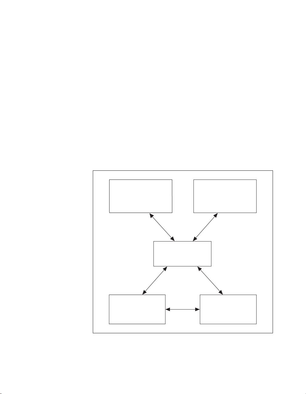
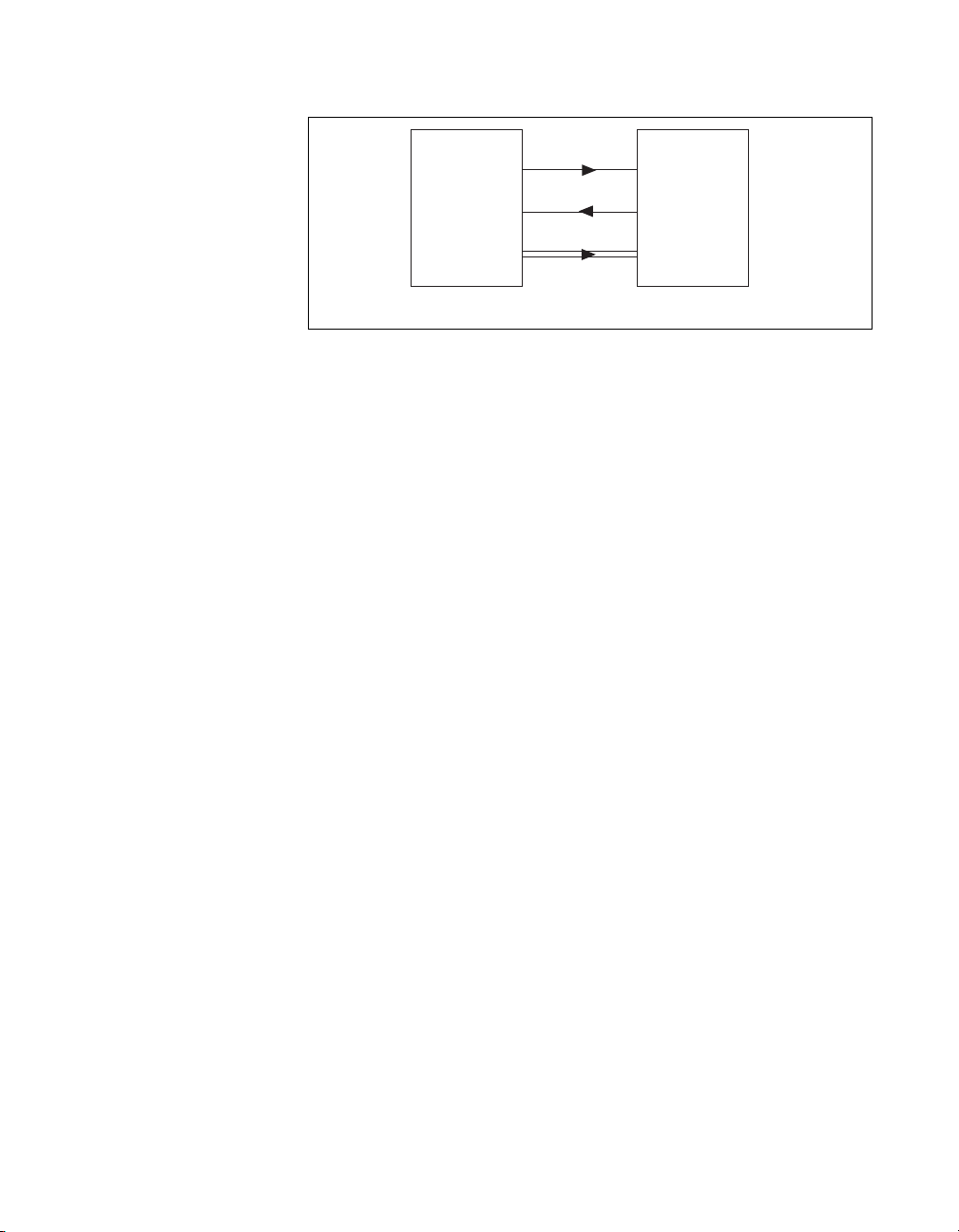
in Figure 1-1.
LabVIEW, LabVIEW RT,
Measurement Studio,
or Virtual Bench
DAQ or
SCXI Hardware
Figure 1-1.
The Relationship Between the Programming Environment,
Conventional
Programming Environment
NI-DAQ
Driver Software
Personal
Computer or
Workstation
NI-DAQ, and Your Hardware
653X User Manual 1-4 ni.com
Page 14

Chapter 1 Getting Started with Your 653X
To download a free copy of the most recent version of NI-DAQ, click
Download Software at
device using the following table:
ni.com
. Find NI-DAQ compatibility for your
NI-DAQ Version
Device Supported
PCI-DIO-32HS Version 5.0 or later Version 6.1.0 or later
AT-DIO-32HS Version 5.0 or later N/A
PXI-6533 Version 5.1 or later Version 6.1.3 or later
DAQCard-6533 for PCMCIA Version 5.1 or later Version 6.1.0 or later
PXI-6534 Version 6.9 or later N/A
PCI-6534 Version 6.9 or later N/A
PCI or PXI-7030/6533 Version 6.5.2 or later N/A
Windows Mac
Installing Your Software
Install application development software, such as LabVIEW or
Measurement Studio, according to instructions on the CD and the release
notes. If NI-DAQ was not installed with your ADE, then install NI-DAQ
according to the instructions on the CD and the DAQ Quick Start Guide
included with your device.
Note
It is important to install the NI-DAQ driver software before installing your device(s)
to ensure the device(s) are properly detected.
Unpacking Your 653X Device
Your 653X device is shipped in an antistatic package to prevent
electrostatic damage to the device. To avoid such damage in handling the
device, take the following precautions:
• Ground yourself via a grounding strap or by holding a grounded object.
• Touch the antistatic package to a metal part of your computer chassis
before removing the device from the package.
Caution
from damaging the device.
© National Instruments Corporation 1-5 653X User Manual
Never touch the exposed pins of connectors to prevent electrostatic discharge
Page 15

Chapter 1 Getting Started with Your 653X
Remove the device from the package and inspect the device for loose
components or any sign of damage. Notify National Instruments if the
device appears damaged in any way. Do not install a damaged device into
your computer.
Store your 653X device in the antistatic envelope when not in use.
Installing Your 653X Device
The following are general installation instructions. Consult your computer
or chassis user manual or technical reference manual for specific
instructions and warnings about installing new devices.
Note
It is important to install the NI-DAQ driver software before installing your device(s)
to ensure the device(s) are properly detected.
Installing the PCI-DIO-32HS, PCI-6534, or PCI-7030/6533
You can install a PCI-DIO-32HS, PCI-6534, or PCI-7030/6533 device in
any available 5 V PCI expansion slot in your computer.
1. Turn off and unplug your computer.
2. Remove the cover.
3. Remove the expansion slot cover on the back panel of the computer.
4. Touch a metal part of your computer chassis to discharge any static
electricity that might be on your clothes or body.
5. Insert the 653X device into a 5 V PCI slot. It can be a tight fit, but do
not force the device into place.
6. Screw the mounting bracket of the 653X device to the back panel rail
of the computer.
7. Visually verify the installation. Make sure the device is not touching
other boards or components and is inserted fully in the slot.
8. Replace the cover of your computer.
9. Plug in and turn on your computer.
Now that your 653X device is installed, it is ready to be configured.
653X User Manual 1-6 ni.com
Page 16

Chapter 1 Getting Started with Your 653X
Installing the PXI-6533, PXI-6534, or PXI-7030/6533
You can install a PXI-653X or PXI-7030/6533 device any available 5 V
peripheral slot in your PXI or CompactPCI chassis.
Note
Your PXI device has connections to several reserved lines on the CompactPCI J2
connector. Before installing a PXI device in a CompactPCI system that uses J2 connector
lines for purposes other than PXI, see Appendix C, Connecting Signals with Accessories.
1. Turn off and unplug your PXI or CompactPCI chassis.
2. Choose an unused PXI or CompactPCI 5 V peripheral slot.
Tip
For maximum performance of your CompactPCI, install the PXI-653X in a slot that
supports bus arbitration or bus-master cards. The PXI-653X contains onboard bus-master
DMA logic that can operate only in such a slot. If you install in a slot that does not support
bus masters, you must disable the PXI-653X onboard DMA controller using your software.
PXI-compliant chassis have bus arbitration for all slots.
3. Remove the filler panel for the peripheral slot you have chosen.
4. Touch a metal part on your chassis to discharge any static electricity
that might be on your clothes or body.
5. Insert the PXI-653X in a 5 V slot. Use the injector/ejector handle to
fully inject the device into place.
6. Screw the front panel of the PXI-653X to the front panel mounting rails
of the PXI or CompactPCI chassis.
7. Visually verify the installation. Make sure the device is not touching
other boards or components and is fully in the slot.
8. Plug in and turn on the PXI or CompactPCI chassis.
Now that your 653X device is installed, it is ready to be configured.
Installing the AT-DIO-32HS
You can install an AT-DIO-32HS in any available AT (16-bit ISA) or EISA
expansion slot in your computer.
1. Turn off and unplug your computer.
2. Remove the cover.
3. Remove the expansion slot cover on the back panel of the computer.
4. Touch a metal part of your computer chassis to discharge any static
electricity that might be on your clothes or body.
© National Instruments Corporation 1-7 653X User Manual
Page 17

Chapter 1 Getting Started with Your 653X
5. Insert the AT-DIO-32HS into an AT (16-bit ISA) or EISA slot. It can
be a tight fit, but do not force the device into place.
6. Screw the mounting bracket of the AT-DIO-32HS to the back panel rail
of the computer.
7. Visually verify the installation. Make sure the device is not touching
other boards or components and is fully inserted in the slot.
8. Replace the cover of the computer.
9. Plug in and turn on your computer.
Now that your 653X device is installed, it is ready to be configured.
Installing the DAQCard-6533 for PCMCIA
You can install your DAQCard-6533 for PCMCIA in any available
CardBus-compatible Type II PCMCIA slot. Consult the computer
manufacturer for information about slot compatibility.
1. Turn off your computer. If your computer and operating system
support hot insertion, you may insert or remove the DAQCard-6533
at any time, whether the computer is powered on or off.
2. Remove the PCMCIA slot cover on your computer, if any.
Now that your 653X device is installed, it is ready to be configured.
Configuring the 653
Your 653X device is configured automatically in Measurement &
Automation Explorer (MAX), which is installed with the NI-DAQ
driver software in Windows, or in the NI-DAQ Configuration Utility,
which is installed with NI-DAQ in the Mac OS. All settings are initially
configured to default settings.
X
In Windows
If you would like to change or view default settings, follow these
instructions, also available in your DAQ Quick Start Guide:
1. Launch MAX.
2. Open Devices and Interfaces.
3. Right-click the device you want to configure and choose Properties.
4. Press the Test Resources button to test hardware resources.
653X User Manual 1-8 ni.com
Page 18

In Mac OS
Chapter 1 Getting Started with Your 653X
To create a virtual channel, or to learn about other capabilities of MAX,
read the MAX online help by selecting Help»Help Topics and select
NI-DAQ from the menu.
To view and test current resource allocation:
1. Open the NI-DAQ Configuration Utility.
2. Select the device you want to configure.
3. Click the Configure button.
4. Press the Test Resources button to test hardware resources.
Warning
Do not configure the 653X resources in conflict with non-National Instruments
devices. For example, do not configure two devices to have the same base address.
Note
The PCI/PXI-7030/6533 configuration is similar to PCI/PXI-653X configuration
with a few exceptions. Refer to your PCI/PXI-7030
d LabVIEW RT User Manual for
an
specific configuration details.
Note
If you are using the AT-DIO-32HS device in a non-Plug and Play system, the device
automatically configures to a switchless DAQ device so it can work in the system.
Now that you have completed configuring your device, you can begin
setting up the device for use.
© National Instruments Corporation 1-9 653X User Manual
Page 19
Using Your 653X
To begin using your 653X device, navigate this chapter in the following
order:
1. Choose the correct mode of operation to perform using the table below.
2. Follow the instructions for the application you want to perform.
3. Refer to pinout diagrams in Appendix C, Connecting Signals with
Accessories, when you are ready to connect your devices and/or
accessories.
Tip
See the glossary for definitions to digital I/O terms used throughout this chapter.
Choosing the Correct Mode for Your Application
Use the following table to find the correct mode for your application:
Application Requirements Suggested Mode to Use
2
I need to perform basic digital I/O that does not need hardware timing or handshaking between
the 653X and the peripheral device.
I want to configure the direction of each bit individually instead of groups of eight. Unstrobed I/O
I want to connect two or more output drivers/pins to the same line. Unstrobed output with
I need to communicate with an external device using an exchange of signals to request and
acknowledge each data transfer.
I want to start and/or stop acquiring data upon a trigger and/or to transfer data at timed intervals. Pattern I/O
I want the 653X to capture input data only when certain lines change states. Change Detection
I want to monitor activity on input lines without continuously polling or transferring
unnecessary data during periods of inactivity.
© National Instruments Corporation 2-1 653X User Manual
Unstrobed I/O
wired-OR driver
Handshaking I/O–
Select appropriate
protocol
Change Detection
Page 20

Chapter 2 Using Your 653X
Controlling and Monitoring Static Digital Lines—Unstrobed I/O
This section explains how to control and monitor static digital lines through
software-timed reads and writes to and from the digital lines of your
653X device.
Configuring Digital Lines
For unstrobed I/O, the direction of each of the 32 data lines is individually
configurable. You can configure each data line to one of the following:
• Input
• Standard output
• Wired-OR output
Standard Output
A standard driver drives its output pin to approximately 0 V for logic low,
or +5 V for logic high. Advantages include:
• It does not require pull-up resistors.
• It is independent of the state of the DPULL line.
• It has high current drive for both its logic high and logic low states.
• It can drive high-speed transitions in both the high-to-low and
low-to-high directions.
Wired-OR Output
A wired-OR output driver drives its output pin to 0 V for logic low. For
logic high, the output driver assumes a high-impedance state and does not
drive a voltage. This is called tri-state. To pull the pin to +5 V for logic
high, a pull-up resistor is required.
To provide a pull-up resistor, connect the DPULL pin on the I/O connector
to the +5 V pin. This provides 100 kΩ pull-up resistors on all data lines.
For more information about CPULL and DPULL, see the Power-On State
section in Appendix D, Hardware Considerations.
653X User Manual 2-2 ni.com
Page 21

Advantages of using the wired-OR driver include:
• The ability to connect two or more wired-OR outputs together without
damaging the drivers.
• The ability to connect wired-OR outputs to open-collector drivers,
to GND signals, or to switches connecting to GND signals, without
damaging the drivers.
• The ability to use wired-OR outputs bidirectionally. If you connect
wired-OR outputs together, you can read back the value of a pin to
determine if any connected outputs are logic low.
Using Control Lines as Extra Unstrobed Data Lines
The 653X device has two timing controllers for high-speed data transfer
(Group 1 and Group 2). Each group contains four control lines which can
be used to time the input/output of data with hardware precision. You can
use Groups 1 and 2 to:
• Generate or receive digital patterns and waveforms at regular intervals
or timed by an external TTL signal.
• Transfer data between two devices using one of six configurable
handshaking protocols.
• Acquire digital data every time the state of a data line changes.
Chapter 2 Using Your 653X
Note
If you configure either group to perform handshaking I/O or pattern I/O, the
associated timing control lines for that group will not be available for unstrobed I/O.
If you are not using Group 1 and/or Group 2 as timing controllers to
perform pattern I/O or handshaking I/O, you can use their control lines as
extra data lines. These lines constitute Port 4. The direction and output
driver type of these lines are not configurable—four lines are used as input
only and four are used as standard output only. Even though there are eight
actual lines, the port width for Port 4 is 4 bits. In software, these lines are
collectively referred to as Port 4; when writing to Port 4, the output lines
are affected, and when reading from Port 4, the input lines are read.
Table 2-1 displays how Port 4 lines are organized.
© National Instruments Corporation 2-3 653X User Manual
Page 22
Chapter 2 Using Your 653X
Connecting Signals
Creating a Program
Table 2-1.
Direction Line I/O Pins
Input 0 STOPTRIG 1
Output (standard) 0 PCLK 1
Connect digital input signals to the I/O connector using the pinout
diagrams, Figures C-1, 653X I/O Connector 68-Pin Assignments,
and C-2, 68-to-50-Pin Adapter Pin Assignments.
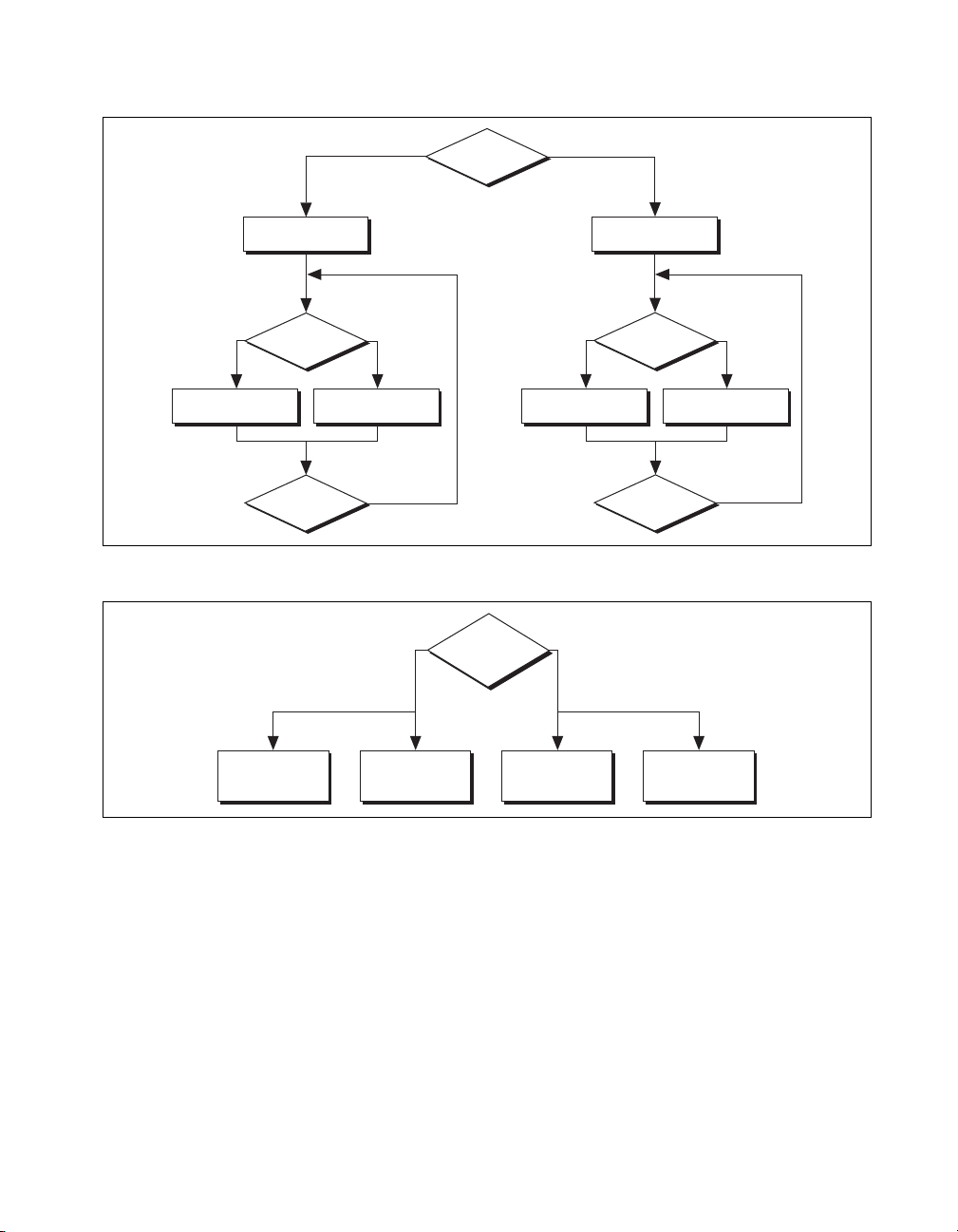
Using the following flowcharts as a guide, create a program to perform
unstrobed I/O. Figure 2-1 displays a flowchart for C programming using
NI-DAQ, while Figure 2-2 shows a LabVIEW programming flowchart.
Port 4 Lines
1 STOPTRIG 2
2 REQ 1
3 REQ 2
1 PCLK 2
2 ACK 1
3 ACK 2
The boxes represent function names for the appropriate software, and the
diamonds represent decision points.
653X User Manual 2-4 ni.com
Page 23
Chapter 2 Using Your 653X
Read?
Done?
No
Only One
Line?
NoYe s
DIG_Out_prtDIG_In_prt
No
Figure 2-1.
Ye s
DIG_Line_ConfigDIG_Prt_Config
Read?
Done?
NoYe s
DIG_Out_LineDIG_In_Line
No
Programming Unstrobed I/O in NI-DAQ
s
Ye s N o
Single Line?
Read from
Digital Line VI
Write to
Digital Line VI
Figure 2-2.
Programming Unstrobed I/O in LabVIEW/LabVIEW RT
Read from
Digital Port VI
Write to
Digital Port VI
Programming the Control/Timing Lines as Extra Unstrobed Data Lines
If you want to use the control/timing lines as extra unstrobed data lines:
• NI-DAQ C Interface—If both sets of control/timing lines are available,
call the
DIG_In_Prt
to 4. If both sets of control/timing lines are not available, use the
DIG_In_Line
and
read/write to the appropriate control/timing lines.
© National Instruments Corporation 2-5 653X User Manual
DIG_Out_Prt
or
DIG_Out_Line
function and set Port Number
functions to individually
Page 24
Chapter 2 Using Your 653X
• LabVIEW—Use one of the top-level VIs: the Read From Digital Line
VI to read from a digital port, and the Write to Digital Line VI to write
to a digital port. The digital channel number is 4 and the port width is
4. If one of the control/timing lines is used or reserved and you are
using the write or read port VIs, use the Line Mask parameter in the
DIO Port Write VI to mask out the appropriate lines.
Transferring Data Between Two
Devices—Handshaking I/O
If you want to communicate with an external device using an exchange of
signals to request and acknowledge each data transfer, use the handshaking
I/O mode.
Deciding the Width of Data to Transfer
You can choose between a width of eight, 16, or 32 bits. Use the following
table to find the valid combinations of ports and timing controllers you can
use based on the width of data you want to transfer.
Table 2-2.
Transfer
Width
8 bits Port 0 (DIOA<0..7>) Group 1
Port 2 (DIOC<0..7>) Group 2
16 bits Port 0, Port 1 Group 1
Port 2, Port 3 Group 2
32 bits Port 0, Port 1, Port 2, Port 3 Group 1
Deciding Data Transfer Direction
You can choose to send data from the 653X device to the peripheral device
(output) or from the peripheral device to the 653X device (input).
Port and Timing Controller Combinations
Possible Port
Combinations
Timing Controllers
That Can Be Used
653X User Manual 2-6 ni.com
Page 25

Deciding Which Handshaking Protocol to Use
The 653X device supports several different handshaking protocols to
communicate with your peripheral device. The protocol you select will
determine the timing of the ACK and REQ signals.
From the perspective of the 653X device, the peripheral device requests
the transfer of data by signaling on the REQ line. The 653X device
acknowledges it is ready to transfer data by signaling on the ACK line.
Use Table 3-1, Handshaking Protocol Characteristics, to select a
handshaking protocol for your application. To select a protocol compatible
with your peripheral device, compare the handshaking sequence and state
machine diagrams for each protocol in the later sections of Chapter 3,
Timing Diagrams.
Using the Burst Protocol
The burst protocol differs from all the other handshaking protocols in that
it is the only synchronous (clocked) protocol. In addition to ACK and REQ,
the 653X and peripheral device share a clock signal over the PCLK line.
See Chapter 3, Timing Diagrams, for more information about the burst
protocol.
Chapter 2 Using Your 653X
If you want to acquire or generate patterns of every edge of a clock
signal, see the Generating and Receiving Digital Patterns and
Waveforms—Pattern I/Osection.
Note
Feed external clocking signals into the PCLK pin for burst-mode handshaking and
into the REQ pin when performing pattern I/O.
Deciding the PCLK Signal Direction
The 653X device can receive an external PCLK signal to control data
transfers or generate a PCLK signal using an internal 32-bit counter to
output to the peripheral device. By default, the 653X device generates the
PCLK signal for input operations and receives an external PCLK signal for
output operations.
© National Instruments Corporation 2-7 653X User Manual
Page 26
Chapter 2 Using Your 653X
To set the direction of the PCLK signal:
• NI-DAQ C interface—Set the
in
Set_DAQ_Device_Info.
ND_CLOCK_REVERSE_MODE
• LabVIEW—Set the Clock Reverse Mode attribute to ON in the
DIO Parameter VI.
Note
For more information on LabVIEW VIs and NI-DAQ functions, consult the
LabVIEW Help and the NI-DAQ Function Reference Help.
Selecting ACK/REQ Signal Polarity
For all handshaking protocols except 8255 emulation, you can set the
polarity of the ACK and REQ signals to Active High or Active Low
through software. By default, these signals are active high in NI-DAQ
functions and active low in LabVIEW VIs. Refer to Table C-1, 653X I/O
Connector 68-Pin Assignments, for an overview of all control/timing
trigger lines.
Choosing Whether or Not to Use a Programmable Delay
For all the protocols, you have the option to set a programmable delay.
This is useful when the handshaking signals of the 653X device occur faster
than the peripheral device can handle.
to
ND_ON
For all protocols except burst, the delay increases the time the 653X device
takes to respond to the REQ signal. For the burst protocol, the
programmable delay selects the frequency of the clock signal when you are
using an internally generated clock source. You can change the PCLK
frequency by modifying the ACK Modify Amount parameter of the Digital
Mode Config VI or the ACK Delay Time attribute of the
DIG_Grp_Mode
function in NI-DAQ C interface. Use the following table to find the
resulting period in nanoseconds. The PCLK frequency is then selected by
the driver based on this choice.
PCLK Period in ns PCLK Frequency in MHz
50 20
100 10
200 5
300 3.33
400 2.5
653X User Manual 2-8 ni.com
Page 27

PCLK Period in ns PCLK Frequency in MHz
500 2
600 1.66
700 1.43
The state machine diagrams in Chapter 3, Timing Diagrams, show more
precisely where this delay occurs in the handshaking sequence.
Choosing Continuous or Finite Data Transfer
You can transfer data indefinitely to/from computer memory or finitely by
specifying the number of points you want to transfer.
Finite Transfers
For finite transfers, the 653X device transfers the specified amount of data
to/from a computer memory buffer and stops the operation.
Continuous Input
For continuous input, the 653X device transfers input data to the computer
memory buffer continuously. As the device is filling the buffer, call the
DIG_DB_Transfer
If at any time the device runs out of space in the buffer, it pauses the
handshaking operation until your program clears up more buffer space.
function or the DIO Read VI to retrieve the data.
Chapter 2 Using Your 653X
You have the option to allow the device to continue acquiring data when it
runs out of buffer space and overwrite data you have not yet read. You can
specify this through the oldDataStop parameter in the
function and the Data Overwrite/Regenerate parameter in the Digital
Buffer Control VI called by the DIO Start VI.
DIG_DB_Config
Continuous Output
Similarly, with continuous output, the 653X device continuously reads data
from computer memory. As the device retrieves data from the buffer, call
the
DIG_DB_Transfer
the buffer. The device will pause the handshaking operation if it runs out of
data to output. The data transfer will resume once more data is available.
© National Instruments Corporation 2-9 653X User Manual
function or the DIO Write VI to write new data to
Page 28

Chapter 2 Using Your 653X
You have the option to allow it to regenerate data that has already been
outputted. As in continuous input, you specify the device to allow
regeneration though the oldDataStop parameter in the
function and the Data Overwrite/Regenerate parameter in the Digital
Buffer Control VI, called by the DIO Start VI.
With 6534 devices, if you want to output the same block of data repeatedly,
you have the option of loading a buffer of data into on-board memory and
looping through this data block continuously. With this option, data is only
transferred from computer memory to the device on-board memory once,
and the device outputs the same block of data continuously from its
on-board memory. This allows the device to output data at higher rates
because it is not limited by the PCI bus bandwidth. To enable onboard
memory looping:
• NI-DAQ C interface—Set the
ND_PATTERN_GENERATION_LOOP_ENABLED
Set_DAQ_Device_Info
• LabVIEW—Set the Pattern Generation Loop Enable attribute to ON in
the DIO Parameter VI.
function.
DIG_DB_Config
to ND_ON in the
Choosing DMA or Interrupt Transfers
When using DMA (by default), the 6534 device transfers data in 32-byte
blocks and the 6533 device transfers data in 4-byte blocks. Therefore, at
any time during a continuous operation, there may be up to 31 bytes (or
3 bytes for 6533 devices) of data in an internal device FIFO. You can use
interrupt driven transfers if you need to retrieve data immediately as it is
acquired. Interrupt driven transfers are slower and take more processing
time from the computer than DMA driven transfers.
Connecting Signals
1. Connect the digital input signals to the I/O connector using the pinout
diagrams, Figure C-1, 653X I/O Connector 68-Pin Assignments,
and C-2, 68-to-50-Pin Adapter Pin Assignments.
2. Connect the ACK pin of the 653X device to the 653X-ready line of the
peripheral device.
3. Connect the REQ pin of the 653X device to the peripheral-ready line
of the peripheral device.
653X User Manual 2-10 ni.com
Page 29
Chapter 2 Using Your 653X
653X Device
If you are using the burst protocol, make the connection to the appropriate
PCLK pin on the 653X device.
Choosing the Startup Sequence
To avoid invalid or missing data when the ACK and REQ lines change
polarity to either active-high or active-low, start a transfer using one of the
following methods:
• Control the configuration and use an initialization order.
• Select compatible line polarities and default line levels.
Using an Initialization Order
This startup sequence ensures the 653X device is configured and is driving
a valid ACK value before you enable the transfer on the peripheral device.
Similarly, you can make sure the peripheral device is configured and is
driving a valid REQ value before you enable the transfer on the
653X device:
1. Configure the 653X device for a mode compatible with your peripheral
device.
2. Configure and reset the peripheral device, if appropriate.
3. Enable the input device (653X device or peripheral device) and begin
a transfer.
4. Enable the output device (653X device or peripheral device) and begin
a transfer.
ACK
REQ
I/O
Figure 2-3.
Confirm
Ready
I/O
Your Peripheral Device
Connecting Signals
To control this initialization order, you need to enable and disable the
peripheral device and control the order in which the 653X device and the
peripheral device are enabled. You can use the extra input and output lines
for this purpose.
© National Instruments Corporation 2-11 653X User Manual
Page 30

Chapter 2 Using Your 653X
Controlling the startup sequence does not apply to buffered (block)
operations. In a buffered operation, the NI-DAQ C interface configures and
enables the 653X device at the same time, when you start the actual data
transfer. For buffered operations, control the line polarities as a start-up
method.
Controlling Line Polarities
If you cannot control the initialization order of the 653X device and
peripheral device, you can ensure an optimum startup if you select the
polarities of the ACK and REQ lines so that the power-up, undriven states
of the control lines are the inactive states.
By default, the power-up, undriven control-line state of the REQ and ACK
lines is low. If you want to change state to high, use one of the three
following methods:
• Use the CPULL bias-selection line and connect the CPULL pin on the
I/O connector to the +5 V pin. This provides 2.2 kΩ pull-up resistors
on all control lines.
• Choose a mode with active-high REQ and ACK signals.
• Use your own pull-up resistors.
For information about using the CPULL line to control the pull-up and
pull-down resistors, see the Power-On State section in Appendix D,
Hardware Considerations.
Creating a Program
Using the following flowcharts as a guide, create a program to
perform handshaking I/O. Figures 2-4 and 2-5 display flowcharts for
C programming using NI-DAQ, while Figures 2-6 and 2-7 show a
LabVIEW programming flowcharts.
The boxes represent function names for the appropriate software, and the
diamonds represent decision points.
653X User Manual 2-12 ni.com
Page 31

DIG_Grp_Config
Chapter 2 Using Your 653X
DIG_Grp_Mode
Continuous?
No
Read?
No
Ye s
Ye s
Ye s
Read?
DIG_DB_Config
DIG_Block_In
DIG_Block_Out
Figure 2-4.
DIG_Block_In
No
DIG_Block_Out
DIG_Block_Check
DIG_DB_HalfReady
No
Acquisition
Complete?
Ye s
Programming Buffered Handshaking I/O in NI-DAQ
No
Is the
next half buffer
ready?
Ye s
DIG_DB_Transfer
No
Acquisition
Complete?
Ye s
DIG_Block_Clear
© National Instruments Corporation 2-13 653X User Manual
Page 32

Chapter 2 Using Your 653X
DIG_Grp_Config
DIG_Grp_Mode
Input?
Ye s
DIG_Grp_Status
Ready?
Ye s
DIG_In_Grp
DIG_In_Grp
Done?
Ye s
DIO_Grp_Config
No
No
No
DIG_Out_Grp
DIG_Grp_Status
Ready?
Ye s
Done?
Ye s
DIO_Grp_Config
No
No
*
*Clear Configuration
Figure 2-5. Programming Unbuffered Handshaking I/O in NI-DAQ
653X User Manual 2-14 ni.com
Page 33

Chapter 2 Using Your 653X
Buffered
Operation?
No
Digital Group
Config VI
Digital Single
Read VI
Digital Group
Config VI
Resets lines to
default states.
Ye s
DIO Parameter VI
DIO Config VI
Burst
Mode?
Ye s
Reverse
PCLK
Direction?
Ye s
No
No
DIO Start VI
Finite
Buffer?
Ye s
DIO Read VI
Reverse
PCLK
Direction?
No
DIO Clear VI
No
Ye s
Ye s
DIO Parameter VI
DIO Read VI
Done?
No
Figure 2-6.
Programming Handshaking Input in LabVIEW/LabVIEW RT
© National Instruments Corporation 2-15 653X User Manual
Page 34

Chapter 2 Using Your 653X
Buffered
Operation?
No
Digital Group
Config VI
Digital Single
Write VI
Digital Group
Config VI
Resets the lines
to default states.
Ye s
DIO Parameter VI
DIO Config VI
DIO Write VI
Burst
Mode?
Ye s
Reverse
PCLK
Direction?
Ye s
No
No
DIO Start VI
Finite
Buffer?
Ye s
DIO Wait VI
Reverse
PCLK
Direction?
No
No
Ye s
Ye s
DIO Parameter VI
DIO Write VI
Done?
No
DIO Clear VI
Figure 2-7. Programming Handshaking Output in LabVIEW/LabVIEW RT
By default, for output buffered transfers the 6534 device will preload the on
board memory with data before starting the output operation. This is done
to eliminate or reduce the impact of the PCI bus bandwidth limitations and
increase the overall transfer rate.
653X User Manual 2-16 ni.com
Page 35

Chapter 2 Using Your 653X
The preloading process will cause a small delay between the start command
in software and the actual start of data transfer. If this is a concern, you may
disable the preloading by calling the following function/VI before the
software start command:
• NI-DAQ C interface—In the
the ND_FIFO_Transfer_COUNT to ND_NONE.
• LabVIEW—In the DIO Parameter VI, set the Scarabs Preload Enable
attribute to OFF.
Set_DAQ_Device_Info
Generating and Receiving Digital Patterns and Waveforms—Pattern I/O
Using pattern I/O, you can acquire or generate patterns on every rising or
falling edge of a clock signal. The clock signal can be generated internally
by an onboard 32-bit counter set to a user-specified frequency or the clock
signal can be received from the REQ pin in the I/O connector.
Note
Feed external clocking signals into the PCLK pin for burst-mode handshaking and
into the REQ pin when performing pattern I/O.
function, set
Deciding the Width of Data to Transfer
You can choose between a width of eight, 16, or 32 bits. Use the following
table to find the valid combinations of ports and timing controllers you can
use based on the width of data you want to transfer.
Table 2-3.
Transfer
Width
8 bits Port 0 (DIOA<0..7>) Group 1
Port 2 (DIOC<0..7>) Group 2
16 bits Port 0, Port 1 Group 1
Port 2, Port 3 Group 2
32 bits Port 0, Port 1, Port 2, Port 3 Group 1
© National Instruments Corporation 2-17 653X User Manual
Port and Timing Controller Combinations
Possible Port
Combinations
Timing Controllers
That Can Be Used
Page 36

Chapter 2 Using Your 653X
Deciding Transfer Direction
You can choose to send data from your 653X device to the peripheral
device (output), or from the peripheral device to your 653X device (input).
Choosing an Internal or External REQ Source
In pattern I/O, the 653X device acquires/generates data on every falling or
rising edge (programmable) of the REQ signal. The REQ signal can be
generated internally or based on the clock of a peripheral device. An
example of using external REQ is sharing a sample clock of an analog input
device so you can synchronize the analog and digital operations.
Deciding the REQ Polarity
By default, data from an external REQ source is transferred on the rising
edge of the signal and on the falling edge of the internal REQ source. You
can reverse the REQ polarity by using the following functions:
• NI-DAQ C interface—Specify the REQ polarity in the
DIG_Group_Mode
DIG_Block_PG_Config
• LabVIEW—Specify the REQ polarity in the Digital Mode Config VI
that is called by the DIO Config VI.
function before calling the
function.
Note
For more information on LabVIEW VIs and NI-DAQ functions, consult the
LabVIEW Help and the NI-DAQ Function Reference Help.
Refer to Table C-1, 653X I/O Connector 68-Pin Assignments, for an
overview of all control/timing trigger lines.
Deciding the Transfer Rate
If you are generating the REQ signal internally, you need to specify the rate
of data transfer. The transfer rate is specified in software by using two
parameters, the timebase frequency and timebase divisor:
transfer rate (Hz)
where
timebase frequency = 20 MHz, 10 MHz, 1 MHz, 100 kHz, 10 kHz,
1 kHz, or 100 Hz, and
timebase divisor = an integer between 1 and 65,355.
653X User Manual 2-18 ni.com
timebase frequency
----------------------------------------------=
timebase divisor
Page 37

Chapter 2 Using Your 653X
For example, if you specify a timebase of 100 kHz and a timebase divisor
of 25, the resulting acquisition/generation rate would be 4 kHz.
100 kHz/25 = 4 kHz.
Note
If you are using a version of NI-DAQ prior to version 6.8, the minimum value for
timebase divisor is 2.
Note
In LabVIEW, you can specify the transfer rate directly using the Digital Clock
Config VI (called by the DIO Start VI). The software will choose the closest transfer rate
by selecting the frequency and divisor. To see the actual transfer rate, create an indicator at
the actual clock frequency output of the Digital Clock Config VI.
Deciding How to Start and Stop Data Transfer—Triggering
By default, data transfer starts upon a software command (the Digital
Buffer Control VI called by the DIO Start VI in LabVIEW and the
DIG_Block_In
and
DIG_Block_Out
However, you have the option of using a hardware trigger to start, stop, or
start and stop data transfer.
The three types of trigger signals available are the start trigger, the stop
trigger, or the start and stop trigger.
functions in NI-DAQ C interface).
Start Trigger
A start trigger is a trigger that initiates a pattern I/O upon receipt of a
hardware trigger on the ACK (STARTTRIG) pin.
ACK (STARTTRIG)
REQ
Posttrigger Data
Figure 2-8.
Starting Data Transfer Using a Trigger
Stop Trigger
When using a stop trigger, transfer starts upon a software command. Once
a hardware trigger is received on the STOPTRIG pin, a predetermined
amount of pretrigger and posttrigger data is saved in the buffer. Once this
© National Instruments Corporation 2-19 653X User Manual
Page 38

Chapter 2 Using Your 653X
data is in the buffer, transfer stops. If the stop trigger arrives before all the
pretrigger data is acquired, NI-DAQ returns an error.
STOPTRIG
REQ
Pretrigger Data
Figure 2-9. Stopping Data Transfer Using a Trigger
Posttrigger Data
Start and Stop Trigger
When using a start and stop trigger, transfer starts upon receiving a trigger
on the start trigger line (ACK/STARTTRIG pin) and ends upon receiving
a trigger on the stop trigger line (STOPTRIG pin) and a predetermined
amount of pretrigger and posttrigger data is saved in the buffer. If a stop
trigger is received before a start trigger, it is ignored. If the stop trigger
arrives before all the pretrigger data is acquired, NI-DAQ returns an error.
ACK (STARTTRIG)
STOPTRIG
REQ
Pretrigger Data Posttrigger Data
Figure 2-10. Using a Start and Stop Trigger
Pattern-Matching Trigger (Input Only)
Instead of using an external signal on the start/stop trigger pins on the
I/O connector, you may start or stop (not both) an operation once a
user-specified digital pattern is matched or not matched.
Specify four parameters to set up a pattern-matching trigger:
• Whether it is a start or stop trigger
• The data pattern to be detected/matched
• The mask, which selects the bits of interest for pattern comparison
(0 for bits not of interest)
653X User Manual 2-20 ni.com
Page 39

Chapter 2 Using Your 653X
• The polarity (whether to trigger on data that matches or mismatches
the specified pattern)
For example, if you want to start acquisition when the two least significant
bits of your data are 1 and 0, you would specify your trigger parameters to
match those in Figure 2-11.
Pattern to Detect
Mask
Polarity
Figure 2-11.
Tip To prevent a transient data value during line switching from falsely causing a match,
XXXXXX1 0
00000011
Pattern-Matching Trigger Example
set a valid pattern for at least 60 ns to guarantee detection. In addition, keep glitches to less
than 20 ns to guarantee rejection.
Choosing Continuous or Finite Data Transfer
You can transfer data continuously into or from computer memory or
specify the number of points you want to transfer.
Finite Transfers
For finite transfers, the 653X device transfers the specified amount of data
to/from computer memory and stops the operation.
Postive: Search for Match
Continuous Input
For continuous input, the 653X device transfers input data to the computer
memory buffer continuously. As the device is filling the buffer, call the
DIG_DB_Transfer
any time the device runs out of space in the buffer, it stops the operation
and NI-DAQ returns an error.
You have the option to allow the device to continue when it runs out of
buffer space and overwrite data you have not yet read. You can specify this
through the oldDataStop parameter in the
© National Instruments Corporation 2-21 653X User Manual
function or the DIO Read VI to retrieve the data. If at
DIG_DB_Config
function and
Page 40

Chapter 2 Using Your 653X
the Data Overwrite/Regenerate parameter in the Digital Buffer Control VI,
called by the DIO Start VI.
Continuous Output
Similarly, with continuous output, the 653X device continuously reads
data from computer memory. As the device retrieves data from the buffer,
call the
The device will stop and return an error if it runs out of data to output, but
you have the option to allow it to regenerate data that has already been
outputted. As in continuous input, you specify the device to allow
regeneration with the oldDataStop parameter in the
function and the data overwrite/regenerate parameter in the Digital Buffer
Control VI, called by the DIO Start VI.
With 6534 devices, if you want to output the same block of data repeatedly,
you have the option of loading a buffer of data into onboard memory and
looping through this data block continuously. With this option, data is only
transferred from computer memory to the device onboard memory once,
and the device outputs the same block of data continuously from its
onboard memory. This allows the device to output data at higher rates
because it is not limited by the PCI bus bandwidth. To enable on-oard
memory looping:
• NI-DAQ C interface—Set the
• LabVIEW—Set the Pattern Generation Loop Enable attribute to ON
DIG_DB_Transfer
ND_PATTERN_GENERATION_LOOP_ENABLED
Set_DAQ_Device_Info
in the DIO Parameter VI.
function or the DIO Write VI to write the data.
DIG_DB_Config
to ND_ON in the
function.
Choosing DMA or Interrupt Transfers
When using DMA (by default), the 6534 device transfers data in 32-byte
blocks and the 6533 device transfers data in 4-byte blocks. Therefore, at
any time during a continuous operation, there may be up to 31 bytes (or
3 bytes for 6533 devices) of data in an internal device FIFO. You can use
interrupt driven transfers if you need to retrieve data immediately as it is
acquired. Interrupt driven transfers are slower and take more processing
time from the computer than DMA driven transfers.
653X User Manual 2-22 ni.com
Page 41

Monitoring Data Transfer
To monitor your data transfer once data transfer starts:
• NI-DAQ C interface—Call
transfer. For continuous transfers, use
obtain the cumulative transfer count (
return the number of buffer iterations completed). The following table
lists the attribute types and values returned for
Get_DAQ_Device_Info
Transfer
Direction
Attribute Value Returned
DIG_Block_Check
Get_DAQ_Device_Info
DIG_Block_Check
:
Chapter 2 Using Your 653X
to monitor finite data
to
does not
Input
Output
ND_READ_MARK_H_SNAPSHOT_GR1
ND_READ_MARK_H_SNAPSHOT_GR1
ND_READ_MARK_L_SNAPSHOT_GR1
ND_READ_MARK_L_SNAPSHOT_GR2
ND_WRITE_MARK_H_SNAPSHOT_GR1
ND_WRITE_MARK_H_SNAPSHOT_GR2
ND_WRITE_MARK_L_SNAPSHOT_GR1
ND_WRITE_MARK_L_SNAPSHOT_GR2
Note
You should always read the least significant bits of the transfer count before reading
the most significant bits. The 32 most significant bits of the transfer count is cached in
software when you read the least significant bits.
Connecting Signals
Most significant 32-bit of transfer count
Least significant 32-bit of transfer count
Most significant 32-bit of transfer count
Least significant 32-bit of transfer count
• LabVIEW—Use the Digital Buffer Write VI or the Digital Buffer
Read VI, which are called by the DIO Read VI, the DIO Write VI, and
the DIO Wait VI.
Connect digital input signals to the I/O connector using the pinout
diagrams, Figures C-1, 653X I/O Connector 68-Pin Assignments, or C-2,
68-to-50-Pin Adapter Pin Assignments.
If you are using an external source for your REQ signal, connect it to the
appropriate REQ pin of the I/O connector.
© National Instruments Corporation 2-23 653X User Manual
Page 42

Chapter 2 Using Your 653X
Creating a Program
If you are using external start and/or stop triggers, connect to the
appropriate pins—start trigger (ACK/STARTTRIG) and/or stop trigger
(STOPTRIG).
Using the following flowcharts as a guide, create a program to perform
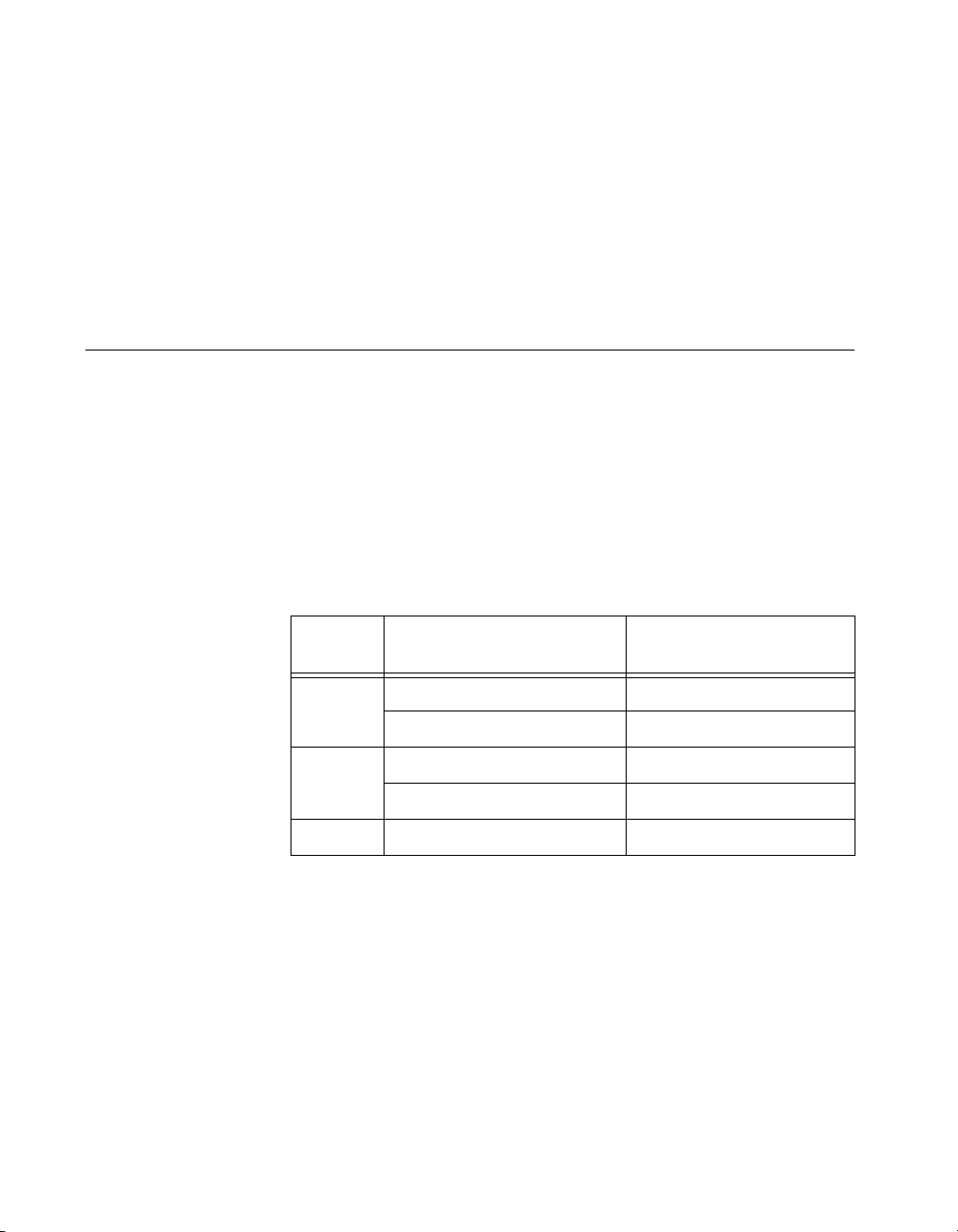
pattern I/O. Figures 2-13 and 2-14 display flowcharts for C programming
using NI-DAQ, while Figure 2-14 shows a LabVIEW programming
flowchart.
The boxes represent function names for the appropriate software, and the
diamonds represent decision points.
DIG_Block_Clear
DIG_Grp_Config
DIG_Block_PG_Config
Trigger?
Ye s
DIG_Trigger_Config
Ye s
Acquisition
Complete?
No
DIG_Block_In
Read?
Figure 2-12.
Ye s
No
DIG_Block_Out
Programming Pattern I/O (Single Buffer) in NI-DAQ
DIG_Block_Check
No
653X User Manual 2-24 ni.com
Page 43

Chapter 2 Using Your 653X
DIG_Grp_Config
DIG_Block_PG_Config
Trigger?
Ye s
DIG_Trigger_Config
DIO Config VI
Write?
Ye s
DIO Write VI
DIG_Block_In
Ye s
Read?
No
DIG_Block_Out
No
DIG_DB_Config
Figure 2-13.
Programming Pattern I/O (Continuous) in NI-DAQ
DIG_DB_HalfReady
No
No
Is the
next half buffer
ready?
Ye s
DIG_DB_Transfer
Acquisition
Complete?
Ye s
DIG_Block_Clear
DIO Clear VI
No
Digital Trigger Config VI
Trigger?
Ye s
No
Ye s
No
Trigger?
Ye s
Done?
No
Digital Trigger Config VI
DIO Read/Write VI
DIO Start VI
Figure 2-14.
Programming Pattern I/O in LabVIEW/LabVIEW RT
© National Instruments Corporation 2-25 653X User Manual
Page 44
Chapter 2 Using Your 653X
Note
If you are performing a finite pattern output operation, you can call the DIO Wait VI
instead of the DIO Write VI after the DIO Start VI. For more information about these VIs,
see the LabVIEW Help.
By default, for output buffered transfers the 6534 device will preload the on
board memory with data before starting the output operation. This is done
to eliminate or reduce the impact of the PCI bus bandwidth limitations and
increase the overall transfer rate. The preloading process will cause a small
delay between the start command in software and the actual start of data
transfer. If this is a concern, you may disable the preloading by calling the
following function/VI before the software start command:
• NI-DAQ C interface—In the
set the ND_FIFO_TRANSFER_COUNT to ND_NONE.
• LabVIEW—In the DIO Parameter VI, set the Scarabs Preload Enable
attribute to OFF.
Set_DAQ_Device_Info
Monitoring Line State—Change Detection
You can configure your 653X device to acquire data whenever the state of
one or more data lines change. Once the 653X device detects a change in
one of the selected lines, it will capture data within 50–150 ns and outputs
a pulse on the REQ pin. This mode increases CPU and bus efficiency
because you can monitor activity on input lines without continuously
polling or transferring unnecessary data during periods of inactivity.
function,
Tip
The 653X device used alone will detect if a change occurred, but if used in
conjunction with a 660X device (via a RTSI line), the relative time between changes can be
acquired by the 660X device.
Deciding the Width of Data to Acquire
You can choose between a width of eight, 16, or 32 bits. Use the following
table to find the valid combinations of ports and timing controllers you can
use based on the width of data you want to acquire.
Table 2-4. Port and Timing Controller Combinations
Transfer
Width
8 bits Port 0 (DIOA<0..7>) Group 1
Port 2 (DIOC<0..7>) Group 2
653X User Manual 2-26 ni.com
Possible Port
Combinations
Timing Controllers
That Can Be Used
Page 45

Chapter 2 Using Your 653X
Table 2-4.
Transfer
Width
Port and Timing Controller Combinations (Continued)
Possible Port
Combinations
16 bits Port 0, Port 1 Group 1
Port 2, Port 3 Group 2
32 bits Port 0, Port 1, Port 2, Port 3 Group 1
Deciding Which Lines You Want to Monitor
You need to specify which of the lines in your acquisition you want to
monitor for changes.
Specify which bits are significant to you by using a software line mask in
the
DIG_Trigger_Config
Digital Trigger Config VI for LabVIEW. In the following example, the user
specifies the mask to detect changes on the two least-significant bits of a
port. Pattern 1 does not have changes in the two bits of interest and data is
not latched, but for pattern 2, a change is detected on one of the two bits of
interest, and the value of the entire port is acquired.
Mask 00000011
function in NI-DAQ C interface, and the
Timing Controllers
That Can Be Used
Initial Input
00000010
Patter n
Input Pattern 1 01000010
Input Pattern 2 00000011
Figure 2-15.
Change Detection Example Settings
No change on specified
bits.
Data is not latched.
Change detected,
latch entire port.
Deciding How to Start and Stop Data Transfer—Triggering
By default, data transfer starts upon a software command (the
Digital Buffer Control VI called by the DIO Start VI in LabVIEW and the
DIG_Block_In
and
DIG_Block_Out
However, you have the option of using a hardware trigger to start, stop, or
start and stop data transfer.
© National Instruments Corporation 2-27 653X User Manual
functions in NI-DAQ C interface).
Page 46

Chapter 2 Using Your 653X
The three types of trigger signals available are the start trigger, the stop
trigger, or the start and stop trigger.
Start Trigger
A start trigger is a trigger that initiates a pattern I/O upon receipt of a
hardware trigger on the ACK (STARTTRIG) pin.
ACK (STARTTRIG)
REQ
Posttrigger Data
Figure 2-16.
Starting Data Transfer Using a Trigger
Stop Trigger
When using a stop trigger, transfer starts upon a software command. Once
a hardware trigger is received on the STOPTRIG pin, a predetermined
amount of pretrigger and posttrigger data is saved in the buffer. Once this
data is in the buffer, transfer stops. If the stop trigger arrives before all the
pretrigger data is acquired an error will return in software.
STOPTRIG
REQ
Pretrigger Data
Figure 2-17.
Stopping Data Transfer Using a Trigger
Posttrigger Data
Start and Stop Trigger
When using a start and stop trigger, transfer starts upon receiving a trigger
on the start trigger line (ACK/STARTTRIG pin) and ends upon receiving
a trigger on the stop trigger line (STOPTRIG pin) and a predetermined
amount of pretrigger and posttrigger data is saved in the buffer. If a stop
trigger is received before a start trigger, it is ignored. If the stop trigger
arrives before all the pretrigger data is acquired an error will return in
software.
653X User Manual 2-28 ni.com
Page 47

ACK (STARTTRIG)
STOPTRIG
REQ
Chapter 2 Using Your 653X
Pretrigger Data Posttrigger Data
Figure 2-18.
Using a Start and Stop Trigger
Pattern-Matching Trigger
Instead of using an external signal on the start/stop trigger pins on the
I/O connector, you may start or stop (not both) an operation once a
user-specified digital pattern is matched.
Specify four parameters to set a pattern-matching trigger:
• Whether it is a start or stop trigger
• The data pattern to be detected/matched
• The mask, which selects the bits of interest for pattern detection
Note
The mask for the pattern-matching trigger is the same as the one used for change
detection. In other words, input lines significant for the pattern-matching trigger are also
significant for change detection.
• Polarity (whether to detect data that matches or mismatches the
specified pattern)
The 653X device detects any occurrence of a specific pattern immediately
as the data comes in. When a match occurs, the 653X device starts
acquiring data. For example, if you want to start an acquisition when the
two least significant bits of your data are 1 and 0, you would specify your
trigger parameters to match those in Figure 2-19.
© National Instruments Corporation 2-29 653X User Manual
Page 48
Chapter 2 Using Your 653X
Value to Detect
Pattern
Mask
Polarity
Figure 2-19. Pattern-Detection Trigger Example
Tip
To prevent a transient data value during line switching from falsely causing a match,
XXXXXX1 0
00000010
00000011
set a valid pattern for at least 60 ns to guarantee detection. In addition, keep glitches to less
than 20 ns to guarantee rejection.
Choosing Continuous or Finite Data Transfer
You can acquire data continuously into or from computer memory or
specify the number of points you want to transfer.
Finite Transfers
For finite transfers, the 653X device inputs the specified amount of data to
a computer memory buffer and stops the operation.
Postive: Search for Match
Continuous Input
For continuous input, the 653X device transfers input data to the computer
memory buffer continuously. As the device is filling the buffer, call the
DIG_DB_Transfer
any time the device runs out of space in the buffer, it stops the operation
and NI-DAQ returns an error.
You have the option to allow the device to continue when it runs out of
buffer space and overwrite data you have not yet read. You can specify this
through the oldDataStop parameter in the
the Data Overwrite/Regenerate parameter in the Digital Buffer Control VI,
called by the DIO Start VI.
653X User Manual 2-30 ni.com
function or the DIO Read VI to retrieve the data. If at
DIG_DB_Config
function and
Page 49

Connecting Signals
Creating a Program
Chapter 2 Using Your 653X
Choosing DMA or Interrupt Transfers
When using DMA (by default), the 6534 device transfers data in 32-byte
blocks and the 6533 device transfers data in 4 byte blocks. Therefore, at any
time during a continuous operation, there may be up to 31 bytes (or 3 bytes
for 6533 devices) of data in an internal device FIFO. You can use interrupt
driven transfers if you need to retrieve data immediately as it is acquired.
Interrupt driven transfers are slower and take more processing time from
the computer than DMA driven transfers.
Connect digital input signals to the I/O connector using the pinout
diagrams, Figures C-1, 653X I/O Connector 68-Pin Assignments, or C-2,
68-to-50-Pin Adapter Pin Assignments.
If you are using external start and/or stop triggers, connect to the
appropriate pins—start trigger (ACK or STARTTRIG) and/or stop trigger
(STOPTRIG).
Using the following flowcharts as a guide, create a program to perform
change detection. Figure 2-21 and 2-22 display flowcharts for C
programming using NI-DAQ, while Figure 2-22 shows a LabVIEW
programming flowchart.
The boxes represent function names for the appropriate software, and the
diamonds represent decision points.
© National Instruments Corporation 2-31 653X User Manual
Page 50
Chapter 2 Using Your 653X
DIG_Grp_Config
DIG_Block_In
DIG_Block_PG_Config
DIG_Trigger_Config DIG_DB_Config
Specify data mask here
Figure 2-20. Programming Change Detection (Continuous) in NI-DAQ
DIG_Grp_Config
DIG_Block_PG_Config
DIG_DB_HalfReady
No
Is the
next half buffer
ready?
Ye s
DIG_DB_Transfer
No
Acquisition
Complete?
Ye s
DIG_Block_Clear
DIG_Block_Clear
Ye s
DIG_Trigger_Config
DIG_Block_In
DIG_Block_Check
Acquisition
Complete?
No
Specify data mask here
Figure 2-21. Programming Change Detection (Single Buffer) in NI-DAQ
653X User Manual 2-32 ni.com
Page 51

DIO Config VI
Trigger Config VI
DIO Start VI
DIO Read VI
Chapter 2 Using Your 653X
Specify data mask here
Figure 2-22.
Done?
No
Ye s
DIO Clear VI
Programming Change Detection for LabVIEW/LabVIEW RT
© National Instruments Corporation 2-33 653X User Manual
Page 52

Timing Diagrams
This chapter contains timing diagrams for the handshaking and pattern I/O
modes. You can use these diagrams to get a detailed understanding about
what happens in hardware when using these modes.
Note
All timing diagrams are in nanoseconds.
Pattern I/O Timing Diagrams
Use pattern I/O to transfer data at a timed interval upon the rising or falling
edge of the REQ signal. The REQ signal can be generated internally by the
653X device or supplied externally via the I/O connector.
Note
Your transfer rate is limited by the minimum available bus bandwidth in your
computer system, unless you are using the PCI/PXI-6534 device, which has onboard
memory. Otherwise, you are limited by the number of other devices utilizing the bus and
your application software, both of which can lower your transfer rate. For more
information about transfer rates, see Appendix E, Optimizing Your Transfer Rates.
3
Internal REQ Signal Source
The 653X can internally generate a signal (REQ) with which to strobe data.
To program the frequency of this signal, specify the timebase and interval
as shown in the Deciding the Transfer Rate section of Chapter 2, Using
Your 653X. The device captures data on the rising (active low) or falling
edge (active high) of this signal. You can select the polarity of the REQ
signal through software, as described in the Deciding the REQ Polarity
section in Chapter 2, Using Your 653X.
When generating an internal REQ signal, the asserted time of the resulting
clock will be one period of the timebase used to generate the REQ. The
exception is if you use a 20 MHz timebase (50 ns) and select an interval
of 1. The REQ pulse is then asserted for 20–30 ns.
Note
If you are using a version of NI-DAQ prior to version 6.8, the minimum value for
the interval parameter is 2.
© National Instruments Corporation 3-1 653X User Manual
Page 53

Chapter 3 Timing Diagrams
Programmable = Interval x Timebase
dtp will remove bar
REQ if Active High
REQ if Active Low
Data Valid
(Output Mode)
Data Valid
(Input Mode)
t
c
Programmable = One Timebase
t
w
t
p
30 ns
Max
t
t
su
Min
h
0ns
Min
30 ns
Parameter Description
*
t
c
*
t
w
t
p
t
su
t
h
* The 6534 devices will transfer data at 20 MHz when the cycle time (tc) for REQ pulse is 50 ns and width of the REQ
pulse (t
) is 20–30 ns.
w
Cycle time
Width of pulse
Propagation time to valid output data
Setup time
Hold time
Figure 3-1. Internal Request Timing Diagram
External REQ Signal Source
Use an external request when you want to time data transfers using an
external signal on the REQ pin of the I/O connector. You can select the
polarity of the REQ signal. If active high (default), the 653X device will
latch the data on the I/O pins on the rising edge of the REQ signal. If active
low, the 653X device will latch the data on the I/O pins on the falling edge
of the REQ signal. The low time and high time of the REQ signal must each
be >20 ns. The minimum duration for a period of the REQ signal is 50 ns.
Note
For data transfers that use a hardware start trigger, there is no mandatory setup (tsu)
or hold time (t
653X User Manual 3-2 ni.com
) for the STARTRIG (ACK) signal. It can be asserted at any point before,
h
Page 54

Chapter 3 Timing Diagrams
during, or after the REQ edge. If STARTRIG is asserted too close to the REQ edge, it may
not be recognized until the next REQ edge. To avoid this uncertainty, you can observe an
optional setup time of 15 ns, in other words, assert STARTRIG at least 15 ns before the
start of the REQ pulse.
The STARTRIG signal is synchronized to the REQ edge using a flip-flop.
Because of this synchronization flip-flop, there is a one REQ-pulse delay
after STARTRIG before the data capture begins. There is a possibility of a
two-cycle delay if you do not observe the optional setup time mentioned in
the previous note.
t
c
50 ns Min
REQ
Data Valid
(Output Mode)
t
hw
20 ns Min
t
30 ns Max
p
t
w
20 ns Min
Data Valid
(Input Mode)
t
su
10 ns
Min
t
h
20 ns
Min
Parameter Description
t
c
t
hw
t
p
t
su
t
h
© National Instruments Corporation 3-3 653X User Manual
Cycle time
Width of low pulse
Propagation time to valid output data
Setup time
Hold time
Figure 3-2.
External Request Timing Diagram
Page 55

Chapter 3 Timing Diagrams
Handshaking I/O Timing Diagrams
This section compares of the handshaking I/O protocols and includes
timing diagrams for each:
• Handshaking sequence for input operation
• State machine for input operation
• Timing specification for input operation
• Handshaking sequence for output operation
• State machine for output operation
• Timing specification for output operation
Comparing the Different Handshaking Protocols
For an overview of all handshaking protocols supported by your
653X device, see Table 3-1.
Note
Whether an ACK or a REQ signal occurs first in the handshaking sequence depends
on the protocol and the direction of the transfer.
Table 3-1.
REQ/ACK
Protocol
Asynchronous Protocols
8255
Emulation
Level ACK Programmable Leading Before ACK
Leading-Edge Programmable Leading Before ACK
Long Pulse Programmable Leading Pulse width and
Trailing-Edge Programmable Trailing Pulse width and
653X User Manual 3-4 ni.com
Polarity
Active-low Trailing Between transfers Long Pulse
Handshaking Protocol Characteristics
Where the
Which REQ Edge
Requests Transfer
Programmable
Delay Is Located
and between transfers
and between transfers
between transfers
between transfers
Complementary Protocol(s)
Level ACK
Leading Edge
Long Pulse, 8255 Emulation,
and 8255
Trailing-Edge
Page 56

Chapter 3 Timing Diagrams
Table 3-1.
REQ/ACK
Protocol
Synchronous Protocol
Burst Programmable Neither (level REQ) Clock speed Burst
* Asynchronous protocols can compensate automatically to cable length, yet for synchronous protocols, you need to select
an appropriate speed for your cable when configuring your device.
Select a delay of at least the following:
• 0 for a typical cable up to 1 m
• 1 (70 ns) for a typical cable up to 5 m
• 2 (140 ns) for a typical cable up to 15 m long
Polarity
Handshaking Protocol Characteristics (Continued)
Where the
Which REQ Edge
Requests Transfer
Programmable
Delay Is Located
Complementary Protocol(s)
In order for the 653X device to communicate with peripheral devices in
handshaking mode, it is important to verify that:
• You are using complementary protocols. For example, use
8255-emulation protocol with long-pulse protocol.
• The ACK/REQ polarity are the same. For example, 8255 emulation
is active low only, so the other device must use the long-pulse protocol
and have active low ACK/REQ polarity.
Using the Burst Protocol
Burst protocol is a synchronous, or clocked, protocol. In addition to using
the ACK and REQ signals like the other handshaking protocols, in burst
protocol, the 653X device and the peripheral device share a clock signal
over the PCLK line.
The 653X device asserts the ACK signal if it is ready to perform a transfer.
If the peripheral device also asserts the REQ signal indicating it is ready,
a transfer occurs on the rising edge of the PCLK signal. See Figures 3-3
and 3-4 for examples of burst protocol transfers. Dashed lines indicate
when data is transferred.
© National Instruments Corporation 3-5 653X User Manual
Page 57

Chapter 3 Timing Diagrams
PCLK
ACK
REQ
Data In
Valid
PCLK
ACK
REQ
Data Out
Valid
D1
D2 D3 D4
D5
= data transfer occurs
Figure 3-3. Burst Transfer Example (Input)
D1
D2
D3 D4 D5
= data transfer occurs
Figure 3-4. Burst Transfer Example (Output)
Since data is transferred only when both the 653X device and the peripheral device
Note
are ready (and thus ACK and REQ are asserted), it is not reasonable to expect data to arrive
at consistent intervals. If consistent intervals are an important criteria for your application,
use pattern I/O.
653X User Manual 3-6 ni.com
Page 58

Chapter 3 Timing Diagrams
The 653X device can either drive an output clock signal onto the PCLK line
or receive an input clock signal from the PCLK line. By default, the PCLK
line is set for input during output transfers, and set for output during input
transfers.
Tip
If you are using long cables, slow down the PCLK clock signal to compensate for the
decrease in data setup time.
© National Instruments Corporation 3-7 653X User Manual
Page 59

Chapter 3 Timing Diagrams
PCLK
t
pc
t
pw
t
ah
t
rh
t
dih
ACK
REQ
Data In Valid
t
pa
t
rs
t
dis
Parameter Description Minimum Maximum
Input Parameters
t
rs
t
rh
t
dis
t
dih
Setup time from REQ valid to PCLK 12 —
Hold time from PCLK to REQ invalid 0 —
Setup time from input data valid to PCLK 4 —
Hold time from PCLK to input data invalid 6 —
Output Parameters
/2 + 5
pc
1
t
pc
t
pw
t
pa
t
ah
1
tpc = programmable delay from 100 to 700 ns, or 50 ns if programmable delay is 0. Timebase stability for the onboard
20 MHz clock source is 100 ppm.
All timing values are in nanoseconds.
PCLK cycle time 50 700
PCLK high pulse duration tpc/2 – 5t
PCLK to ACK valid — 18
Hold time from PCLK to ACK invalid 3 —
Figure 3-5. Burst Input Timing Diagram (Default)
653X User Manual 3-8 ni.com
Page 60

PCLK
Chapter 3 Timing Diagrams
t
pc
t
pw
t
pl
t
ah
t
rh
t
doh
ACK
REQ
Data Out Valid
t
pa
t
rs
t
pdo
Parameter Description Minimum Maximum
Input Parameters
t
pc
t
pw
t
pl
t
rs
PCLK cycle time 50 —
PCLK high pulse duration 20 —
PCLK low pulse duration 20 —
Setup time from REQ valid to PCLK
1—
falling edge
t
rh
Hold time from PCLK to REQ invalid 0 —
Output Parameters
t
pa
t
ah
t
pdo
t
doh
PCLK to ACK valid — 22
Hold time from PCLK to ACK invalid 3 —
PCLK to output data valid — 28
Hold time from PCLK to output data
5—
invalid
All timing values are in nanoseconds.
Figure 3-6. Burst Output Timing Diagram (Default)
© National Instruments Corporation 3-9 653X User Manual
Page 61

Chapter 3 Timing Diagrams
PCLK
t
pc
t
pw
t
pl
t
ah
t
rh
t
dih
ACK
REQ
Data In Valid
t
pa
t
rs
t
dis
Parameter Description Minimum Maximum
Input Parameters
t
pc
t
pw
t
pl
t
rs
PCLK cycle time
PCLK high pulse duration
PCLK low pulse duration
Setup time from REQ valid to PCLK falling
50 —
20 —
20 —
1 —
edge
t
rh
t
dis
Hold time from PCLK to REQ invalid
Setup time from input data valid to PCLK
0 —
0 —
falling edge
t
dih
Hold time from PCLK to input data valid
0 —
Output Parameters
t
pa
t
ah
All timing values are in nanoseconds.
PCLK to ACK valid
Hold time from PCLK to ACK invalid
— 22
3 —
Figure 3-7. Burst Input Timing Diagram (PCLK Reversed)
653X User Manual 3-10 ni.com
Page 62

PCLK
Chapter 3 Timing Diagrams
t
pc
t
pw
t
ah
t
rh
t
doh
ACK
REQ
Data Out Valid
t
pa
t
rs
t
pdo
Parameter Description Minimum Maximum
Input Parameters
t
rs
t
rh
Setup time from REQ valid to PCLK 12 —
Hold time from PCLK to REQ invalid 0 —
Output Parameters
/2 + 5
pc
1
t
pc
t
pw
t
pa
t
ah
t
pdo
t
doh
PCLK cycle time 50 700
PCLK high pulse duration tpc/2 – 5t
PCLK to ACK valid — 18
Hold time from PCLK to ACK invalid 3 —
PCLK to output data valid — 28
Hold time from PCLK to output data
4 —
invalid
t
dis
t
dih
1
tpc = programmable delay from 100 to 700 ns, or 50 ns if programmable delay is 0. Timebase stability for the board
20 MHz clock source is 50 ppm.
All timing values are in nanoseconds.
Setup time from input data valid to PCLK 0 —
Hold time from PCLK to input data invalid 0 —
Figure 3-8.
© National Instruments Corporation 3-11 653X User Manual
Burst Output Timing Diagram (PCLK Reversed)
Page 63

Chapter 3 Timing Diagrams
Using Asynchronous Protocols
All handshaking protocols except burst are asychronous. The asynchronous
protocols include 8255 emulation, level ACK, leading edge, trailing edge,
and long pulse.
When using these protocols, you have the following options:
• You can change the polarity of the ACK and REQ signals (except for
8255-emulation). The diagrams in this chapter show active-high
signals.
• You can set a programmable delay, from 0 to 700 ns, programmable in
increments of 100 ns. Use the programmable delay to insert wait states
if you have a slow peripheral device. A delay increases the duration of
each transfer. The location of the delay in the handshaking sequence
differs from protocol to protocol. In addition, a delay increases the
minimum spacing between consecutive transfers.
• You can enable request-edge latching, where in input, the 653X device
latches data in from the I/O connector on the active REQ edge before
reading the data. For output, after writing the data, the 653X device
latches data out of the I/O connector on the active REQ edge. The
active edge of the REQ is determined (rising or falling) by the
handshaking protocol and the REQ polarity.
Using the 8255-Emulation Protocol
Your 653X device can perform handshaking I/O with devices that contain
the 8255 chip, including National Instruments PC-DIO-24/PnP,
650X family, and PC-DIO-96/PnP. Performing the 8255-emulation
protocol with your 653X device is similar to 8255 or 82C55 Programmable
Peripheral Interface (PPI).
Note
The 653X devices does not emulate the bidirectional protocol of a 8255 device.
The 653X device can perform back-to-back transfers much faster than a
true 8255-based device. If your peripheral device requires more time
between transfers, configure the 653X device to add a data-settling delay
between transfers.
Note
In the 8255-emulation protocol, ACK and REQ are active low, reflected in the
following timing diagrams. For all other handshaking I/O protocols, the polarity of the
ACK and REQ are programmable, but are shown as active high signals in the following
diagrams.
653X User Manual 3-12 ni.com
Page 64
Chapter 3 Timing Diagrams
653X device terminology differs from 8255 terminology.
• Input—The REQ line carries the 8255 STB (Strobe) input signal, and
the 653X device ACK line carries the 8255 IBF (Input Buffer Full)
output signal.
• Output—The REQ line carries the 8255 ACK
653X device ACK line carries the 8255 OBF
input signal, and the
(Output Buffer Full)
output signal.
1
ACK
REQ
2 4
3
5
ACK and REQ are shown as active low.
Steps 1-5 are repeated for each transfer.
Reference
Point Action Steps
1 The 653X device asserts the ACK signal when ready to accept data.
2 The peripheral device can then strobe data into the 653X device by asserting the
REQ line. This can happen before or after ACK is asserted.
3 Asserting the REQ signal causes the ACK signal to deassert.
4 Deasserting the REQ signal causes the 653X device to latch input data.
5 The 653X device reasserts the ACK signal when it has space and is ready for
another input. A programmable delay can be inserted here.
Figure 3-9.
8255 Emulation Input Handshaking Sequence
© National Instruments Corporation 3-13 653X User Manual
Page 65
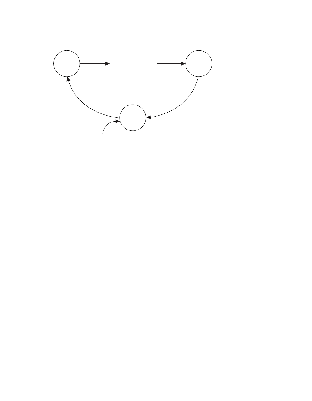
Chapter 3 Timing Diagrams
When REQ Unasserted,
Latch Input Data
Wait
For
REQ
Clear
ACK
Programmable
Delay
Send
ACK
Wait
For
Space
When 6533 Device has
space for data, input data.
When REQ
Asserted
Initial State:
ACK Set
Wait
For
REQ
Figure 3-10. 8255 Emulation Input State Machine
653X User Manual 3-14 ni.com
Page 66
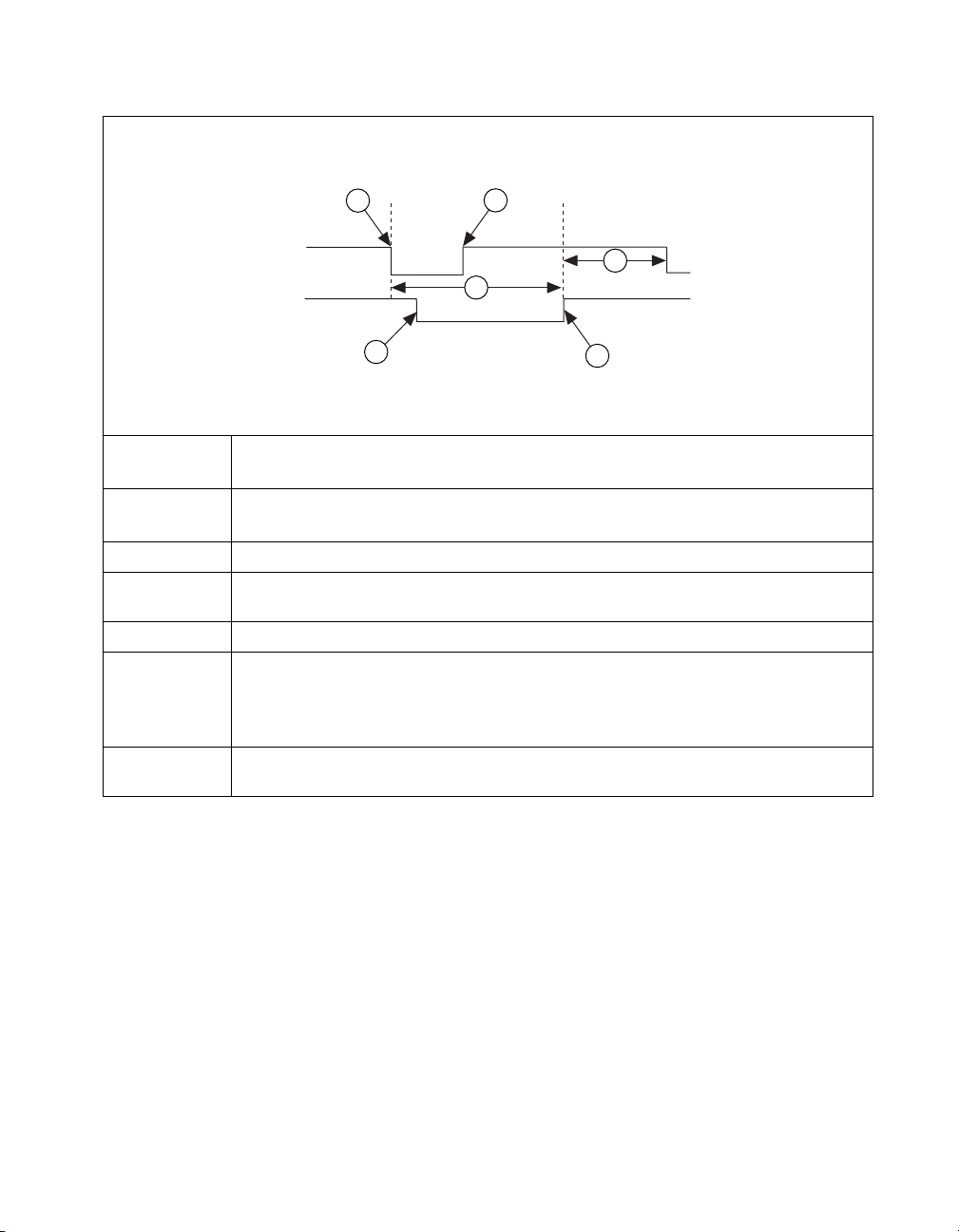
Chapter 3 Timing Diagrams
1
ACK
REQ
2
4
6
3
5
ACK and REQ are shown as active low.
Steps 1-6 are repeated for each transfer.
Reference
Point Action Steps
1 When the 653X device has data to output, it asserts the ACK signal, then waits for
the peripheral device to assert REQ to indicate it is ready to accept data
2
3
The peripheral device asserts a REQ signal to accept the data.
The peripheral device can receive the data on the falling or rising edge of the ACK
signal or any time in between before the next rising edge on REQ.
4
5
The REQ signal edge in step 2 causes the ACK signal to return to deassert.
The rising REQ signal edge enables a new transfer to occur. The peripheral device
should wait until it has received data before deasserting the REQ signal. The
peripheral device can also wait for the ACK signal to deassert before deasserting
the REQ line.
6
The 653X device reasserts the ACK signal when it has data and is ready for
another output. A programmable delay can be inserted here.
Figure 3-11.
© National Instruments Corporation 3-15 653X User Manual
8255 Emulation Output Handshaking Sequence
Page 67

Chapter 3 Timing Diagrams
When REQ
Unasserted
Wait
For
REQ
Clear ACK
Programmable
Delay
Then Send ACK
Initial State: ACK Cleared
Wait
For
Data
When 6533 Device has
data to output, output data.
Output Data,
When REQ
Asserted
Wait
For
REQ
Figure 3-12. 8255 Emulation Output State Machine
653X User Manual 3-16 ni.com
Page 68
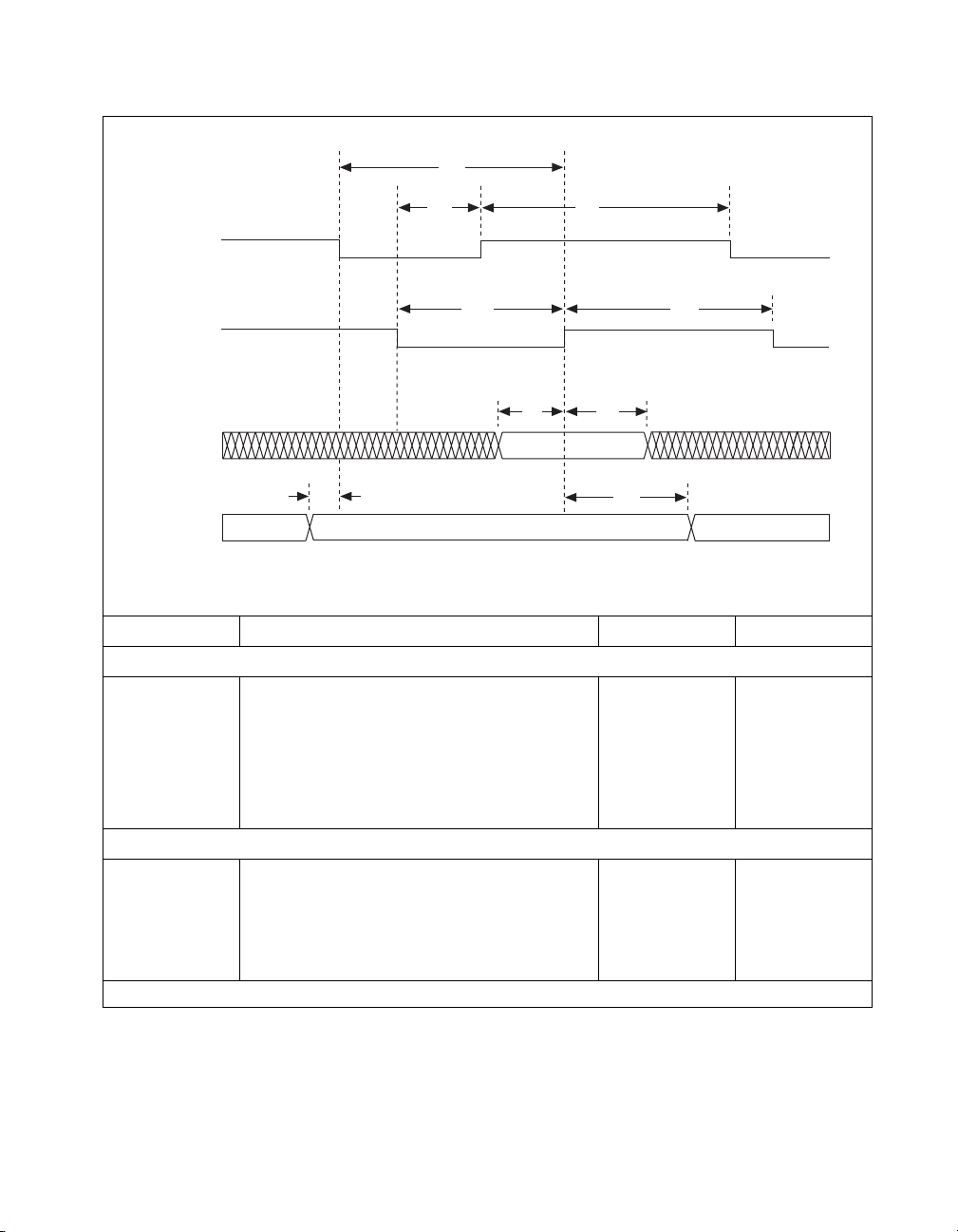
Chapter 3 Timing Diagrams
t
a*r
ACK
REQ
Data In Valid
Data Out Valid
t
doa*
t
r*a
t
r*r
t
aa*
t
rr*
t
dir
t
rdi
t
rdo
ACK and REQ are shown as active low
Parameter Description Minimum Maximum
Input Parameters
t
r*r
t
rr*
t
a*r
t
dir
t
rdi
REQ low duration 75 —
REQ high duration 75 —
ACK falling edge to REQ rising edge 0 —
Input data valid to REQ rising edge 0 —
REQ rising edge to input data invalid 10 —
Output Parameters
t
aa*
t
r*a
t
doa*
t
rdo
All timing values are in nanoseconds.
ACK high duration 100 —
REQ falling edge to ACK rising edge — 150
Output data valid to ACK falling edge 25 —
REQ rising edge to output data invalid 100 —
Figure 3-13.
© National Instruments Corporation 3-17 653X User Manual
8255 Emulation Output Timing Diagram
Page 69

Chapter 3 Timing Diagrams
Using the Level-ACK Protocol
In level-ACK protocol, the 653X device asserts the ACK signal when ready
for a transfer and holds the ACK signal level until an active-going edge
occurs on the REQ line. After the REQ edge occurs, the 653X device
deasserts the ACK signal until the device is ready for another transfer.
1
ACK
REQ
2
Initial State
3
4
ACK and REQ are shown as active high.
Steps 1-4 are repeated for each transfer.
Reference
Point Action Steps
Initial State ACK is deasserted. The 653X device waits for an active REQ to indicate that the
peripheral device is ready. The peripheral device may optionally drive the first
data at this time. The transfer cannot begin until the peripheral asserts REQ; the
peripheral may either pulse REQ, or hold REQ high until the first ACK occurs.
If the peripheral pulses REQ, make sure to start the transfer on the 653X device
before the pulse occurs, to avoid missing the pulse.
1 The 653X device waits until it has space for data, then it asserts ACK.
2 The peripheral device can then strobe data into the 653X device by first
deasserting then asserting the REQ signal. The 653X device waits for an
active-going transition on the REQ line. ACK stays asserted, indicating the
653X device is ready, until the active-going REQ occurs.
3 The active-going REQ signal edge deasserts the ACK signal and causes the
653X device to latch input data.
4 To slow down the data transfer, you can insert a programmable delay before the
ACK signal is asserted.
Figure 3-14.
653X User Manual 3-18 ni.com
Level ACK Input Handshaking Sequence
Page 70

Initial State: ACK Cleared
When REQ
Wait
Asserted
For
REQ
Clear ACK
When REQ
Unasserted
Programmable
Delay
Wait
For
REQ
Chapter 3 Timing Diagrams
Wait
For
Space
When 6533 Device has space
for data, input data.*
Programmable
Delay
Send
ACK
* With REQ-edge latching enabled, the data input
is from the last active-going REQ edge.
Figure 3-15.
Level ACK Input State Machine
© National Instruments Corporation 3-19 653X User Manual
Page 71

Chapter 3 Timing Diagrams
ACK
REQ
t
aa*
t
ra*
t
ar
t
r*r
t
rr*
Input Data Valid
(REQ-edge
latching)
Input Data Valid
(REQ-edge
latching disabled)
t
dir(1)
t
dir(2)
t
rdi
t
adi
ACK and REQ are shown as active high
Parameter Description Minimum Maximum
Input Parameters
t
t
t
t
dir(1)
rr*
r*r
ar
REQ pulse width 75 —
REQ inactive duration 75 —
ACK to next REQ 0 —
Input data setup to REQ active
0 —
(with REQ-edge latching)
t
rdi
Input data hold from REQ active
10 —
(with REQ-edge latching)
t
dir(2)
Input data setup to REQ
0 —
(with REQ-edge latching disabled)
t
adi
Input data hold from ACK
0 —
(with REQ-edge latching disabled)
Output Parameters
t
aa*
t
ra*
All timing values are in nanoseconds.
ACK pulse width 225 —
REQ to ACK inactive 100 200
Figure 3-16. Level ACK Input Timing Diagram
653X User Manual 3-20 ni.com
Page 72

Chapter 3 Timing Diagrams
Note
With REQ edge latching enabled (default), the REQ edge determines when data
will be latched. Input data valid has to be held before the active going REQ edge a
minimum of t
ns. With REQ edge disabled, input data valid has to be held t
rdi
after the
adi
next active going ACK signal edge is asserted.
Initial State
ACK
REQ
1
2
3
4
ACK and REQ are shown as active high.
Steps 1-4 are repeated for each transfer.
Reference
Point Action Steps
Initial State ACK is deasserted.
1 When the 653X device has data to output, it drives the data onto the data lines,
and then asserts ACK. ACK stays asserted, indicating the 653X device is ready,
until the active-going REQ edge occurs.
2 The peripheral device responds with an active-going REQ signal edge. ACK
stays asserted, indicating the 653X device is ready, until the active-going REQ
occurs. Since the REQ is already asserted, the 653X device will wait until it
deasserts and reasserts to deassert the ACK signal and request additional data.
3 The asserted REQ signal deasserts the ACK signal.
4 To slow down the data transfer, you can insert a programmable delay before the
ACK signal is asserted.
Figure 3-17.
© National Instruments Corporation 3-21 653X User Manual
Level ACK Output Handshaking Sequence
Page 73

Chapter 3 Timing Diagrams
When REQ
Wait
Asserted
For
REQ
Clear ACK
When REQ
Unasserted
Programmable
Delay
Wait
For
REQ
Initial State: ACK Cleared
Wait
For
Data
When 6533 Device has data
to output, output data.*
Programmable
Delay
Send
ACK
* With REQ-edge latching enabled, the data output is
delayed until the next inactive-going REQ edge.
Figure 3-18. Level ACK Output State Machine
653X User Manual 3-22 ni.com
Page 74

ACK
REQ
Chapter 3 Timing Diagrams
t
aa*
t
ar
t
r*r
t
rr*
Output Data Valid
(REQ-edge
latching)
Output Data Valid
(REQ-edge
latching disabled)
t
ra*
t
doa
t
rdo
ACK and REQ are shown as active high
t
r*do
Parameter Description Minimum Maximum
Input Parameters
t
rr*
t
r*r
t
ar
REQ pulse width 75 —
REQ inactive duration 75 —
ACK to next REQ 0 —
Output Parameters
t
t
aa*
t
r*do
ra*
ACK pulse width 225 —
REQ to ACK inactive 100 200
REQ inactive to new output data
050
(with REQ-edge latching)
t
rdo
REQ to new output data
0—
(with REQ-edge latching disabled)
t
doa
Output data valid to ACK
25
1
—
(with REQ-edge latching disabled)
1
(min.) = 25 + programmable delay
t
doa
Figure 3-19.
Note
With REQ edge latching disabled (default), output data valid will hold t
Level ACK Output Timing Diagram
rdo
ns after
the REQ edge is asserted. With REQ edge latching enabled, that data will be held for at
most t
© National Instruments Corporation 3-23 653X User Manual
ns after the REQ edge deasserts.
rdo
Page 75

Chapter 3 Timing Diagrams
Using Protocols Based on Signal Edges
The 653X device can communicate via pulses on the ACK and REQ lines.
The three edge protocols are:
• Trailing-edge protocol—The trailing edge of the ACK or REQ pulse
indicates that the 653X device or peripheral device is ready for a
transfer.
• Leading-edge protocol—The rising edge of the ACK or REQ pulse
indicates that the 653X device or peripheral device is ready for a
transfer
• Long-pulse protocol—This is a variant of the leading-edge protocol,
with the additional option of using a data-settling delay. If your
application requires a large minimum pulse width, you would want to
use this protocol. In this case, the programmable delay is used to
increase the ACK pulse width instead of delaying the ACK pulse.
You can also use long-pulse protocol to handshake with an actual 8255 or
82C55 PPI. You must set the ACK and REQ signals to active low and select
a minimum pulse width of 500 ns for your 8255 or 82C55.
653X User Manual 3-24 ni.com
Page 76

Using the Trailing-Edge Protocol
Chapter 3 Timing Diagrams
ACK
REQ
Initial State
1
Data Latched
2
ACK and REQ are shown as active high.
Steps 1-2 are repeated for each transfer.
3
Reference
Point Action Steps
Initial State ACK is deasserted. The 653X device waits for the peripheral device to pulse
REQ to indicate it has data.
1 The 653X device sends an ACK pulse of programmable width when ready to
receive data.
2 After receiving the trailing edge of the ACK pulse, the peripheral device can
strobe data into the 653X device and pulse the REQ.
3 The 653X device sends another ACK pulse when ready for another input.
Wait
For
REQ
When REQ
Unasserted
When REQ
Asserted
Initial State: ACK Cleared
Figure 3-20.
Programmable
Delay
Wait
For
REQ
Trailing Edge Input Handshaking Sequence
Wait
For
Space
Send
ACK
Programmable
Delay
Clear
ACK
* With REQ-edge latching enabled, the data input
is from the last inactive-going REQ edge.
When 6533 Device
has space for data,
input data.*
Figure 3-21.
© National Instruments Corporation 3-25 653X User Manual
Trailing Edge Input State Machine
Page 77
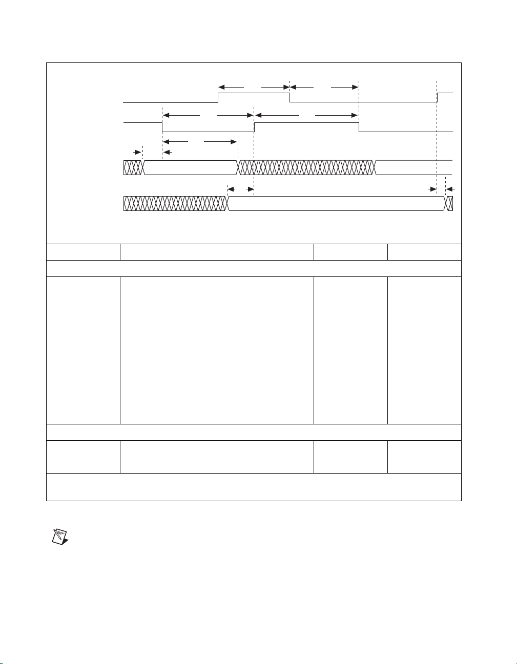
Chapter 3 Timing Diagrams
ACK
REQ
Input Data Valid
(REQ-edge
latching)
Input Data Valid
(REQ-edge
latching disabled)
t
aa*
t
r*r
t
t
dir*
r*di
t
dir
t
a*r*
t
rr*
t
adi
ACK and REQ are shown as active high
Parameter Description Minimum Maximum
Input Parameters
t
rr*
t
r*r
t
dir*
REQ pulse width 75 —
REQ inactive duration 75 —
Input data setup to REQ inactive
0 —
(with REQ-edge latching)
t
r*di
Input data hold from REQ inactive
10 —
(with REQ-edge latching)
t
dir
Input data setup to REQ
0 —
(with REQ-edge latching disabled)
t
adi
Input data hold from ACK
0 —
(with REQ-edge latching disabled)
Output Parameters
t
aa*
t
a*r*
1
t
(min.) = 225 + programmable delay
aa*
2
t
(max) = 275 + programmable delay
aa*
ACK pulse width 225
ACK inactive to next REQ inactive 0 —
1
275
2
Figure 3-22. Trailing Edge Input Timing Diagram
Note
When REQ-edge latching is enabled (default), the REQ edge determines when data
will be latched. Input data valid needs to be held t
When REQ-edge latching is disabled, input data valid needs to be held t
after the trailing edge of REQ occurs.
r*di
after the active
adi
going edge of the ACK signal occurs.
653X User Manual 3-26 ni.com
Page 78

Initial State
Chapter 3 Timing Diagrams
ACK
REQ
1
2
ACK and REQ are shown as active high.
Steps 1-2 are repeated for each transfer.
Reference
Point Action Steps
Initial State ACK is deasserted.
1 The 653X device sends an ACK pulse of programmable width. This indicates
new, valid output data.
2 The peripheral device responds with a REQ pulse. The trailing edge of the REQ
pulse deasserts the ACK signal and requests additional data.
Trailing Edge Output Handshaking Sequence
Initial State: ACK Cleared
Wait
For
Data
Send
ACK
When 6533 Device has
data to output, output data.*
Wait
For
REQ
When REQ
Unasserted
Figure 3-23.
Programmable
Delay
Programmable
Delay
Clear
When REQ
Asserted
© National Instruments Corporation 3-27 653X User Manual
Wait
For
REQ
ACK
* With REQ-edge latching enabled, the data output is
delayed until the next inactive-going REQ edge.
Figure 3-24.
Trailing Edge Output State Machine
Page 79

Chapter 3 Timing Diagrams
ACK
REQ
Output Data Valid
(REQ-edge
latching)
Output Data Valid
(REQ-edge
latching disabled)
t
aa*
t
r*r
t
doa
t
a*r*
t
rr*
t
r*do(1)
t
r*do(2)
ACK and REQ are shown as active high
Parameter Description Minimum Maximum
Input Parameters
t
t
t
rr*
r*r
a*r*
REQ pulse width 75 —
REQ inactive duration 75 —
ACK inactive to next REQ inactive 0 —
Output Parameters
t
t
r*do(1)
aa*
ACK pulse width 225
REQ inactive to new output data
050
1
275
2
(with REQ-edge latching)
t
r*do(2)
REQ inactive to new output data
0 —
(with REQ-edge latching disabled)
t
doa
Output data valid to ACK
25 —
(with REQ-edge latching disabled)
1
t
2
t
aa*
aa*
= 225 + programmable delay
(min)
(max) = 275 + programmable delay
Figure 3-25. Trailing Edge Output Timing Diagram
Note
When REQ-edge latching is disabled (default), output data valid will be held
t
ns after the trailing edge of REQ occurs. With REQ-edge latching enabled, output
r*do(1)
data will be held at most t
653X User Manual 3-28 ni.com
ns after the trailing edge of REQ occurs.
r*do(1)
Page 80

Using the Leading-Edge Protocol
Chapter 3 Timing Diagrams
ACK
REQ
1
Initial State
3
2
ACK and REQ are shown as active high.
Steps 1-3 are repeated for each transfer.
4
Reference
Point Action Steps
Initial State ACK is deasserted. The 653X device waits for an active REQ to indicate that the
peripheral device is ready. The peripheral device may optionally drive the first
data at this time. The transfer cannot begin until the peripheral asserts REQ: the
peripheral may either pulse REQ, or hold REQ high until the first ACK occurs.
If the peripheral pulses REQ, make sure to start the transfer on the 653X device
before the pulse occurs, to avoid missing the pulse.
1 The 653X device sends an ACK pulse when it is ready to receive data. The ACK
pulse width is fixed, assuming the peripheral device has deasserted the REQ
signal. Otherwise the ACK signal remains asserted until the REQ signal
deasserts.
2 After receiving at least the leading edge of the ACK pulse, the peripheral device
can strobe data into the 653X device by asserting REQ.
3 To slow down the data transfer, you can insert a programmable delay before the
ACK signal is asserted.
4 The 653X device sends another ACK when it is ready for another input.
Figure 3-26.
© National Instruments Corporation 3-29 653X User Manual
Leading Edge Input Handshaking Sequence
Page 81

Chapter 3 Timing Diagrams
Initial State: ACK Cleared
When REQ
Wait
For
REQ
Asserted
When REQ
Unasserted
Clear
ACK
Pulse
Programmable
Delay
Wait
For
REQ
Figure 3-27. Leading Edge Input State Machine
Wait
For
Space
When 6533 Device has space
for data, input data.*
Programmable
Send
ACK
Pulse
* With REQ-edge latching enabled, the data input
Delay
is from the last active-going REQ edge.
653X User Manual 3-30 ni.com
Page 82

ACK
REQ
Chapter 3 Timing Diagrams
t
aa*
t
r*a*
t
ar
t
r*r
t
rr*
Input Data Valid
(REQ-edge
latching)
Input Data Valid
(REQ-edge
latching disabled)
t
dir(1)
t
dir(2)
t
rdi
t
adi
ACK and REQ are shown as active high
Parameter Description Minimum Maximum
Input Parameters
t
t
t
t
dir(1)
rr*
r*r
ar
REQ pulse width 75 —
REQ inactive duration 75 —
ACK to next REQ 0 —
Input data setup to REQ active
0 —
(with REQ-edge latching)
t
rdi
Input data hold from REQ active
10 —
(with REQ-edge latching)
t
dir(2)
Input data setup to REQ
0 —
(with REQ-edge latching disabled)
t
adi
Input data hold from ACK
0 —
(with REQ-edge latching disabled)
Output Parameters
t
aa*
t
r*a*
All timing values are in nanoseconds.
ACK pulse width 125 —
REQ inactive to ACK inactive 150 —
Figure 3-28.
© National Instruments Corporation 3-31 653X User Manual
Leading Edge Input Timing Diagram
Page 83

Chapter 3 Timing Diagrams
Note
With REQ edge latching enabled (default), the REQ edge determines when data will
be latched. Input data valid has to be held before an active going REQ edge a minimum of
t
ns. With REQ edge disabled, it has to be held t
rdi
edge occurs.
after the next active-going ACK signal
adi
Initial State
ACK
REQ
1
3
2
ACK and REQ are shown as active high.
Steps 1-3 are repeated for each transfer.
Reference
Point Action Steps
Initial State ACK is deasserted.
1 The 653X device sends the ACK pulse after driving output data to indicate that it
has new, valid output data. The ACK pulse width is fixed, assuming the peripheral
device has deasserted the REQ signal. Otherwise, the ACK signal remains
asserted until the peripheral device deasserts the REQ signal.
2
Once the data is latched, the peripheral device must respond with an active-going
REQ signal edge to request additional data.
3
To slow down the data transfer, you can insert a programmable delay before the
ACK signal is asserted.
Figure 3-29. Leading Edge Output Handshaking Sequence
653X User Manual 3-32 ni.com
Page 84

Wait
For
REQ
When REQ
Asserted
Clear
ACK
Pulse
When REQ
Unasserted
Programmable
Delay
Wait
For
REQ
Chapter 3 Timing Diagrams
Initial State: ACK Cleared
Wait
For
Data
When 653
data to output, output data.*
Programmable
Send
ACK
Pulse
* With REQ-edge latching enabled, the data output is
delayed until the next inactive-going REQ edge.
Delay
X
Device has
Figure 3-30.
Leading Edge Output State Machine
© National Instruments Corporation 3-33 653X User Manual
Page 85

Chapter 3 Timing Diagrams
t
aa*
ACK
t
r*a*
REQ
Output Data Valid
(REQ-edge
latching disabled)
t
Output Data Valid
(REQ-edge
latching)
t
doa
t
ar
r*r
t
rr*
t
rdo
t
r*do
ACK and REQ are shown as active high
Parameter Description Minimum Maximum
Input Parameters
t
rr*
t
r*r
t
ar
REQ pulse width 75 —
REQ inactive duration 75 —
ACK to next REQ 0 —
Output Parameters
t
t
t
aa*
r*a*
r*do
ACK pulse width 125 —
REQ inactive to ACK inactive 150 —
REQ inactive to new output data
050
(with REQ-edge latching)
t
rdo
REQ to new output data
0—
(with REQ-edge latching disabled)
t
doa
Output data valid to ACK
25
1
(with REQ-edge latching disabled)
1
(min.) = 25 + programmable delay
t
doa
—
Figure 3-31. Leading Edge Output Timing Diagram
Note
With REQ edge latching disabled (default), output data valid will hold t
rdo
ns after
the REQ edge occurs. With REQ edge latching enabled, that data will be held for at most
t
ns after the REQ edge deasserts.
rdo
653X User Manual 3-34 ni.com
Page 86

Using the Long-Pulse Protocol
1
Chapter 3 Timing Diagrams
ACK
REQ
Initial State
2
3
ACK and REQ are shown as active high.
Steps 1-4 are repeated for each transfer.
4
Reference
Point Action Steps
Initial State ACK is deasserted. The 653X device waits for an active REQ to indicate that the
peripheral device is ready. The peripheral device may optionally drive the first
data at this time. The transfer cannot begin until the peripheral asserts REQ: the
peripheral may either pulse REQ, or hold REQ high until the first ACK occurs.
If the peripheral pulses REQ, make sure to start the transfer on the 653X device
before the pulse occurs, to avoid missing the pulse.
1 The 653X device asserts an ACK signal when it is ready to receive data,
assuming the peripheral device has deasserted the REQ signal. Otherwise,
the ACK signal remains asserted until the REQ signal deasserts.
2 To slow down the data transfer, you can insert a programmable delay before
deasserting the ACK signal. Unlike in the leading-edge protocol, the pulse width
is programmable.
3 After receiving the leading edge of the ACK pulse, the peripheral device can
strobe data into the 653X device by asserting REQ.
4 The same programmable delay that controls the minimum ACK pulse width
further slows down the transfer by delaying next occurrence of the next ACK
pulse.
Figure 3-32.
© National Instruments Corporation 3-35 653X User Manual
Long Pulse Input Handshaking Sequence
Page 87

Chapter 3 Timing Diagrams
Initial State: ACK Cleared
When REQ
Wait
For
REQ
Asserted
Clear
ACK
Pulse
Programmable
Delay
Wait
Space
Send
ACK Pulse
Programmable
Delay
For
When 6533 Device has
space for data, input data.*
When REQ
Unasserted
Wait
For
REQ
* With REQ-edge latching enabled, the data input
is from the last active-going REQ edge.
Figure 3-33. Long Pulse Input State Machine
653X User Manual 3-36 ni.com
Page 88

ACK
REQ
Chapter 3 Timing Diagrams
t
aa*
t
r*a*
t
ar
t
r*r
t
rr*
Input Data Valid
(REQ-edge
latching)
Input Data Valid
(REQ-edge
latching disabled)
t
dir(1)
t
dir(2)
t
rdi
t
adi
ACK and REQ are shown as active high
Parameter Description Minimum Maximum
Input Parameters
t
t
t
t
dir(1)
rr*
r*r
ar
REQ pulse width 75 —
REQ inactive duration 75 —
ACK to next REQ 0 —
Input data setup to REQ active
0 —
(with REQ-edge latching)
t
rdi
Input data hold from REQ active
10 —
(with REQ-edge latching)
t
dir(2)
Input data setup to REQ
0 —
(with REQ-edge latching disabled)
t
adi
Input data hold from ACK
0 —
(with REQ-edge latching disabled)
Output Parameters
t
aa*
t
r*a*
1
t
(min.) = 125 + programmable delay
aa*
ACK pulse width 125
REQ inactive to ACK inactive 150 —
1
—
Figure 3-34.
© National Instruments Corporation 3-37 653X User Manual
Long Pulse Input Timing Diagram
Page 89

Chapter 3 Timing Diagrams
Note
With REQ edge latching enabled (default) REQ edge determines when data will be
latched. Input data valid has to be held before active going REQ edge a minimum of t
With REQ edge disabled, it has to be held t
occurs.
after the next active going ACK signal edge
adi
rdi
ns.
Initial State
ACK
REQ
1
2
*
3
ACK and REQ are shown as active high.
Steps 1-3 are repeated for each transfer.
= programmable pulse width
*
Reference
Point Action Steps
Initial State ACK is deasserted.
1 The 653X device sends an ACK pulse with programmable width to indicate that
it has data to output. Assuming the peripheral device has deasserted the REQ
signal. Otherwise, the ACK signal remains asserted until the peripheral device
deasserts the REQ signal.
2 The peripheral device can latch the data on the rising or falling edge of the ACK
pulse, or anytime before asserting the REQ signal.
3 Once the data is latched, the peripheral device must respond with an active-going
REQ signal edge.
Figure 3-35. Long Pulse Output Handshaking Sequence
653X User Manual 3-38 ni.com
Page 90

Wait
For
REQ
When REQ
Asserted
Clear
ACK
Pulse
Programmable
Delay
Initial State: ACK Cleared
Wait
For
Data
Send
ACK Pulse
Programmable
Delay
When 6533 Device has
data to output, output data.*
Chapter 3 Timing Diagrams
When REQ
Unasserted
Wait
For
REQ
* With REQ-edge latching enabled, the data output is
delayed until the next inactive-going REQ edge.
Figure 3-36.
Long Pulse Output State Machine
© National Instruments Corporation 3-39 653X User Manual
Page 91

Chapter 3 Timing Diagrams
t
aa*
ACK
t
ar
REQ
Output Data Valid
(REQ-edge
latching disabled)
Output Data Valid
(REQ-edge
latching)
t
r*r
t
doa
t
rr*
t
rdo
t
r*do
ACK and REQ are shown as active high
Parameter Description Minimum Maximum
Input Parameters
t
rr*
t
r*r
t
ar
REQ pulse width
REQ inactive duration
ACK to next REQ
75 —
75 —
0 —
Output Parameters
t
t
aa*
r*do
ACK pulse width
REQ inactive to new output data
1
125
050
(with REQ-edge latching)
t
rdo
REQ to new output data
0 —
(with REQ-edge latching disabled)
t
doa
Output data valid to ACK
25 —
(with REQ-edge latching disabled)
1
t
(min.) = 125 + programmable delay
aa*
—
Figure 3-37. Long Pulse Output Timing Diagram
Note
With REQ edge latching disabled (default), output data valid will hold t
the REQ edge with REQ edge latching enabled, that data will be held for at most t
ns after
rdo
rdo
ns
after the REQ edge deasserts.
653X User Manual 3-40 ni.com
Page 92

Specifications
This appendix lists features and specifications for your 653X devices and
the PCI/PXI-7030/6533 device. Specifications are typical at 25 °C unless
otherwise noted.
Digital I/O
Number of channels ............................... 32 input/output;
Compatibility ......................................... TTL/CMOS (standard or
Hysteresis ............................................... 500 mV
Digital logic levels
Input low voltage 0V 0.8 V
A
4 dedicated output and control;
4 dedicated input and status
wired-OR)
Level Min Max
Input high voltage 2V 5V
Input low current for data lines
(V
= 0.4 V)
in
DPULL high
DPULL low
Input high current for data lines
(V
= 2.4 V)
in
DPULL high
DPULL low
Input low current for control lines
(V
= 0.4 V)
in
CPULL high
CPULL low
© National Instruments Corporation A-1 653X User Manual
—
—
—
—
—
—
–70 µA
–10 µA
10 µA
40 µA
–2.5 mA
–200 µA
Page 93
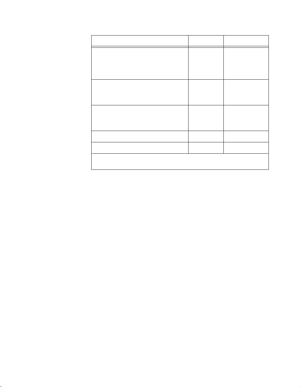
Appendix A Specifications
Level (Continued) Min Max
Input high current for control lines
(V
= 2.4 V)
in
CPULL high
CPULL low
—
—
200 µA
1.4 mA
Input low current for CPULL/DPULL
(V
= 0.4 V)
in
— 4 µA
Input high current for
CPULL/DPULL
(V
= 2.4 V) — 140 µA
in
Output low voltage (IOL = 24 mA) — 0.4 V
Output high voltage* (IOH = 24 mA) 2.4 V —
* When configured as standard outputs. Drivers configured as wired-OR outputs are in the
high-impedance state when logically high.
Absolute max input voltage range ..........–0.3 to 5 V
Memory
Power-on state for outputs ......................High-impedance, pulled up or
down (selectable)
Data transfers
(all devices except DAQCard)................Interrupt, DMA
AT-DIO-32HS ........................................16 S
DAQCard-6533 for PCMCIA ................16 S
PCI/PXI-6534 .........................................64 MB, two 32 MB modules
on each 6534 device
PCI/PXI-7030/6533 ................................16 S
PCI-DIO-32HS .......................................16 S
PXI-6533 ................................................16 S
653X User Manual A-2 ni.com
Page 94

Pattern I/O
Appendix A Specifications
Direction................................................. Input or output
Change Detection
Triggers
Maximum sample rate (internally
timed, for small transfers
Minimum sample rate
(internal clock rate) ................................ 1 S/10 min.
Change-detection resolution ..................150 ns
1
)..................... 20 MHz
Start and Stop Triggers
Compatibility ......................................... TTL/CMOS
Trigger types .......................................... Rising or falling edge,
or digital pattern
Pulse width for edge triggers (min.)....... 10 ns
Pattern trigger detection
capabilities ............................................. Detect pattern match or mismatch
on user-selected data lines
Pattern trigger resolution........................ 60 ns or one REQ period,
depending on pattern I/O mode
RTSI Triggers (PCI, PXI, AT)
Trigger lines ........................................... 7
Bus Interfaces
PCI-DIO-32HS/PXI-6533/
PCI-6534/PXI-6534/
AT-DIO-32HS type................................ AT slave with dual DMA
DAQCard-6533 for PCMCIA type ........ PCMCIA slave
1
Small transfer size is the size of the FIFO.
© National Instruments Corporation A-3 653X User Manual
Page 95

Appendix A Specifications
Power Requirement
+5 VDC (±5%)
(with light output load) ...........................500 mA
Power Available at I/O Connector
PCI-DIO-32HS, PXI-6533,
AT-DIO-32HS,
PCI-6534, and PXI-6534 ........................+4.65 to +5.25 VDC at 1 A
DAQCard-6533 for PCMCIA ................+4.65 to +5.25 VDC at 250 mA
Physical
Dimensions, not including connectors
DAQCard-6533 for PCMCIA .........3.4 by 2.1 in.
AT-DIO-32HS/PCI-653X................6.9 by 4.2 in.
PXI-653X.........................................6.4 by 3.9 in.
I/O connector
PCI-DIO-32HS, PXI-6533,
AT-DIO-32HS,
PCI-6534, and PXI-6534 .................68-pin male SCSI-II type
DAQCard-6533 for PCMCIA .........68-pin female PCMCIA
connector
Environment
Operating temperature ............................0 to 55 °C
Storage temperature ................................–20 to 70 °C
Relative humidity ...................................5 to 90% noncondensing
Functional shock.....................................MIL-T-28800 E Class 3
(per Section 4.5.5.4.1)
Half-sine shock pulse, 11 ms
duration, 30 g peak, 30 shocks
per face
Operational random vibration
(PXI only) ...............................................5 to 500 Hz, 0.31 g
653X User Manual A-4 ni.com
, 3 axes
rms
Page 96

Appendix A Specifications
Nonoperational random vibration
(PXI only) .............................................. 5 to 500 Hz, 2.5 g
Note
Random vibration profiles were developed in accordance with MIL-T-28800E and
, 3 axes
rms
MIL-STD-810E Method 514. Test levels exceed those recommended in MIL-STD-810E
for Category 1 (Basic Transportation, Figures 514.4-1 through 514.4-3).
© National Instruments Corporation A-5 653X User Manual
Page 97

Using PXI with CompactPCI
You can use your PXI-653X device as a plug-in device in a standard
CompactPCI chassis, but you will not be able to access PXI-specific
functions, such as RTSI bus features detailed in the PXI Specification,
rev. 1.0.
The CompactPCI specification permits vendors to develop sub-buses that
coexist with the basic PCI interface on the CompactPCI bus. Compatible
operation is not guaranteed between CompactPCI devices with different
sub-buses nor between CompactPCI devices with sub-buses and PXI.
The standard implementation for CompactPCI does not include these
sub-buses. Your PXI-653X device will work in any standard CompactPCI
chassis adhering to the PICMG CompactPCI 2.0 R2.1 document.
PXI-specific features are implemented on the J2 connector of the
CompactPCI bus. The following table lists the J2 pins used by your
PXI-653X device. Your PXI device is compatible with any CompactPCI
chassis with a sub-bus that does not drive these lines. Even if the sub-bus is
capable of driving these lines, the PXI device is still compatible as long as
those pins on the sub-bus are disabled by default and not ever enabled.
B
Table B-1.
PXI-653X
Signal
RTSI Trigger
(0..6)
Reserved PXI Star D17
RTSI Clock PXI Trigger (7) E16
Reserved LBR (7, 8, 10, 11, 12) A3, C3, E3, A2, B2
© National Instruments Corporation B-1 653X User Manual
J2 Pins Used by Your PXI-653X Device
PXI Pin Name PXI J2 Pin Number
PXI Trigger (0..6) B16, A16, A17, A18, B18,
C18, E18
Page 98

Connecting Signals with
Accessories
This appendix describes how to connect signals to your 653X device. Use
the first part of the appendix to acquaint yourself with the device control
signals. Then go to appropriate pinout diagrams (68 or 50-pin), which
display the layout of pin locations.
Control Signals
Use the four control signals to regulate/control the timing of your data
transfer when using the handshaking and pattern I/O modes. The direction
and function of each signal varies, depending on the mode of operation,
as shown in Table C-1.
C
Table C-1.
Signal Name
REQ<1..2> Input Request—Indicates
ACK<1..2>
or
STARTTRIG<1..2>
STOPTRIG<1..2> N/A N/A Input Stop trigger
PCLK<1..2> Input or
© National Instruments Corporation C-1 653X User Manual
Direction Function Direction Function
Control Signals for Handshaking I/O and Pattern I/O
Handshaking I/O Pattern I/O
Input or
that the peripheral
device is ready
Output Acknowledge—
Indicates the 653X
device is ready
Peripheral clock N/A N/A
Output
Output
Input Start trigger
Request—
Clocks the data transfer
Page 99

Appendix C Connecting Signals with Accessories
Making 68-Pin Signal Connections
Caution
Do not make connections that exceed any of the maximum input or output ratings
on the 653X, listed in Appendix A, Specifications. This includes connecting any power
signals to ground and vice versa. Doing so may damage your device and your computer.
National Instruments is not liable for any damages resulting from these types of
signal connections.
34 68
DIOD7
GND
DIOD4
DIOD3
GND
DIOD0
DIOC7
GND
DIOC4
DIOC3
GND
DIOC0
DIOB7
DIOB6
GND
RGND
GND
DIOB1
DIOB0
DIOA7
GND
DIOA4
DIOA3
GND
DIOA0
REQ2*
ACK2 (STARTTRIG2)*
STOPTRIG2
PCLK2
PCLK1
STOPTRIG1
ACK1 (STARTTRIG1)*
REQ1*
+5 V
33 67
32 66
31 65
30 64
29 63
28 62
27 61
26 60
25 59
24 58
23 57
22 56
21 55
20 54
19 53
18 52
17 51
16 50
15 49
14 48
13 47
12 46
11 45
10 44
943
842
741
640
539
438
337
236
135
GND
DIOD6
DIOD5
GND
DIOD2
DIOD1
GND
DIOC6
DIOC5
GND
DIOC2
DIOC1
RGND
GND
DIOB5
DIOB4
DIOB3
DIOB2
GND
GND
DIOA6
DIOA5
GND
DIOA2
DIOA1
RGND
GND
GND
CPULL
GND
DPULL
GND
GND
RGND
Figure C-1.
653X I/O Connector 68-Pin Assignments
653X User Manual C-2 ni.com
Page 100

Appendix C Connecting Signals with Accessories
Note
In Figure C-1, the * indicates that you can reverse the pin assignments of the ACK1
(STARTTIG1) and REQ1 pins, or the ACK2 (STARTTIG2) and REQ2 pins. To do this, set
the
ACK-REQ Exchange
set_DAQ_Device_Info
attribute to ON in the DIO Parameter VI in LabVIEW or in
in NI-DAQ. This allows you to perform handshaking I/O
between two 653X devices using an SH-68-68-D1 cable.
Use Table C-2 to find the accessories designed for connecting signals to
your 653X device.
Device Shielded Cable Ribbon Cable Cable Adapter
PCI/PXI/AT/
Compact PCI
SHC68-68-D1—female 68-pin
SCXI connectors on both ends
of the cable
DAQCard-6533
for PCMCIA
PSHR68-68-D1 and
PSHR68-68M
Signal Descriptions
Use Table C-3 to find the function for each signal, which is based on the
mode and protocol you are using. All the signals on the 653X device are
referenced to the GND lines.
Table C-2.
68-Pin Accessories
N/A N/A
PR68-68F N/A
© National Instruments Corporation C-3 653X User Manual
 Loading...