

Page 1

DAQ
6023E/6024E/6025E User Manual
Multifunction I/O Devices for PCI, PXI ,
CompactPCI, and PCMCIA Bus Computers
6023E/6024E/6025E User Manual
December 2000 Edition
Part Number 322072C-01
Page 2

Support
Worldwide Technical Support and Product Information
ni.com
National Instruments Corporate Headquarters
11500 North Mopac Expressway Austin, Texas 78759-3504 USA Tel: 512 794 0100
Worldwide Offices
Australia 03 9879 5166, Austria 0662 45 79 90 0, Belgium 02 757 00 20, Brazil 011 284 5011,
Canada (Calgary) 403 274 9391, Canada (Ottawa) 613 233 5949, Canada (Québec) 514 694 8521,
China (Shanghai) 021 6555 7838, China (ShenZhen) 0755 3904939, Denmark 45 76 26 00,
Finland 09 725 725 11, France 01 48 14 24 24, Germany 089 741 31 30, Greece 30 1 42 96 427,
Hong Kong 2645 3186, India 91805275406, Israel 03 6120092, Italy 02 413091, Japan 03 5472 2970,
Korea 02 596 7456, Mexico 5 280 7625, Netherlands 0348 433466, New Zealand 09 914 0488,
Norway 32 27 73 00, Poland 0 22 528 94 06, Portugal 351 1 726 9011, Singapore 2265886, Spain 91 640 0085,
Sweden 08 587 895 00, Switzerland 056 200 51 51, Taiwan 02 2528 7227, United Kingdom 01635 523545
For further support information, see the Technical Support Resources appendix. To comment on the
documentation, send e-mail to techpubs@ni.com
© Copyright 1998, 2000 National Instruments Corporation. All rights reserved.
Page 3

Important Information
Warranty
The DAQCard-6024E, PCI-6023E, PCI-6024E, PCI-6025E, and PXI-6025E devices are warranted against defectsin materials and
workmanship for a period of one year from the date of shipment, as evidenced by receipts or other documentation. National
Instruments will, at its option, repair or replace equipment that proves to be defective during the warranty period. This warranty
includes parts and labor.
The media on which you receive National Instruments software are warranted not to fail to execute programming instructions,
due to defects in materials and workmanship, for a period of 90 days from date of shipment, as evidenced by receipts or other
documentation. National Instruments will, at its option, repair or replace software media that do not execute programming
instructions if National Instruments receives notice of such defects during the warranty period. National Instruments does not
warrant that the operation of the software shall be uninterrupted or error free.
A Return Material Authorization (RMA) number must be obtained from the factory and clearly marked on the outside of
the package before any equipment will be accepted for warranty work. National Instruments will pay the shipping costs of
returning to the owner parts which are covered by warranty.
National Instruments believes that the information in this document is accurate. The document has been carefully reviewed
for technical accuracy. In the event that technical or typographical errors exist, National Instruments reserves the right to
make changes to subsequent editions of this document without prior notice to holders of this edition. The reader should consult
National Instruments if errors are suspected. In no event shall National Instruments be liable for any damages arising out of
or related to this document or the information contained in it.
E
XCEPT AS SPECIFIED HEREIN,NATIONAL INSTRUMENTS MAKES NO WARRANTIES, EXPRESS OR IMPLIED, AND SPECIFICALLY DISCLAIMS ANY
Copyright
WARRANTY OF MERCHANTABILITY OR FITNESS FOR A PARTICULAR PURPOSE
NEGLIGENCE ON THE PART OF
INSTRUMENTS WILL NOT BE LIABLE FOR DAMAGES RESULTING F ROM LOSS OF DATA, PROFITS, USE OF PRODUCTS, OR INCIDENTAL OR
CONSEQUENTIAL DAMAGES
apply regardless of the form of action, whether in contract or tort, including negligence. Any action against National Instruments
must be brought within one year after the cause of action accrues. National Instruments shall not be liable for any delay in
performance due to causes beyond its reasonable control. The warranty provided herein does not cover damages, defects,
malfunctions, or service failures caused by owner’s failure to follow the National Instruments installation, operation, or
maintenance instructions; owner’s modification of the product; owner’s abuse, misuse, or negligent acts; and power failure or
surges, fire, flood, accident, actions of third parties, or other events outside reasonable control.
Under the copyright laws, this publication may not be reproduced or transmitted in any form, electronic or mechanical, including
photocopying, recording, storing in an information retrieval system, or translating, in whole or in part, without the prior written
consent of National Instruments Corporation.
NATIONAL INSTRUMENTS SHALL BE LIMITED TO THE AMOUNT THERETOFORE PAID BY THE CUSTOMER.NATIONAL
, EVEN IF ADVISED OF THE POSSIBILITY THEREOF. This limitation of the liability of National Instruments will
.CUSTOMER’S RIGHT TO RECOVER DAMAGES CAUSED BY FAULT OR
Trademarks
CVI™, DAQ-STC™,LabVIEW™, Measurement Studio™,MITE™, National Instruments™,ni.com™, NI-DAQ™, NI-PGIA™,
™
,RTSI™,SCXI™,andVirtualBench™are trademarks of National Instruments Corporation.
PXI
Product and company names mentioned herein are trademarks or trade names of their respective companies.
WARNING REGARDING USE OF NATIONAL INSTRUMENTS PRODUCTS
(1) NATIONAL INSTRUMENTS PRODUCTS ARENOT DESIGNED WITH COMPONENTS AND TESTING FOR A LEVEL
OF RELIABILITY SUITABLE FOR USE IN OR IN CONNECTION WITH SURGICAL IMPLANTS OR AS CRITICAL
COMPONENTS IN ANY LIFE SUPPORT SYSTEMS WHOSE FAILURE TO PERFORM CAN REASONABLY BE
EXPECTED TO CAUSE SIGNIFICANT INJURY TO A HUMAN.
(2) IN ANY APPLICATION, INCLUDING THEABOVE, RELIABILITYOF OPERATION OF THE SOFTWARE PRODUCTS
CAN BE IMPAIRED BY ADVERSE FACTORS, INCLUDING BUT NOT LIMITED TO FLUCTUATIONS IN ELECTRICAL
POWER SUPPLY, COMPUTER HARDWARE MALFUNCTIONS, COMPUTER OPERATING SYSTEM SOFTWARE
FITNESS, FITNESS OF COMPILERS AND DEVELOPMENT SOFTWARE USED TO DEVELOP AN APPLICATION,
INSTALLATION ERRORS, SOFTWARE AND HARDWARE COMPATIBILITY PROBLEMS, MALFUNCTIONS OR
FAILURES OF ELECTRONIC MONITORING OR CONTROL DEVICES, TRANSIENT FAILURES OF ELECTRONIC
SYSTEMS (HARDWARE AND/OR SOFTWARE), UNANTICIPATED USES OR MISUSES, OR ERRORS ON THE PART OF
THE USER OR APPLICATIONS DESIGNER (ADVERSE FACTORS SUCH AS THESE ARE HEREAFTER
COLLECTIVELY TERMED “SYSTEM FAILURES”). ANY APPLICATION WHERE A SYSTEM FAILURE WOULD
CREATE A RISK OF HARM TO PROPERTY OR PERSONS (INCLUDING THE RISK OF BODILY INJURY AND DEATH)
SHOULD NOT BE RELIANT SOLELY UPON ONE FORM OF ELECTRONIC SYSTEM DUE TO THE RISK OF SYSTEM
FAILURE. TO AVOID DAMAGE, INJURY, OR DEATH, THE USER OR APPLICATION DESIGNER MUST TAKE
REASONABLY PRUDENT STEPS TO PROTECT AGAINST SYSTEM FAILURES, INCLUDING BUT NOT LIMITED TO
BACK-UP OR SHUT DOWN MECHANISMS. BECAUSE EACH END-USER SYSTEM IS CUSTOMIZED AND DIFFERS
FROM NATIONAL INSTRUMENTS' TESTING PLATFORMS AND BECAUSE A USER OR APPLICATION DESIGNER
MAY USE NATIONAL INSTRUMENTS PRODUCTS IN COMBINATION WITH OTHER PRODUCTS IN A MANNER NOT
EVALUATED OR CONTEMPLATED BY NATIONAL INSTRUMENTS, THE USER OR APPLICATION DESIGNER IS
ULTIMATELY RESPONSIBLE FOR VERIFYING AND VALIDATING THE SUITABILITY OF NATIONAL
INSTRUMENTS PRODUCTS WHENEVER NATIONAL INSTRUMENTS PRODUCTS ARE INCORPORATED IN A
SYSTEM OR APPLICATION, INCLUDING, WITHOUT LIMITATION, THE APPROPRIATE DESIGN, PROCESS AND
SAFETY LEVEL OF SUCH SYSTEM OR APPLICATION.
Page 4

Contents
About This Manual
Conventions Used in This Manual.................................................................................xi
Related Documentation..................................................................................................xii
Chapter 1
Introduction
Features of the 6023E, 6024E, and 6025E.....................................................................1-1
Using PXI with CompactPCI.........................................................................................1-2
What You Need to Get Started ......................................................................................1-2
Software Programming Choices ....................................................................................1-3
National Instruments Application Software ....................................................1-3
NI-DAQ Driver Software ................................................................................1-4
Optional Equipment.......................................................................................................1-5
Chapter 2
Installation and Configuration
Software Installation ......................................................................................................2-1
Unpacking......................................................................................................................2-1
Hardware Installation.....................................................................................................2-2
Hardware Configuration ................................................................................................ 2-3
Chapter 3
Hardware Overview
Analog Input ..................................................................................................................3-2
Input Mode ......................................................................................................3-2
Input Range .....................................................................................................3-3
Dithering..........................................................................................................3-4
Multichannel Scanning Considerations...........................................................3-5
Analog Output................................................................................................................3-6
Analog Output Glitch ......................................................................................3-6
Digital I/O ......................................................................................................................3-7
Timing Signal Routing................................................................................................... 3-7
Programmable Function Inputs .......................................................................3-8
Device and RTSI Clocks .................................................................................3-9
RTSI Triggers..................................................................................................3-9
© National Instruments Corporation v 6023E/6024E/6025E User Manual
Page 5

Contents
Chapter 4
Signal Connections
I/O Connector ................................................................................................................ 4-1
Analog Input Signal Overview...................................................................................... 4-8
Types of Signal Sources.................................................................................. 4-8
Analog Input Modes........................................................................................ 4-9
Analog Input Signal Connections.................................................................................. 4-11
Differential Connection Considerations (DIFF Input Configuration) ............ 4-13
Single-Ended Connection Considerations ...................................................... 4-17
Common-Mode Signal Rejection Considerations........................................... 4-19
Analog Output Signal Connections............................................................................... 4-19
Digital I/O Signal Connections ..................................................................................... 4-20
All Devices...................................................................................................... 4-20
Programmable Peripheral Interface (PPI) ..................................................................... 4-22
Port C Pin Assignments .................................................................................. 4-23
Power-up State ................................................................................................ 4-24
Timing Specifications ..................................................................................... 4-25
Mode 1 Input Timing ...................................................................................... 4-27
Mode 1 Output Timing ................................................................................... 4-28
Mode 2 Bidirectional Timing.......................................................................... 4-29
Power Connections........................................................................................................ 4-30
Timing Connections ...................................................................................................... 4-30
Programmable Function Input Connections ................................................... 4-31
DAQ Timing Connections .............................................................................. 4-32
Floating Signal Sources .................................................................... 4-9
Ground-Referenced Signal Sources.................................................. 4-9
Differential Connections for Ground-Referenced Signal Sources ... 4-14
Differential Connections for Nonreferenced or Floating Signal
Sources........................................................................................... 4-15
Single-Ended Connections for Floating Signal Sources
(RSE Configuration)...................................................................... 4-18
Single-Ended Connections for Grounded Signal Sources
(NRSE Configuration) ................................................................... 4-18
Changing DIO Power-up State to Pulled Low ................................. 4-24
SCANCLK Signal ............................................................................ 4-33
EXTSTROBE* Signal...................................................................... 4-33
TRIG1 Signal.................................................................................... 4-34
TRIG2 Signal.................................................................................... 4-35
STARTSCAN Signal........................................................................ 4-36
CONVERT* Signal .......................................................................... 4-38
AIGATE Signal ................................................................................ 4-39
SISOURCE Signal............................................................................ 4-40
6023E/6024E/6025E User Manual vi ni.com
Page 6

Field Wiring Considerations..........................................................................................4-49
Chapter 5
Calibration
Loading Calibration Constants ......................................................................................5-1
Self-Calibration..............................................................................................................5-2
External Calibration....................................................................................................... 5-2
Other Considerations .....................................................................................................5-3
Contents
Waveform Generation Timing Connections ...................................................4-40
WFTRIG Signal ................................................................................4-40
UPDATE* Signal..............................................................................4-41
UISOURCE Signal ...........................................................................4-42
General-Purpose Timing Signal Connections .................................................4-43
GPCTR0_SOURCE Signal............................................................... 4-43
GPCTR0_GATE Signal....................................................................4-44
GPCTR0_OUT Signal ...................................................................... 4-45
GPCTR0_UP_DOWN Signal ...........................................................4-45
GPCTR1_SOURCE Signal............................................................... 4-46
GPCTR1_GATE Signal....................................................................4-46
GPCTR1_OUT Signal ...................................................................... 4-47
GPCTR1_UP_DOWN Signal ...........................................................4-47
FREQ_OUT Signal ...........................................................................4-49
Appendix A
Specifications
Appendix B
Custom Cabling and Optional Connectors
Appendix C
Common Questions
Appendix D
Technical Support Resources
Glossary
Index
© National Instruments Corporation vii 6023E/6024E/6025E User Manual
Page 7

Contents
Figures
Figure 1-1. The Relationship Between the Programming Environment,
NI-DAQ, and Your Hardware............................................................... 1-5
Figure 3-1. PCI-6023E, PCI-6024E, PCI-6025E, and PXI-6025E
Block Diagram ...................................................................................... 3-1
Figure 3-2. DAQCard-6024E Block Diagram......................................................... 3-2
Figure 3-3. Dithering ............................................................................................... 3-5
Figure 3-4. CONVERT* Signal Routing................................................................. 3-8
Figure 3-5. PCI RTSI Bus Signal Connection.........................................................3-10
Figure 3-6. PXI RTSI Bus Signal Connection......................................................... 3-11
Figure 4-1. I/O Connector Pin Assignment for the 6023E/6024E........................... 4-2
Figure 4-2. I/O Connector Pin Assignment for the 6025E ...................................... 4-3
Figure 4-3. Programmable Gain Instrumentation Amplifier (PGIA) ...................... 4-10
Figure 4-4. Summary of Analog Input Connections ............................................... 4-12
Figure 4-5. Differential Input Connections for Ground-Referenced Signals .......... 4-14
Figure 4-6. Differential Input Connections for Nonreferenced Signals .................. 4-15
Figure 4-7. Single-Ended Input Connections for Nonreferenced or
Floating Signals .................................................................................... 4-18
Figure 4-8. Single-Ended Input Connections for Ground-Referenced Signals ....... 4-19
Figure 4-9. Analog Output Connections.................................................................. 4-20
Figure 4-10. Digital I/O Connections ........................................................................ 4-21
Figure 4-11. Digital I/O Connections Block Diagram............................................... 4-22
Figure 4-12. DIO Channel Configured for High DIO Power-up State with
External Load........................................................................................ 4-24
Figure 4-13. Timing Specifications for Mode 1 Input Transfer ................................ 4-27
Figure 4-14. Timing Specifications for Mode 1 Output Transfer ............................. 4-28
Figure 4-15. Timing Specifications for Mode 2 Bidirectional Transfer.................... 4-29
Figure 4-16. Timing I/O Connections ....................................................................... 4-31
Figure 4-17. Typical Posttriggered Acquisition ........................................................ 4-32
Figure 4-18. Typical Pretriggered Acquisition.......................................................... 4-33
Figure 4-19. SCANCLK Signal Timing.................................................................... 4-33
Figure 4-20. EXTSTROBE* Signal Timing ............................................................. 4-34
Figure 4-21. TRIG1 Input Signal Timing.................................................................. 4-34
Figure 4-22. TRIG1 Output Signal Timing ...............................................................4-35
Figure 4-23. TRIG2 Input Signal Timing.................................................................. 4-36
Figure 4-24. TRIG2 Output Signal Timing ...............................................................4-36
Figure 4-25. STARTSCAN Input Signal Timing...................................................... 4-37
Figure 4-26. STARTSCAN Output Signal Timing ................................................... 4-37
Figure 4-27. CONVERT* Input Signal Timing ........................................................ 4-38
Figure 4-28. CONVERT* Output Signal Timing...................................................... 4-39
Figure 4-29. SISOURCE Signal Timing ................................................................... 4-40
6023E/6024E/6025E User Manual viii ni.com
Page 8

Tables
Contents
Figure 4-30. WFTRIG Input Signal Timing ..............................................................4-41
Figure 4-31. WFTRIG Output Signal Timing............................................................4-41
Figure 4-32. UPDATE* Input Signal Timing............................................................4-42
Figure 4-33. UPDATE* Output Signal Timing .........................................................4-42
Figure 4-34. UISOURCE Signal Timing ...................................................................4-43
Figure 4-35. GPCTR0_SOURCE Signal Timing ......................................................4-44
Figure 4-36. GPCTR0_GATE Signal Timing in Edge-Detection Mode...................4-45
Figure 4-37. GPCTR0_OUT Signal Timing..............................................................4-45
Figure 4-38. GPCTR1_SOURCE Signal Timing ......................................................4-46
Figure 4-39. GPCTR1_GATE Signal Timing in Edge-Detection Mode...................4-47
Figure 4-40. GPCTR1_OUT Signal Timing..............................................................4-47
Figure 4-41. GPCTR Timing Summary.....................................................................4-48
Figure B-1. 68-Pin E Series Connector Pin Assignments ........................................B-3
Figure B-2. 68-Pin Extended Digital Input Connector Pin Assignments .................B-4
Figure B-3. 50-Pin E Series Connector Pin Assignments ........................................B-5
Figure B-4. 50-Pin Extended Digital Input Connector Pin Assignments .................B-6
Table 3-1. Available Input Configurations.............................................................3-3
Table 3-2. Measurement Precision ......................................................................... 3-3
Table 3-3. Pins Used by PXI E Series Device........................................................3-11
Table 4-1. I/O Connector Details............................................................................4-1
Table 4-2. I/O Connector Signal Descriptions........................................................4-4
Table 4-3. I/O Signal Summary..............................................................................4-7
Table 4-4. Port C Signal Assignments.................................................................... 4-23
Table 4-5. Signal Names Used in Timing Diagrams.............................................. 4-25
© National Instruments Corporation ix 6023E/6024E/6025E User Manual
Page 9

About This Manual
The 6023, 6024, and 6025 E Series boards are high-performance
multifunction analog, digital, and timing I/O boards for PCI, PXI,
PCMCIA, and CompactPCI bus computers. Supported functions include
analog input, analog output, digital I/O, and timing I/O.
This manual describes the electrical and mechanical aspects of the
PCI-6023E, PCI-6024E, DAQCard-6024E, PCI-6025E, and PXI-6025E
boards from the E Series product line and contains information concerning
their operation and programming.
Conventions Used in This Manual
The following conventions are used in this manual:
<> Angle brackets containing numbers separated by an ellipsis represent a
range of values associated with a bit or signal name—for example,
DBIO<3..0>.
♦ The ♦ symbol indicates that the text following it applies only to a specific
product, a specific operating system, or a specific software version.
This icon denotes a note, which alerts you to important information.
This icon denotes a caution, which advises you of precautions to take to
avoid injury, data loss, or a system crash.
bold Bold text denotes items that you must select or click on in the software,
such as menu items and dialog box options. Bold text also denotes
parameter names.
CompactPCI CompactPCI refers to the core specification defined by the PCI Industrial
Computer Manufacturer’s Group (PICMG).
italic Italic text denotes variables, emphasis, a cross reference, or an introduction
to a key concept. This font also denotes text that is a placeholder for a word
or value that you must supply.
monospace
© National Instruments Corporation xi 6023E/6024E/6025E User Manual
Monospace font denotes text or characters that you should enter from the
keyboard, sections of code, programming examples, and syntax examples.
This font is also used for the proper names of disk drives, paths, directories,
Page 10

About This Manual
programs, subprograms, subroutines, device names, functions, operations,
variables, filenames and extensions, and code excerpts.
NI-DAQ NI-DAQ refers to the NI-DAQ driver software for PC compatible
computers unless otherwise noted.
PXI PXI stands for PCI eXtensions for Instrumentation. PXI is an open
specification that builds off the CompactPCI specification by adding
instrumentation-specific features.
Related Documentation
The following documents contain information you may find helpful:
• DAQ-STC Technical Reference Manual
• National Instruments Application Note 025, FieldWiringandNoise
Considerations for Analog Signals
• PCI Local Bus Specification Revision 2.2
• PICMG CompactPCI 2.0 R2.1
• PXI Specification Revision 2.0
• PC Card (PCMCIA) 7.1 Standard
6023E/6024E/6025E User Manual xii ni.com
Page 11

Introduction
This chapter describes the 6023E, 6024E, and 6025E devices, lists what
you need to get started, gives unpacking instructions, and describes the
optional software and equipment.
Features of the 6023E, 6024E, and 6025E
The 6025E features 16 channels (eight differential) of analog input,
two channels of analog output, a 100-pin connector, and 32 lines of digital
I/O. The 6024E features 16 channels of analog input, two channels of
analog output, a 68-pin connector and eight lines of digital I/O. The 6023E
is identical to the 6024E, except that it does not have analog output
channels.
These devices use the National Instruments DAQ-STC system timing
controller for time-related functions. The DAQ-STC consists of three
timing groups that control analog input, analog output, and general-purpose
counter/timer functions. These groups include a total of seven 24-bit and
three 16-bit counters and a maximum timing resolution of 50 ns. The
DAQ-STC makes possible such applications as buffered pulse generation,
equivalent time sampling, and seamless changing of the sampling rate.
1
♦ PCI-6023E, PCI-6024E, PCI-6025E, and PXI-6025E only
With many DAQ devices, you cannot easily synchronize several
measurement functions to a common trigger or timing event. These devices
have the Real-Time System Integration (RTSI) bus to solve this problem. In
a PCI system, the RTSI bus consists of the National Instruments RTSI bus
interface and a ribbon cable to route timing and trigger signals between
several functions on as many as five DAQ devices in your computer. In a
PXI system, the RTSI bus consists of the National Instruments RTSI bus
interface and the PXI trigger signals on the PXI backplane to route timing
and trigger signals between several functions on as many as seven DAQ
devices in your system.
© National Instruments Corporation 1-1 6023E/6024E/6025E User Manual
Page 12

Chapter 1 Introduction
These devices can interface to an SCXI system—the instrumentation front
end for plug-in DAQ devices—so that you can acquire analog signals from
thermocouples, RTDs, strain gauges, voltage sources, and current sources.
You can also acquire or generate digital signals for communication and
control.
Using PXI with CompactPCI
Using PXI compatible products with standard CompactPCI products is an
important feature provided by PXI Specification, Revision 1.0. If you use a
PXI compatible plug-in card in a standard CompactPCI chassis, you cannot
use PXI-specific functions, but you can still use the basic plug-in card
functions. For example, the RTSI bus on your PXI E Series device is
available in a PXI chassis, but not in a CompactPCI chassis.
The CompactPCI specification permits vendors to develop sub-buses that
coexist with the basic PCI interface on the CompactPCI bus. Compatible
operation is not guaranteed between CompactPCI devices with different
sub-buses nor between CompactPCI devices with sub-buses and PXI.
The standard implementation for CompactPCI does not include these
sub-buses. Your PXI E Series device works in any standard CompactPCI
chassis adhering to PICMG CompactPCI 2.0 R2.1 core specification.
PXI specific features are implemented on the J2 connector of the
CompactPCI bus. Table 3-3, Pins Used by PXI E Series Device, lists the J2
pins used by your PXI E Series device. Your PXI device is compatible with
any Compact PCI chassis with a sub-bus that does not drive these lines.
Even if the sub-bus is capable of driving these lines, the PXI device is still
compatible as long as those pins on the sub-bus are disabled by default and
not ever enabled. Damage can result if these lines are driven by the sub-bus.
What You Need to Get Started
To set up and use your device, you need the following:
❑
One of the following devices:
– PCI-6023E
– PCI-6024E
– PCI-6025E
– PXI-6025E
– DAQCard-6024E
6023E/6024E/6025E User Manual 1-2 ni.com
Page 13

6023E/6024E/6025E User Manual
❑
❑
One of the following software packages and documentation:
– LabVIEW for Windows
– Measurement Studio
– VirtualBench
❑
NI-DAQ for PC Compatibles
❑
Your computer equipped with one of the following:
– PCIbusforaPCIdevice
– PXI or CompactPCI chassis and controller for a PXI device
– Type II PCMCIA slot for a DAQCard device
Note
Read Chapter 2, Installation and Configuration, before installing your device.
Always install your software before installing your device.
Software Programming Choices
When programming your National Instruments DAQ and SCXI hardware,
you can use National Instruments application software or another
application development environment (ADE). In either case, you use
NI-DAQ.
Chapter 1 Introduction
National Instruments Application Software
LabVIEW features interactive graphics, a state-of-the-art user interface,
and a powerful graphical programming language. The LabVIEW Data
Acquisition VI Library, a series of virtual instruments for using LabVIEW
with National Instruments DAQ hardware, is included with LabVIEW. The
LabVIEW Data Acquisition VI Library is functionally equivalent to
NI-DAQ software.
Measurement Studio, which includes LabWindows/CVI, tools for Visual
C++, and tools for Visual Basic, is a development suite that allows you to
use ANSI C, Visual C++, and Visual Basic to design your test and
measurement software. For C developers, Measurement Studio includes
LabWindows/CVI, a fully integrated ANSI C application development
environment that features interactive graphics and the LabWindows/CVI
Data Acquisition and Easy I/O libraries. For Visual Basic developers,
Measurement Studio features a set of ActiveX controls for using National
Instruments DAQ hardware. These ActiveX controls provide a high-level
© National Instruments Corporation 1-3 6023E/6024E/6025E User Manual
Page 14

Chapter 1 Introduction
programming interface for building virtual instruments. For Visual C++
developers, Measurement Studio offers a set of Visual C++ classes and
tools to integrate those classes into Visual C++ applications. The libraries,
ActiveX controls, and classes are available with Measurement Studio and
the NI-DAQ software.
VirtualBench features virtual instruments that combine DAQ products,
software, and your computer to create a stand-alone instrument with the
added benefit of the processing, display, and storage capabilities of your
computer. VirtualBench instruments load and save waveform data to disk
in the same forms that can be used in popular spreadsheet programs and
word processors.
Using LabVIEW, Measurement Studio, or VirtualBench software greatly
reduces the development time for your data acquisition and control
application.
NI-DAQ Driver Software
The NI-DAQ driver software shipped with your 6023E/6024E/6025E is
compatible with you device. It has an extensive library of functions that
you can call from your application programming environment. These
functions allow you to use all features of your 6023E/6024E/6025E.
NI-DAQ addresses many of the complex issues between the computer and
the DAQ hardware such as programming interrupts. NI-DAQ maintains a
consistent software interface among its different versions so that you can
change platforms with minimal modifications to your code. Whether you
are using LabVIEW, Measurement Studio, or other programming
languages, your application uses the NI-DAQ driver software, as illustrated
in Figure 1-1.
6023E/6024E/6025E User Manual 1-4 ni.com
Page 15
Chapter 1 Introduction
Conventional
Programming Environment
DAQ or
SCXI Hardware
Figure 1-1.
The Relationship Between the Programming Environment,
NI-DAQ, and Your Hardware
NI-DAQ
Driver Software
LabVIEW,
Measurement Studio,
or VirtualBench
Personal
Computer or
Workstation
To download a free copy of the most recent version of NI-DAQ, click
Download Software at
ni.com
.
Optional Equipment
National Instruments offers a variety of products to use with your device,
including cables, connector blocks, and other accessories, as follows:
• Cables and cable assemblies, shielded and ribbon
• Connector blocks, shielded and unshielded screw terminals
• RTSI bus cables
• SCXI modules and accessories for isolating, amplifying, exciting, and
multiplexing signals for relays and analog output. With SCXI you can
condition and acquire up to 3,072 channels.
• Low channel count signal conditioning modules, devices, and
accessories, including conditioning for strain gauges and RTDs,
simultaneous sample and hold, and relays
© National Instruments Corporation 1-5 6023E/6024E/6025E User Manual
Page 16

Chapter 1 Introduction
For more information about these products, refer to the National
Instruments catalogue or web site or call the office nearest you.
6023E/6024E/6025E User Manual 1-6 ni.com
Page 17

Installation and Configuration
This chapter explains how to install and configure your 6023E, 6024E,
or 6025E device.
Software Installation
Install your software before installing your device.
If you are using LabVIEW, LabWindows/CVI, ComponentWorks, or
VirtualBench, install this software before installing the NI-DAQ driver
software. Refer to the software release notes of your software for
installation instructions.
If you are using NI-DAQ, refer to your NI-DAQ release notes. Find
the installation section for your operating system and follow the
instructions given there.
Unpacking
2
Your device is shipped in an antistatic package to prevent electrostatic
damage to the device. Electrostatic discharge can damage several
components on the device. To avoid such damage in handling the device,
take the following precautions:
• Ground yourself by using a grounding strap or by holding a grounded
object.
• Touch the antistatic package to a metal part of your computer chassis
before removing the device from the package.
• Remove the device from the package and inspect the device for
loose components or any other sign of damage. Notify National
Instruments if the device appears damaged in any way. Do not install
a damaged device into your computer.
Never touch the exposed pins of connectors.
© National Instruments Corporation 2-1 6023E/6024E/6025E User Manual
Page 18

Chapter 2 Installation and Configuration
Hardware Installation
After installing your software, you are ready to install your hardware. Your
device will fit in any available slot in your computer. However, to achieve
best noise performance, leave as much room as possible between your
device and other devices. The following are general installation
instructions. Consult your computer user manual or technical reference
manual for specific instructions and warnings.
♦ PCI device installation
1. Turn off and unplug your computer.
2. Remove the top cover of your computer.
3. Remove the expansion slot cover on the back panel of the computer.
4. Touch any metal part of your computer chassis to discharge any static
electricity that might be on your clothes or body.
5. Insert the device into a 5 V PCI slot. Gently rock the device to ease it
into place. It may be a tight fit, but do not force the device into place.
6. Screw the mounting bracket of the device to the back panel rail of the
computer.
7. Visually verify the installation.
8. Replace the top cover of your computer.
9. Plug in and turn on your computer.
♦ PCMCIA card installation
Insert the DAQCard into any available Type II PCMCIA slot until the
connector is seated firmly. Insert the card face-up. It is keyed so that you
can only insert it one way.
♦ PXI device installation
1. Turn off and unplug your computer.
2. Choose an unused PXI slot in your system. For maximum
performance, the device has an onboard DMA controller that you can
only use if the device is installed in a slot that supports bus arbitration,
or bus master cards. National Instruments recommends installing the
device in such a slot. The PXI specification requires all slots to support
bus master cards, but the CompactPCI specification does not. If you
install in a CompactPCI non-master slot, you must disable the onboard
DMA controller of the device using software.
3. Remove the filler panel for the slot you have chosen.
6023E/6024E/6025E User Manual 2-2 ni.com
Page 19

4. Touch any metal part of your computer chassis to discharge any static
electricity that might be on your clothes or body.
5. Insert the device into a 5 V PXI slot. Use the injector/ejector handle to
fully insert the device into the chassis.
6. Screw the front panel of the device to the front panel mounting rail of
the system.
7. Visually verify the installation.
8. Plug in and turn on your computer.
The device is installed. You are now ready to configure your hardware and
software.
Hardware Configuration
National Instruments standard architecture for data acquisition and
standard bus specifications, makes these devices completely
software-configurable. Youmust perform two types of configuration on the
devices—bus-related and data acquisition-related configuration.
The PCI devices are fully compatible with the industry-standard PCI Local
Bus Specification Revision 2.2. The PXI device is fully compatible with the
PXI Specification Revision 2.0. These specifications let your computer
automatically set the device base memory address and interrupt channel
without your interaction.
Chapter 2 Installation and Configuration
You can modify data acquisition-related configuration settings, such as
analog input range and mode, through application-level software. Refer to
Chapter 3, Hardware Overview, for more information about the various
settings available for your device. These settings are changed and
configured through software after you install your device. Refer to your
software documentation for configuration instructions.
© National Instruments Corporation 2-3 6023E/6024E/6025E User Manual
Page 20
Hardware Overview
This chapter presents an overview of the hardware functions on your
device.
Figure 3-1 shows a block diagram for the PCI-6023E, PCI-6024E,
PCI-6025E, and PXI-6025E.
3
(8)
Analog
Input
Muxes
(8)
I/O Connector
DIO (24)
Voltage
REF
Calibration
Mux
PFI / Trigger
Timing
Digital I/O
DAC0
DAC1
Analog Output
(Not on 6023E)
Analog Mode
Multiplexer
AO Control
82C55A
Dither
Generator
Calibration DACs
Calibration
DACs
PGIA
(6025E Only)
Trigger
Interface
Counter/
Timing I/O
Digital I/O
DIO Control
Converter
Configuration
Memory
Analog Input
Timing/Control
DAQ - STC
Analog Output
Timing/Control
A/D
ADC
FIFO
AI Control
DMA/
Interrupt
Request
Bus
Interface
RTSI Bus
Interface
RTSI Connector
IRQ
DMA
EEPROM
Data
Analog
Input
Control
DAQ-STC
Bus
Interface
Analog
Output
Control
Generic
Bus
Interface
EEPROM
EEPROM
Control
DAQ - APE
Interface
Control
PCI
MINI-
Bus
MITE
Interface
Address/Data
DMA
Interface
Plug
and
Play
82C55
Bus
DIO
Control
Address
PCI Connector for PCI-602X, PXI Connector for PXI-6025E
Figure 3-1. PCI-6023E, PCI-6024E, PCI-6025E, and PXI-6025E Block Diagram
© National Instruments Corporation 3-1 6023E/6024E/6025E User Manual
Page 21
Chapter 3 Hardware Overview
Figure 3-2 shows the block diagram for the DAQCard-6024E.
(8)
Analog
(8)
Muxes
I/O Connector
Voltage
REF
Calibration
Mux
PFI / Trigger
Digital I/O (8)
Mux Mode
Selection
Switches
Timing
DAC0
DAC1
Circuitry
6
Dither
Calibration
DACs
3
+
NI-PGIA
Gain
Amplifier
–
Calibration
DACs
12-Bit
Configuration
Trigger
Counter/
Timing I/O
Digital I/O
Memory
Analog Input
Timing/Control
DAQ - STC
Analog Output
Timing/Control
AO Control
Sampling
A/D
Converter
ADC
FIFO
AI Control
Interrupt
Request
Bus
Interface
RTSI Bus
Interface
Data (16)
IRQ
Figure 3-2. DAQCard-6024E Block Diagram
EEPROM
Analog
EEPROM
Input
Control
Control
DAQ-PCMCIA
DAQ-STC
Analog
Bus
Output
Interface
Control
Bus
Interface
PCMCIA Connector
Analog Input
The analog input section of each device is software configurable. The
following sections describe in detail each of the analog input settings.
Input Mode
The devices have three differentinput modes—nonreferenced single-ended
(NRSE), referenced single-ended (RSE), and differential (DIFF) input. The
single-ended input configurations provide up to 16 channels. The DIFF
input configuration provides up to eight channels. Input modes are
programmed on a per channel basis for multimode scanning. For example,
you can configure the circuitry to scan 12 channels—four DIFF channels
and eight RSE channels. Table 3-1 describes the three input configurations.
6023E/6024E/6025E User Manual 3-2 ni.com
Page 22
Chapter 3 Hardware Overview
Input Range
Table 3-1.
Available Input Configurations
Configuration Description
DIFF A channel configured in DIFF mode uses two analog
input lines. One line connects to the positive input of
the programmable gain instrumentation amplifier
(PGIA) of the device, and the other connects to the
negative input of the PGIA.
RSE A channel configured in RSE mode uses one analog
input line, which connects to the positive input of the
PGIA. The negative input of the PGIA is internally
tied to analog input ground (AIGND).
NRSE A channel configured in NRSE mode uses one
analog input line, which connects to the positive
input of the PGIA. The negative input of the PGIA
connects to analog input sense (AISENSE).
For diagrams showing the signal paths of the three configurations, refer to
the Analog Input Signal Overview section in Chapter 4, Signal
Connections.
The devices have a bipolar input range that changes with the programmed
gain. You can program each channel with a unique gain of 0.5, 1.0, 10, or
100 to maximize the 12-bit analog-to-digital converter (ADC) resolution.
With the proper gain setting, you can use the full resolution of the ADC to
measure the input signal. Table 3-2 shows the input range and precision
according to the gain used.
Table 3-2.
Gain Input Range Precision
Measurement Precision
1
0.5 –10 to +10 V 4.88 mV
1.0 –5to+5V 2.44 mV
10.0 –500 to +500 mV 244.14 µV
100.0 –50 to +50 mV 24.41 µV
1
The value of 1 LSB of the 12-bit ADC; that is, the voltage increment corresponding to a
change of one count in the ADC 12-bit count.
Note: See Appendix A, Specifications, for absolute maximum ratings.
© National Instruments Corporation 3-3 6023E/6024E/6025E User Manual
Page 23

Chapter 3 Hardware Overview
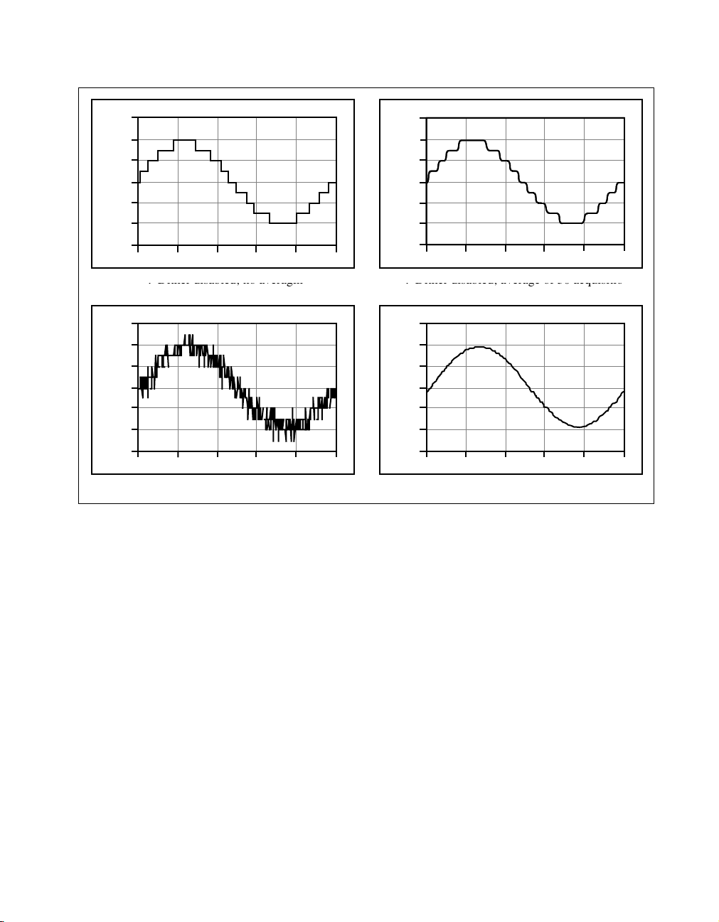
Dithering
When you enable dithering, you add approximately 0.5 LSB
rms
of white
Gaussian noise to the signal to be converted by the ADC. This addition is
useful for applications involving averaging to increase the resolution of
your device, as in calibration or spectral analysis. In such applications,
noise modulation is decreased and differential linearity is improved by the
addition of dithering. When taking DC measurements, such as when
checking the device calibration, enable dithering and average about
1,000 points to take a single reading. This process removes the effects of
quantization and reduces measurement noise, resulting in improved
resolution. For high-speed applications not involving averaging or spectral
analysis, you may want to disable dithering to reduce noise. Your software
enables and disables the dithering circuitry.
Figure 3-3 illustrates the effect of dithering on signal acquisition.
Figure 3-3a shows a small (±4 LSB) sine wave acquired with dithering off.
The ADC quantization is clearly visible. Figure 3-3b shows what happens
when 50 such acquisitions are averaged together; quantization is still
plainly visible. In Figure 3-3c, the sine wave is acquired with dithering on.
There is a considerable amount of visible noise, but averaging about 50
such acquisitions, as shown in Figure 3-3d, eliminates both the added noise
and the effects of quantization. Dithering has the effect of forcing
quantization noise to become a zero-mean random variable rather than a
deterministic function of the input signal.
6023E/6024E/6025E User Manual 3-4 ni.com
Page 24
Chapter 3 Hardware Overview
LSBs
LSBs
6.0
6.0
4.0
4.0
2.0
2.0
0.0
0.0
-2.0
-2.0
-4.0
-4.0
-6.0
-6.0
100 200 300 4000 500
100 200 300 4000 500
a. Dither disabled; no averaging b. Dither disabled; average of 50 acquisitions
a. Dither disabled; no averaging b. Dither disabled; average of 50 acquisitions
LSBs
LSBs
6.0
6.0
4.0
4.0
2.0
2.0
0.0
0.0
-2.0
-2.0
-4.0
-4.0
-6.0
-6.0
100 200 300 4000 500
100 200 300 4000 500
c. Dither enabled; no averaging
c. Dither enabled; no averaging
LSBs
LSBs
6.0
6.0
4.0
4.0
2.0
2.0
0.0
0.0
-2.0
-2.0
-4.0
-4.0
-6.0
-6.0
LSBs
LSBs
6.0
6.0
4.0
4.0
2.0
2.0
0.0
0.0
-2.0
-2.0
-4.0
-4.0
-6.0
-6.0
d. Dither enabled; average of 50 acquisitions
d. Dither enabled; average of 50 acquisitions
100 200 300 4000 500
100 200 300 4000 500
100 200 300 4000 500
100 200 300 4000 500
Figure 3-3.
Dithering
Multichannel Scanning Considerations
The devices can scan multiple channels at the same maximum rate as their
single-channel rate; however, pay careful attention to the settling times for
each of the devices. No extra settling time is necessary between channels
as long as the gain is constant and source impedances are low. Refer to
Appendix A, Specifications, for a complete listing of settling times for each
of the devices.
When scanning among channels at various gains, the settling times can
increase. When the PGIA switches to a higher gain, the signal on the
previous channel can be well outside the new, smaller range. For instance,
suppose a 4 V signal connects to channel 0 and a 1 mV signal connects to
channel 1, and suppose the PGIA is programmed to apply a gain of one to
channel 0 and a gain of 100 to channel 1. When the multiplexer switches to
channel 1 and the PGIA switches to a gain of 100, the new full-scale range
is ±50 mV.
© National Instruments Corporation 3-5 6023E/6024E/6025E User Manual
Page 25

Chapter 3 Hardware Overview
Analog Output
The approximately 4 V step from 4 V to 1 mV is 4,000% of the new
full-scale range. It can take as long as 100 µs for the circuitry to settle to
1 LSB after such a large transition. In general, this extra settling time is not
needed when the PGIA is switching to a lower gain.
Settling times can also increase when scanning high-impedance signals
due to a phenomenon called charge injection, where the analog input
multiplexer injects a small amount of charge into each signal source when
that source is selected. If the impedance of the source is not low enough,
the effect of the charge—a voltage error—has not decayed by the time the
ADC samples the signal. For this reason, keep source impedances under
1kΩ to perform high-speed scanning.
Due to the previously described limitations of settling times resulting from
these conditions, multiple-channel scanning is not recommended unless
sampling rates are low enough or it is necessary to sample several signals
as nearly simultaneously as possible. The data is much more accurate and
channel-to-channel independent if you acquire data from each channel
independently (for example, 100 points from channel 0, then 100 points
from channel 1, then 100 points from channel 2, and so on).
♦ 6025E and 6024E only
These devices supply two channels of analog output voltage at the I/O
connector. The bipolar range is fixed at ±10 V. Data written to the
digital-to-analog converter (DAC) is interpreted in two’s complement
format.
Analog Output Glitch
In normal operation, a DAC output glitches whenever it is updated with a
new value. The glitch energy differs from code to code and appears as
distortion in the frequency spectrum.
6023E/6024E/6025E User Manual 3-6 ni.com
Page 26

Digital I/O
Chapter 3 Hardware Overview
The devices contain eight lines of digital I/O (DIO<0..7>) for
general-purpose use. You can individually software-configure each line for
either input or output. At system startup and reset, the digital I/O ports are
all high impedance.
The hardware up/down control for general-purpose counters 0 and 1 are
connected onboard to DIO6 and DIO7, respectively. Thus, you can use
DIO6 and DIO7 to control the general-purpose counters. The up/down
control signals are input only and do not affect the operation of the DIO
lines.
♦ 6025E only
The 6025E device uses an 82C55A programmable peripheral interface to
provide an additional 24 lines of digital I/O that represent three 8-bit
ports—PA, PB, PC. You can program each port as an input or output port.
The 82C55A has three modes of operation—simple I/O (mode 0), strobed
I/O (mode 1), and bidirectional I/O (mode 2). In modes 1 and 2, the three
ports are divided into two groups—group A and group B. Each group has
eight data bits, plus control and status bits from Port C (PC). Modes 1 and
2 use handshaking signals from the computer to synchronize data transfers.
Refer to Chapter 4, Signal Connections, for more detailed information.
Timing Signal Routing
The DAQ-STC chip provides a flexible interface for connecting timing
signals to other devices or external circuitry. Your device uses the RTSI
bus to interconnect timing signals between devices (PCI and PXI buses
only), and the programmable function input (PFI) pins on the I/O connector
to connect the device to external circuitry. These connections are designed
to enable the device to both control and be controlled by other devices and
circuits.
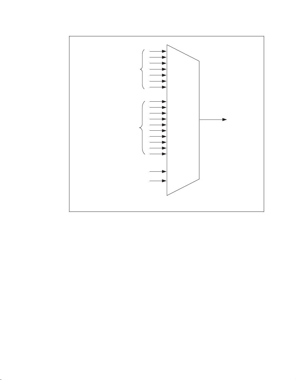
There are a total of 13 timing signals internal to the DAQ-STC that you can
control by an external source. You can also control these timing signals by
signals generated internally to the DAQ-STC, and these selections are fully
software-configurable. Figure 3-4 shows an example of the signal routing
multiplexer controlling the CONVERT* signal.
© National Instruments Corporation 3-7 6023E/6024E/6025E User Manual
Page 27
Chapter 3 Hardware Overview
†
RTSI Trigger <0..6>
PFI<0..9>
Sample Interval Counter TC
GPCTR0_OUT
CONVERT*
†
PCI and PXI Buses Only
Figure 3-4. CONVERT* Signal Routing
Figure 3-4 shows that CONVERT* can be generated from a number of
sources, including the external signals RTSI<0..6> (PCI and PXI buses
only) and PFI<0..9> and the internal signals Sample Interval Counter TC
and GPCTR0_OUT.
On PCI and PXI devices, many of these timing signals are also available as
outputs on the RTSI pins, as indicated in the RTSI Triggers sectioninthis
chapter, and on the PFI pins, as indicated in Chapter 4, Signal Connections.
Programmable Function Inputs
Ten PFI pins are available on the device connector as PFI<0..9> and
connect to the internal signal routing multiplexer of the device for each
timing signal. Software can select any one of the PFI pins as the external
source for a given timing signal. It is important to note that you can use any
of the PFI pins as an input by any of the timing signals and that multiple
timing signals can use the same PFI simultaneously. This flexible routing
6023E/6024E/6025E User Manual 3-8 ni.com
Page 28

scheme reduces the need to change physical connections to the I/O
connector for different applications.
You can also individually enable each of the PFI pins to output a specific
internal timing signal. For example, if you need the UPDATE* signal as an
output on the I/O connector, software can turn on the output driver for the
PFI5/UPDATE* pin.
Device and RTSI Clocks
♦ PCIandPXIbuses
Many device functions require a frequency timebase to generate the
necessary timing signals for controlling A/D conversions, DAC updates,
or general-purpose signals at the I/O connector.
These devices can use either its internal 20 MHz timebase or a timebase
received over the RTSI bus. In addition, if you configure the device to use
the internal timebase, you can also program the device to drive its internal
timebase over the RTSI bus to another device that is programmed to receive
this timebase signal. This clock source, whether local or from the RTSI bus,
is used directly by the device as the primary frequency source. The default
configuration at startup is to use the internal timebase without driving the
RTSI bus timebase signal. This timebase is software selectable.
Chapter 3 Hardware Overview
♦ PXI-6025E
The RTSI clock connects to other devices through the PXI trigger bus on
the PXI backplane. The RTSI clock signal uses the PXI trigger <7> line for
this connection.
RTSI Triggers
♦ PCIandPXIbuses
The seven RTSI trigger lines on the RTSI bus provide a very flexible
interconnection scheme for any device sharing the RTSI bus. These
bidirectional lines can drive any of eight timing signals onto the RTSI bus
and can receive any of these timing signals. This signal connection scheme
is shown in Figure 3-5 for PCI devices and Figure 3-6 for PXI devices.
© National Instruments Corporation 3-9 6023E/6024E/6025E User Manual
Page 29
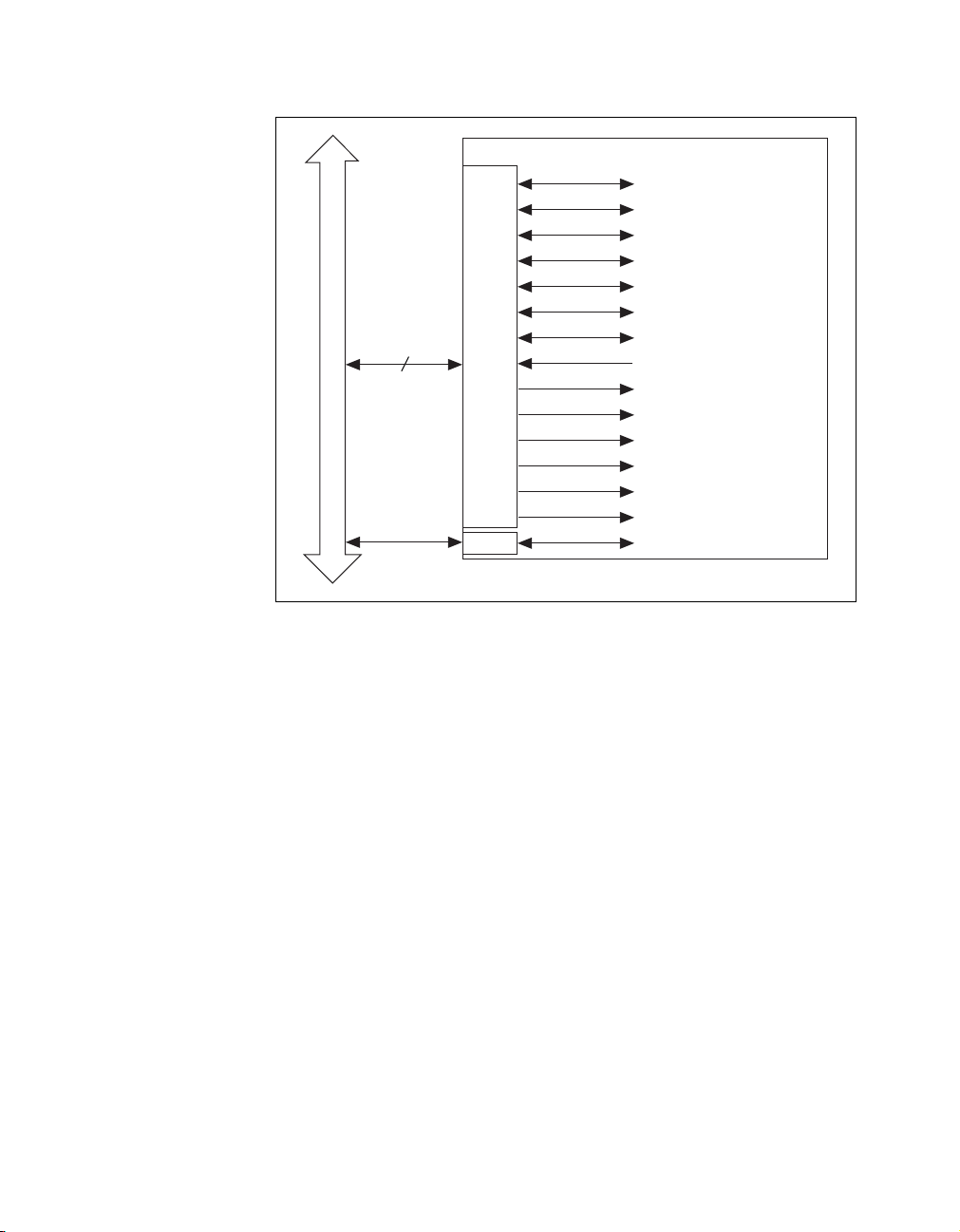
Chapter 3 Hardware Overview
Trigger
RTSI Bus Connector
Clock
DAQ-STC
TRIG1
TRIG2
CONVERT*
UPDATE*
WFTRIG
GPCTR0_SOURCE
GPCTR0_GATE
GPCTR0_OUT
7
RTSI Switch
switch
STARTSCAN
AIGATE
SISOURCE
UISOURCE
GPCTR1_SOURCE
GPCTR1_GATE
RTSI_OSC (20 MHz)
Figure 3-5. PCI RTSI Bus Signal Connection
6023E/6024E/6025E User Manual 3-10 ni.com
Page 30
PXI Star (6)
PXI Trigger (0..5)
PXI Bus Connector
PXI Trigger (7)
RTSI Switch
switch
Chapter 3 Hardware Overview
DAQ-STC
TRIG1
TRIG2
CONVERT*
UPDATE*
WFTRIG
GPCTR0_SOURCE
GPCTR0_GATE
GPCTR0_OUT
STARTSCAN
AIGATE
SISOURCE
UISOURCE
GPCTR1_SOURCE
GPCTR1_GATE
RTSI_OSC (20 MHz)
Figure 3-6. PXI RTSI Bus Signal Connection
Table 3-3 lists the name and number of pins used by the PXI-6025E.
Table 3-3.
Pins Used by PXI E Series Device
PXI E Series
Signal
PXI Pin Name PXI J2 Pin Number
RTSI<0..5> PXI Trigger<0..5> B16, A16, A17, A18, B18, C18
RTSI 6 PXI Star D17
RTSI Clock PXI Trigger 7 E16
Reserved LBL<0..3> C20, E20, A19, C19
Reserved LBR<0..12> A21, C21, D21, E21, A20,
B20, E15, A3, C3, D3, E3,
A2, B2
Refer to the Timing Connections section of Chapter 4, Signal Connections,
for a description of the signals shown in Figures 3-5 and 3-6.
© National Instruments Corporation 3-11 6023E/6024E/6025E User Manual
Page 31

Signal Connections
This chapter describes how to make input and output signal connections to
your device through the I/O connector. Table 4-1 shows the cables that can
be used with the I/O connectors to connect to different accessories.
Table 4-1. I/O Connector Details
4
Cable for
Connecting
Device with I/O
Connector
PCI-6023E,
PCI-6024E
DAQCard-6024E 68 N/A SHC68-68EP
6025E 100 SH100100
Caution
on the devices can damage the device and the computer. Maximum input ratings for each
signal are given in the Protection column of Table 4-3. National Instruments is not liable
for any damages resulting from such signal connections.
Number of
Pins
68 N/A SH6868 Shielded
Connections that exceed any of the maximum ratings of input or output signals
to 100-pin
Accessories
Shielded Cable
Cable for
Connecting
to 68-pin
Accessories
Cable,
R6868 Ribbon
Cable
Shielded Cable,
RC68-68 Ribbon
Cable
SH1006868
Shielded Cable
I/O Connector
Cable for
Connecting to
50-pin Signal
Accessories
SH6850 Shielded
Cable,
R6850 Ribbon
Cable
68M-50F
Adapter when
used with the
SHC68-68EP or
RC68-68
R1005050
Ribbon Cable
Figure 4-1 shows the pin assignments for the 68-pin I/O connector on the
PCI-6023E, PCI-6024E, and DAQCard-6024E. Figure 4-2 shows the pin
assignments for the 100-pin I/O connector on the PCI-6025E. Refer to
Appendix B, Custom Cabling and Optional Connectors, for pin
© National Instruments Corporation 4-1 6023E/6024E/6025E User Manual
Page 32

Chapter 4 Signal Connections
assignments ofthe optional 50- and 68-pin connectors. A signal description
follows the figures.
ACH8
ACH1
AIGND
ACH10
ACH3
AIGND
ACH4
AIGND
ACH13
ACH6
AIGND
ACH15
DAC0OUT
DAC1OUT
RESERVED
DIO4
DGND
DIO1
DIO6
DGND
+5 V
DGND
DGND
PFI0/TRIG1
PFI1/TRIG2
DGND
+5 V
DGND
PFI5/UPDATE*
PFI6/WFTRIG
DGND
PFI9/GPCTR0_GATE
GPCTR0_OUT
FREQ_OUT
1
1
34 68
33 67
32 66
31 65
30 64
29 63
28 62
27 61
26 60
25 59
24 58
23 57
22 56
21 55
20 54
19 53
18 52
17 51
16 50
15 49
14 48
13 47
12 46
11 45
10 44
943
842
741
640
539
438
337
236
135
ACH0
AIGND
ACH9
ACH2
AIGND
ACH11
AISENSE
ACH12
ACH5
AIGND
ACH14
ACH7
AIGND
AOGND
AOGND
DGND
DIO0
DIO5
DGND
DIO2
DIO7
DIO3
SCANCLK
EXTSTROBE*
DGND
PFI2/CONVERT*
PFI3/GPCTR1_SOURCE
PFI4/GPCTR1_GATE
GPCTR1_OUT
DGND
PFI7/STARTSCAN
PFI8/GPCTR0_SOURCE
DGND
DGND
1
Not available on the 6023E
Figure 4-1. I/O Connector Pin Assignment for the 6023E/6024E
6023E/6024E/6025E User Manual 4-2 ni.com
Page 33

Chapter 4 Signal Connections
AIGND PC7
AIGND GND
ACH0 PC6
ACH8 GND
ACH1 PC5
ACH9 GND
ACH2 PC4
ACH10 GND
ACH3 PC3
ACH11 GND
ACH4 PC2
ACH12 GND
ACH5 PC1
ACH13 GND
ACH6 PC0
ACH14 GND
ACH7 PB7
ACH15 GND
AISENSE PB6
DAC0OUT GND
DAC1OUT PB5
RESERVED GND
AOGND PB4
DGND GND
DIO0 PB3
DIO4 GND
DIO1 PB2
DIO5 GND
DIO2 PB1
DIO6 GND
DIO3 PB0
DIO7 GND
DGND PA7
SCANCLK GND
EXTSTROBE* PA5
PFI0/TRIG1 GND
PFI1/TRIG2 PA4
PFI2/CONVERT* GND
PFI3/GPCTR1_SOURCE PA3
PFI4/GPCTR1_GATE GND
GPCTR1_OUT PA2
PFI5/UPDATE* GND
PFI6/WFTRIG PA1
PFI7/STARTSCAN GND
PFI8/GPCTR0_SOURCE PA0
PFI9/GPCTR0_GATE GND
GPCTR0_OUT +5 V
FREQ_OUT GND
151
252
353
454
555
656
757
858
959
10 60
11 61
12 62
13 63
14 64
15 65
16 66
17 67
18 68
19 69
20 70
21 71
22 72
23 73
24 74
25 75
26 76
27 77
28 78
29 79
30 80
31 81
32 82
33 83
34 84
+5 V GND
35 85
+5 V PA6
36 86
37 87
38 88
39 89
40 90
41 91
42 92
43 93
44 94
45 95
46 96
47 97
48 98
49 99
50 100
Figure 4-2. I/O Connector Pin Assignment for the 6025E
© National Instruments Corporation 4-3 6023E/6024E/6025E User Manual
Page 34

Chapter 4 Signal Connections
Table 4-2 shows the I/O connector signal descriptions for the 6023E,
6024E, and 6025E.
Table 4-2. I/O Connector Signal Descriptions
Signal Name Reference Direction Description
AIGND — — Analog input ground—these pins are the reference point for
single-ended measurements in RSE configuration and the
bias current return point for DIFF measurements. All three
ground references—AIGND, AOGND, and DGND—are
connected on your device.
ACH<0..15> AIGND Input Analog input channels 0 through 15—you can configure
each channel pair, ACH<i, i+8> (i = 0..7), as either one
DIFF input or two single-ended inputs.
AISENSE AIGND Input Analog input sense—this pin serves as the reference node
for any of channels ACH <0..15> in NRSE configuration.
DAC0OUT
1
AOGND Output Analog channel 0 output—this pin supplies the voltage
output of analog output channel 0.
DAC1OUT
1
AOGND Output Analog channel 1 output—this pin supplies the voltage
output of analog output channel 1.
AOGND — — Analog output ground—the analog output voltages are
referenced to this node. All three ground
references—AIGND, AOGND, andDGND—are connected
together on your device.
DGND — — Digital ground—this pin supplies the reference for the
digital signals at the I/O connector as well as the +5 VDC
supply. All three ground references—AIGND, AOGND,
and DGND—are connected on your device.
DIO<0..7> DGND Input or
Output
2
PA <0 . . 7>
DGND Input or
Output
Digital I/O signals—DIO6 and 7 can control the up/down
signal of general-purpose counters 0 and 1, respectively.
Port A bidirectional digital data lines for the 82C55A
programmable peripheral interface on the 6025E. PA7
is the MSB. PA0 is the LSB.
PB<0..7>
2
DGND Input or
Output
Port B bidirectional digital data lines for the 82C55A
programmable peripheral interface on the 6025E. PB7
is the MSB. PB0 is the LSB.
PC<0..7>
2
DGND Input or
Output
Port C bidirectional digital data lines for the 82C55A
programmable peripheral interface on the 6025E. PC7
is the MSB. PC0 is the LSB.
+5 V DGND Output +5 VDC Source—these pins are fused for up to 1 A of
+5 V supply on the PCI and PXI devices, or up to 0.75 A
from a DAQCard device. The fuse is self-resetting.
6023E/6024E/6025E User Manual 4-4 ni.com
Page 35

Chapter 4 Signal Connections
Table 4-2. I/O Connector Signal Descriptions (Continued)
Signal Name Reference Direction Description
SCANCLK DGND Output scan clock—this pin pulses once for each A/D conversion
in scanning mode when enabled. The low-to-high edge
indicates when the input signal can be removed from the
input or switched to another signal.
EXTSTROBE* DGND Output External strobe—you can toggle this output under software
PFI0/TRIG1 DGND Input
Output
PFI1/TRIG2 DGND Input
Output
PFI2/CONVERT* DGND Input
Output
PFI3/GPCTR1_SOURCE DGND Input
Output
PFI4/GPCTR1_GATE DGND Input
control to latch signals or trigger events on external devices.
PFI0/Trigger 1—as an input, this is one of the
programmable function inputs (PFIs). PFI signals are
explained in the Timing Connections sectioninthischapter.
As an output, this is the TRIG1 (AI start trigger) signal.
In posttrigger data acquisition sequences, a low-to-high
transition indicates the initiation of the acquisition
sequence. In pretrigger applications, a low-to-high
transition indicates the initiation of the pretrigger
conversions.
PFI1/Trigger 2—as an input, this is one of the PFIs.
As an output, this is the TRIG2 (AI stop trigger) signal. In
pretrigger applications, a low-to-high transition indicates
the initiation of the posttrigger conversions. TRIG2 is not
used in posttrigger applications.
PFI2/Convert—as an input, this is one of the PFIs.
As an output, this is the CONVERT* (AI convert) signal.
A high-to-low edge on CONVERT* indicates that an A/D
conversion is occurring.
PFI3/Counter 1 Source—as an input, this is one of the PFIs.
As an output, this is the GPCTR1_SOURCE signal. This
signal reflects the actual source connected to the
general-purpose counter 1.
PFI4/Counter 1 Gate—as an input, this is one of the PFIs.
Output
GPCTR1_OUT DGND Output Counter 1 Output—this output is from the general-purpose
© National Instruments Corporation 4-5 6023E/6024E/6025E User Manual
As an output, this is the GPCTR1_GATE signal. This signal
reflects the actual gate signal connected to the
general-purpose counter 1.
counter 1 output.
Page 36

Chapter 4 Signal Connections
Table 4-2. I/O Connector Signal Descriptions (Continued)
Signal Name Reference Direction Description
PFI5/UPDATE* DGND Input
PFI5/Update—as an input, this is one of the PFIs.
Output
As an output, this is the UPDATE* (AO Update) signal. A
high-to-low edge on UPDATE* indicates that the analog
output primary group is being updated for the 6024E or
6025E.
PFI6/WFTRIG DGND Input
PFI6/Waveform Trigger—as an input, this is one of the
PFIs.
Output
As an output, this is the WFTRIG (AO Start Trigger) signal.
In timed analog output sequences, a low-to-high transition
indicates the initiation of the waveform generation.
PFI7/STARTSCAN DGND Input
Output
PFI7/Start of Scan—as an input, this is one of the PFIs.
As an output, this is the STARTSCAN (AI Scan Start)
signal. This pin pulses once at the start of each analog input
scan in the interval scan. A low-to-high transition indicates
the start of the scan.
PFI8/GPCTR0_SOURCE DGND Input
PFI8/Counter 0 Source—as an input, this is one of the
PFIs.
Output
As an output, this is the GPCTR0_SOURCE signal.
This signal reflects the actual source connected to the
general-purpose counter 0.
PFI9/GPCTR0_GATE DGND Input
Output
PFI9/Counter 0 Gate—as an input, this is one of the PFIs.
As an output, this is the GPCTR0_GATE signal. This signal
reflects the actual gate signal connected to the
general-purpose counter 0.
GPCTR0_OUT DGND Output Counter 0 Output—this output is from the general-purpose
counter 0 output.
FREQ_OUT DGND Output Frequency Output—this output is from the frequency
generator output.
*
Indicates that the signal is active low
1
Not available on the 6023E
2
Not available on the 6023E or 6024E
6023E/6024E/6025E User Manual 4-6 ni.com
Page 37

Chapter 4 Signal Connections
Table 4-3 shows the I/O signal summary for the 6023E, 6024E, and 6025E.
Table 4-3. I/O Signal Summary
Signal
Signal Name
Typ e a nd
Direction
ACH<0..15> AI 100 GΩ
Impedance
Input/
Output
Protection
(Volts)
On/Off
Source
(mA at V)
Sink
(mA
at V)
Rise
Time
(ns)
Bias
42/35 — — — ±200 pA
in
parallel
with
100 pF
AISENSE AI 100 GΩ
40/25 — — — ±200 pA
in
parallel
with
100 pF
AIGND AO — — — — — —
DAC0OUT
(6024E and 6025E only)
DAC1OUT
(6024E and 6025E only)
AO 0.1 Ω Short-circuit
to ground
AO 0.1 Ω Short-circuit
to ground
5at10 5at-10 10
V/µs
5at10 5at-10 10
V/µs
—
—
AOGND AO — — — — — —
DGND DO — — — — — —
VCC DO 0.1 Ω Short-circuit
1A fused — — —
to ground
DIO<0..7> DIO — Vcc+0.5 13 at (Vcc-0.4) 24 at
1.1 50 kΩ pu
0.4
PA <0 . . 7>
(6025E only)
PB<0..7>
(6025E only)
PC<0..7>
(6025E only)
DIO — Vcc+0.5 2.5 at 3.7min 2.5 at
0.4
DIO — Vcc+0.5 2.5 at 3.7min 2.5 at
0.4
DIO — Vcc+0.5 2.5 at 3.7min 2.5 at
0.4
5 100 kΩ
pu
5 100 kΩ
pu
5 100 kΩ
pu
SCANCLK DO — — 3.5 at (Vcc-0.4) 5at0.4 1.5 50 kΩ pu
EXTSTROBE* DO — — 3.5 at (Vcc-0.4) 5at0.4 1.5 50 kΩ pu
PFI0/TRIG1 DIO — Vcc+0.5 3.5 at (Vcc-0.4) 5at0.4 1.5 50 kΩ pu
PFI1/TRIG2 DIO — Vcc+0.5 3.5 at (Vcc-0.4) 5at0.4 1.5 50 kΩ pu
PFI2/CONVERT* DIO — Vcc+0.5 3.5 at (Vcc-0.4) 5at0.4 1.5 50 kΩ pu
PFI3/GPCTR1_SOURCE DIO — Vcc+0.5 3.5 at (Vcc-0.4) 5at0.4 1.5 50 kΩ pu
© National Instruments Corporation 4-7 6023E/6024E/6025E User Manual
Page 38

Chapter 4 Signal Connections
Table 4-3. I/O Signal Summary (Continued)
Signal
Signal Name
PFI4/GPCTR1_GATE DIO — Vcc+0.5 3.5 at (Vcc-0.4) 5at0.4 1.5 50 kΩ pu
GPCTR1_OUT DO — — 3.5 at (Vcc-0.4) 5at0.4 1.5 50 kΩ pu
PFI5/UPDATE* DIO — Vcc+0.5 3.5 at (Vcc-0.4) 5at0.4 1.5 50 kΩ pu
PFI6/WFTRIG DIO — Vcc+0.5 3.5 at (Vcc-0.4) 5at0.4 1.5 50 kΩ pu
PFI7/STARTSCAN DIO — Vcc+0.5 3.5 at (Vcc-0.4) 5at0.4 1.5 50 kΩ pu
PFI8/GPCTR0_SOURCE DIO — Vcc+0.5 3.5 at (Vcc-0.4) 5at0.4 1.5 50 kΩ pu
PFI9/GPCTR0_GATE DIO — Vcc+0.5 3.5 at (Vcc-0.4) 5at0.4 1.5 50 kΩ pu
GPCTR0_OUT DO — — 3.5 at (Vcc-0.4) 5at0.4 1.5 50 kΩ pu
FREQ_OUT DO — — 3.5 at (Vcc-0.4) 5at0.4 1.5 50 kΩ pu
AI = Analog Input DIO = Digital Input/Output pu = pullup
AO = Analog Output DO = Digital Output
Note: The tolerance on the 50 kΩ pullup and pulldown resistors is very large. Actual value can range between 17 kΩ and
100 kΩ.
Typ e a nd
Direction
Impedance
Input/
Output
Protection
(Volts)
On/Off
Source
(mA at V)
Sink
(mA
at V)
Rise
Time
(ns)
Bias
Analog Input Signal Overview
The analog input signals for these devices are ACH<0..15>, ASENSE, and
AIGND. Connection of these analog input signals to your device depends
on the type of input signal source and the configuration of the analog input
channels you are using. This section provides an overview of the different
types of signal sources and analog input configuration modes. More
specific signal connection information is provided in the Analog Input
Signal Connections section.
Types of Signal Sources
When configuring the input channels and making signal connections,
you must first determine whether the signal sources are floating or
ground-referenced.
6023E/6024E/6025E User Manual 4-8 ni.com
Page 39

Chapter 4 Signal Connections
Floating Signal Sources
A floating signal source is not connected in any way to the building ground
system, but has an isolated ground-reference point. Some examples of
floating signal sources are outputs of transformers, thermocouples,
battery-powered devices, optical isolators, and isolation amplifiers. An
instrument or device that has an isolated output is a floating signal source.
You must tie the ground reference of a floating signal to the analog input
ground of your device to establish a local or onboard reference for the
signal. Otherwise, the measured input signal varies as the source floats out
of the common-mode input range.
Ground-Referenced Signal Sources
A ground-referenced signal source is connected in some way to the
building system ground and is, therefore, already connected to a common
ground point with respect to the device, assuming that the computer is
plugged into the same power system. Non-isolated outputs of instruments
and devices that plug into the building power system fall into this category.
The difference in ground potential between two instruments connected to
the same building power system is typically between 1 and 100 mV, but can
be much higher if power distribution circuits are not properly connected.
If a grounded signal source is improperly measured, this difference can
appear as an error in the measurement. The connection instructions for
grounded signal sources are designed to eliminate this ground potential
difference from the measured signal.
Analog Input Modes
You can configure your device for one of three input
modes—nonreferenced single ended (NRSE), referenced single ended
(RSE), and differential (DIFF). With the different configurations, you can
use the PGIA in different ways. Figure 4-3 shows a diagram of the PGIA
of your device.
© National Instruments Corporation 4-9 6023E/6024E/6025E User Manual
Page 40

Chapter 4 Signal Connections
Programmable
Gain
V
in+
+
Instrumentation
Amplifier
V
m
+
Measured
Voltage
PGIA
V
in-
-
-
Vm=[V
Figure 4-3. Programmable Gain Instrumentation Amplifier (PGIA)
In single-ended mode (RSE and NRSE), signals connected to ACH<0..15>
are routed to the positive input of the PGIA. In DIFF mode, signals
connected to ACH<0..7> are routed to the positive input of the PGIA, and
signals connected to ACH<8..15> are routed to the negative input of the
PGIA.
Caution
Exceeding the DIFF and common-mode input ranges distorts your input signals.
Exceeding the maximum input voltage rating can damage the device and the computer.
National Instruments is not liable for any damages resulting from such signal connections.
The maximum input voltage ratings are listed in the Protection column of Table 4-3.
in+-Vin-
]* Gain
In NRSE mode, the AISENSE signal connects internally to the negative
input of the PGIA when their corresponding channels are selected. In DIFF
and RSE modes, AISENSE is left unconnected.
AIGND is an analog input common signal that routes directly to the ground
connection point on the devices. You can use this signal for a general analog
ground connection point to your device if necessary.
The PGIA applies gain and common-mode voltage rejection and presents
high input impedance to the analog input signals connected to your device.
Signals are routed to the positive and negative inputs of the PGIA through
input multiplexers on the device. The PGIA converts two input signals to a
signal that is the difference between the two input signals multiplied by the
6023E/6024E/6025E User Manual 4-10 ni.com
Page 41

gain setting of the amplifier. The amplifier output voltage is referenced to
the ground for the device. The A/D converter (ADC) of your device
measures this output voltage when it performs A/D conversions.
Reference all signals to ground either at the source device or at the device.
If you have a floating source, reference the signal to ground by using the
RSE input mode or the DIFF input configuration with bias resistors (see the
Differential Connections for Nonreferenced or Floating Signal Sources
section). If you have a grounded source, do not reference the signal to
AIGND. You can avoid this reference by using DIFF or NRSE input
configurations.
Analog Input Signal Connections
The following sections discuss the use of single-ended and DIFF
measurements and recommendations for measuring both floating and
ground-referenced signal sources.
Figure 4-4 summarizes the recommended input configuration for both
types of signal sources.
Chapter 4 Signal Connections
© National Instruments Corporation 4-11 6023E/6024E/6025E User Manual
Page 42

Chapter 4 Signal Connections
Signal Source Type
Input
Differential
(DIFF)
Single-Ended —
Ground
Referenced
(RSE)
Floating Signal Source
(Not Connected to Building Ground)
Examples
• Ungrounded Thermocouples
• Signal conditioning with isolated outputs
• Battery devices
+
V1
-
ACH(+)
ACH (-)
R
+
-
AIGND
See text for information on bias resistors.
+
V1
-
ACH
AIGND
+
-
Grounded Signal Source
Examples
• Plug-in instruments with
nonisolated outputs
+
V1
-
NOT RECOMMENDED
+
V1
-
+Vg -
ACH(+)
ACH (-)
ACH
+
-
AIGND
+
-
Ground-loop losses, Vg, are added to
measured signal
Single-Ended —
Nonreferenced
(NRSE)
+
V1
-
ACH
AISENSE
+
-
R
AIGND
+
V1
-
ACH
AISENSE
+
-
AIGND
See text for information on bias resistors.
Figure 4-4. Summary of Analog Input Connections
6023E/6024E/6025E User Manual 4-12 ni.com
Page 43

Chapter 4 Signal Connections
Differential Connection Considerations (DIFF Input Configuration)
A DIFF connection is one in which the analog input signal has its own
reference signal or signal return path. These connections are available
when the selected channel is configured in DIFF input mode. The input
signal is connected to the positive input of the PGIA, and its reference
signal, or return, is connected to the negative input of the PGIA.
When you configure a channel for DIFF input, each signal uses two
multiplexer inputs—one for the signal and one for its reference signal.
Therefore, with a DIFF configuration for every channel, up to eight analog
input channels are available.
Use DIFF input connections for any channel that meets any of the following
conditions:
• The input signal is low level (less than 1 V).
• The leads connecting the signal to the device are greater than
3m(10ft).
• The input signal requires a separate ground-reference point or return
signal.
• The signal leads travel through noisy environments.
DIFF signal connections reduce picked up noise and increase
common-mode noise rejection. DIFF signal connections also allow input
signals to float within the common-mode limits of the PGIA.
© National Instruments Corporation 4-13 6023E/6024E/6025E User Manual
Page 44

Chapter 4 Signal Connections
Ground-
Referenced
Signal
Source
+
V
s
–
Differential Connections for Ground-Referenced
Signal Sources
Figure 4-5 shows how to connect a ground-referenced signal source to a
channel on the device configured in DIFF input mode.
ACH+
Programmable Gain
Instrumentation
+
Amplifier
Common-
Mode
Noise and
Ground
Potential
I/O Connector
PGIA
ACH–
+
V
cm
–
Input Multiplexers
AISENSE
AIGND
Selected Channel in DIFF Configuration
–
+
m
Measured
Voltage
–
V
Figure 4-5. Differential Input Connections for Ground-Referenced Signals
With this type of connection, the PGIA rejects both the common-mode
noise in the signal and the ground potential difference between the signal
source and the device ground, shown as V
in Figure 4-5.
cm
6023E/6024E/6025E User Manual 4-14 ni.com
Page 45

Floating
Signal
Source
Chapter 4 Signal Connections
Differential Connections for Nonreferenced or Floating Signal Sources
Figure 4-6 shows how to connect a floating signal source to a channel
configured in DIFF input mode.
ACH+
Bias
resistors
(see text)
+
V
s
–
Programmable Gain
Instrumentation
Amplifier
+
Bias
Current
Return
Paths
I/O Connector
PGIA
ACH–
–
Input Multiplexers
AISENSE
AIGND
Selected Channel in DIFF Configuration
+
m
Measured
Voltage
–
V
Figure 4-6. Differential Input Connections for Nonreferenced Signals
Figure 4-6 shows two bias resistors connected in parallel with the signal
leads of a floating signal source. If you do not use the resistors and the
source is truly floating, the source is not likely to remain within the
common-mode signal range of the PGIA. The PGIA then saturates, causing
erroneous readings.
© National Instruments Corporation 4-15 6023E/6024E/6025E User Manual
Page 46

Chapter 4 Signal Connections
You must reference the source to AIGND. The easiest way is to connect the
positive side of the signal to the positive input of the PGIA and connect the
negative side of the signal to AIGND as well as to the negative input of the
PGIA, without any resistors at all. This connection works well for
DC-coupled sources with low source impedance (less than 100 Ω).
However, for larger source impedances, this connection leaves the DIFF
signal path significantly out of balance. Noise that couples electrostatically
onto the positive line does not couple onto the negative line because it is
connected to ground. Hence, this noise appears as a DIFF-mode signal
instead of a common-mode signal, and the PGIA does not reject it. In this
case, instead of directly connecting the negative line to AIGND, connect it
to AIGND through a resistor that is about 100 times the equivalent source
impedance. The resistor puts the signal path nearly in balance, so that about
the same amount of noise couples onto both connections, yielding better
rejection of electrostatically coupled noise. Also, this configuration does
not load down the source (other than the very high input impedance of the
PGIA).
You can fully balance the signal path by connecting another resistor of the
same value between the positive input and AIGND, as shown in Figure 4-6.
This fully balanced configuration offers slightly better noise rejection but
has the disadvantage of loading the source down with the series
combination (sum) of the two resistors. If, for example, the source
impedance is 2 kΩ and each of the two resistors is 100 kΩ, the resistors
load down the source with 200 kΩ and produce a –1% gain error.
Both inputs of the PGIA require a DC path to ground in order for the PGIA
to work. If the source is AC coupled (capacitively coupled), the PGIA needs
a resistor between the positive input and AIGND. If the source has low
impedance, choose a resistor that is large enough not to significantly load
the source but small enough not to produce significant input offset voltage
as a result of input bias current (typically 100 kΩ to1MΩ). In this case,
you can tie the negative input directly to AIGND. If the source has high
output impedance, balance the signal path as previously described using the
same value resistor on both the positive and negative inputs; be aware that
there is some gain error from loading down the source.
6023E/6024E/6025E User Manual 4-16 ni.com
Page 47

Single-Ended Connection Considerations
A single-ended connection is one in which the device analog input signal is
referenced to a ground that it can share with other input signals. The input
signal is tied to the positive input of the PGIA, and the ground is tied to the
negative input of the PGIA.
When every channel is configured for single-ended input, up to 16 analog
input channels are available.
You can use single-ended input connections for any input signal that meets
the following conditions:
• The input signal is high level (greater than 1 V).
• The leads connecting the signal to the device are less than 10 ft (3 m).
• The input signal can share a common reference point with other
signals.
DIFF input connections are recommended for greater signal integrity for
any input signal that does not meet the preceding conditions.
Using your software, you can configure the channels for two different types
of single-ended connections—RSE configuration and NRSE configuration.
The RSE configuration is used for floating signal sources; in this case, the
device provides the reference ground point for the external signal. The
NRSE input configuration is used for ground-referenced signal sources; in
this case, the external signal supplies its own reference ground point and the
device should not supply one.
Chapter 4 Signal Connections
In single-ended configurations, more electrostatic and magnetic noise
couples into the signal connections than in DIFF configurations. The
coupling is the result of differences in the signal path. Magnetic coupling
is proportional to the area between the two signal conductors. Electrical
coupling is a function of how much the electric field differs between the
two conductors.
© National Instruments Corporation 4-17 6023E/6024E/6025E User Manual
Page 48

Chapter 4 Signal Connections
Single-Ended Connections for Floating Signal
Sources (RSE Configuration)
Figure 4-7 shows how to connect a floating signal source to a channel
configured for RSE mode.
ACH
Floating
Signal
Source
+
V
s
–
I/O Connector
Programmable Gain
Instrumentation Amplifier
+
Input Multiplexers
AISENSE
AIGND
Selected Channel in RSE Configuration
Figure 4-7. Single-Ended Input Connections for Nonreferenced or Floating Signals
PGIA
–
V
m
+
Measured
Voltage
–
Single-Ended Connections for Grounded Signal
Sources (NRSE Configuration)
To measure a grounded signal source with a single-ended configuration,
you must configure your device in the NRSE input configuration. Connect
the signal to the positive input of the PGIA, and connect the signal local
ground reference to the negative input of the PGIA. The ground point of the
signal, therefore, connects to the AISENSE pin. Any potential difference
between the device ground and the signal ground appears as a
common-mode signal at both the positive and negative inputs of the PGIA,
and this difference is rejected by the amplifier. If the input circuitry of a
device were referenced to ground, in this situation as in the RSE input
configuration, this difference in ground potentials appears as an error in the
measured voltage.
6023E/6024E/6025E User Manual 4-18 ni.com
Page 49

Chapter 4 Signal Connections
Figure 4-8 shows how to connect a grounded signal source to a channel
configured for NRSE mode.
ACH<0..15>
Ground-
Referenced
Signal
Source
Common-
Mode
Noise
and Ground
Potential
+
V
s
–
+
V
cm
–
I/O Connector
Figure 4-8.
+
Input Multiplexers
AIGND
Selected Channel in NRSE Configuration
AISENSE
–
Single-Ended Input Connections for Ground-Referenced Signals
Common-Mode Signal Rejection Considerations
Figures 4-5 and 4-8 show connections for signal sources that are already
referenced to some ground point with respect to the device. In these cases,
the PGIA can reject any voltage caused by ground potential differences
between the signal source and the device. In addition, with DIFF input
connections, the PGIA can reject common-mode noise pickup in the leads
connecting the signal sources to the device. The PGIA can reject
common-mode signals as long as V+
within ±11 V of AIGND.
and V–in(input signals) are both
in
Instrumentation
Amplifier
PGIA
+
m
Measured
Voltage
–
V
Analog Output Signal Connections
♦ 6024E and 6025E
The analog output signals are DAC0OUT, DAC1OUT, and AOGND.
DAC0OUT and DAC1OUT are not available on the 6023E. DAC0OUT is
the voltage output signal for analog output channel 0. DAC1OUT is the
voltage output signal for analog output channel 1.
© National Instruments Corporation 4-19 6023E/6024E/6025E User Manual
Page 50

Chapter 4 Signal Connections
Load
AOGND is the ground reference signal for both analog output channels and
the external reference signal. Figure 4-9 shows how to make analog output
connections to your device.
DAC0OUT
Channel 0
VOUT 0
+
–
–
AOGND
Load
I/O Connector
VOUT 1
+
DAC1OUT
Figure 4-9. Analog Output Connections
Digital I/O Signal Connections
All Devices
All devices have digital I/O signals DIO<0..7> and DGND. DIO<0..7> are
the signals making up the DIO port, and DGND is the ground-reference
signal for the DIO port. You can program all lines individually as inputs or
outputs. Figure 4-10 shows signal connections for three typical digital I/O
applications.
Caution
damage the DAQ device and the computer. National Instruments is not liable for any
damages resulting from such signal connections.
Exceeding the maximum input voltage ratings, which are listed in Table 4-2, can
Channel 1
Analog Output Channels
6023E/6024E/6025E User Manual 4-20 ni.com
Page 51

LED
Chapter 4 Signal Connections
+5 V
DIO<4..7>
+5 V
TTL Signal
DIO<0..3>
Switch
DGND
I/O Connector
Figure 4-10. Digital I/O Connections
Figure 4-10 shows DIO<0..3> configured for digital input and DIO<4..7>
configured for digital output. Digital input applications include receiving
TTL signals and sensing external device states such as the state of the
switch shown in the Figure 4-11. Digital output applications include
sending TTL signals and driving external devices such as the LED shown
in Figure 4-11. Figure 4-11 depicts signal connections for three typical
digital I/O applications.
© National Instruments Corporation 4-21 6023E/6024E/6025E User Manual
Page 52

Chapter 4 Signal Connections
+5 V
LED
Por t A
PA<3..0>
Por t B
PB<7..4>
DIO Device
+5 V
Switch
I/O Connector
TTL Signal
GND
Figure 4-11. Digital I/O Connections Block Diagram
Programmable Peripheral Interface (PPI)
♦ 6025E only
The 6025E device uses an 82C55A PPI to provide an additional 24 lines
of digital I/O that represent three 8-bit ports—PA, PB, and PC. You can
program each port as an input or output port.
In Figure 4-11, port A of one PPI is configured for digital output, and
port B is configured for digital input. Digital input applications include
receiving TTL signals and sensing external device states such as the state
of the switch in Figure 4-11. Digital output applications include sending
6023E/6024E/6025E User Manual 4-22 ni.com
Page 53

TTL signals and driving external devices such as the LED shown in
Figure 4-11.
Port C Pin Assignments
♦ 6025 only
The signals assigned to port C depend on how the 82C55A is configured.
In mode 0, or no handshaking configuration, port C is configured as two
4-bit I/O ports. In modes 1 and 2, or handshaking configuration, port C
is used for status and handshaking signals with any leftover lines available
for general-purpose I/O. Table 4-4 summarizes the port C signal
assignments for each configuration. You can also use ports A and B in
different modes; the table does not show every possible combination.
Note
Table 4-4 shows both the port C signal assignments and the terminology
correlation between different documentation sources. The 82C55A terminology refers
to the different 82C55A configurations as modes, whereas NI-DAQ, ComponentWorks,
LabWindows/CVI, and LabVIEW documentation refers to them as handshaking and no
handshaking.
Chapter 4 Signal Connections
Table 4-4. Port C Signal Assignments
Configuration Terminology Signal Assignments
6023E/
6024E/6025E
User Manual
Mode 0
(Basic I/O)
Mode 1
(Strobed Input)
Mode 1
(Strobed Output)
Mode 2
(Bidirectional
Bus)
* Indicates that the signal is active low.
Subscripts A and B denote port A or port B handshaking signals.
© National Instruments Corporation 4-23 6023E/6024E/6025E User Manual
National
Instruments
Software
No
Handshaking
Handshaking
Handshaking
Handshaking
PC7 PC6 PC5 PC4 PC3 PC2 PC1 PC0
I/O I/O I/O I/O I/O I/O I/O I/O
I/O I/O IBF
OBFA* ACKA* I/O I/O INTRAACKB* OBFB* INTR
OBFA* ACKA* IBF
STBA* INTRASTBB* IBFBBINTR
A
A
STBA* INTR
I/O I/O I/O
A
B
B
Page 54

Chapter 4 Signal Connections
Power-up State
♦ 6025E only
The 6025E contains bias resistors that control the state of the digital I/O
lines PA<0..7>,PB<0..7>,PC<0..7> at power up. Each digital I/O line is
configured as an input, pulled high by a 100 kΩ bias resistor.
You can change individual lines from pulled up to pulled down by adding
your own external resistors. This section describes the procedure.
Changing DIO Power-up State to Pulled Low
Each DIO line is pulled to Vcc(approximately +5 VDC) with a 100 kΩ
resistor. To pull a specific line low, connect between that line and ground
a pull-down resistor (R
The DIO lines provide a maximum of 2.5 mA at 3.7 V in the high state.
Using the largest possible resistor ensures that you do not use more current
than necessary to perform the pull-down task.
However, make sure the value of the resistor is not so large that leakage
current from the DIO line along with the current from the 100 kΩ pull-up
resistor drives the voltage at the resistor above a TTL-low level of 0.4 VDC.
Figure 4-12 shows the DIO configuration for high DIO power-up state.
) whose value gives you a maximum of 0.4 VDC.
L
100 k
+5 V
GND
Digital I/O Line
R
L
Device
82C55
Figure 4-12. DIO Channel Configured for High DIO Power-up Statewith ExternalLoad
Example
A given DIO line is pulled high at power up. To pull it low on power up with
an external resistor, follow these steps:
1. Install a load (R
). Remember that the smaller the resistance, the
L
greater the current consumption and the lower the voltage.
6023E/6024E/6025E User Manual 4-24 ni.com
Page 55

2. Using the following formula, calculate the largest possible load to
This resistor value, 7.1 kΩ, provides a maximum of 0.4 V on the DIO line
at power up. You can substitute smaller resistor values to lower the voltage
or to provide a margin for V
smaller values draw more current, leaving less drive current for other
circuitry connected to this line. The 7.1 kΩ resistor reduces the amount of
logic high source current by 0.4 mA with a 2.8 V output.
Timing Specifications
♦ 6025E only
Chapter 4 Signal Connections
maintain a logic low level of 0.4 V and supply the maximum driving
current:
V = I × RL ⇒ RL = V/I
where:
V = 0.4 V Voltage across RL
I =46µA+10µA 4.6 V across the 100 kΩ pull-up resistor
and 10 µA maximum leakage current
Therefore:
RL =7.1kΩ ;0.4V/56µA
variations and other factors. However,
cc
This section lists the timing specifications for handshaking with your
6025E PC<0..7> lines. The handshaking lines STB* and IBF synchronize
input transfers. The handshaking lines OBF* and ACK* synchronize
output transfers. Table 4-5 describes signals appearing in the handshaking
diagrams.
Table 4-5. Signal Names Used in Timing Diagrams
Name Ty pe Description
STB* Input Strobe input—a low signal on this handshaking line loads data into
the input latch.
IBF Output Input buffer full—a high signal on this handshaking line indicates
that data has been loaded into the input latch. A low signal indicates
the device is ready for more data. This is an input acknowledge
signal.
© National Instruments Corporation 4-25 6023E/6024E/6025E User Manual
Page 56

Chapter 4 Signal Connections
Table 4-5. Signal Names Used in Timing Diagrams (Continued)
Name Ty pe Description
ACK* Input Acknowledge input—a low signal on this handshaking line
indicates that the data written to the port has been accepted. This
signal is a response from the external device indicating that it has
received the data from your DIO device.
OBF* Output Output buffer full—a low signal on this handshaking line indicates
that data has been written to the port.
INTR Output Interrupt request—this signal becomes high when the 82C55A
requests service during a data transfer. You must set the appropriate
interrupt enable bits to generate this signal.
RD* Internal Read—this signal is the read signal generated from the control lines
of the computer I/O expansion bus.
WR* Internal Write—this signal is the write signal generated from the control
lines of the computer I/O expansion bus.
DATA Bidirectional Data lines at the specified port—for output mode, this signal
indicates the availability of data on the data line. For input mode,
this signal indicates when the data on the data lines should be valid.
6023E/6024E/6025E User Manual 4-26 ni.com
Page 57

Mode 1 Input Timing
Timing specifications for an input transfer in mode 1 are shown in
Figure 4-13.
Chapter 4 Signal Connections
T1
T2
STB *
IBF
INTR
RD *
T3
DATA
T4
T7
T6
T5
Name Description Minimum Maximum
T1
T2
T3
T4
T5
T6
T7
All timing values are in nanoseconds.
STB* Pulse Width
STB* = 0 to IBF = 1
Data before STB* = 1
STB*=1toINTR=1
Data after STB* = 1
RD*=0toINTR=0
RD*=1toIBF=0
100 —
— 150
20 —
— 150
50 —
— 200
— 150
Figure 4-13. Timing Specifications for Mode 1 Input Transfer
© National Instruments Corporation 4-27 6023E/6024E/6025E User Manual
Page 58

Chapter 4 Signal Connections
Mode 1 Output Timing
Timing specifications for an output transfer in mode 1 are shown in
Figure 4-14.
WR*
OBF*
INTR
ACK*
DATA
T3
T4
T1
T5
T2
T6
Name Description Minimum Maximum
T1
T2
T3
T4
T5
T6
All timing values are in nanoseconds.
WR*=0toINTR=0
WR*=1toOutput
WR*=1toOBF*=0
ACK* = 0 to OBF* = 1
ACK* Pulse Width
ACK* = 1 to INTR = 1
Figure 4-14. Timing Specifications for Mode 1 Output Transfer
6023E/6024E/6025E User Manual 4-28 ni.com
— 250
— 200
— 150
— 150
100 —
— 150
Page 59

Mode 2 Bidirectional Timing
Timing specifications for a bidirectional transfer in mode 2 are shown in
Figure 4-15.
T1
Chapter 4 Signal Connections
WR *
OBF *
INTR
ACK *
STB *
IBF
RD *
DATA
T3
T4
T2
T5
T6
T7
T10
T8
T9
Name Description Minimum Maximum
T1
T2
T3
T4
T5
T6
T7
T8
T9
T10
All timing values are in nanoseconds.
WR*=1toOBF*=0
Data before STB* = 1
STB* Pulse Width
STB* = 0 to IBF = 1
Data after STB* = 1
ACK* = 0 to OBF* = 1
ACK* Pulse Width
ACK* = 0 to Output
ACK* = 1 to Output Float
RD*=1toIBF=0
— 150
20 —
100 —
— 150
50 —
— 150
100 —
— 150
20 250
— 150
Figure 4-15. Timing Specifications for Mode 2 Bidirectional Transfer
© National Instruments Corporation 4-29 6023E/6024E/6025E User Manual
Page 60

Chapter 4 Signal Connections
Power Connections
Two pins on the I/0 connector supply +5 V from the computer power
supply through a self-resetting fuse. The fuse resets automatically within a
few seconds after the overcurrent condition is removed. These pins are
referenced to DGND and you can use them to power external digital
circuitry. The power rating is +4.65 to +5.25 VDC at 1 A for the PCI and
PXI devices, and +4.65 to +5.25 VDC at 0.75A for PCMCIA cards.
Caution
digital grounds, or to any other voltage source on the device or any other device. Doing so
can damage the device and the computer. National Instruments is not liable for damages
resulting from such a connection.
Under no circumstances connect these +5 V power pins directly to analog or
Timing Connections
Caution
damage the device and the computer. National Instruments is not liable for any damages
resulting from such signal connections.
Exceeding the maximum input voltage ratings, which are listed in Table 4-3, can
All external control over the timing of your device is routed through the
10 programmable function inputs labeled PFI<0..9>. These signals are
explained in detail in the Programmable Function Input Connections
section. These PFIs are bidirectional; as outputs they are not programmable
and reflect the state of many DAQ, waveform generation, and
general-purpose timing signals. There are five other dedicated outputs for
the remainder of the timing signals. As inputs, the PFI signals are
programmable and can control any DAQ, waveform generation, and
general-purpose timing signals.
The DAQ signals are explained in the DAQ Timing Connections section;
the waveform generation signals in the Waveform Generation Timing
Connections section, and the general-purpose timing signals in the
General-Purpose Timing Signal Connections section.
All digital timing connections are referenced to DGND. This reference
is demonstrated in Figure 4-16, which shows how to connect an external
TRIG1 source and an external CONVERT* source to two PFI pins.
6023E/6024E/6025E User Manual 4-30 ni.com
Page 61

Chapter 4 Signal Connections
PFI0/TRIG1
PFI2/CONVERT*
TRIG1
Source
CONVERT*
Source
I/O Connector
Figure 4-16. Timing I/O Connections
Programmable Function Input Connections
There are a total of 13 internal timing signals that you can externally
control from the PFI pins. The source for each of these signals is
software-selectable from any of the PFIs when you want external control.
This flexible routing scheme reduces the need to change the physical
wiring to the device I/O connector for different applications requiring
alternative wiring.
You can individually enable each of the PFI pins to output a specific
internal timing signal. For example, if you need the CONVERT* signal as
an output on the I/O connector, software can turn on the output driver for
the PFI2/CONVERT* pin. Be careful not to drive a PFI signal externally
when it is configured as an output.
DGND
As an input, you can individually configure each PFI pin for edge or level
detection and for polarity selection, as well. You can use the polarity
selection for any of the 13 timing signals, but the edge or level detection
© National Instruments Corporation 4-31 6023E/6024E/6025E User Manual
Page 62

Chapter 4 Signal Connections
depends upon the particular timing signal you are controlling. The
detection requirements for each timing signal are listed within the section
that discusses that individual signal.
In edge-detection mode, the minimum pulse width required is 10 ns. This
applies for both rising-edge and falling-edge polarity settings. There is no
maximum pulse-width requirement in edge-detect mode.
In level-detection mode, there are no minimum or maximum pulse-width
requirements imposed by the PFIs themselves, but there can be limits
imposed by the particular timing signal that is controlled. These
requirements are listed in this chapter under the section for each applicable
signal.
DAQ Timing Connections
The DAQ timing signals are SCANCLK, EXTSTROBE*, TRIG1, TRIG2,
STARTSCAN, CONVERT*, AIGATE, and SISOURCE.
Posttriggered data acquisition allows you to view only data that is acquired
after a trigger event is received. A typical posttriggered DAQ sequence is
shown in Figure 4-17. Pretriggered data acquisition allows you to view data
that is acquired before the trigger of interest in addition to data acquired
after the trigger. Figure 4-18 shows a typical pretriggered DAQ sequence.
The description for each signal shown in these figures is included in this
chapter under the section for each corresponding signal.
TRIG1
STARTSCAN
CONVERT*
Scan Counter
Figure 4-17. Typical Posttriggered Acquisition
6023E/6024E/6025E User Manual 4-32 ni.com
13042
Page 63

TRIG1
Chapter 4 Signal Connections
TRIG2
STARTSCAN
CONVERT*
Scan Counter
Don't Care
01231 0222
Figure 4-18.
Typical Pretriggered Acquisition
SCANCLK Signal
SCANCLK is an output-only signal that generates a pulse with the leading
edge occurring approximately 50 to 100 ns after an A/D conversion begins.
The polarity of this output is software-selectable, but is typically
configured so that a low-to-high leading edge can clock external analog
input multiplexers indicating when the input signal has been sampled and
can be removed. This signal has a 400 to 500 ns pulse width and is
software-enabled. Figure 4-19 shows the timing for the SCANCLK signal.
CONVERT*
t
SCANCLK
d
t
=50to100ns
d
t
= 400 to 500 ns
w
t
w
Figure 4-19. SCANCLK Signal Timing
EXTSTROBE* Signal
EXTSTROBE* is an output-only signal that generates either a single pulse
or a sequence of eight pulses in the hardware-strobe mode. An external
device can use this signal to latch signals or to trigger events. In the
single-pulse mode, software controls the level of the EXTSTROBE*
signal. A 10
of eight pulses in the hardware-strobe mode. Figure 4-20 shows the timing
for the hardware-strobe mode EXTSTROBE* signal.
© National Instruments Corporation 4-33 6023E/6024E/6025E User Manual
µ
sanda1.2µs clock are available for generating a sequence
Page 64

Chapter 4 Signal Connections
V
OH
V
OL
t
t
w
w
t
= 600 ns or 5µs
w
Figure 4-20. EXTSTROBE* Signal Timing
TRIG1 Signal
Any PFI pin can externally input the TRIG1 signal, which is available as
an output on the PFI0/TRIG1 pin.
Refer to Figures 4-17 and 4-18 for the relationship of TRIG1 to the DAQ
sequence.
As an input, the TRIG1 signal is configured in the edge-detection mode.
You can select any PFI pin as the source for TRIG1 and configure the
polarity selection for either rising or falling edge. The selected edge of the
TRIG1 signal starts the data acquisition sequence for both posttriggered
and pretriggered acquisitions.
As an output, the TRIG1 signal reflects the action that initiates a DAQ
sequence. This is true even if the acquisition is externally triggered by
another PFI. The output is an active high pulse with a pulse width of
50 to 100 ns. This output is set to high impedance at startup.
Figures 4-21 and 4-22 show the input and output timing requirements for
the TRIG1 signal.
t
w
Rising-Edge
Polarity
Falling-Edge
Polarity
t
= 10 ns minimum
w
Figure 4-21. TRIG1 Input Signal Timing
6023E/6024E/6025E User Manual 4-34 ni.com
Page 65

t
w
t
w
= 50-100 ns
Chapter 4 Signal Connections
Figure 4-22.
TRIG1 Output Signal Timing
The device also uses the TRIG1 signal to initiate pretriggered DAQ
operations. In most pretriggered applications, the TRIG1 signal is
generated by a software trigger. Refer to the TRIG2 signal description for
a complete description of the use of TRIG1 and TRIG2 in a pretriggered
DAQ operation.
TRIG2 Signal
Any PFI pin can externally input the TRIG2 signal, which is available as
an output on the PFI1/TRIG2 pin. Refer to Figure 4-18 for the relationship
of TRIG2 to the DAQ sequence.
As an input, the TRIG2 signal is configured in the edge-detection mode.
You can select any PFI pin as the source for TRIG2 and configure the
polarity selection for either rising or falling edge. The selected edge of the
TRIG2 signal initiates the posttriggered phase of a pretriggered acquisition
sequence. In pretriggered mode, the TRIG1 signal initiates the data
acquisition. The scan counter indicates the minimum number of scans
before TRIG2 can be recognized. After the scan counter decrements to
zero, it is loaded with the number of posttrigger scans to acquire while the
acquisition continues. The device ignores the TRIG2 signal if it is asserted
prior to the scan counter decrementing to zero. After the selected edge of
TRIG2 is received, the device acquires a fixed number of scans and the
acquisition stops. This mode acquires data both before and after receiving
TRIG2.
As an output, the TRIG2 signal reflects the posttrigger in a pretriggered
acquisition sequence. This is true even if the acquisition is externally
triggered by another PFI. The TRIG2 signal is not used in posttriggered
data acquisition. The output is an active high pulse with a pulse width of
50 to 100 ns. This output is set to high impedance at startup.
© National Instruments Corporation 4-35 6023E/6024E/6025E User Manual
Page 66

Chapter 4 Signal Connections
Rising-Edge
Polarity
Falling-Edge
Polarity
Figures 4-23 and 4-24 show the input and output timing requirements for
the TRIG2 signal.
t
w
t
= 10 ns minimum
w
Figure 4-23. TRIG2 Input Signal Timing
t
w
t
= 50-100 ns
w
Figure 4-24. TRIG2 Output Signal Timing
STARTSCAN Signal
Any PFI pin can externally input the STARTSCAN signal, which is
available as an output on the PFI7/STARTSCAN pin. Refer to Figures 4-17
and 4-18 for the relationship of STARTSCAN to the DAQ sequence.
As an input, the STARTSCAN signal is configured in the edge-detection
mode. You can select any PFI pin as the source for STARTSCAN and
configure the polarity selection for either rising or falling edge. The
selected edge of the STARTSCAN signal initiates a scan. The sample
interval counter starts if you select internally triggered CONVERT*.
As an output, the STARTSCAN signal reflects the actual start pulse that
initiates a scan. This is true even if the starts are externally triggered by
another PFI. You have two output options. The first is an active high pulse
with a pulse width of 50 to 100 ns, which indicates the start of the scan. The
second action is an active high pulse that terminates at the start of the last
conversion in the scan, which indicates a scan in progress. STARTSCAN is
6023E/6024E/6025E User Manual 4-36 ni.com
Page 67

Chapter 4 Signal Connections
Rising-Edge
Polarity
Falling-Edge
Polarity
STARTSCAN
deasserted t
after the last conversion in the scan is initiated. This output is
off
set to high impedance at startup.
Figures 4-25 and 4-26 show the input and output timing requirements for
the STARTSCAN signal.
t
w
t
= 10 ns minimum
w
Figure 4-25.
a. Start of Scan
STARTSCAN Input Signal Timing
t
w
tw= 50-100 ns
Start Pulse
CONVERT*
STARTSCAN
t
= 10 ns minimum
off
t
off
b. Scan in Progress, Two Conversions per Scan
Figure 4-26.
STARTSCAN Output Signal Timing
The CONVERT* pulses are masked off until the device generates the
STARTSCAN signal. If you are using internally generated conversions, the
first CONVERT* appears when the onboard sample interval counter
reaches zero. If you select an external CONVERT*, the first external pulse
after STARTSCAN generates a conversion. Separate the STARTSCAN
pulses by at least one scan period.
© National Instruments Corporation 4-37 6023E/6024E/6025E User Manual
Page 68

Chapter 4 Signal Connections
A counter on your device internally generates the STARTSCAN signal
unless you select some external source. This counter is started by the
TRIG1 signal and is stopped either by software or by the sample counter.
Scans generated by either an internal or external STARTSCAN signal are
inhibited unless they occur within a DAQ sequence. Scans occurring within
a DAQ sequence can be gated by either the hardware (AIGATE) signal or
software command register gate.
CONVERT* Signal
Any PFI pin can externally input the CONVERT* signal, which is
available as an output on the PFI2/CONVERT* pin.
Refer to Figures 4-17 and 4-18 for the relationship of CONVERT* to the
DAQ sequence.
As an input, the CONVERT* signal is configured in the edge-detection
mode. You can select any PFI pin as the source for CONVERT* and
configure the polarity selection for either rising or falling edge. The
selected edge of the CONVERT* signal initiates an A/D conversion.
The ADC switches to hold mode within 60 ns of the selected edge. This
hold-mode delay time is a function of temperature and does not vary from
one conversion to the next. Separate the CONVERT* pulses by at least 5 µs
(200 kHz sample rate).
As an output, the CONVERT* signal reflects the actual convert pulse that
is connected to the ADC. This is true even if the conversions are externally
generated by another PFI. The output is an active low pulse with a pulse
width of 50 to 150 ns. This output is set to high impedance at startup.
Figures 4-27 and 4-28 show the input and output timing requirements for
the CONVERT* signal.
t
w
Rising-Edge
Polarity
Falling-Edge
Polarity
t
= 10 ns minimum
w
Figure 4-27. CONVERT* Input Signal Timing
6023E/6024E/6025E User Manual 4-38 ni.com
Page 69

Chapter 4 Signal Connections
t
w
t
= 50-150 ns
w
Figure 4-28. CONVERT* Output Signal Timing
The sample interval counter on the device normally generates the
CONVERT* signal unless you select some external source. The counter is
started by the STARTSCAN signal and continues to count down and reload
itself until the scan is finished. It then reloads itself in preparation for the
next STARTSCAN pulse.
A/D conversions generated by either an internal or external CONVERT*
signal are inhibited unless they occur within a DAQ sequence. Scans
occurring within a DAQ sequence can be gated by either the hardware
(AIGATE) signal or software command register gate.
AIGATE Signal
Any PFI pin can externally input the AIGATE signal, which is not
available as an output on the I/O connector. The AIGATE signal can
mask off scans in a DAQ sequence. You can configure the PFI pin you
select as the source for the AIGATE signal in either the level-detection or
edge-detection mode. You can configure the polarity selection for the
PFI pin for either active high or active low.
In the level-detection mode if AIGATE is active, the STARTSCAN signal
is masked off and no scans can occur. In the edge-detection mode, the first
active edge disables the STARTSCAN signal, and the second active edge
enables STARTSCAN.
The AIGATE signal can neither stop a scan in progress nor continue a
previously gated-off scan; in other words, once a scan has started, AIGATE
does not gate off conversions until the beginning of the next scan and,
conversely, if conversions are gated off, AIGATE does not gate them back
on until the beginning of the next scan.
© National Instruments Corporation 4-39 6023E/6024E/6025E User Manual
Page 70

Chapter 4 Signal Connections
SISOURCE Signal
Any PFI pin can externally input the SISOURCE signal, which is not
available as an output on the I/O connector. The onboard scan interval
counter uses the SISOURCE signal as a clock to time the generation of the
STARTSCAN signal. You must configure the PFI pin you select as the
source for the SISOURCE signal in the level-detection mode. You can
configure the polarity selection for the PFI pin for either active high or
active low.
The maximum allowed frequency is 20 MHz, with a minimum pulse width
of 23 ns high or low. There is no minimum frequency limitation.
Either the 20 MHz or 100 kHz internal timebase generates the SISOURCE
signal unless you select some external source. Figure 4-29 shows the timing
requirements for the SISOURCE signal.
t
p
t
t
w
w
t
= 50 ns minimum
p
t
= 23 ns minimum
w
Figure 4-29. SISOURCE Signal Timing
Waveform Generation Timing Connections
The analog group defined for your device is controlled by WFTRIG,
UPDATE*, and UISOURCE.
WFTRIG Signal
Any PFI pin can externally input the WFTRIG signal, which is available as
an output on the PFI6/WFTRIG pin.
As an input, the WFTRIG signal is configured in the edge-detection mode.
You can select any PFI pin as the source for WFTRIG and configure the
polarity selection for either rising or falling edge. The selected edge of the
WFTRIG signal starts the waveform generation for the DACs. The update
interval (UI) counter is started if you select internally generated UPDATE*.
6023E/6024E/6025E User Manual 4-40 ni.com
Page 71

Rising-Edge
Polarity
Falling-Edge
Polarity
Chapter 4 Signal Connections
As an output, the WFTRIG signal reflects the trigger that initiates
waveform generation. This is true even if the waveform generation is
externally triggered by another PFI. The output is an active high pulse with
a pulse width of 50 to 100 ns. This output is set to high impedance at
startup.
Figures 4-30 and 4-31 show the input and output timing requirements for
the WFTRIG signal.
t
w
t
= 10 ns minimum
w
Figure 4-30.
WFTRIG Input Signal Timing
t
w
t
= 50-100 ns
w
Figure 4-31. WFTRIG Output Signal Timing
UPDATE* Signal
Any PFI pin can externally input the UPDATE* signal, which is available
as an output on the PFI5/UPDATE* pin.
As an input, the UPDATE* signal is configured in the edge-detection mode.
You can select any PFI pin as the source for UPDATE* and configure the
polarity selection for either rising or falling edge. The selected edge of the
UPDATE* signal updates the outputs of the DACs. In order to use
UPDATE*, you must set the DACs to posted-update mode.
© National Instruments Corporation 4-41 6023E/6024E/6025E User Manual
Page 72

Chapter 4 Signal Connections
Rising-Edge
Polarity
Falling-Edge
Polarity
As an output, the UPDATE* signal reflects the actual update pulse that is
connected to the DACs. This is true even if the updates are externally
generated by another PFI. The output is an active low pulse with a pulse
width of 300 to 350 ns. This output is set to high impedance at startup.
Figures 4-32 and 4-33 show the input and output timing requirements for
the UPDATE* signal.
t
w
t
= 10 ns minimum
w
Figure 4-32. UPDATE* Input Signal Timing
t
w
t
= 300-350 ns
w
Figure 4-33. UPDATE* Output Signal Timing
The DACs are updated within 100 ns of the leading edge. Separate the
UPDATE* pulses with enough time that new data can be written to the DAC
latches.
The device UI counter normally generates the UPDATE* signal unless you
select some external source. The UI counter is started by the WFTRIG
signal and can be stopped by software or the internal Buffer Counter.
D/A conversions generated by either an internal or external UPDATE*
signal do not occur when gated by the software command register gate.
UISOURCE Signal
Any PFI pin can externally input the UISOURCE signal, which is not
available as an output on the I/O connector. The UI counter uses the
UISOURCE signal as a clock to time the generation of the UPDATE*
6023E/6024E/6025E User Manual 4-42 ni.com
Page 73

Chapter 4 Signal Connections
signal. You must configure the PFI pin you select as the source for the
UISOURCE signal in the level-detection mode. You can configure the
polarity selection for the PFI pin for either active high or active low.
Figure 4-34 shows the timing requirements for the UISOURCE signal.
t
p
t
Figure 4-34.
t
w
w
t
= 50 ns minimum
p
t
= 23 ns minimum
w
UISOURCE Signal Timing
The maximum allowed frequency is 20 MHz, with a minimum pulse width
of 23 ns high or low. There is no minimum frequency limitation.
Either the 20 MHz or 100 kHz internal timebase normally generates the
UISOURCE signal unless you select some external source.
General-Purpose Timing Signal Connections
The general-purpose timing signals are GPCTR0_SOURCE,
GPCTR0_GATE, GPCTR0_OUT, GPCTR0_UP_DOWN,
GPCTR1_SOURCE, GPCTR1_GATE, GPCTR1_OUT,
GPCTR1_UP_DOWN, and FREQ_OUT.
GPCTR0_SOURCE Signal
Any PFI pin can externally input the GPCTR0_SOURCE signal, which is
available as an output on the PFI8/GPCTR0_SOURCE pin.
As an input, the GPCTR0_SOURCE signal is configured in the
edge-detection mode. You can select any PFI pin as the source for
GPCTR0_SOURCE and configure the polarity selection for either rising
or falling edge.
As an output, the GPCTR0_SOURCE signal reflects the actual clock
connected to general-purpose counter 0. This is true even if another PFI
is externally inputting the source clock. This output is set to high
impedance at startup.
© National Instruments Corporation 4-43 6023E/6024E/6025E User Manual
Page 74

Chapter 4 Signal Connections
Figure 4-35 shows the timing requirements for the GPCTR0_SOURCE
signal.
t
p
t
t
w
w
t
= 50 ns minimum
p
t
= 23 ns minimum
w
Figure 4-35. GPCTR0_SOURCE Signal Timing
The maximum allowed frequency is 20 MHz, with a minimum pulse width
of 23 ns high or low. There is no minimum frequency limitation.
The 20 MHz or 100 kHz timebase normally generates the
GPCTR0_SOURCE signal unless you select some external source.
GPCTR0_GATE Signal
Any PFI pin can externally input the GPCTR0_GATE signal, which is
available as an output on the PFI9/GPCTR0_GATE pin.
As an input, the GPCTR0_GATE signal is configured in the edge-detection
mode. You can select any PFI pin as the source for GPCTR0_GATE and
configure the polarity selection for either rising or falling edge. You can use
the gate signal in a variety of different applications to perform actions such
as starting and stopping the counter, generating interrupts, saving the
counter contents, and so on.
As an output, the GPCTR0_GATE signal reflects the actual gate signal
connected to general-purpose counter 0. This is true even if the gate is
externally generated by another PFI. This output is set to high impedance
at startup. Figure 4-36 shows the timing requirements for the
GPCTR0_GATE signal.
6023E/6024E/6025E User Manual 4-44 ni.com
Page 75

Rising-Edge
Polarity
Falling-Edge
Polarity
t
w
t
= 10 ns minimum
w
Chapter 4 Signal Connections
GPCTR0_SOURCE
GPCTR0_OUT
(Pulse on TC)
GPCTR0_OUT
(Toggle Output on TC)
Figure 4-36.
GPCTR0_GATE Signal Timing in Edge-Detection Mode
GPCTR0_OUT Signal
This signal is available only as an output on the GPCTR0_OUT pin. The
GPCTR0_OUT signal reflects the terminal count (TC) of general-purpose
counter 0. You have two software-selectable output options—pulse on TC
and toggle output polarity on TC. The output polarity is software-selectable
for both options. This output is set to high impedance at startup.
Figure 4-37 shows the timing of the GPCTR0_OUT signal.
TC
Figure 4-37.
GPCTR0_OUT Signal Timing
GPCTR0_UP_DOWN Signal
This signal can be externally input on the DIO6 pin and is not available as
an output on the I/O connector. The general-purpose counter 0 counts down
when this pin is at a logic low and count up when it is at a logic high. You
can disable this input so that software can control the up-down
functionality and leave the DIO6 pin free for general use.
© National Instruments Corporation 4-45 6023E/6024E/6025E User Manual
Page 76

Chapter 4 Signal Connections
GPCTR1_SOURCE Signal
Any PFI pin can externally input the GPCTR1_SOURCE signal, which is
available as an output on the PFI3/GPCTR1_SOURCE pin. As an input,
the GPCTR1_SOURCE signal is configured in the edge-detection mode.
You can select any PFI pin as the source for GPCTR1_SOURCE and
configure the polarity selection for either rising or falling edge.
As an output, the GPCTR1_SOURCE monitors the actual clock connected
to general-purpose counter 1. This is true even if the source clock is
externally generated by another PFI. This output is set to high impedance
at startup.
Figure 4-38 shows the timing requirements for the GPCTR1_SOURCE
signal.
t
p
t
t
w
w
t
= 50 ns minimum
p
t
= 23 ns minimum
w
Figure 4-38. GPCTR1_SOURCE Signal Timing
The maximum allowed frequency is 20 MHz, with a minimum pulse width
of 23 ns high or low. There is no minimum frequency limitation.
The 20 MHz or 100 kHz timebase normally generates the
GPCTR1_SOURCE unless you select some external source.
GPCTR1_GATE Signal
Any PFI pin can externally input the GPCTR1_GATE signal, which is
available as an output on the PFI4/GPCTR1_GATE pin.
As an input, the GPCTR1_GATE signal is configured in edge-detection
mode. You can select any PFI pin as the source for GPCTR1_GATE and
configure the polarity selection for either rising or falling edge. You can use
the gate signal in a variety of different applications to perform such actions
as starting and stopping the counter, generating interrupts, saving the
counter contents, and so on.
6023E/6024E/6025E User Manual 4-46 ni.com
Page 77

Rising-Edge
Polarity
Falling-Edge
Polarity
Chapter 4 Signal Connections
As an output, the GPCTR1_GATE signal monitors the actual gate signal
connected to general-purpose counter 1. This is true even if the gate is
externally generated by another PFI. This output is set to high impedance
at startup.
Figure 4-39 shows the timing requirements for the GPCTR1_GATE signal.
t
w
t
= 10 ns minimum
w
Figure 4-39. GPCTR1_GATE Signal Timing in Edge-Detection Mode
GPCTR1_OUT Signal
This signal is available only as an output on the GPCTR1_OUT pin.
The GPCTR1_OUT signal monitors the TC device general-purpose
counter 1. You have two software-selectable output options—pulse on TC
and toggle output polarity on TC. The output polarity is software-selectable
for both options. This output is set to high impedance at startup.
Figure 4-40 shows the timing requirements for the GPCTR1_OUT signal.
TC
GPCTR1_SOURCE
GPCTR1_OUT
(Pulse on TC)
GPCTR1_OUT
(Toggle Output on TC)
Figure 4-40. GPCTR1_OUT Signal Timing
GPCTR1_UP_DOWN Signal
This signal can be externally input on the DIO7 pin and is not available as
an output on the I/O connector. General-purpose counter 1 counts down
when this pin is at a logic low and counts up at a logic high. This input can
be disabled so that software can control the up-down functionality and
© National Instruments Corporation 4-47 6023E/6024E/6025E User Manual
Page 78

Chapter 4 Signal Connections
leave the DIO7 pin free for general use. Figure 4-41 shows the timing
requirements for the GATE and SOURCE input signals and the timing
specifications for the OUT output signals of your device.
SOURCE
GATE
OUT
t
sc
V
IH
V
IL
t
gsu
V
IH
V
IL
V
OH
V
OL
Source Clock Period
Source Pulse Width
Gate Setup Time
Gate Hold Time
Gate Pulse Width
Output Delay Time
t
gw
t
out
t 50 ns minimum
sc
t
sp
t
gsu
t
gh
t
gw
t
out
t
sp
t
gh
23 ns minimum
10 ns minimum
0 ns minimum
10 ns minimum
80 ns maximum
t
sp
Figure 4-41. GPCTR Timing Summary
The GATE and OUT signal transitions shown in Figure 4-41 are referenced
to the rising edge of the SOURCE signal. This timing diagram assumes that
the counters are programmed to count rising edges. The same timing
diagram, but with the source signal inverted and referenced to the falling
edge of the source signal, applies when the counter is programmed to count
falling edges.
The GATE input timing parameters are referenced to the signal at the
SOURCE input or to one of the internally generated signals on your device.
Figure 4-41 shows the GATE signal referenced to the rising edge of a
source signal. The gate must be valid (either high or low) for at least 10 ns
before the rising or falling edge of a source signal for the gate to take effect
at that source edge, as shown by t
and tghin Figure 4-41. The gate signal
gsu
is not required to be held after the active edge of the source signal.
6023E/6024E/6025E User Manual 4-48 ni.com
Page 79

Chapter 4 Signal Connections
If you use an internal timebase clock, the gate signal cannot be
synchronized with the clock. In this case, gates applied close to a source
edge take effect either on that source edge or on the next one. This
arrangement results in an uncertainty of one source clock period with
respect to unsynchronized gating sources.
The OUT output timing parameters are referenced to the signal at the
SOURCE input or to one of the internally generated clock signals on the
devices. Figure 4-41 shows the OUT signal referenced to the rising edge of
a source signal. Any OUT signal state changes occur within 80 ns after the
rising or falling edge of the source signal.
FREQ_OUT Signal
This signal is available only as an output on the FREQ_OUT pin. The
frequency generator of the device outputs the FREQ_OUT pin. The
frequency generator is a 4-bit counter that can divide its input clock by the
numbers 1 through 16. The input clock of the frequency generator is
software-selectable from the internal 10 MHz and 100 kHz timebases. The
output polarity is software-selectable. This output is set to high impedance
at startup.
Field Wiring Considerations
Environmental noise can seriously affect the accuracy of measurements
made with your device if you do not take proper care when running
signal wires between signal sources and the device. The following
recommendations apply mainly to analog input signal routing to the device,
although they also apply to signal routing in general.
Minimize noise pickup and maximize measurement accuracy by taking the
following precautions:
• Use DIFF analog input connections to reject common-mode noise.
• Use individually shielded, twisted-pair wires to connect analog input
signals to the device. With this type of wire, the signals attached to the
CH+ and CH– inputs are twisted together and then covered with a
shield. You then connect this shield only at one point to the signal
source ground. This kind of connection is required for signals traveling
through areas with large magnetic fields or high electromagnetic
interference.
© National Instruments Corporation 4-49 6023E/6024E/6025E User Manual
Page 80

Calibration
This chapter discusses the calibration procedures for your device. If you
are using the NI-DAQ device driver, that software includes calibration
functions for performing all of the steps in the calibration process.
Calibration refers to the process of minimizing measurement and output
voltage errors by making small circuit adjustments. For these devices, these
adjustments take the form of writing values to onboard calibration DACs
(CalDACs).
Some form of device calibration is required for all but the most forgiving
applications. If you do not calibrate your device, your signals and
measurements could have very large offset, gain, and linearity errors.
Three levels of calibration are available to you and described in this chapter.
The first level is the fastest, easiest, and least accurate, whereas the last
level is the slowest, most difficult, and most accurate.
Loading Calibration Constants
5
Your device is factory calibrated before shipment at approximately 25 °C
to the levels indicated in Appendix A, Specifications. The associated
calibration constants—the values that were written to the CalDACs to
achieve calibration in the factory—are stored in the onboard nonvolatile
memory (EEPROM). Because the CalDACs have no memory capability,
they do not retain calibration information when the device is unpowered.
Loading calibration constants refers to the process of loading the CalDACs
with the values stored in the EEPROM. NI-DAQ software determines
when this is necessary and does it automatically. If you are not using
NI-DAQ, you must load these values yourself.
In the EEPROM there is a user-modifiable calibration area in addition to
the permanent factory calibration area. This means that you can load the
CalDACs with values either from the original factory calibration or from a
calibration that you subsequently performed.
© National Instruments Corporation 5-1 6023E/6024E/6025E User Manual
Page 81

Chapter 5 Calibration
Self-Calibration
This method of calibration is not very accurate because it does not take into
account the fact that the device measurement and output voltage errors can
vary with time and temperature. It is better to self-calibrate the device when
it is installed in the environment in which it will be used.
Your device can measure and correct for almost all of its calibration-related
errors without any external signal connections. Your National Instruments
software provides a self-calibration method. This self-calibration process,
which generally takes less than a minute, is the preferred method of
assuring accuracy in your application. Initiate self-calibration to minimize
the effects of any offset, gain, and linearity drifts, particularly those due to
warmup.
Immediately after self-calibration, the only significant residual calibration
error could be gain error due to time or temperature drift of the onboard
voltage reference. This error is addressed by external calibration, which is
discussed in the following section. If you are interested primarily in relative
measurements, you can ignore a small amount of gain error, and
self-calibration should be sufficient.
External Calibration
Your device has an onboard calibration reference to ensure the accuracy of
self-calibration. Its specifications are listed in Appendix A, Specifications.
The reference voltage is measured at the factory and stored in the EEPROM
for subsequent self-calibrations. This voltage is stable enough for most
applications, but if you are using your device at an extreme temperature or
if the onboard reference has not been measured for a year or more, you may
wish to externally calibrate your device.
An external calibration refers to calibrating your device with a known
external reference rather than relying on the onboard reference.
Redetermining the value of the onboard reference is part of this process and
you can save the results in the EEPROM, so you should not have to perform
an external calibration very often. You can externally calibrate your device
by calling the NI-DAQ calibration function.
To externally calibrate your device, be sure to use a very accurate external
reference. Use a reference that is several times more accurate than the
device itself.
6023E/6024E/6025E User Manual 5-2 ni.com
Page 82

Other Considerations
The CalDACs adjust the gain error of each analog output channel by
adjusting the value of the reference voltage supplied to that channel. This
calibration mechanism is designed to work only with the internal 10 V
reference. Thus, in general, it is not possible to calibrate the analog output
gain error when using an external reference. In this case, it is advisable to
account for the nominal gain error of the analog output channel either in
software or with external hardware. See Appendix A, Specifications,for
analog output gain error information.
Chapter 5 Calibration
© National Instruments Corporation 5-3 6023E/6024E/6025E User Manual
Page 83

Specifications
This appendix individually lists the specifications of each bus type and are
typical at 25 °C.
PCI and PXI Buses
Analog Input
Input Characteristics
Number of channels ...............................16 single-ended or 8 differential
Type of ADC.......................................... Successive approximation
Resolution .............................................. 12 bits, 1 in 4,096
Sampling rate ......................................... 200 kS/s guaranteed
A
(software-selectable per channel)
Input signal ranges .................................Bipolar only
Board Gain
(Software-Selectable)
0.5 ±10 V
1 ±5 V
10 ±500 mV
100 ±50 mV
Input coupling ........................................ DC
Max working voltage
(signal + common mode) ....................... Each input should remain
within ±11 V of ground
© National Instruments Corporation A-1 6023E/6024E/6025E User Manual
Range
Page 84

Appendix A Specifications for PCI and PXI Buses
Overvoltage protection
Signal Powered On Powered Off
ACH<0..15> ±42 ±35
AISENSE ±40 ±25
FIFO buffer size......................................512 S
Data transfers..........................................DMA, interrupts,
programmed I/O
DMA modes ...........................................Scatter-gather
(single transfer, demand transfer)
Configuration memory size ....................512 words
Accuracy Information
Absolute Accuracy Relative Accuracy
Noise + Quantization
Nominal Range (V)
PositiveFSNegative
10 –10 0.0872 0.0914 6.38 3.91 0.975 0.0010 16.504 5.89 1.28
5 –5 0.0272 0.0314 3.20 1.95 0.488 0.0005 5.263 2.95 0.642
0.5 –0.5 0.0872 0.0914 0.340 0.195 0.049 0.0010 0.846 0.295 0.064
0.05 –0.05 0.0872 0.0914 0.054 0.063 0.006 0.0010 0.106 0.073 0.008
Note: Accuracies are valid for measurements following an internal E Series calibration. Averaged numbers assume dithering and averaging of
100 single-channel readings. Measurement accuracies are listed for operational temperatures within ±1 °C of internal calibration temperature
and ±10 °C of external or factory-calibration temperature. One-year calibration interval recommended. The Absolute Accuracy at Full Scale
calculations were performed for a maximum range input voltage (for example, 10 V for the ±10 V range) after one year, assuming 100 pt
averaging of data.
FS
% of Reading
Offset
24 Hours 1Year Single Pt. Averaged Single Pt. Averaged
(mV)
(mV)
Te mp
Drift
(%/ °°°°C)
Absolute
Accuracy
at Full
Scale
(mV)
Resolution (mV)
6023E/6024E/6025E User Manual A-2 ni.com
Page 85

Appendix A Specifications for PCI and PXI Buses
Transfer Characteristics
Relative accuracy ................................... ±0.5 LSB typ dithered,
±1.5 LSB max undithered
DNL ....................................................... ±0.5 LSB typ, ±1.0 LSB max
No missing codes ...................................12 bits, guaranteed
Offset error
Pregain error after calibration .........±12 µVmax
Pregain error before calibration ...... ±28 mV max
Postgain error after calibration ....... ±0.5 mV max
Postgain error before calibration..... ±100 mV max
Gain error (relative to calibration reference)
After calibration (gain = 1) ............. ±0.02% of reading max
Before calibration ........................... ±2.75% of reading max
Gain ≠ 1 with gain error
adjusted to 0 at gain = 1.................. ±0.05% of reading max
Amplifier Characteristics
Input impedance
Normal powered on ........................ 100 GΩ in parallel with 100 pF
Powered off..................................... 4 kΩ min
Overload..........................................4 kΩ min
Input bias current ................................... ±200 pA
Input offset current................................. ±100 pA
CMRR (DC to 60 Hz)
Gain 0.5, 1.0.................................... 85 dB
Gain 10, 100.................................... 90 dB
© National Instruments Corporation A-3 6023E/6024E/6025E User Manual
Page 86

Appendix A Specifications for PCI and PXI Buses
Dynamic Characteristics
Bandwidth
Small (–3dB) 500 kHz
Large (1% THD) 225 kHz
Settling time for full-scale step...............5 µs max to ±1.0 LSB accuracy
Signal Bandwidth
Analog Output
System noise (LSB
Gain Dither Off Dither On
0.5to10 0.1 0.6
100 0.7 0.8
Crosstalk .................................................–60 dB, DC to 100 kHz
, not including quantization)
rms
Stability
Recommended warm-up time.................15 min.
Offset temperature coefficient
Pregain.............................................±15 µV/°C
Postgain ...........................................±240 µV/°C
Gain temperature coefficient ..................±20 ppm/°C
♦ 6024E and 6025E only
Output Characteristics
Number of channels................................2 voltage
Resolution...............................................12 bits, 1 in 4,096
Max update rate
DMA................................................10 kHz, system dependent
Interrupts..........................................1 kHz, system dependent
Type of DAC ..........................................Double buffered, multiplying
6023E/6024E/6025E User Manual A-4 ni.com
Page 87

Appendix A Specifications for PCI and PXI Buses
FIFO buffer size ..................................... None
Data transfers ......................................... DMA, interrupts,
programmed I/O
DMA modes........................................... Scatter-gather
(Single transfer, demand transfer)
Accuracy Information
Absolute Accuracy
Nominal Range (V)
Positive FS Negative FS 24 Hours 90 Days 1Year
10 –10 0.0177 0.0197 0.0219 5.93 0.0005 8.127
Note: Temp Drift applies only if ambient is greater than ±10 °C of previous external calibration.
% of Reading
Offset (mV)
Tem p D ri f t
(%/ °C)
Transfer Characteristics
Relative accuracy (INL)
After calibration.............................. ±0.3 LSB typ, ±0.5 LSB max
Before calibration ...........................±4 LSB max
DNL
After calibration.............................. ±0.3 LSB typ, ± 1.0 LSB max
Before calibration ...........................±3 LSB max
Monotonicity.......................................... 12 bits, guaranteed after
calibration
Offset error
After calibration.............................. ±1.0 mV max
Before calibration ...........................±200 mV max
Absolute
Accuracy at
Full Scale
(mV)
Gain error (relative to internal reference)
After calibration.............................. ±0.01% of output max
Before calibration ........................... ±0.75% of output max
© National Instruments Corporation A-5 6023E/6024E/6025E User Manual
Page 88

Appendix A Specifications for PCI and PXI Buses
Voltage Output
Range ......................................................± 10 V
Output coupling ......................................DC
Output impedance...................................0.1 Ω max
Current drive...........................................±5 mA max
Protection................................................Short-circuit to ground
Power-on state (steady state) ..................±200 mV
Initial power-up glitch
Magnitude........................................±1.1 V
Duration........................................... 2.0 ms
Power reset glitch
Magnitude........................................±2.2 V
Duration........................................... 4.2 µs
Dynamic Characteristics
Settling time for full-scale step...............10 µs to ±0.5 LSB accuracy
Slew rate .................................................10 V/µs
Noise.......................................................200 µV
Midscale transition glitch
Magnitude........................................±45 mV
Duration........................................... 2.0 µs
,DCto1MHz
rms
Stability
Offset temperature coefficient ................±50 µV/°C
Gain temperature coefficient ..................±25 ppm/°C
6023E/6024E/6025E User Manual A-6 ni.com
Page 89

Digital I/O
Appendix A Specifications for PCI and PXI Buses
Number of channels
6025E .............................................. 32 input/output
6023E and 6024E............................ 8 input/output
Compatibility ......................................... TTL/CMOS
DIO<0..7>
Digital logic levels
Level Min Max
Input low voltage
Input high voltage
Input low current (V
Input high current (V
=0V)
in
=5V)
in
Output low voltage (IOL=24mA)
Output high voltage (I
=13mA)
OH
Power-on state........................................ Input (High-Z),
50 kΩ pull up to +5 VDC
Data transfers ......................................... Programmed I/O
PA<0..7>,PB<0..7>,PC<0..7>
♦ 6025E only
Digital logic levels
Level Min Max
Input low voltage
Input high voltage
0V
2V
—
—
—
4.35 V
2.2 V
0V
0.8 V
5V
–320 µA
10 µA
0.4 V
—
0.8 V
5V
Input low current (V
Input high current (V
=0V,100kΩ pull up)
in
=5V,100kΩ pull up)
in
Output low voltage (IOL=2.5mA)
Output high voltage (I
© National Instruments Corporation A-7 6023E/6024E/6025E User Manual
=2.5mA)
OH
—
—
—
3.7 V
–75 µA
10 µA
0.4 V
—
Page 90

Appendix A Specifications for PCI and PXI Buses
Handshaking ...........................................2-wire
Power-on state
PA<0..7> .........................................Input (High-Z),
PB<0..7>..........................................Input (High-Z),
PC<0..7>..........................................Input (High-Z),
Data transfers..........................................Interrupts, programmed I/O
Timing I/O
Number of channels................................2 up/down counter/timers,
Resolution
Counter/timers .................................24 bits
Frequency scalers ............................4 bits
Compatibility ..........................................TTL/CMOS
100 kΩ pull-upto+5VDC
100 kΩ pull-upto+5VDC
100 kΩ pull-upto+5VDC
1 frequency scaler
Base clocks available
Counter/timers .................................20 MHz, 100 kHz
Frequency scalers ............................10 MHz, 100 kHz
Base clock accuracy................................±0.01%
Max source frequency.............................20 MHz
Min source pulse duration ......................10 ns in edge-detect mode
Min gate pulse duration ..........................10 ns in edge-detect mode
Data transfers..........................................DMA, interrupts,
programmed I/O
DMA modes ...........................................Scatter-gather
(single transfer, demand transfer)
6023E/6024E/6025E User Manual A-8 ni.com
Page 91

Triggers
Calibration
Appendix A Specifications for PCI and PXI Buses
Digital Trigger
Compatibility ......................................... TTL
Response ................................................ Rising or falling edge
Pulse width............................................. 10 ns min
RTSI
Trigger lines ........................................... 7
Recommended warm-up time ................ 15 min
Interval ................................................... 1 year
External calibration reference ................ > 6 and < 10 V
Onboard calibration reference
Level ............................................... 5.000 V (±3.5 mV) (actual
value stored in EEPROM)
Temperature coefficient.................. ±5 ppm/°Cmax
Long-term stability .........................±15 ppm/
1 000 h,
Power Requirement
+5 VDC (±5%)....................................... 0.7 A
Note
Excludes power consumed through Vccavailable at the I/O connector.
Power available at I/O connector ........... +4.65 to +5.25 VDC at 1 A
Physical
Dimensions (not including connectors)
PCI devices ..................................... 17.5 by 10.6 cm (6.9 by 4.2 in.)
PXI devices ..................................... 16.0 by 10.0 cm (6.3 by 3.9 in.)
© National Instruments Corporation A-9 6023E/6024E/6025E User Manual
Page 92

Appendix A Specifications for PCI and PXI Buses
I/O connector
6023E/6024E ...................................68-pin male SCSI-II type
6025E...............................................100-pin female 0.05D type
Operating Environment
Ambient temperature ..............................0 to 55 °C
Relative humidity ...................................10 to 90% noncondensing
♦ PXI-6025E only
Functional shock.....................................MIL-T-28800 E Class 3 (per
Section 4.5.5.4.1) Half-sine shock
pulse, 11 ms duration, 30 g peak,
30 shocks per face
Operational random vibration.................5 to 500 Hz, 0.31 g
Storage Environment
Ambient temperature ..............................–20 to 70 °C
Relative humidity ...................................5% to 95% noncondensing
♦ PXI-6025E only
Non-operational random vibration .........5 to 500 Hz, 2.5 g
Note
Random vibration profiles for the PXI-6025E were developed in accordance with
MIL-T-28800E and MIL-STD-810E Method 514. Test levels exceed those recommended
in MIL-STD-810E for Category 1, Basic Transportation.
rms
, 3 axes
rms
, 3 axes
6023E/6024E/6025E User Manual A-10 ni.com
Page 93

PCMCIA Bus
Analog Input
Appendix A Specifications for PCMCIA Bus
Input Characteristics
Number of channels ...............................16 single-ended or 8 differential
(software-selectable per channel)
Type of ADC.......................................... Successive approximation
Resolution .............................................. 12 bits, 1 in 4,096
Sampling rate ........................................ 200 kS/s guaranteed
Input signal ranges ................................ Bipolar only
Board Gain
(Software-Selectable)
0.5 ±10 V
1 ±5 V
Range
10 ±500 mV
100 ±50 mV
Input coupling ........................................ DC
Max working voltage
(signal + common mode) ....................... Each input should remain
within ±11 V of ground
Overvoltage protection
Signal Powered On Powered Off
ACH<0..15> ±42 ±35
AISENSE ±40 ±25
FIFO buffer size ..................................... 2048 S
Data transfers ......................................... Interrupts, programmed I/O
Configuration memory size.................... 512 words
© National Instruments Corporation A-11 6023E/6024E/6025E User Manual
Page 94

Appendix A Specifications for PCMCIA Bus
Accuracy Information
Absolute Accuracy Relative Accuracy
Noise + Quantization
Nominal Range (V)
PositiveFSNegative
10 –10 0.0872 0.0914 8.83 3.91 1.042 0.0010 19.012 5.89 1.37
5 –5 0.0272 0.0314 4.42 1.95 0.521 0.0005 6.517 2.95 0.686
0.5 –0.5 0.0872 0.0914 0.462 0.452 0.052 0.0010 0.972 0.516 0.069
0.05 –0.05 0.0872 0.0914 0.066 0.063 0.007 0.0010 0.119 0.073 0.009
Note: Accuracies are valid for measurements following an internal E Series calibration. Averaged numbers assume dithering and averaging of
100 single-channel readings. Measurement accuracies are listed for operational temperatures within ±1 °C of internal calibration temperature
and ±10 °C of external or factory calibration temperature.
FS
% of Reading
Offset
24 Hours 1Year Single Pt. Averaged Single Pt. Averaged
(mV)
(mV)
Tem p
(%/ °°°°C)
Drift
Absolute
Accuracy
at Full
Scale
(mV)
Resolution (mV)
Transfer Characteristics
Relative accuracy....................................±0.5 LSB typ dithered,
±1.5 LSB max undithered
DNL ........................................................±0.75 LSB typ,
–0.9to+1.5LSBmax
No missing codes....................................12 bits, guaranteed
Offset error
Pregain error after calibration..........±12 µVmax
Pregain error before calibration.......±28 mV max
Postgain error after calibration ........±0.5 mV max
Postgain error before calibration .....±100 mV max
Gain error (relative to calibration reference)
After calibration (gain = 1)..............±0.02% of reading max
Before calibration ............................±2.75% of reading max
Gain ≠ 1 with gain error
adjusted to 0 at gain = 1...................±0.05% of reading max
6023E/6024E/6025E User Manual A-12 ni.com
Page 95

Appendix A Specifications for PCMCIA Bus
Amplifier Characteristics
Input impedance
Normal powered on ........................ 100 GΩ in parallel with 100 pF
Powered off..................................... 4 kΩ min
Overload..........................................4 kΩ min
Input bias current ................................... ±200 pA
Input offset current................................. ±100 pA
CMRR (DC to 60 Hz)
Gain 0.5, 1.0.................................... 85 dB
Gain 10, 100.................................... 90 dB
Dynamic Characteristics
Bandwidth
Signal Bandwidth
Small (–3dB) 500 kHz
Large (1% THD) 225 kHz
Settling time for full-scale step .............. 5 µs max to ±1.0 LSB accuracy
System noise (LSB
Gain Dither Off Dither On
0.5to1 0.10 0.65
10 0.45 0.65
100 0.70 0.90
Crosstalk................................................. –60 dB, DC to 100 kHz
, not including quantization)
rms
Stability
Recommended warm-up time ................ 30 min
Offset temperature coefficient
Pregain ............................................ ±15 µV/°C
Postgain........................................... ±240 µV/°C
© National Instruments Corporation A-13 6023E/6024E/6025E User Manual
Page 96

Appendix A Specifications for PCMCIA Bus
Gain temperature coefficient ..................±20 ppm/°C
Analog Output
Output Characteristics
Number of channels................................2 voltage
Resolution...............................................12 bits, 1 in 4,096
Max update rate
Interrupts..........................................1 kHz, system dependent
Type of DAC ..........................................Double buffered, multiplying
FIFO buffer size......................................None
Data transfers..........................................Interrupts, programmed I/O
Accuracy Information
Absolute Accuracy
Nominal Range (V)
Positive FS Negative FS 24 Hours 90 Days 1Year
10 –10 0.0177 0.0197 0.0219 5.93 0.0005 8.127
Note: Temp Drift applies only if ambient is greater than ±10 °C of previous external calibration.
% of Reading
Offset (mV)
Te mp D r i ft
(%/ °C)
Transfer Characteristics
Relative accuracy (INL)
After calibration...............................±0.5 LSB typ, ±1.0 LSB max
Before calibration ............................±4 LSB max
DNL
After calibration...............................±0.5 LSB typ, ± 1.0 LSB max
Before calibration ............................±3 LSB max
Monotonicity ..........................................12 bits, guaranteed after
calibration
Absolute
Accuracy at
Full Scale
(mV)
6023E/6024E/6025E User Manual A-14 ni.com
Page 97

Appendix A Specifications for PCMCIA Bus
Offset error
After calibration.............................. ±1.0 mV max
Before calibration ...........................±200 mV max
Gain error (relative to internal reference)
After calibration.............................. ±0.01% of output max
Before calibration ........................... ±0.75% of output max
Voltage Output
Range ..................................................... ± 10 V
Output coupling......................................DC
Output impedance ..................................0.1 Ω max
Current drive .......................................... ±5 mA max
Protection ............................................... Short-circuit to ground
Power-on state (steady state).................. ±200 mV
Initial power-up glitch
Magnitude ....................................... ±1.5 V
Duration .......................................... 1.0 s
Power reset glitch
Magnitude ....................................... ±1.5 V
Duration .......................................... 1.0
s
Dynamic Characteristics
Settling time for full-scale step .............. 10 µs to ±0.5 LSB accuracy
Slew rate.................................................10 V/µs
Noise ...................................................... 200 µVrms,DCto1MHz
Midscale transition glitch
Magnitude ....................................... ±20 mV
Duration .......................................... 2.5
µs
© National Instruments Corporation A-15 6023E/6024E/6025E User Manual
Page 98

Appendix A Specifications for PCMCIA Bus
Stability
Offset temperature coefficient ................±50 µV/°C
Gain temperature coefficient ..................±25 ppm/°C
Digital I/O
Number of channels................................8 input/output
Compatibility ..........................................TTL/CMOS
DIO<0..7>
Digital logic levels
Level Min Max
Timing I/O
Input low voltage
Input high voltage
Input low current (V
Input high current (V
Output low voltage (IOL=24mA)
Output high voltage (I
Power-on state.........................................Input (High-Z),
Data transfers..........................................Programmed I/O
Number of channels................................2 up/down counter/timers,
Resolution
Counter/timers .................................24 bits
Frequency scalers ............................4 bits
Compatibility ..........................................TTL/CMOS
=0V)
in
=5V)
in
OH
=13mA)
50 kΩ pull up to +5 VDC
1 frequency scaler
0V
2V
—
—
—
4.35 V
0.8 V
–320 µA
10 µA
0.4 V
5V
—
6023E/6024E/6025E User Manual A-16 ni.com
Page 99

Triggers
Appendix A Specifications for PCMCIA Bus
Base clocks available
Counter/timers ................................ 20 MHz, 100 kHz
Frequency scalers............................ 10 MHz, 100 kHz
Base clock accuracy ............................... ±0.01%
Max source frequency............................20 MHz
Min source pulse duration...................... 10 ns in edge-detect mode
Min gate pulse duration.......................... 10 ns in edge-detect mode
Data transfers ......................................... Interrupts, programmed I/O
Digital Trigger
Compatibility ......................................... TTL
Response ................................................ Rising or falling edge
Pulse width............................................. 10 ns min
Calibration
Recommended warm-up time ................ 30 min
Interval ................................................... 1 year
External calibration reference ................ > 6 and < 10 V
Onboard calibration reference
Level ............................................... 5.000 V (±3.5 mV) (actual
value stored in EEPROM)
Temperature coefficient.................. ±5 ppm/°Cmax
Long-term stability .........................±15 ppm/
1 000 h,
Power Requirement
+5 VDC (±5%)....................................... 270 mA
Note
Excludes power consumed through Vccavailable at the I/O connector.
Power available at I/O connector ........... +4.65 to +5.25 VDC at 0.75 A
© National Instruments Corporation A-17 6023E/6024E/6025E User Manual
Page 100

Appendix A Specifications for PCMCIA Bus
Physical
PC card type............................................Type II
I/O connector ..........................................68-position VHDCI female
Environment
Operating temperature ............................0 to 40 °C with a maximum
Storage temperature................................–20 to 70 °C
Relative humidity ...................................10 to 95% non-condensing
connector
internal device temperature of
70 °C as measured by onboard
temperature sensor.
6023E/6024E/6025E User Manual A-18 ni.com
 Loading...