

Page 1
DAQArbTM 5411
User Manual
High-Speed Arbitrary Waveform Generator
DAQArb 5411 User Manual
June 1997 Edition
Part Number 321558A-01
© Copyright 1997 National Instruments Corporation. All Rights Reserved.
Page 2
Internet Support
support@natinst.com
E-mail: info@natinst.com
FTP Site: ftp.natinst.com
Web Address: http://www.natinst.com
Bulletin Board Support
BBS United States: (512) 794 -5422
BBS United Kingdom: 01635 551422
BBS France: 01 48 65 15 5 9
Fax-on-Demand Support
(512) 418-1111
Telephone Support (U.S.)
Tel: (512) 795-8248
Fax: (512) 794-5678
International Offices
Australia 03 9879 5166, Austria 0662 45 79 90 0, Belgium 02 757 00 20,
Canada (Ontario) 905 785 0085, Canada (Québec ) 514 694 8521, Denmark 45 76 26 00,
Finland 09 725 725 11, France 01 48 14 24 24, Germany 089 741 31 30,
Hong Kong 2645 3186, Israel 03 5734815, Ital y 02 413091, Jap an 03 5472 2970,
Korea 02 596 7456, Mexico 5 520 2635, Nethe rlands 034 8 433466, Nor way 32 84 84 00,
Singapore 2265886, Spain 91 640 0085, Swede n 08 730 49 70, Switzerland 056 200 51 51,
Taiwan 02 377 1200, United Kingdom 01635 523545
National Instruments Corporate Headquarters
6504 Bridge Point Parkw ay Austin, TX 78730-503 9 Tel: (512) 794-0100
Page 3

Important Information
Warranty
The DAQArb 5411 is warranted against def ects in mate rials and wor kmanship for a peri od of one year fr om the date
of shipment, as evidenced by receipts or other documentation. National Instruments will, at its option, repair or replace
equipment that proves to be defective during the warranty period. This warranty includes parts and labor.
The media on which you receive National Instru ments software ar e warranted not to fail to execute pro grammi ng
instructions, due to defects in materials and workmanship, for a period of 90 days from date of shipment, as evidenced
by receipts or other documentation. National Instruments will, at its option, repair or replace soft ware media that do
not execute programming instructions if National Instruments receives notice of such defects during the warranty
period. National Instrument s does not war rant that the oper ation of the softwar e shall be un interr upted or error free.
A Return Material Authorization (RMA) number must be obtained from the factory and clearly marked on the outside
of the package before any equipment will be accepted for warranty work. National Instruments will pay the shipping
costs of returning to the owner par ts whi ch are cov ered by w arranty .
National Instruments believes that the information in this manual is accurate. The document has been carefully
reviewed for technical accuracy. In the event that technical or typographical errors exist, National Instruments reserves
the right to make ch anges to subsequent editions of this document without prior not ice to holders of th is edition. The
reader should consult National Instruments if errors are suspected. In no event shall National Instruments be liable for
any damages arising out of or related to this docum ent or the in format ion contai ned in it.
E
XCEPT AS SPECIFIED HEREIN
SPECIFICALLY DISCLAIMS ANY WARRANTY OF MERCHANTABILITY OR FITNESS FOR A PARTICULAR PURPOSE
C
USTOMER’S RIGHT TO RECOVER DAMAGES CAUSED BY FAULT OR NEGLIGENCE ON THE PART OF NATIONAL
I
NSTRUMENTS SHALL BE LIMITED TO THE AMOUNT THERETOFORE PAID BY THE CUSTOMER
WILL NOT BE LIABLE FOR DAMAGES RESULTING FROM LOSS OF DATA, PROFITS, USE OF PRODUCTS, OR INCIDENTAL OR
CONSEQUENTIAL DAMAGES, EVEN IF ADVISED OF THE POSSIBILITY THEREOF
Instruments will apply regardles s of the fo rm of acti on, whether i n contract or tort, incl uding neg lig ence. Any acti on
against National Instruments must be brought wit hin one year after the cause of action accrues. Nat ion al Instrument s
shall not be liable for any delay in performan ce due to causes beyo nd it s reasonable cont rol. The warranty pr ovided
herein does not cover damages, defects, malf unctio ns, or s ervice fai lures caused by owne r’s fail ure to fol low the
National Instruments in sta llat ion, o perat ion, or ma inte na nce instr uct ions; owner ’s modif icat ion of the p roduct;
owner’s abuse, misuse, or negligent acts; and power failure or surges, fire, flood, accident, actions of third parties, or
other events outside reasonable control.
, N
ATIONAL INSTRUMENTS MAKES NO WARRANTIES, EXPRESS OR IMPLIED, AND
.
. N
ATIONAL INSTRUMENTS
. This limitation of the liability of National
Copyright
Under the copyright laws, this publication may not be reproduced or transmitted in any form, electronic or mechanical,
including photocopying, reco rding, storin g in an in format ion retr iev al system , or tra nslati ng, in wh ole or in par t,
without the prior written consent of Nation al Inst rument s Corpo ration .
Trademarks
LabVIEW®, NI-DAQ®, CVI™, DAQArb™, RTSI™, SCXI™, and Virtu alBench™ are tradem arks of Natio nal
Instruments C orporation.
Product and company names listed are trademarks or trade names of their respective companies.
WARNING REGARDING MEDICAL AND CLINICAL USE OF NATIONAL INSTRUMENTS PRODUCTS
National Instruments products are not design ed with comp onents and testing in tend ed to ensure a level o f reliabi lity
suitable for use in treatment and diag nosi s of humans . Appli cations of Nation al Instru men ts product s invol vin g
medical or clinical treatment can create a potential for accidental injury caused by product failure, or by errors on the
part of the user or application designer . Any us e or applicat ion of Nat ional Ins trum ent s products for or involvi ng
medical or clinical treatment must be performed by properly trained and qualified medical personnel, and all traditional
medical safeguards, equipment, and procedures that are appropriate in the particular situation to prevent serious injury
or death should always continue to be used when National Instruments prod ucts ar e being used. National Instruments
products are NOT intended to be a substitute f or any for m of establ ished pr ocess, proce dure, or equi pmen t used to
monitor or safegua rd huma n he alth and sa fety in med ical or clin ical t reat ment .
Page 4

About This Manual
Organization of This Manual........................................................................................ix
Conventions Used in This Manual................................................................................ x
Customer Communication.............................. ..... .........................................................x
Chapter 1
Introduction
About Your DAQArb 5411 ..........................................................................................1-1
What You Need to Get Started.....................................................................................1-2
Software Programming Choices...................................................................................1-3
National Instruments Application Software...................................................1-3
NI-DAQ Driver Software...............................................................................1-4
Optional Equipment......................................................................................................1-5
Cabling ..........................................................................................................................1-5
Unpacking.....................................................................................................................1-6
Table
of
Contents
Chapter 2
Installation and Configuration
Installation ....................................................................................................................2-1
Hardware Configuration...............................................................................................2-2
Installing the Optional Memory Module......................................................................2-2
Chapter 3
Signal Connections
I/O Connector ...............................................................................................................3-1
ARB Connector..............................................................................................3-2
SYNC Connector............................................................................................3-3
PLL Ref Connector.........................................................................................3-3
Dig Out Connector .... ...... ...............................................................................3-4
Connector Pin Assignments.............................................................3-4
Signal Descriptions............................................. ...... ...... .................3-5
SHC50-68 50-Pin Cable Connector..............................................................................3-6
Power-Up and Reset Conditions...................................................................................3-8
©
National Instruments Corporation v DAQArb 5411 User Manual
Page 5

Table of Contents
Chapter 4
Arb Operation
Waveform Generation..................................................................................................4-2
Update Rate.................................................................................................................. 4-3
Arb Mode......................................................................................................................4-3
Direct Digital Synthesis (DDS) Mode.......................................................................... 4-8
Triggering..................................................................................................................... 4-11
Marker Output Signal...................................................................................................4-16
Analog Output.............................................................................................................. 4-18
Phase-Locked Loops .................................................................................................... 4-22
Analog Filter Correction............................................................................................... 4-24
Digital Pattern Generation............................................................................................4-25
RTSI Trigger Lines....................................................................................................... 4-27
Calibration....................................................................................................................4-28
Waveform Size and Resolution...................................................................... 4-4
Waveform Memory ......................................................................... 4-4
Minimum Buffer Size and Resolution.............................................4-5
Waveform Linking and Looping....................................................................4-5
Waveform Staging........................................................................... 4-6
Frequency Resolution and Lookup Memory .................................................4-10
Frequency Hopping and Sweeping................................................................4-11
Trigger Sources.............................................................................................. 4-11
Modes of Operation .......................................................................................4-12
Single Trigger Mode..................................................... ...... ............. 4-12
Continuous Trigger Mode ............................................................... 4-13
Stepped Trigger Mode..................................................................... 4-14
Burst Trigger Mode.........................................................................4-15
SYNC Output and Duty Cycle.......................................................................4-19
Output Attenuation......................................................................................... 4-19
Output Impedance.......................................................................................... 4-20
Output Enable ................................................................................................4-21
Pre-attenuation Offset................................................ ....................................4-21
Master/Slave Operation.................................................................................. 4-23
DAQArb 5411 User Manual vi
©
National Instruments Corporation
Page 6

Appendix A
Specifications
Appendix B
Waveform Sampling and Interpolation
Appendix C
Customer Communication
Glossary
Index
Figures
Figure 1-1. The Relationship between the Programming Environment,
NI-DAQ, and Your Hardware ........................................ .......................1-4
Figure 3-1. DAQArb 5411 I/O Connector................................................................3-1
Figure 3-2. Output Levels and Load Termination
Using a 50 Ω Output Impedance...........................................................3-2
Figure 3-3. SYNC Output and Duty Cycle...............................................................3-3
Figure 3-4. DAQArb 5411 50-Pin Digital Output Connector
Pin Assignments ....................................................................................3-5
Figure 3-5. SHC50-68 68-Pin Connector Pin Assignments.....................................3-7
Table of Contents
Figure 4-1. DAQArb 5411 Block Diagram..............................................................4-1
Figure 4-2. Waveform Data Path Block Diagram....................................................4-3
Figure 4-3. Waveform Memory Architecture...........................................................4-4
Figure 4-4. Waveform Linking and Looping...........................................................4-6
Figure 4-5. Waveform Staging Block Diagram........................................................4-7
Figure 4-6. Waveform Generation Process ..............................................................4-8
Figure 4-7. DDS Building Blocks ............................................................................4-9
Figure 4-8. Waveform Generation Trigger Sources................................................. 4-12
Figure 4-9. Single Trigger Mode for Arb Mode....................................................... 4-13
Figure 4-10. Single Trigger Mode for DDS Mode.....................................................4-13
Figure 4-11. Continuous Trigger Mode for Arb Mode ..............................................4-14
Figure 4-12. Continuous Trigger Mode for DDS Mode.............................................4-14
Figure 4-13. Stepped Trigger Mode for Arb Mode....................................................4-15
Figure 4-14. Burst Trigger Mode for Arb Mode........................................................4-16
©
National Instruments Corporation vii DAQArb 5411 User Manual
Page 7

Table of Contents
Figure 4-15. Burst Trigger Mode for DDS Mode...................................................... 4-16
Figure 4-16. Markers as Trigger Outputs...................................................................4-17
Figure 4-17. Analog Output and SYNC Out Block Diagram.................................... 4-18
Figure 4-18. Waveform, Trigger, and Marker Timings............................................. 4-19
Figure 4-19. Output Attenuation Chain ..................................................................... 4-20
Figure 4-20. Phase-Locked Loop (PLL) Architecture...............................................4-22
Figure 4-21. Master/Slave Configurations for Phase Locking................................... 4-23
Figure 4-22. Analog Filter Correction ....................................................................... 4-25
Figure 4-23. Digital Pattern Generator Data Path...................................................... 4-26
Figure 4-24. Digital Pattern Generation Timing........................................................ 4-26
Figure 4-25. DAQArb 5411 RTSI Trigger Lines and Routing.................................. 4-27
Figure B-1. Analog Filter and Signal Images without Digital Filtering................... B-1
Figure B-2. Digital Filter, Analog Filter, and Signal Images
Figure B-3. Waveform Updates................................................................................B-2
Tables
Table 3-1. Digital Output Connector Signal Descriptions...................................... 3-6
Table 4-1. Generated Marker Positions.................................................................. 4-17
with Digital Filtering............................................................................. B-2
DAQArb 5411 User Manual viii
©
National Instruments Corporation
Page 8

The DAQArb 5411 User Man ual de scribe s the fe ature s, f unctions, an d
operation of the DAQArb 5411. The DAQArb 5411 is a high-speed
arbitrary wav ef or m generatin g de vi ce with performance compar ab l e t o
standalone instruments.
Organization of This Manual
The DAQArb 5411 User Manual is organized as follows:
• Chapter 1, Introduction, describes the DAQArb 5411, lists the
optional software and op tion al equipm en t, a nd e xplai ns how to
unpack your DAQArb 5411.
• Chapter 2, Installation and Configuration, describes how to install
and configure your DA QAr b 5411 .
• Chapter 3, Signal Connections, describes the I/O co nnectors, signal
connections, and digital interface to the DAQArb 5411.
• Chapter 4, Arb Operation, describes how to use your
DAQArb 5411.
• Appendix A, Specifications, lists the specifications of the
DAQArb 5411.
• Appendix B, Waveform S ampling and I nter polation, describes the
basics of waveform sampling and interpolation.
• Appendix C, Customer Communication, co ntain s f orm s y ou ca n
use to request help from National Instruments or to comment on our
products and manuals.
•The Glossary contains an alphabetical list and description of terms
used in this manual, including abbreviations, acronym s, metric
prefixes, mnemonics, and symbols.
•The Index cont ains a n al phabe tical list o f key te rms a nd topic s in
this manual, including the page whe re you can fin d ea ch on e.
About
This
Manual
©
National Instruments Corporation ix DAQArb 5411 User Manual
Page 9

About This Manual
Conventions Used in This Manual
The following conventions are used in this manual:
<> Angle brackets enclose the name of a key on the keyboard (for example,
<option>). Angle brackets containing numbers separated by an ellipsis
represent a range of values associated with a bit or signal name (for
example, DBIO <3.. 0>).
arb Arb is a generic term that denotes one or more of the PCI-5411 and
AT-5411 arbitrary wa ve form ge nera ting device s.
bold Bold text denotes the names of menus, menu items, parameters, dialog
box, dialog box buttons or o ptions, ico ns, window s, Windo ws 95 tabs,
or LEDs.
bold italic Bold italic text denotes a note, caution, or warning.
DAQArb 5411 DAQArb 5411 is a generic term that denotes one or more of the
PCI-5411 and AT-54 11 arbitra ry w avef orm gen erating devic es .
italic Italic text denotes emphasis, a cross reference, or an introduction to a
key concept. This font also deno tes text from which y ou supply the
appropriate word or v alue, as in Wind ow s 3 .x .
italic monospace
monospace Text in this font denotes text or characters that should literally enter
Italic text in this font denotes that you must enter the appropriate words
or values in the place of these items.
from the keyboard, sections of co de, pro gramming ex ample s, and
syntax examples. This font is also used for the pro per names of disk
drives, paths, directories, programs, subprogram s, subroutines, device
names, functions, operations, variables, file names and exten sions, and
for statements and c omm en ts take n from p rogra ms.
The Glossary lists abbreviations, acronym s, metric prefixes,
mnemonics, symbols, and ter ms.
Customer Communication
National Instruments wants to rece ive you r com ments o n ou r prod ucts
and manuals. We are interested in the applications you develop with our
products, and we want to help if you have problems with them. To make
it easy for you to contact us, this manual contains comment and
configuration forms for you to complete. These for ms are in
Appendix C, Customer Communication, at the end of this manual.
©
DAQArb 5411 User Manual x
National Instruments Corporation
Page 10

Chapter
Introduction
This chapter describes the DAQA rb 5411, lists the op tional sof tware
and optional equipment, and explain s how to unpack you r
DAQArb 5411.
About Your DAQArb 5411
Thank you for buying a National Instrument s DAQArb 5411 device.
The DAQArb 5411 fa mily co nsists o f two dif fere nt d evice s f or you r
choice of bus: the PCI-5411 for the PCI bus and the AT- 5411 for the
ISA bus. Your 5411 devic e ha s th e follow ing f eature s:
• One 12-bit resolution analog output chan nel
• Up to 16 MHz sine a nd TT L wav ef orm o utpu t
• Software selectable output impedances of 50 Ω and 75 Ω
• Output attenuation levels from 0 to 73 dB
• Phase-locked loop (PLL) syn chron iza tion to e xterna l cl ocks
• Sampling rate of 610 S/s to 40 MS/s
• 2,000,000-sample onboa rd waveform memory
• Waveform linking and looping for arbitra ry wavefor m genera tion
• Digital and analog filters
• 32-bit direct digital synthesis ( DDS) for stan dard fun ction
generation
• External trigger input
• Marker output as trigger output
• 16-bit digital pattern generation with clock
• Real-Time System Integration (RTSI) triggers
1
All 5411 devices follow industry-standard Plug and Play specifications
on both buses and offer seamless integration with compliant systems. If
your application requires more than one channel of arbitrary waveform
generation, you can synchronize multiple devices on all platforms using
©
National Instruments Corporation 1-1 DAQArb 5411 User Manual
Page 11

Chapter 1 Introduction
RTSI bus triggers on devices that use the RTSI bus or the digital trigger
on the I/O connector.
Detailed specifications of the DAQArb 5411 devices are in
Appendix A, Specifications.
What You Need to Get Started
To set up and use your DAQArb 5411, you will need the following:
❑ One of the following DAQArb 5411 devices:
– PCI-5411
– AT-5411
DAQArb 5411 User Manual
❑
❑ NI-DAQ for PC compatibles, version 5.0 or later
❑ One of the following software packages and documentation:
–VirtualBench-Arb
– VirtualBench-Function Generator
–LabVIEW
– LabWindows
– Any standard C compiler
®
/CVI
❑ Cables and accessories
– SMB to BNC, 50 Ω cable
– SHC50-68 50-pin to 68-pin cable for pattern generator outputs
(optional)
– SCB-68 terminal block acce ssory in ge neric conf iguration
(optiona l)
❑ 16 MB memory module (optional)
❑ Your computer
DAQArb 5411 User Manual 1-2
©
National Instruments Corporation
Page 12

Software Programming Choices
There are several op tions to choo se from whe n programm ing your
National Instruments DAQ hardware . You can use LabVIEW,
LabWindows/CVI, or Vir tualBenc h.
National Instruments Application Software
LabVIEW and LabWindows/CVI are innovative program development
software packages for data acquisition and control applications.
LabVIEW uses graphic al pro gra m ming, w her ea s La bWind ows/CV I
enhances traditional pr ogr am ming la ngu ages. B oth p acka ges includ e
extensive libraries for data acquisition, instrument control, data
analysis, and graphic al data p res entation .
LabVIEW features interactive graphics, a state-of-the-art user
interface, and a po werf ul g raphic al progr am ming langua ge. The
LabVIEW Data Acquisition V I Libr ary, a se ries of vir tual instrum ents
(VIs) for using LabVIEW with National Instrum ents DAQ hardwa re, is
included with LabVIEW.
Note: DAQArb 5411 devices can use only the Advanced Analog Output VIs in
LabVIEW for analog output functions.
Chapter 1 Introduction
LabWindows/CVI features interactive graphics, a state-of-the-art user
interface, and uses th e ANSI standa rd C pr ogr am ming la nguage . The
LabWindows/CVI Data Ac quisition Lib rary, a se ries of fun ctions f or
using LabWindows/CVI with National Instruments DAQ hardware, is
included with the NI-DAQ software kit.
Using LabVIEW or La bWin d ows/ CVI so ftware will greatly reduce the
development time fo r you r data ac quisition an d con trol ap plicat ion.
VirtualBench is a suite of VIs that allows you to use your data
acquisition products just as you use standalone instruments, but you
benefit from the processing, display, and storage capabilities of PCs.
VirtualBench instrume nts load and sa ve w avef orm d ata to disk in the
same forms used in popular spreadsheet programs and word processors.
A report generation capability complements the raw data storage by
adding timestamps, measurements, user name, and comments.
The complete Vi rtual Ben ch suit e con tains Virt ualB ench- Arb,
VirtualBench-Func tion Gener ator, Virt ualBen ch-Sc ope,
VirtualBench-DSA, VirtualBench-DMM, and VirtualBench-Logger.
©
National Instruments Corporation 1-3 DAQArb 5411 User Manual
Page 13
Chapter 1 Introduction
Your DAQArb 5411 kit conta ins a free copy of Virtua lBenc h-Arb a nd
VirtualBench-Function Generator. VirtualBench-Arb is a turn-key
application you can u se to g ener ate wa vefor ms as yo u wo uld with a
standard arbitrary waveform generator.
NI-DAQ Driver Software
The NI-DAQ driver sof tware is included at no ch ar ge with all National
Instruments DAQ hardware. NI-DAQ is not packaged with accessory
products. NI-DAQ has an extensive library of functions that you can
call from your application pr ogr amming e nvir onmen t.
Whether you are u sing co nventiona l p rogra mm ing lang uage s,
LabVIEW, LabWindow s/CV I, or Vi rtualBe nch, you r applica tion uses
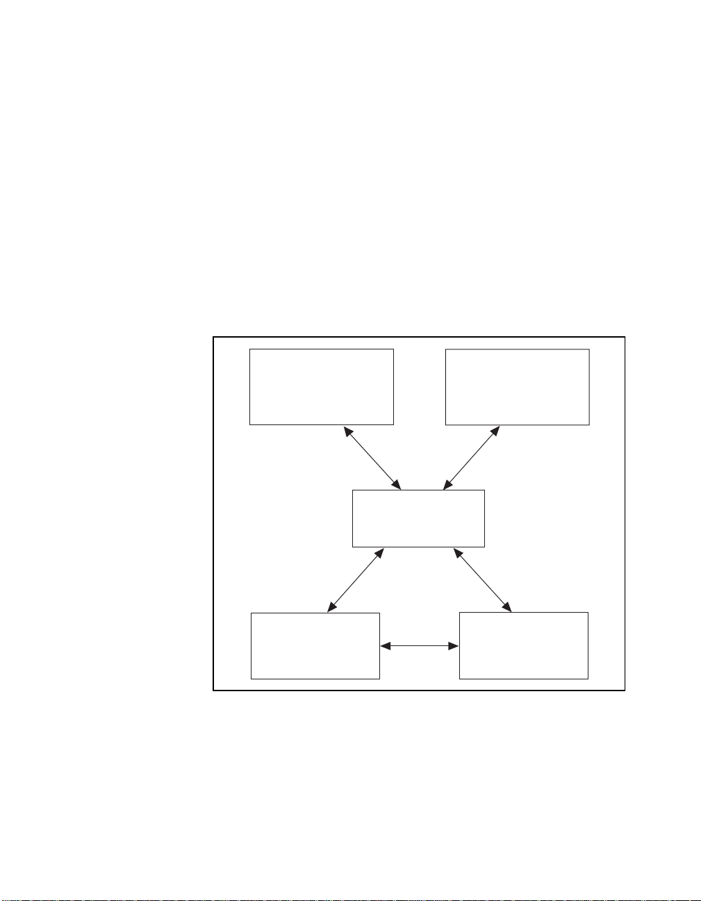
the NI-DAQ driver software, as illustrated in Figure 1-1.
Conventional
Programming Environment
DAQ or
SCXI Hardware
Figure 1-1.
The Relationship between the Programming Environment,
NI-DAQ, and Your Hardware
LabVIEW,
LabWindows/CVI, or
VirtualBench
NI-DAQ
Driver Software
Personal
Computer or
Workstation
DAQArb 5411 User Manual 1-4
©
National Instruments Corporation
Page 14

Optional Equipment
National Instruments offers a var iety of pr odu cts to use w ith yo ur
DAQArb 5411, incl ud ing pro bes , cable s, an d o ther ac cessor i es, a s
follows:
• Shielded and unshielde d I/O con nector b locks (SCB-6 8, TB X-68 ,
CB-68)
•RTSI bus cables
For more specific information about these products, refer to your
National Instruments catalogue or web site, or call the office
nearest you.
Cabling
The following list gives recommended part numbers for cables that you
can use with your 5 411 devic e:
• BNC male to BNC male, 50 Ω cable from ITT Pomona E lectro nics
(part number BNC-C-xx)
• BNC male to BNC male, 75 Ω cable from ITT Pomona E lectro nics
(part number 2249-E-xx)
• BNC female to RC A ph ono plug ada pter, fr om ITT Pom ona
Electronics (part number 5319)
•BNC 50 Ω fe ed -throug h te rminato r adapt er from IT T Pom ona
Electronics (part number 4119-50)
• BNC female -f ema le ad ap te r fr om ITT P om ona El ec tro ni cs
(part number 3283)
Chapter 1 Introduction
©
National Instruments Corporation 1-5 DAQArb 5411 User Manual
Page 15

Chapter 1 Introduction
Unpacking
Your device is shipped in an antistatic package to prevent electrostatic
damage to the device . Ele ctros tatic disc harg e can da mage seve ral
components on the device. To avoid such damage in handling the
device, take the following prec autions:
• Ground yourself via a ground ing strap or by holdin g a grounded
object.
• Touch the anti-static package to a metal part of your computer
chassis before rem oving the d evic e f rom the pack age .
• Remove the device from the package and inspect the device for
loose components or any other sign of d amag e. Notify Na tiona l
Instruments if the device appear s damaged in any way. Do not
install a damaged dev ice into yo ur comp uter .
• Never touch the exposed pins of connectors.
DAQArb 5411 User Manual 1-6
©
National Instruments Corporation
Page 16
Installation and
Chapter
Configuration
This chapter descr ibes how to in stall and conf igure your DAQArb 5411.
Installation
Note:
You should install your driver software before installing your hardware.
Refer to the
installation information.
If you have an older version of NI-DAQ already in your system, that
software will not work with your device. Install NI-DAQ from the NI-DAQ
software CD shipped with yo ur DAQArb 54 11.
You can install the PCI-5411 in any PCI slot and the AT-5411 in any ISA
slot in your comput er. Ho we ver, f or be st n oise perf or manc e, leav e as
much room as p ossi ble b etwee n th e DAQAr b 5 411 and oth er har dwar e.
Before installing your 5411 device, consu lt your PC user man ual or
technical reference manual for specific instructions and warnings.
Follow these general instructions to install your DAQArb 5411:
1. Write down the DAQArb 5411 serial number on the DAQArb 5411
2. Turn off your computer.
3. Remove the top cover or access port to the I/O channel.
4. Remove the expansion slot cover on the back pan el of the
5. For the PCI-5411, insert the card into a PCI slot. For the AT-5411,
6. Screw the mounting bracket of the DAQArb 5411 to the back panel
7. Visually verify the installation.
2
DAQArb 5411 R ea d Me Fir st
Hardware and Software C onfigur ation For m in Appe ndix C,
Customer Communication. You may need this seri al number fo r
future reference if you need to contact technical support.
computer.
insert the card into a 16-bit ISA slot. It may be a tight fit, but do not
force the device into place.
rail of the computer.
document for software
©
National Instruments Corporation 2-1 DAQArb 5411 User Manual
Page 17

Chapter 2 Installation and Configuration
8. Replace the cover.
9. Plug in and turn o n y our com puter.
The PCI-5411 or AT-5 411 is now in stalled .
Hardware Configuration
The DAQArb 5411 is a fully software-con figur able, Plug a nd Play
device. Configuration information is stored in nonvolatile memory. The
Plug and Play services que ry the d evi ce, rea d the in forma tion, a nd
allocate resources for items such as base address, interrupt level, and
DMA channel. After assigning these resources, the operating system
enables the de vice fo r ope ratio n.
Installing the Optional Memory Module
The standard onboard memory for the DAQArb 5411 is 4 MB. You can
upgrade to a 16 MB memory mod ule to store large wa veform buffer s
directly on the card. Perform the following steps to install the new
memory module:
1. Turn off the co mpu ter and remo ve the top c over or ac cess port to
the I/O channel.
2. Unscrew the bracket and remove the DAQArb 5411 from the slot it
has been plugged into.
3. Gently place your DAQArb 5411 on a flat surface with the
component and memory module side facing up.
4. Unfasten the two scre ws on the sid e of the m emor y modu le.
5. Gently unplug the memory modu le from the ma in board and store
the old memory module in an antistatic bag to avoid damage to the
components.
6. Properly align the new 16 MB memory module over the connectors
and plug it into the connectors.
7. Fasten the two sc rew s y ou re mo ved in ste p 4.
8. Follow the regular installation steps described in the Installation
section earlier in this chapter.
DAQArb 5411 User Manual 2-2
©
National Instruments Corporation
Page 18
Chapter
ARB
SYNC
PLL Ref
Dig Out
Signal Connections
This chapter describes the I/O connectors, signal connections, and
digital interface to the DAQArb 5411.
I/O Connector
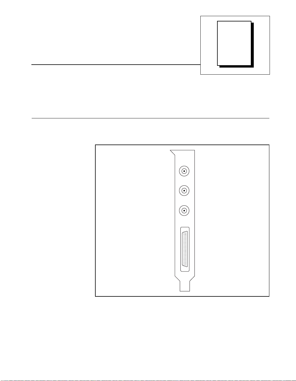
The DAQArb 5411 ha s four con ne ctors: thr ee SM B conne c tors and a
50-pin mini-SCSI type connector , as shown in Figure 3-1 .
3
Figure 3-1.
©
National Instruments Corporation 3-1 DAQArb 5411 User Manual
DAQArb 5411 I/O Connector
Page 19
Chapter 3 Signal Connections
ARB Connector
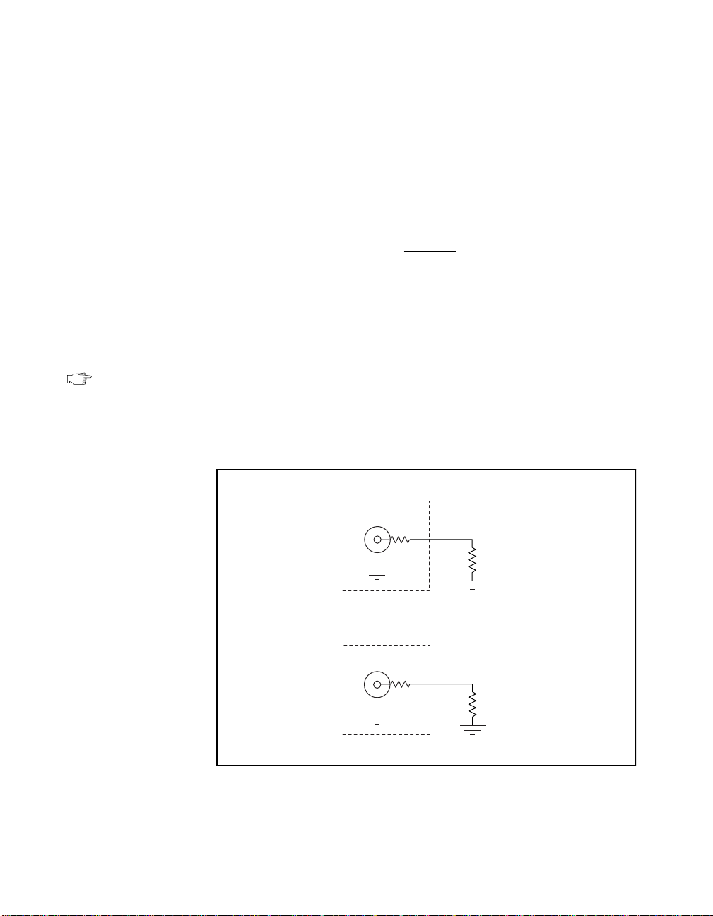
The ARB connector p rov ides the w ave for m outp ut. The ma ximu m
output levels on this connector depend on the type of load termination.
If the output of a DAQArb 5411 terminates into a 50 Ω load, the output
levels are ±5 V, as shown in Figure 3-2. If the output of DAQArb 5411
terminates into a high impedance load (HiZ), the output levels are
±10 V. If the output terminates into any other load, the levels are:
R
V
= ± x 10 V
out
L
RL + R
O
where V
impedance in ohms, and R
DAQArb 5411. By default, R
is the maximum output voltage level, RL is the load
out
is the output impedanc e on the
O
= 50 Ω, but the software can also set it
O
to 75 Ω.
Note: Software will set the voltage output levels based on a 50 Ω load termination.
For more information o n w ave fo rm ge nera tion an d ana log ou tput
operation, refer to Cha pte r 4 , Arb Operation. For specifications on the
waveform output signal, see Appendix A, Specifications.
DAQArb 5411
=
R
50
R
HiZ
Load
=
L
Ω
Load
=
L
±5 V
±10 V
ARB
RO =
Ω
50
50 Ω Load
DAQArb 5411
ARB
R
O
Ω
50
Figure 3-2.
DAQArb 5411 User Manual 3-2
Output Levels and Load Termination Using a 50 Ω Output Impedance
High Impedance Load
©
National Instruments Corporation
Page 20
SYNC Connector
Chapter 3 Signal Connections
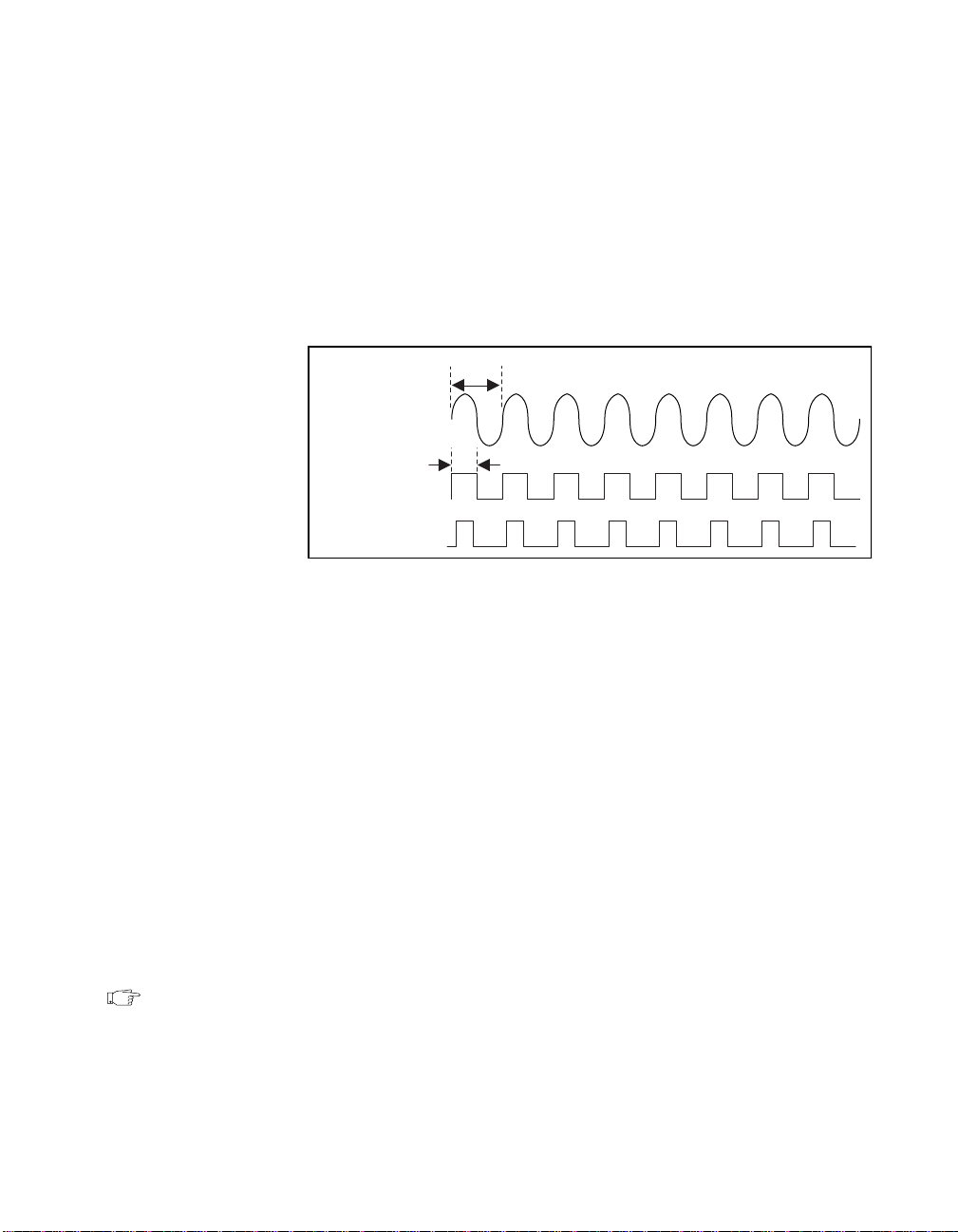
The SYNC c onn ec tor i s a tr an sis to r-t r ans is to r- lo gic (T TL ) versi on o f
the sine waveform being generated at the output. You can think of the
SYNC output as a very high f reque ncy re solution,
software-programmable cloc k source for m an y app lica tions. You ca n
also vary the duty cycle of SYNC output on the fly by software control,
as shown in Figure 3-3. t
generated and t
w/tp)
x 100 %.
is (t
ARB Output
SYNC Output
(50% Duty Cycle)
SYNC Output
(33% Duty Cycle)
is the pulse width of the SYNC output. The duty cycle
w
is the time period of the sine wave being
p
t
p
t
w
PLL Ref Connector
Note: You can also lock the DAQArb 5411 to o ther National Instruments cards
over the RTSI bus using the 20 MHz RTSI clock signal.
Figure 3-3.
SYNC Output and Duty Cycle
You can route the SYNC output to the RTSI lines over the RTSI bus.
The SYNC output is derived from a comparator connected to the analog
waveform and is intend ed to be use d w hen th e wave form is a sine
function. The SYNC output will provide a meaningful waveform only
when you are ge nera ting a sine w ave on the ARB ou tput. For m ore
information on SYNC output, see Chapter 4, Arb Operation.
The PLL Ref connector is a phase-locked loop (PLL) input connector
that can accept a referen ce clock from an e xternal so urce and p hase lock
the DAQArb internal clock to this external clock. Th e refere nce clock
should not deviate more than ±100 ppm of its no minal frequenc y. The
minimum amplitude levels of 1 V
are required on this clock. You can
pp
lock reference clock frequen cies of 1 MHz and 5–2 0 MHz in 1 MHz
steps.
©
National Instruments Corporation 3-3 DAQArb 5411 User Manual
Page 21

Chapter 3 Signal Connections
Dig Out Connector
If no external reference clock is available, the DAQArb 5411 will
automatically tune the internal clock to the best accuracy possible. For
more information on PLL operation, refer to Chapter 4, Arb Operation.
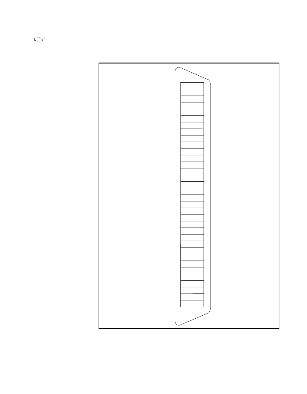
Dig Out is a 16-bit digital I/O connector that contains the 16-bit digital
pattern outputs, digital pattern clock outp ut, marke r ou tput, exter nal
trigger input, and power output.
Connector Pin Assignments
Figure 3-4 shows the DAQArb 5411 50-pin digital connector.
DAQArb 5411 User Manual 3-4
©
National Instruments Corporation
Page 22

Chapter 3 Signal Connections
DGND
NC
DGND
NC
DGND
NC
DGND
+5V
DGND
MARKER
DGND
RFU
DGND
RFU
DGND
PA(13)
DGND
PA(13)
DGND
PA(7)
DGND
PA(4)
DGND
PA(1)
DGND
50
EXT_TRIG25
2449
2348
2247
2146
2045
1944
1843
1742
1641
1540
1439
1338
1237
1136
1035
NC
NC
NC
NC
NC
NC
+5V
+5V
+5V
PCLK
RFU
RFU
RFU
PA(15)
PA(14)
934
PA(12)
833
PA(11)
732
PA(9)
631
PA(8)
530
PA(6)
429
PA(5)
328
PA(3)
227
PA(2)
126
PA(0)
Figure 3-4. DAQArb 5411 50-Pin Digital Output Connector Pin Assignments
Signal Descriptions
Table 3-1 gives the pin name s and signa l descrip tions u sed o n the
DAQArb 5411 digital output connector.
©
National Instruments Corporation 3-5 DAQArb 5411 User Manual
Page 23

Chapter 3 Signal Connections
Table 3-1.
Digital Output Connector Signal Descriptions
Signal Name Type Description
DGND – Digital ground
EXT_TRIG Input External trigger—The external trigger input signal is a
TTL-level signal that you c an use to sta rt or step thr ough a
waveform generation. For more information on trigger sources
and trigger mode, see Chapter 4, Arb Operation .
MARKER Output Marke r—A marker is a TTL-level output signal that you can set
up at any point in the waveform being gene rated. You can use
this signal to synchronize or trigge r o ther d ev ices a t a c erta in
time within waveform generation.
NC – Not connected.
PA<0..15> Output Digital pattern generator—The 16-bit dig it al re pr ese nta tio n of
the analog waveform is available as digital pattern outputs
along with the clock to which it is synchronized. This data is
available directly from the memory after some sample clocks
pipeline delay. The digital pattern outputs are available as TTL
output levels.
PCLK Output Digital pattern clock —The digital pattern clock output
synchronizes the digital pattern output. This data is available
directly from the memory after some sample clocks pipeline
delay. The clock output is available as a TTL output level.
RFU – Reserved for future use. Do not connect signals to this pin.
+5V Output +5 V p ow er —A +5 V ou tput signal is availa ble on the DAQArb
to power external devices. The maximum current you can draw
is 100 mA.
SHC50-68 50-Pin Cable Connector
You can use an optional SHC50-68 50-pin to 68-p in cable for pattern
generator output. The cable connects to the digital outpu t connector on
the DAQArb 5411. Figure 3-5 shows the 68-pin connector pin
assignments on the SHC50-68 ca ble.
©
DAQArb 5411 User Manual 3-6
National Instruments Corporation
Page 24
Chapter 3 Signal Connections
Note: The SHC50-68 connector use s the sa me signals as the D AQArb 5411
digital output connector, shown in Table 3- 1.
PA(0)
PA(1)
PA(2)
PA(3)
PA(4)
PA(5)
PA(6)
PA(7)
PA(8)
PA(9)
PA(10)
PA(11)
PA(12)
PA(13)
PA(14)
PA(15)
MARKER
RFU
PCLK
RFU
RFU
RFU
RFU
+5V
NC
NC
NC
NC
NC
NC
NC
NC
NC
EXT_TRIG
23
26
27
28
29
30
31
32
33
34
10
11
12
13
14
15
16
17
18
19
20
21
22
24
25
1
35
2
36
3
37
4
38
5
39
6
40
7
41
8
42
9
43
44
45
46
47
48
49
50
51
52
53
54
55
56
57
58
59
60
61
62
63
64
65
66
67
68
DGND
DGND
DGND
DGND
DGND
DGND
DGND
DGND
DGND
DGND
DGND
DGND
DGND
DGND
DGND
DGND
DGND
DGND
DGND
DGND
DGND
DGND
DGND
+5V
DGND
DGND
DGND
DGND
DGND
DGND
DGND
DGND
DGND
DGND
Figure 3-5. SHC50-68 68-Pin Connector Pin Assignments
©
National Instruments Corporation 3-7 DAQArb 5411 User Manual
Page 25

Chapter 3 Signal Connections
Power-Up and Reset Conditions
When you power-up your computer, the DAQArb 5411 is in the
following state:
• Output is disabled and set to 0 V
• Sample clock is set to 4 0 MH z
• Trigger mode is set to continuous
• Trigger source is set to automatic (the software provide s the
triggers)
• Digital f ilt e r is enabled
• Output attenuation remains unchanged from previous setting
• Analog filter remains unchanged from previous setting
• Output impedance remains unchanged from previous setting
• Digital pattern generatio n is disa bled
When you reset the board usin g NI -DA Q or any ap plication sof tware
calling NI-DAQ, your DAQArb is in the following state:
• Output is disabled and set to 0 V
• Sample clock is set to 4 0 MH z
• Trigger mode is set to continuous
• Trigger source is set to automatic (the software provide s the
triggers)
• Digital f ilt e r is enabled
• Output attenuation is set to 0 dB
• Analog filter is enabled
• Output impedance is set to 50 Ω
• Digital pattern generatio n is disa bled
• PLL reference frequ en cy i s se t t o 20 MH z
• PLL reference source is se t to in ternal tuning
• RTSI clock source is disabled
• SYNC duty cycle is set to 50%
DAQArb 5411 User Manual 3-8
©
National Instruments Corporation
Page 26
Chapter
Arb Operation
This chapter describes how to use your DAQArb 5411.
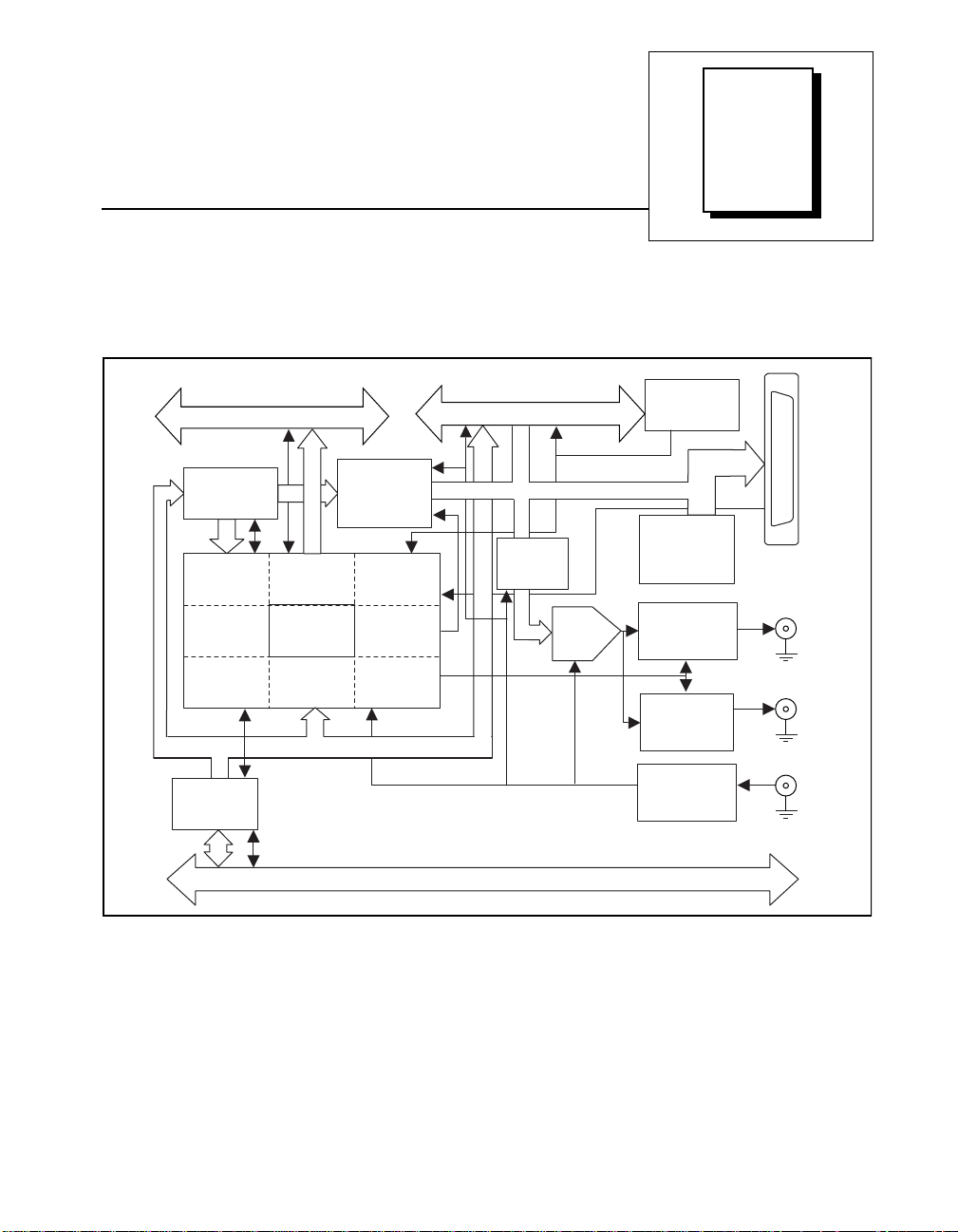
Figure 4-1 shows the DAQArb 5411 block diagram.
RTSI Bus
Instruction
FIFOs
IFIFO
Control
Clock
Controls
Filter
Controls
Bus
Interface
RTSI
Control
Waveform
Sequencer
Trigger
Control
Data Path
DDS +
Lookup
Memory
AMM
Control
DDS
Control
Analog
Control
Memory Connector
Digital
Filter
DAC
Memory
Controller
Pattern
Generation
Circuit
Attenuators,
Filter, and
Amplifier
Level
Crossing
Detector
PLL and
Clocking
4
Digital Connector
ARB
SYNC
PLL Ref
ISA/PCI Channel
Figure 4-1.
DAQArb 5411 Block Diagram
The DAQArb 5411 consists of a bus interface that communicates with
the ISA bus for the AT-5411 or the PCI bus for the PCI -54 11. The bus
interface block handles Plug and Play protocols for assigning resources
to the device and providing drivers for the data and address bus that are
local to the device. The waveform sequencer performs multiple
©
National Instruments Corporation 4-1 DAQArb 5411 User Manual
Page 27

Chapter 4 Arb Operation
functions such as arbitrating the data buses and controlling the triggers,
filters, attenuators, clocks, PLL, RTSI switch, instruction FIFO, and
direct digital synthesizer (DDS). The memory controller controls the
waveform memory on the memory module. The data from the memory
is fed to a digital to analog converter (DAC) through a half-band
interpolating digital filter. The output from the DAC goes through the
filter, amplifiers, attenuators and, finally, to the I/O connector.
Waveform Generation
The DAQArb 5411 can generate w aveform s in two modes: Arb an d
DDS. Use Arb mode for any arbitrary waveform generation, but you can
use DDS mode for standa rd f reque nc y ge nera tio n such a s sin e, T TL,
square, and triangular waveforms.
In Arb mode, you can define waveforms as multiple buffers. You can
link and l oop these buffers in any order you desire. This mode has more
features and is more flexible than DDS mode.
Note: If you use Virtual Bench software, you must use VirtualBench-Arb for Arb
mode.
DDS mode is more suitable for generating standard waveforms that are
repetitive in nature, for example, sine, TTL, square, and triangular
waveforms. In DDS mode, you are limited to one buffer, and the buffer
size must be exactly equal to 16,384 samples.
Note: If you use VirtualBench software, you must use VirtualBench-Function
Generator for DDS mode.
Figure 4-2 shows a block diagram representation of the data path for
waveform generation. The data for waveform generation can come from
either the waveform memory module or DDS lookup memory,
depending on the mod e of w avefor m g ener ation. Th is da ta is
interpolated by a half-band digital filter and then fed to a high-speed
DAC. The data has a pipeline delay of 26 update clocks through this
digital filter.
DAQArb 5411 User Manual 4-2
©
National Instruments Corporation
Page 28

ARB Memory
12 Bits
16 Bits
Mode Select
DDS Lookup
Memory
DDS
Digital Filter
Digital Filter
Enable
Chapter 4 Arb Operation
A
Filter
12
MUX
B
DAC Register
DAC12
Update Rate
Note: For DDS mode, you should always keep the update rate at 40 MHz.
Arb Mode
16-Bit
Counter
Figure 4-2. Waveform Data Path Block Diagram
Div/2
80 MHz Oscillator
On the DAQArb 5411, the high-speed DAC itself is always updated at
80 M Hz b ut th e ma ximu m update cl ock f or wav efor m me mor y is
40 M Hz. The up date cloc k for the wavefo rm mem ory can be further
divided by a 16-bit cou nter, a s sho wn in Figur e 4- 2. T here fore, the
slowest update rate is 40 MH z d ivide d b y 65, 536 , which is 6 10. 35 H z.
Doing this will yield the best performance of the combination of DDS,
digital filter, DAC, and analog filter.
The Arb mode of wavefor m genera tion uses a separate waveform
memory for storing multiple waveform buffers. This mode also uses a
FIFO memory for storing the staging list, which contains the buffer
linking and looping information. This FIFO is referred to as an
instruction FIFO.
©
National Instruments Corporation 4-3 DAQArb 5411 User Manual
Page 29

Chapter 4 Arb Operation
Waveform Size and Resolution
The DAQArb 5411 store s arbitra ry w avef orm s in m em ory a s 1 6-b it
digital words. Only the 12 most significant bits are sent to the digital
filter and the DAC. The following sections describe the waveform
memory, the sizes available, and minimum buffer size.
Waveform Memory
The DAQArb 5411 uses a waveform memory16 bits wide. The standard
memory size is 2,000,000 samples. This large memory means you can
store very long waveforms on the board itself and obtain reliable
waveform generation even at full speed. You can upgrade to an
8 million-sa mple wavef orm memory by installing the op tional 16 MB
memory module. See Cha pter 2, Installation and Configu ration, for
more information on the memory module.
As shown in Figure 4-3, a 2,000,000-sam ple wavef orm memor y is
organized as eight banks of 256 k by 16-bit memory chips. These eight
banks are then shifted serially to achieve a single data stream of 16-bit
words at 40 MHz.
2 M Words
(8 M Words)
256 k X 16 bits
(1 M X 16 bits)
256 k X 16 bits
(1 M X 16 bits)
256 k X 16 bits
(1 M X 16 bits)
256 k X 16 bits
(1 M X 16 bits)
256 k X 16 bits
(1 M X 16 bits)
256 k X 16 bits
(1 M X 16 bits)
256 k X 16 bits
(1 M X 16 bits)
256 k X 16 bits
(1 M X 16 bits)
16
16
16
16
16
16
16
16
16
Waveform Data
Pipeline + Load + Shift Register
Memory
Control Lines
Figure 4-3.
DAQArb 5411 User Manual 4-4
Clock
Waveform Memory Architecture
©
National Instruments Corporation
Page 30

Minimum Buffer Size and Resolution
The 5411 device m emor y archite cture imp oses ce rtain re strict ions on
the buffer size and resol ution. The minimum buffer size for Ar b mode
is 256 samples and the buffers must be in multiples of eight samples.
For example, if you request the DAQArb to load a buffer of 257
samples, NI-DAQ will truncate the buffer to 256 samples. The last
sample will not be loaded into the memory.
Note: If the minimum buffer size of 256 samples is not met, NI-DAQ will return
an error.
Note: If the buffer is not a multiple of eight samples, NI-DAQ will return a
warning and truncate the buffer to the nearest multiple of eight samples.
Waveform Linking and Looping
Before you can start generating waveforms, you have to load the buffers
on your DAQArb 5411. Each signal to be generated loads into the
memory in the form of 16-bit digital samples. A finite number of these
samples makes a waveform buffer, sometimes also referred to as a
waveform segment. You can load multiple buffers in the memory on
DAQArb 5411. To generate these buffers, you have to prepare a staging
list, also known as a sequence list, which contains a sequence of stages.
Each stage specifies the buffer to be generated, the number of loops on
that buffer, and the marker position for that buf fer.
Chapter 4 Arb Operation
Figure 4-4 illustrates the concept of waveform samples, buffer, stage,
staging list, and looping and linkin g. Wa vefor m sample A shows the
concept of wave form s ample s used t o crea te a wav eform , sho wn in
waveform buffer 1. In this example, the waveform buffer 1 represents a
single cycle of a sine wave and the waveform samples in sample A are
16-bit samples. Waveform stage 1 shows a stage created from buffer 1.
Stage 1 is buffer 1 with three cycle iterations.
Waveform sample B shows samples for waveform buffer 2, which
represents a triangular wavefo rm. Wa veform stage 2 is created using
two iterations of buffer 2.
Stage 3 is created using a single iteration of buffer 1. These waveforms
are linked in a sequence, as shown in Figure 4-4. The co ncep t of us ing
a staging list to ge ne rat e wa vefo rms is re ferre d to as waveform linking
and looping or waveform staging.
©
National Instruments Corporation 4-5 DAQArb 5411 User Manual
Page 31

Chapter 4 Arb Operation
Waveform
Sample A
Waveform
Sample B
Waveform
Buffer/Segment 1
Waveform
Buffer/Segment 2
Stage 1
Waveform Linking (Staging List)
Waveform Stage 2
Stage 2 Stage 3
Waveform Stage 1
(Loops = 3)
(Loops = 2)
Figure 4-4. Waveform Linking and Looping
Waveform Staging
Figure 4-5 shows waveform staging in hardware. The instruction FIFO
contains the staging list, which the DAQArb 5411 sequencer reads for
waveform generation.
DAQArb 5411 User Manual 4-6
©
National Instruments Corporation
Page 32

Chapter 4 Arb Operation
Data In (16) Data Out (16)
Instructions
Address Generator
Buffer Number
Buffer Size
Buffer Loops
Marker Offset
Instruction FIFO
Waveform Memory
Address
Sequencer
+
16-Bit
Counter
Memory
Controller
Div/2
Figure 4-5. Waveform Staging Block Diagram
Each stage is made up of four instructions:
• Buffer number—Specifies the buffer number to be generated .
• Buffer size—Specifies the total count of the buffer to be generated.
This count may be more or less than the actua l size of that buffer.
If the count is less, only a part of that buffer will be used for that
stage. If the count is more than the actual size of that buffer, part of
the next sequential buffer will also be used. If the buffer size is set
to zero, the software will automatically use the true size of that
buffer.
• Buffer loops —Specifies the number of times that buffer has to be
looped. The maximum n umb er of loops pos sib le is 65,53 5.
• Marker offset—Specifies where the marker has to be generated
within that buffer. For more information on markers, see the
Markers section later in this chapter.
80 MHz Oscillator
Note: The maximum number of wa vef o rm stages the instruction FIF O c an sto re
for Arb mode is 290.
Note: For more information on the waveform generation pr ocess, refer to your
software manuals.
Figure 4-6 shows a sim ple c ase o f wave fo rm ge nera tion proc ess.
©
National Instruments Corporation 4-7 DAQArb 5411 User Manual
Page 33

Chapter 4 Arb Operation
y
Reset Device
Setup Clocks and Triggers
Load Buffers Sequentially
Load Staging List
Start Waveform Generation
Stop
Yes
STOP Waveform Generation
Figure 4-6. Waveform Generation Process
Direct Digital Synthesis (DDS) Mode
Direct digital synthesis (DDS) is a technique for deriving, under digital
control, an analog frequency sour ce from a single reference clock
frequency. This technique provides high-frequency accuracy and
resolution, temperature stability, wideband tuning, and very fast and
phase-continuous frequency switching.
No
Filter, Attenuation,
Impedance, Output
Enable Setups
On the Fl
DAQArb 5411 User Manual 4-8
©
National Instruments Corporation
Page 34

Chapter 4 Arb Operation
The DAQArb 5411 uses a 32-b it, high-speed acc umulator with a loo kup
memory and a 12-bit DAC for DD S-base d wavefo rm genera tion.
Figure 4-7 sh ows the building bloc ks for DDS- ba sed w avefor m
generation.
Frequency
Time
Frequency
Time
Instruction FIFO
DDS
Sequencer
16-Bit
Counter
(14)
Lookup
Memory
Figure 4-7. DDS Building Blocks
Div/2
Data Out (16)
80 MHz Oscillator
The lookup memory is d edicated to th e DD S mo de only a nd ca nn ot be
used in Arb mode. You can store one cycle of a repetitive
waveform—a sine wave, a tr iangular wa ve, a squar e wave, or an
arbitrary wave—in the loo kup m em ory. Th en, you c an c hange the
frequency of that waveform by sending just one instruction. You can
use DDS mode for very fine freq ue ncy r esolution f un ction ge ne ration.
You can generate sine waves of up to 16 MHz with a frequenc y
resolution of 10.0 mHz. Because this mode uses an accumulator,
waveform generation loops back to the beginning of the lookup memory
after passing through th e en d of the look up memo ry.
You should use DDS mode for standard function generation rather than
for arbitrary wa ve fo rm ge ne ration.
In this mode, each stage is made up of two instructions: the frequency,
which specifies the f reque ncy of the wa vefor m to b e gene rated , a nd
time, which specifies the time for which the frequency has to be
generated.
©
National Instruments Corporation 4-9 DAQArb 5411 User Manual
Page 35

Chapter 4 Arb Operation
Frequency Resolution and Lookup Memory
For DDS-based wavefor m gene ration, you m ust firs t load on e cyc le o f
the desired waveform into the lookup memory. The size of the DDS
lookup memory is 16,384 sample s. Each samp le is 16 bits wide.
Note: One cycle of the waveform buffer loaded into the memory should be exactly
equal to the size of the DDS lookup memory.
= update clock for the accumulator
F
c
Set the DAQArb 5411 at F
F
= desired frequenc y o f th e output sign al
a
= 40 MHz.
c
N = accumulator size in bits
Set the DAQArb 5411 at N = 32.
FCW = frequency control word to be loaded into the accumulator
to generate F
.
a
This is calculated using the formula:
FCW = (2
N
* Fa) / F
c
The frequency resolution is then given by:
frequency resolution = F
/ 2N = (40 x 106) / 232 = 9.31322 mHz
c
For example, if you need to genera te a freque ncy of 10 MHz , then the
32
FCW is (2
generate a frequency of 1 Hz, then the FCW is (2
* 10E6)/40E6, which equals 1,073,741,824. If you need to
32
* 1)/40E6, which
equals 107.
Note: On the DAQAr b 541 1, t he ma ximu m f req uenc y of a sin e w a ve y ou ca n
generate reliably is limited to 16 MHz. Other waveforms like square or
triangular waves are limited to 1 MHz.
You can also synt hesize arb itrar y wa vefo rms using DD S. Gen erating
arbitrary waveforms this way will be very limited; you are restricted to
a single buffer, and this buffer should be exactly equal to the size of the
lookup memory.
To update ever y nex t sa mple o f an arbitrar y w ave form in lo oku p
memory at the maximum clock rate of 40 MHz, write an FCW value of
(N-L)
, where N is the size of the accumulator and L is the number of
2
address bits of lookup m em ory ( L = 14 bits for the A T-54 11 and th e
PCI-5411). Thus, the FCW value for the DAQArb 5411 equals 262,144.
DAQArb 5411 User Manual 4-10
©
National Instruments Corporation
Page 36

If you want to up da te ev er y n ext samp le in loo kup me mo ry a t a n
integral subdivision, D, of the maximum clock rate, you should write an
FCW value of 2
every sample at half the maximum clock rate, you should write an FCW
value of 2
(N-L-D+1)
(32-14-2+ 1 )
Frequency Hopping and Sweeping
You can define a s taging list in DD S mo de f or perf orm ing freq uency
hops and sweeps. The en tir e st ag in g li st u se s t he sa m e buffe r lo ad ed
into the lookup memory. A ll stage s diffe r in the fre qu ency to be
generated. As shown in Figure 4-7, a stage in DDS mode has a different
instruction set than Arb mode.
Note: The minimum time that a f requenc y should be generate d is at leas t 2 µs.
Therefore, the maximum hop rate from one frequency to the other
frequency is limited to 500 kHz.
Note: The maximum number of stages that can be stored in the instruction FIFO
for DDS mode is equal to 340. For more information on the waveform
generation process, refer to your software manuals.
Chapter 4 Arb Operation
. In other words, fo r an effe ctive updat e rate of
, which equals 131,072.
Triggering
Triggering is a featur e by whic h you c an sta rt and step thr oug h a
waveform generation. T he tr igge r source s an d trig ger mod es ar e
explained in th e sect ion s below .
Trigger Sources
Trigger sour ces ar e s of twa re se le ct ab le. B y d ef au lt, t h e soft wa re
provides the triggers. You can use also use an external trigger from a
pin on the digital I/O connector or from any of the RTSI trigger lines on
the RTSI bus. Figure 4-8 shows the trigger sources for the
DAQArb 5411.
©
National Instruments Corporation 4-11 DAQArb 5411 User Manual
Page 37

Chapter 4 Arb Operation
RTSI Trigger
Lines <0..6>
7
RTSI Switch
RTSI Trigger
External Trigger
Software Trigger
Trigger Select
Modes of Operation
Digital
MUX
Figure 4-8. Waveform Generation Trigger Sources
Start Trigger
If you need to automatically trigger the waveform generation, use
software to generate the triggers. A rising TTL edge is required for
external triggering. For more information on triggering over RTSI lines,
see the RTSI Trigger Lines section later in this chapter.
DAQArb 5411 functionality is further enhanced by various triggering
modes available on it. The available trigger modes are single,
continuous, stepped, a nd burst. Th ese trig ger mod es a re a vailable for
both arb and DDS modes.
Single Trigger Mode
The waveform you describe in the sequence list is generated only once
by going through the entire staging list. Only one trigger is required to
start the waveform generation.
You can use single trigger mode with the both the Arb and DD S
waveform generation modes, as fo llows:
• Arb mode—Figure 4 -9 uses th e stag es 1, 2, and 3 sho wn in
Figure 4-4 to illustrate a single trigger mode of opera tion for Arb
waveform generation mode. After the DAQArb 5411 receives a
trigger, the wavefo rm ge nera tion starts f rom the first stage and
continues through to the last stage. The last stage is generated
repeatedly until you stop the waveform generation.
DAQArb 5411 User Manual 4-12
©
National Instruments Corporation
Page 38

Start Trigger
Chapter 4 Arb Operation
End of All Stages
Last Stage Generated Continuously Until Stopped
Figure 4-9. Single Trigger Mode for Arb Mode
Note: You can settle to a predefined state by making the last stage emulate that
state.
• DDS mode—After the DAQArb 5411 receives a trigger, the
waveform generation starts f rom the first stage and c ontin ues
through to the last stage. The last stage is generated repeatedly until
the waveform generation is stopped. Figure 4-10 illustrates a single
trigger mode of ope ration f or DD S wa ve form gener a tion m ode .
Start Trigger
f1, ∆T1
End of All Stages
f2, ∆T2
f3, ∆T3
Figure 4-10. Single Trigger Mode for DDS Mode
Last Stage Generated
f4
Continuously Until Stopped
Assume that one cycle of a sine wa ve is sto red in th e D DS loo kup
memory. For stage 1, f1 specifies the sine frequency to be
generated for time ∆T1, f2 and ∆T2 for stage 2, and so on. If there
are four stages i n the st agin g list , then f4 will be genera ted
continuously until the waveform generation is stopped.
Continuous Trigger Mode
The waveform you describe in the staging list is generated infinitely by
recycling through all the staging list. After a trigger is received, the
waveform generation starts f rom the first stage and c ontin ues throug h
to the last stage. After the last stage is completed, the waveform
generation loops back to the start of the first stage and continues until
it is stopped. Only one trigger is required to start the waveform
generation.
©
National Instruments Corporation 4-13 DAQArb 5411 User Manual
Page 39

Chapter 4 Arb Operation
Start Trigger
You can use con tinuous trigger m ode w ith th e both the A rb a nd DD S
waveform generation modes, as fo llows:
• Arb mode—Figure 4-11 u ses the sta ges sho wn in Figur e 4- 4 to
illustrate a continuous trigger mode of operation for Arb waveform
generation mode.
Repeat
Until Stopped
End of All Stages
Figure 4-11. Continuous Trigger Mode for Arb Mode
End of All Stages
• DDS mode—Figure 4-12 illustrates a continuous trigger mode of
operation for DDS waveform gene ration mode.
Start Trigger
(f1, ∆T1)
End of All Stages
(f2, ∆T2)
(f3, ∆T3)
(f4, ∆T4)
Figure 4-12. Continuous Trigger Mode for DDS Mode
(f1, ∆T1)
Repeat
Until Stopped
(f2, ∆T2)
Stepped Trigger Mode
After a start trigger is received, the waveform described by the first
stage is generated. Then, the device waits for the next trigger signal. On
the next trigger, the waveform desc ribed by the second stag e is
generated, and so on. Onc e the staging list is exh austed, the w aveform
generation returns to the first stage and continues in a cyclic fashion.
You can use the stepped trigger mode with the both the Ar b and DDS
waveform generation modes, as fo llows:
• Arb mode—Figure 4-13 u ses the sta ges sho wn in Figur e 4- 4 to
illustrate a stepped trigger mod e of ope ration for the Arb m ode. If
a trigger is received while a stage is being generated, it will be
ignored. A trigger will be recognized only after the stage has been
completely generated.
DAQArb 5411 User Manual 4-14
©
National Instruments Corporation
Page 40

Chapter 4 Arb Operation
Start Trigger
End
of Stage 1
*The first eight samples of the next stage are generated repeatedly.
Start Trigger
*
End
of Stage 2
Start Trigger
End
of Stage 3
Figure 4-13. Stepped Trigger Mode for Arb Mode
Start Trigger
Repeat Sequence
Keep Going
Until Stopped
End
of Stage 1
After any stage has been generated completely, the first eight
samples of the next stage are repeated continuously until the next
trigger is received.
Note: For stepped trigger mode, you can predefine t he state in which a stage ends
by making the first eight samp les of the nex t stag e rep resen t the state y ou
want to settle.
• DDS mode—Step p e d tr igger mod e and burst trigger mode are t he
same thing for the D DS mode o f wa vefo rm gene ration.
Burst Trigger Mode
After a start trigger is received, the waveform described by the first
stage is generated until another trigger is received. At the next trigger,
the buffer of the p re viou s sta ge i s c om pl ete d befo re th e w ave fo rm
described by the second stage is gene rated. On ce the stag ing list is
exhausted, the waveform generation returns to the first stage and
continues in a cyclic fa shion.
You can use burst tr igger mo de with the both the Arb and D DS
waveform generation modes, as fo llows:
• Arb mode—Figure 4-14 u ses the sta ges sho wn in Figur e 4- 4 to
illustrate a burst trigger mode o f ope ration for Arb mode .
©
National Instruments Corporation 4-15 DAQArb 5411 User Manual
Page 41

Chapter 4 Arb Operation
Start Trigger
Start Trigger
Start Trigger
End
of Stage 1
Start Trigger
End
of Stage 2
End
of Stage 3
Start Triggers
End
of Stage 1
Continues In This
Way of Triggering
Until Stopped
Figure 4-14. Burst Trigger Mode for Arb Mode
• DDS mode—Figure 4-15 illustrates a burst trigger mode of
operation for DDS mode. The switching from one stage to the other
stage is phase continuous. In this mode the time instruction is not
used. The trigger paces the waveform ge neration fro m one
frequency to the other.
Start Trigger
f1 f2
Start Trigger
f3
End of All Stages
Start Trigger
f4
Start Trigger
f1
Figure 4-15. Burst Trigger Mode for DDS Mode
Marker Output Signal
A marker is equivalent to a trigger output signal and it is available on a
separate pin in the digital I/O connector. You can define this TTL level
trigger output signal at an y p osition in the wave fo rm bu ff er. Yo u c an
place a marker in every stage; however, only one marker per stage is
allowed.
You can specify a marker by giving an offset coun t (in number of
samples) fro m th e s ta rt o f th e wa ve fo rm bu ff er s pe ci fied b y th e st ag e.
If the offset is out of range of the number of samples in that stage, the
marker will not appear at the output. If the buffer is looped multiple
times in a stage, the marker will be generate d that many times.
DAQArb 5411 User Manual 4-16
©
National Instruments Corporation
Page 42

Chapter 4 Arb Operation
Note: The marker is generated f or eight upda te cl ocks and the plac eme nt
resolution of the marker is ±4 samples.
If you want a marker at an offset of zero from the start of the waveform
buffer, the marker will be eight samples long beginning with the first
sample. A mark er a t a n off set of seve n from th e star t of the wa ve form
buffer also will be eight samples long beginning with the first sample,
as shown in Table 4-1. A marker at an offset of e ight will be generated
at positions 8– 15.
Table 4-1. Generated Marker Positions
Sample
Number
Marker
Requested
Marker
Generated
1 At sample 0 from the beginning of the buffer Sample position 0–7
2 At sample 1 from the beginning of the buffer Sample position 0–7
3 At sample 7 from the beginning of the buffer Sample position 0–7
4 At sample 8 from the beginning of the buffer Sample position 8–15
5 At sample 255 from the beginning of the buffer Sample position 248–255
Figure 4-16 shows an analog wa veform being genera ted at one
connector and a marker being ge nerated at another I/O conne ctor.
Point A shows a marker generated for requested positions 0–7, and
point B shows requested positions of 8–15.
ARB Output
t
m
A
Marker Output
B
Figure 4-16. Markers as Trigger Outputs
©
National Instruments Corporation 4-17 DAQArb 5411 User Manual
Page 43

Chapter 4 Arb Operation
Note: Marker output signals are an imp ortant fe ature to trigger other
instruments or devices at a specified time while a waveform generation is
in progress.
Analog Output
Figure 4-17 shows the essential blocks of analog waveform generation.
The 12-bit digital wavefor m da ta is fe d to a high-spe ed DA C. A
low-pass filter filters the DAC output. This filtered signal is
pre-amplified before it goes to a 10 dB attenuator. The DAC output can
be fine-tuned for gain and offset. Since the offset is adjusted before the
main attenuators and amplifier, it is referred to as pre-attenuation
offset. This fine-tuning of gain and offset is done using separate DACs.
The output from the 10 dB attenuator is then fed to the main amplifier,
which can provide ±5 V levels into 50 Ω. An output relay can switch
between ground level and the main amplifier. The output of this relay is
fed to a series of passive attenuators. The output of the attenuators is fed
through a selectable outpu t imped ance o f 50 or 75 Ω to the I/O
connector.
10 db
Attenuator
Main Amp
Comparator
+
-
12
Clock
DAC
Low-Pass
Filter
Gain
DAC
Offset
DAC
Level
DAC
Pre Amp
Figure 4-17.
Figure 4-18 shows the timing relationships of the trigger input,
waveform output, and mark er ou tput. T
trigger signal. T
DAQArb 5411 User Manual 4-18
is the time delay from tr igge r to output on Arb
d2
Attenuators
(63 dB in 1 dB steps)
Output
Enable
50 Ω
50 Ω
25 Ω
50 Ω/75 Ω
Selector
Analog Output and SYNC Out Block Diagram
is the pulse width on the
d1
©
National Instruments Corporation
ARB
SYNC
Page 44

output. Td3 is the time between the marker output and Arb output.
is the pulse width on mar ker o utput. Ref er to Appe ndix A,
T
d4
Specifications, for more information on these timing parameters.
Trigger Input Signal
(Slope: Positive, TTL)
Waveform Output
(±5 V
Marker Output
(TTL)
pp
into 50 Ω
)
Note: You can switch off the analog low-pass filter at any time during waveform
generation.
SYNC Output and Duty Cycle
The SYNC output is a TTL ve rsion o f the sine wa vefor m being
generated at the output. The signal from the pr e-am plifier is sent to a
comparator, where it is compared against a level set by the level DAC.
The output of this comparator is sent to the SYNC connector through a
hysteresis buffer and a 50 Ω series resistor to provide reve rse
termination of reflected pulses.
Chapter 4 Arb Operation
T
d1
T
d2
T
d3
T
d4
Figure 4-18. Waveform, Trigger, and Marker Timings
You can use the SYNC output as a very high freque ncy resolution,
software-programmable cloc k source for m an y app lica tions. You also
can vary the duty c yc le of SYN C outpu t, o n the fly, b y c hang in g the
output of the level DAC. The SYNC output might not carry any meaning
for any other types of waveforms being generated.
Note: You can change the duty cycl e of SY NC outp ut at an y time during
waveform generation.
Output Attenuation
Figure 4-19 shows the DAQArb 5411 ou tput attenuato r chain. The
output attenuators are ma de of resistor netw orks and may be switc hed
in any combination desired. The m axim um atte nuation po ssible o n the
DAQArb 5411 is 73 dB.
©
National Instruments Corporation 4-19 DAQArb 5411 User Manual
Page 45

Chapter 4 Arb Operation
1 dB
In
2 dB 4 dB
By attenuating the output sig nal, you ke ep the dyna mic r ange o f the
DAC; that is, you do not lose any bits from the digital representation of
the signal because the attenuation is done after the DAC and not
before it.
attenuation (in decibels) = –20 log
where,
V
= desired voltage level for the output signal
o
V
= input voltage level.
i
Note: For the DAQArb 5411, V
unterminated load.
For example, to change the output level to ±2.5 V into a terminated
load, use the following formula:
Attenuation = –20*log
8 dB
16 dB
32 dB
Figure 4-19. Output Attenuation Chain
(V
/Vi)
10
o
= ±5 V for terminated load and ±10 V for
i
(2.5/5) = 6.020 dB
10
Out
Note: You can change the output attenuation at any time during waveform
generation.
Output Impedance
As shown in Figure 4- 17, bef ore th e signal r eac hes the o utput
connector, you can select the outp ut impedance to be 50 Ω or 7 5 Ω. If
the load impedance is 50 Ω and all the attenuators are off (that is, an
output attenuation of 0 dB ), the o utput levels a re ±5 V.
A load impedance of 50 Ω is used for most applications but 75 Ω is
required for applications such as testing video devices. If the load is a
very high input impedance load (~1 MΩ), you will see output levels up
to ±10 V.
Note: You can change the output im pedance at any time du ring wa vefo rm
generation.
DAQArb 5411 User Manual 4-20
©
National Instruments Corporation
Page 46

Output Enable
You can switch off the waveform generation at the output connector by
controlling the output enable relay, as shown in Figure 4-17. When the
output enable relay is off, the output signal level goes to ground level.
Note: Even though the output enable relay is in the off position, the waveform
generation process will continue internally on the DAQArb 5411.
You can use this feature to disconnect and connect different devices, on
the fly, to the DAQArb 5411.
Note: You can change the output en able state at a ny time during wa vefo rm
generation.
Pre-attenuation Offset
Pre-attenuation offset is an offset adjustment to the waveform before
the attenuation chain. You can adjust the pre-attenuation offset,
provided you have at le ast 10 dB of attenu ation switch ed in. W ith a
terminated load, you get a ±2.5 V off set adju stment before the
attenuation chain.
With less than 10 dB of attenuation switched in, you can also adjust the
pre-attenuation offset as much as ±2.5 V (into 50 Ω), provided that the
waveform maximum plus offset before attenuation does not exceed
±5 V (i nto 50 Ω).
Chapter 4 Arb Operation
Note: The pre-attenuation offset is also attenuated by the attenuation setting you
specify through the software.
For example, if you ha ve wa vefor m gene ration in to a term inated load
with 20 dB attenuation , the outp ut leve ls a re ± 0.5 V . I f y ou set up a
pre-attenuation offset of +1 V, the actual offset you will see at the
output connector is +0. 1 V (2 0 d B o f +1 V ).
Note: You can change the pre-attenuation offset at any time during waveform
generation.
©
National Instruments Corporation 4-21 DAQArb 5411 User Manual
Page 47

Chapter 4 Arb Operation
Phase-Locked Loops
Figure 4-20 illustrates the block diagram for the DAQArb 5411 PLL
circuit. The PLL consists of a voltage controlled crystal oscillator
(VCXO) with a tuning range of ±100 ppm. The main clock of 80 MHz
is generated by this VCXO. The PLL can lock to a reference clock
source from the external connector or a RTSI Osc line on the RTSI bus,
or it can be tuned internally using a calibration DAC (CalDAC). This
tuning has been done at the fact ory for the be st ac cura cy pos sibl e. The
reference clock and the VCX O cloc k are co mpared by a phas e
comparator running at 1 MHz. The error signal is filtered out by the
loop filter and sent to the control pin of the VCXO to complete the loop.
Board Clock (Master)
Master/Slave
RTSI Clock (Slave)
Source
Loop
Filter
RTSI
Switch
(20 MHz)
Phase
Comp
RTSI Osc
RTSI Bus
Control
Voltage
VCXO
AMUX
80 MHz
Div/4
Tune
DAC
20 MHz
Figure 4-20.
You can phase lock to an external reference clock source of 1 MHz and
from 5–20 MHz in 1 MHz increments. The PLL can lock to a signal
level of at least 1 V
Caution: Do not increase the voltage level of the clock signal at the PLL reference
!
input connector by more than the specified limit, 5 V
pk-pk
The VCXO output of 80 MHz is further divided by four, to send a
20 MHz board clock signal to the RTSI bus.
DAQArb 5411 User Manual 4-22
14
PLL Ref
pk-pk
min)
(1 V
Board Clock
Phase-Locked Loop (PLL) Architecture
.
pk-pk
©
National Instruments Corporation
.
Page 48

Master/Slave Operation
The DAQArb may be phase locked to other devices or other DAQArb
devices in either of two w ays , as sho w n in Figure 4- 21. Y ou can us e
master/slave phase locking to synchronize multiple devices in a test
system.
Chapter 4 Arb Operation
Master
Slave
Slave
NI Device
DAQArb
DAQArb
a. RTSI Bus Master/Slave
Configuration Device
Figure 4-21.
Master/Slave Configurations for Phase Locking
Slave
Slave
Slave
DAQArb
DAQArb
DAQArb
b. External
Master
Ref In
Ref In
Master
Ref In
Example 1, shown in Figu re 4- 21a, show s any N ational Instr uments
device with RTSI bus capability as the master. To phase lock the
DAQArbs to this master, perform the following steps:
1. Set the National Instruments device (master) to send a 20 MHz
signal over the RTSI bus on the RTSI Osc line. If this device is a
DAQArb, set the source for the RTSI clock line to board clock for
NI-DAQ software and internal for LabV IE W.
2. Set up the slave devices so that the PLL reference source is set to
the RTSI clock line.
3. Set the PLL refere nce fr equen cy par amet er to 2 0 MHz.
4. The boards sh ould now be fre quenc y locked to the m aster.
5. To further pha se loc k the bo ards, se t up the master to sen d th e
trigger signal on one of th e RTSI tr igge r lin es.
6. Set up the slaves to receive their trigger signal on the RTSI bus.
7. Start the waveform generation on all the slaves
8. Start the wavefor m gene ratio n o n the ma ster.
9. All the slaves will be triggered by the master and will be phase and
frequency locked to each other and the master.
©
National Instruments Corporation 4-23 DAQArb 5411 User Manual
Page 49

Chapter 4 Arb Operation
Note: If two or more DAQArb devices are running in Arb mode and are locked to
Example 2, shown in Figu re 4-21b , shows an e xterna l d evice as the
master. To phase lock the DAQArb devices to this master perform the
following steps:
1. Set the master device to send any valid reference clock to the PLL
reference input connector.
2. Set up the slave devices so that the PLL reference source is set to
the I/O connector.
3. Set the PLL refere nc e fre que ncy p ar ame ter to the clo ck fre qu en cy
sent by the master.
4. The boards sh ould now be fre quenc y locked to the m aster.
5. To further phase lock the boards, connect the external trigger input
to the trigger input of the 50-in digital connectors of all the boards
and set up the slaves to receive the triggers on trigger input
connector.
6. Start the waveform generation on all the slaves.
7. Activate the external trigger signal. All the slaves are triggered at
the same time and g et pha se a nd freq ue ncy loc ked.
each other using the same reference clock, then you will see a maximum
phase difference of one sample clock on the locked boards when they are
triggered at the same time.
Note: If two or more DAQArb devices are running in DDS mode and are locked
to each other using the same reference clock, they will be frequency locked,
but you will not know the phase relationship.
Analog Filter Correction
The DAQArb 5411 can correct for slight deviations in the flatness of the
frequency characteristic of the analog low-pass filter in its passband, as
shown in Figure 4-22. Curve A shows a typical low-pass filter curv e.
The response of the f ilter is stor ed in a n o nboar d E EPRO M in 1 M Hz
increments up to 16 MHz. Curve C is the correction applied to the
frequency response. The re sulting Curve B is a flat response ov er the
entire passband. If you want to genera te a particular frequency w ith
filter correction applied, you have to specify that frequency through
software.
DAQArb 5411 User Manual 4-24
©
National Instruments Corporation
Page 50

Gain (dB)
A. Typical Analog Filter Characteristics
B. Corrected Filter Characteristics
C. Correction Applied
Note: You can change the filter frequency correction at any time during
waveform generation.
Digital Pattern Generation
Chapter 4 Arb Operation
A
B
C
Frequency (MHz)
Figure 4-22. Analog Filter Correction
The DAQArb 5411 provides 16 -bit digita l pattern ge neratio n outputs at
the digital connector. This digital data is first synchronized to the
sample clock and then buffered an d sent to the connecto r through a
80 Ω series resistor. The sample clock is also buffered and sent to the
digital connector to latch the data externally. Figure 4-23 shows the data
path for digital pattern genera tion. T he digital pa ttern data is ava ilable
directly from the memory; it does not go through the digital filter.
©
National Instruments Corporation 4-25 DAQArb 5411 User Manual
Page 51

Chapter 4 Arb Operation
16
Waveform Memory
Clock
Pattern Enable
*Output Enable
(16-Bit) Register
Output Buffer
OE*
50 Ω
16
80 Ω
Digital Pattern Out
Clock Out
Line Out
Figure 4-23. Digital Pattern Generator Data Path
You can enable or disable digital pattern generation through software.
All linking and looping capabilities are available for digital pattern
generation, as we ll. I f you se lect DD S m ode, the D DS data appe ars at
the digital I/O connector.
You can use digital pattern generation to test digital devices such as
serial and parallel DACs and to emulate protocols.
Note: At computer power-up and reset, pattern generation is disabled.
Figure 4-24 shows the timing waveforms for digital pattern generation;
is the clock time period and tco is time delay from cloc k to output
t
clk
on pattern lines, such as PA <0..15>. Refer to the Appendix A,
Specifications, for these timing parameters.
Clock
Data
t
co
Figure 4-24. Digital Pattern Generation Timing
DAQArb 5411 User Manual 4-26
t
clk
D
n
D
n+1
©
National Instruments Corporation
D
n+2
Page 52

The sample clock for integral subdivisions of 40 MHz will always have
a high pulse width of 25 ns. If the t
time of your device, the n yo u ca n us e the f alling ed ge o f th e sample
clock output (PCLK) to registe r the digital patte rn da ta.
RTSI Trigger Lines
The DAQArb 5411 contains seven trigger lines and one RTSI clock line
available over the RTSI bus to send and receive DAQArb 5411-specific
information to other boards having RTSI connectors. Figure 4-25 shows
the RTSI trigger lines and routing of DAQArb 5411 signals to the RTSI
switch.
Chapter 4 Arb Operation
time is i nsu ffic i en t fo r t h e hold
co
SYNC
Start Trigger
Marker
RTSI Trigger
Board Clock
Master/Slave
RTSI Clock
Figure 4-25.
RTSI
Switch
DAQArb 5411 RTSI Trigger Lines and Routing
RTSI 0
RTSI 1
RTSI 2
RTSI 3
RTSI 4
RTSI 5
RTSI 6
RTSI Osc
RTSI Bus
For phase locking to other boards as a master, the 5411 sends an
onboard 20 MHz signal to the RTSI Osc lin e as a Board Clock signal.
For locking to other devices as a slave, the DAQArb 5411 receives the
RTSI Osc line as a RTSI Clock signal.
The DAQArb 5411 can rec eive a hardwa re trigge r from an other board
as a RTSI trigger signal on any of the RTSI trigger lines, RTSI <0.. 6>.
The marker generated during waveform generation in Arb mode can be
routed to any of the RTSI bus trigger lines.
The trigger generated on the DAQArb 5411 can be routed to other
boards through any o f the RT SI b us trigge r lines.
©
National Instruments Corporation 4-27 DAQArb 5411 User Manual
Page 53

Chapter 4 Arb Operation
Note: Refer to your software manual for selecting and routing signals to the
Calibration
The SYNC output g en erated on the D AQAr b 5 411 can b e rou ted to
other boards through any of the RTSI bus trigger lines.You can use this
signal to provide other boards with an accura te and fine freque ncy
resolution clock.
RTSI bus.
Calibration is the process of minimizing measurement errors by making
small circuit adjustments. On the DAQArb 5411, NI-DAQ
automatically makes these adjustments by retrie ving predete rmined
constants from the onboard EEPROM, calculating co rrect ion values,
and writing those values to the CalDACs.
All DAQArb 5411 devic es are facto ry c alibrate d to th e leve ls indic ated
in Appendix A, Specifications. Factory calibration involves procedures
such as nulling the offset and gain errors, all at room temperature
o
C). The calibration co nstants are store d in a write-prote cted area in
(25
the EEPROM. Factory calibration may not be sufficient for some
applications where different environmental conditions and aging could
induce inaccuracy. Contact National Instruments to recalibrate your
DAQArb 5411.
DAQArb 5411 User Manual 4-28
©
National Instruments Corporation
Page 54

Appendix
Specifications
This appendix lists the specifications of the DAQArb 5411. These
specifications are typical at 25° C unless otherwise stated. The operating
temperature range is 0° to 50° C
Analog Output
Number of ch an n els ........ ..... .. .. .. .... .. .. . 1
Resolution..... .... ...... .... .... ..... ...... .... .... . 12 bits
Maximum upda te r ate ........ .... .. .. .. .... .. .40 MHz
DDS accumulat or.... .... .... ..... ...... .... .... . 32 bits
Frequency range
Arb..... ...... .... .... .... ....... .... .... .... ..... 40 M S/s
Sine.. .. .. .. .... .. .. .. .... .. .. ... .... .. .. .. .... .. .16 MHz, ma x
SYNC (TTL) .. .. .. .. .... ... .. .. .... .. .. .. ...16 MHz, max
Square .... .... ...... .... .... ..... ...... .... .... . 1 MHz
Ramp.. .... .... ...... .... .... ..... ...... .... .... . 1 MHz
Triangle .. .... .... ...... .... ..... .... ...... .... . 1 MHz
A
.
Frequency resolution (DDS Mode ) .....9.31 mHz
Voltage Output
.................................................±5 V into a 50 Ω load
Ranges
±10 V into a high
impedance load
Accuracy.............................................±0.1 dB
©
National Instruments Corporation A-1 DAQArb 5411 User Manual
Page 55

Appendix A Specifications
Output atte nuat io n............ .. ... .... .. .. .. ... 0 to 7 3 d B
Resolution . .... .. .. .... .. .. ..... .. .... .. .. ... 0. 001 dB ste ps
Pre-attenuation offset
Range .......... .. .. .... .. .. .... ... .. .... .. .... . ±2.5 V int o 50 Ω
(but with less than 10 dB of
attenuation, signal maximum plus
offset (before attenuation) mu st not
exceed ±5 V (into 50 Ω))
Accuracy .....................................±5 mV
Output coupling .... ...... .... ....... .... ...... . DC
Output impedanc e . ...... ...... ..... ...... .... . 50 Ω or 75 Ω software selecta ble
Load imped an ce ...... .. .. .. .... ... .. .. .... .. .. . 50 Ω or g reater
Output enable.....................................Software switchable
Protection........... .... .... .... ....... .... .... .... . Short-c ircui t prot ecte d
Sine Spectral Purity
Harmonic products and spu riou s
up to 1 MHz ................................–60 dBc
up to 16 MHz .............. ..... .. .. .... .. . –35 d Bc
Phase noise.........................................–105 dBc/Hz at 10 kHz from
Filter Characteristics
Digital
Type ............ .... .... .... ....... .... .... .... . Half-ba nd inte rpola ting
Selection......................................Software switchable
Taps .......... .......... ........... .......... ... 67
Filter co ef fic ie nts ... .. .. ... .. .. .. .... .. . Fi xe d 2 0-b it
Data interpolating frequency ...... 80 MS/s
Pipeline sign al del ay ... ..... .. .... .. .. . 26 sa mpli ng peri o ds
Note: The digital filter will be operational only for sample rates of 40 MHz and
20 MHz. For other sample rates, the digital filter will not be of any use.
DAQArb 5411 User Manual A-2
carrier
©
National Instruments Corporation
Page 56

Appendix A Specifications
Analog
Type .............................................7th-order L-C low-pass filter
Passband rippl e ............. .... .. .. .... .. . ±2 d B
Waveform Specifications
Memory
Arb mode ....... .. .... .. ..... .. .. .... .. .. .... .2,000,000, 16 -bit sa m ples
DDS mode.......... .. .... ... .... .. .. .... .. .. . 16, 38 4, 16-bi t s amp l es
Segment length
Arb mode ....... .. .... .. ..... .. .. .... .. .. .... .256 samples mi n,
multiples of eight samples
DDS mode.......... .. .... ... .... .. .. .... .. .. . 16, 38 4 sa mp les, e xa ct
Max segments in wave form me mo ry...5, 000
(Arb mode onl y)
Segment linking (instruction FIFO)
Arb mode ....... .. .... .. ..... .. .. .... .. .. .... .292 links
DDS mode.......... .. .... ... .... .. .. .... .. .. . 340 l inks
Segment looping (Arb mod e only)
Count .... .. .... .. .... .. .. ..... .. .. .... .. .. .... .65,536 loops
Timing I/O
Update clock ... .. .... .. .. .. .... ... .. .. .... .. .. .. ...Internal, 40 M H z ma x
Interval count .............. .... ...... .... ... 2–65, 535
Phase locking
External re fere nc e s ou rces....... .... .Input conne cto r, RT SI c loc k
line, or internal
Reference clock frequencies .........1 MHz, 5–20 MHz, in 1 MHz
steps
Frequency locking range ......... ..... ±100 ppm
©
National Instruments Corporation A-3 DAQArb 5411 User Manual
Page 57

Appendix A Specifications
Triggers
Digital Trigger
Compatibility .................................... TTL
Response ...........................................Rising edge
Bus Interface
Operational Modes
Other Outputs
Pulse width (T
Trigger to wavefor m output ( Arb mod e)
delay (T
Trigger to wavefor m output ( DDS mod e)
delay (T
d2
d2
) ........... .... ....... .... ..... 20 ns min
d1
) ....... .... .. .. .... .. .. ..... .. .. .... .. ... 76 sa mple cl oc ks + 38 ns ma x
) ....... .... .. .. .... .. .. ..... .. .. .... .. ... 28 sa mple cl oc ks + 150 ns max
RTSI
Trigger lines .. ...... .... .... .... ....... .... .... ... 7
Clock lines ....... .... ...... .... .... ..... ...... .... . 1
Type ...................................................Slave
Type... ........ ...... ...... ........ ....... ...... .... ... Single, continuou s, burst,
stepped
SYNC Out
Level ................................................. TTL
Duty cycle ..........................................20% to 80%, software
DAQArb 5411 User Manual A-4
controllabl e
©
National Instruments Corporation
Page 58

Appendix A Specifications
Marker Output
Types .................................................TTL
Location .............................................User defined, one per stage
Pulse width (T
Arb output delay from ma rker (T
) ............... .. .. .... .. .. .. ...8 sampl e c lo ck p er iods
d4
). ... 50 ns max
d3
Digital Pattern Output
Sample rate.........................................40 MHz max
Resolution ...... .............. ............... .......16 bits
Sample clock l og ic.. .. .... .. ... .... .. .... .. .. ...TTL
Clock pulse HIG H t im e........ .. .... .. .... .. .25 ns fixed
(for clock interval c oun ts > 1 )
PCLK to pattern data
output time (T
Digital patt er n logi c ........... .. .... .. .. .. .... .TTL
Logic level output ratings for
SYNC, marker, digital pattern, and
sample clock outputs
)......... .. .. ... .... .. .. .. .... .. .1 ns max
co
........................
Type Min Max
V
OH
V
OL
I
OH
I
OL
3.0 V –
– 0.7 V
– 1.0 mA
– 1.0 mA
VOH = voltage output for logic level 1
= voltage output for logic level 0
V
OL
= current output for logic level 1
I
OH
= current output for logic level 0
I
OL
©
National Instruments Corporation A-5 DAQArb 5411 User Manual
Page 59

Appendix A Specifications
External Clock Reference Input
Frequency ..........................................1 MHz or 5–20 MHz in 1 MHz
steps
Internal clock
Mechanical
Amplitude .... .... .... ...... .... .... ..... ...... .... . 1 V
pk-pk
Frequency ..........................................40 MHz
Initial accuracy...................................±5 ppm
Temperature st a bil ity (0 ° to 5° C).. .. .. . ±25 ppm
Aging (1 year)....................................±5 ppm
Connectors
ARB (output). .... .. .... .. ..... .. .... .. .. ... SMB
SYNC (output) .... .. .... .. ... .. .... .. .. .. . SMB
PLL Referen ce ( inpu t) ............ .. .. . SMB
Digital I/O (Digital Pattern
Out, Marker Out,
External Trigge r In)............ ...... ... 50-pi n digital
Size .. ...... .... .... .... .... .... ...... ..... .... .... .... . 1 slot
≤ level ≤ 5 V
pk-pk
Power Requirements
DAQArb 5411 User Manual A-6
.......... ......... ..... .... 5 V, 3.5 A max
12V, 125 mA
©
National Instruments Corporation
Page 60

Waveform Sampling and
Appendix
Interpolation
This appendix describes the basics of waveform sampling and
interpolation.
According to Shannon’s sampling theorem, a digital waveform must be
updated at least twice as fast as the bandwidth of the signal to be
accurately generated. Even though the theoretical requirement for
update cloc k, f
it is very difficult to design an analog filter that will reject the images
above the passband and also get maximum output bandw idth, as
represented by the curve, Analog Filter 1, show n in Figure B-1.
Analog Filter 2 represents a more practical filter. This filter is not as
aggressive and does not filter out the images near f
all the others.
Signal
Power
f
0
Analog Filter 1
B
, is twice that of the bandwidth of the signal of interest,
c
, but it does reject
c
Images
Analog Filter 2
0
©
National Instruments Corporation B-1 DAQArb 5411 User Manual
0.5f
f
c
c
Figure B-1.
2f
c
Analog Filter and Signal Images without Digital Filtering
3f
c
4f
c
Page 61

Appendix B Waveform Sampling and Interpolation
To ease the requ irem en ts of th e an alog filter an d to get m ore outpu t
bandwidth, the DAQArb 5411 uses a half-band digital filter to
interpolate a sample between every two samples at twice the update
frequency, 2f
This increase pushes the images from f
roll-off easily rejects any images from the output spectrum. This
behavior can be see n in the fre qu ency do ma in rep rese ntation from
Figure B-2 and in the tim e do main r ep resen tation from Figur e B- 3.
Signal
Power
f
0
Digital Filter
Analog Filter
. Also, the DAC operates at twice the sample frequency.
c
(Interpolation Frequency)
to 2fc and the analog filter
c
Images
0
0.5f
f
c
c
2f
c
4f
c
Figure B-2. Digital Filter, Analog Filter, and Signal Images with Digital Filtering
Without Interpolation
With Interpolation After Analog Filtering
Figure B-3. Waveform Updates
Note: The digital filter will be operational only for sample rates of 40 MHz and
20 MHz. For other sample rates, the digital filter will not be of any use.
DAQArb 5411 User Manual B-2
©
National Instruments Corporation
Page 62

Appendix
Customer Communication
For your convenience, this appendix contains forms to help you gather the information necessary to
help us solve your technical problems and a form you can use to comment on the product
documentation. When you contact us, we need th e information on the Technical Suppor t Form and the
configuration form, if your manual contains one, about your system configuration to answer your
questions as quickly as possible.
National Instruments has techn ica l assistan ce thr ou gh electronic , fa x, a nd telepho ne sys tems to
quickly provid e the informat ion you need. Our electron ic services incl ude a bullet in board ser vice,
an FTP site, a fax-on-demand system , and e-ma il support. If you have a hardware or software
problem, first try the electronic support systems. If the information available on these systems
does not answer your questions, we offer fax and telephone support through our technical support
centers, which are staffed by applica tions engine ers.
C
Electronic Services
Bulletin Board Support
National Instruments has BBS and FTP sites dedicated for 24-hour support with a collection of files
and documents to answer most common customer questions. From these sites, you can also download
the latest instrument drivers, updates, and example programs. For recorded instructions on how to use
the bulletin board and FTP services and for BBS automated information, call (512) 795-6990. You can
access these services at:
United States: (512) 794-5422
Up to 14,400 baud, 8 data bits, 1 stop bit, no parity
United Kingdom: 01635 551422
Up to 9,600 baud, 8 data bits, 1 stop bit, no parity
France: 01 48 65 15 59
Up to 9,600 baud, 8 data bits, 1 stop bit, no parity
FTP Support
To access our FTP site, log on to our Internet host, ftp.natinst.com, as anonymous and use
your Internet address, such as joesmith@anywhere.com, as your passwor d. The support files and
documents are located in the /support directories.
©
National Instruments Corporation C-1 DAQArb 5411 User Manual
Page 63

Fax-on-Demand Support
Fax-on-Demand is a 24-hour inf ormation re trieval sys tem containing a library o f documents on a wide
range of technical information. You can access Fax-on-Demand from a touch-tone telephone at
(512) 418-1111.
E-Mail Support (currently U.S. only
You can submit technical support questions to the applications enginee ring team through e-m ail at the
Internet address listed below. Remember to include your name, address, and phone number so we can
contact you with solutions and sugg estions.
support@natinst.com
)
Telephone and Fax Support
National Instruments has branch offices all over the world. Use the list below to find the technical
support number for your country. If there is no Nat ional Instruments office in your countr y, contact the
source from which you purchased your software to obtain support.
Telephone Fax
Australia 03 9879 5166 02 9874 4455
Austria 0662 45 79 90 0 0662 45 79 90 19
Belgium 02 75 7 00 20 02 757 03 11
Canada (Ontario) 905 785 00 85 905 785 0086
Canada (Quebec) 514 694 8521 514 694 4399
Denmark 45 76 26 0 0 45 76 26 02
Finland 09 725 725 11 09 7 25 725 55
France 01 48 14 24 24 01 48 14 24 14
Germany 089 741 31 30 089 714 60 35
Hong Kong 2645 3186 2686 8505
Israel 03 5734815 03 5 7348 16
Italy 02 413091 06 57284309
Japan 03 5472 2970 03 5472 2977
Korea 02 596 7456 02 596 7455
Mexico 5 520 2635 5 520 3282
Netherlands 0348 433466 0348 430673
Norway 32 84 84 00 32 84 86 00
Singapore 2265886 2265887
Spain 91 640 0085 91 640 0533
Sweden 08 730 49 70 08 730 43 70
Switzerland 056 200 51 51 056 200 51 55
Taiwan 02 377 120 0 02 737 464 4
United States 512 794 0100 512 794 8411
United Kingdom 01635 52 354 5 01635 523154
Page 64

Technical Support Form
Photocopy this form and update it each time y ou make ch anges to you r software or h ardware, and use
the completed copy of this form as a reference for your current configuration. Completing this form
accurately before contacting National Instruments for technical support helps our applications
engineers answer your questions more efficiently.
If you are using any National Instruments hardware or software products related to this problem,
include the configuration forms from their user manuals. Include additional pages if necessary.
Name __________________________________________________________________________
Company _______________________________________________________________________
Address ________________________________________________________________________
_______________________________________________________________________________
Fax (___ )___________________ Phone (___ ) ________________________________________
Computer brand ________________ Model ________________ Processor___________________
Operating system (include version number)____________________________________________
Clock speed ______MHz RAM _____MB Display adapter __________________________
Mouse ___yes ___no Other adapters installed _______________________________________
Hard disk capacity _____MB Brand _____________________________________________
Instruments used _________________________________________________________________
_______________________________________________________________________________
National Instrument s hard war e produ c t mode l__________ Revision _______________ ___ ____
Configuration _______________ __ __________________________________________________
National Instrument s sof t war e produ ct____________________________ Version ____________
Configuration _______________ __ __________________________________________________
The problem is: __________________________________________________________________
_______________________________________________________________________________
_______________________________________________________________________________
_______________________________________________________________________________
_______________________________________________________________________________
List any error messages: ___________________________________________________________
_______________________________________________________________________________
_______________________________________________________________________________
The following steps reproduce the problem:____________________________________________
_______________________________________________________________________________
_______________________________________________________________________________
_______________________________________________________________________________
_______________________________________________________________________________
_______________________________________________________________________________
Page 65

DAQArb 5411 Hardware and Software
Configuration Form
Record the settings and revisions of your hardware and software on the line to the right of each item.
Complete a new copy of this form each time you revise your software or hardware configuration, and
use this form as a reference for your current configuration. Completing this form accurately before
contacting National Instruments for technical support helps our applications engineers answer your
questions more efficiently.
National Instruments Products
DAQ hardware ___________________________________________________________________
Serial number ____________________________________________________________________
Interrupt level of hardware __________________________________________________________
DMA channels of hardware _________________________________________________________
Base I/O address of hardware ________________________________________________________
Programming choice_______________________________________________________________
NI-DAQ, LabVIEW, LabWindows/CVI, or VirtualBench version ___________________________
Other boards in system _____________________________________________________________
Base I/O address of other boards _____________________________________________________
DMA channels of other boards ______________________________________________________
Interrupt level of other boards _______________________________________________________
Other Products
Computer make and model _________________________________________________________
Microprocessor ___________________________________________________________________
Clock frequency or speed ___________________________________________________________
Type of video board installed ________________________________________________________
Operating system version ___________________________________________________________
Operating system mode ____________________________________________________________
Programming language ____________________________________________________________
Programming language version ______________________________________________________
Other boards in system _____________________________________________________________
Base I/O address of other boards _____________________________________________________
DMA channels of other boards ______________________________________________________
Interrupt level of other boards _______________________________________________________
Page 66

Documentation Comment Form
National Instruments encourages you to comment on the documentation supplied with our products.
This information helps us provide quality products to meet your needs.
Title:
Edition Date:
Part Number:
Please comment on the completeness, clarity, and organization of the manual.
_______________________________________________________________________________
_______________________________________________________________________________
_______________________________________________________________________________
_______________________________________________________________________________
_______________________________________________________________________________
_______________________________________________________________________________
_______________________________________________________________________________
If you find errors in the manual, please record the page numbers and describe the errors.
_______________________________________________________________________________
_______________________________________________________________________________
_______________________________________________________________________________
_______________________________________________________________________________
_______________________________________________________________________________
_______________________________________________________________________________
_______________________________________________________________________________
DAQArb™ 5411 User Manual
June 1997
321558A-01
Thank you for your help.
Name _________________________________________________________________________
Title __________________________________________________________________________
Company _______________________________________________________________________
Address ________________________________________________________________________
_______________________________________________________________________________
Phone (___ )__________________________ Fax (___ ) _________________________________
Mail to:
Technical Publications
National Instruments Corporation National Instruments Corporation
6504 Bridge Point Parkway (512) 794-5678
Austin, TX 78730-5039
Fax to:
Technical Publications
Page 67

Prefix Meaning Value
Glossary
p- pico- 10
n- nano- 10
µ- micro- 10
m- milli- 10
k- kilo- 10
M- mega- 10
–12
–9
–6
–3
3
6
Numbers/Symbols
% percent
+ positive of, or plus
- negative of, or minus
±plus or minus
/per
°degree
Ωohm
+5V +5 V output signal
©
National Instruments Corporation G-1 DAQArb 5411 User Manual
Page 68

Glossary
A
A amperes
AC alternating current
AMM advanced memory module—used for storing waveform buffers for the
Arb mode of waveform gene ration . The standa rd AMM siz e is
2,000,000 16-bit samples.
amplification method of scaling the signal level to a higher level
ARB normal waveform output signal
Arb mode a mode of generating waveforms in which waveforms are defined by
multiple buffers that can be linked or looped in any order
arbitrary waveform instrument for generating any desired waveform; this instrument is not
generator restricted to standard waveforms suc h as sine or square
ASIC Application-Specific Integrated Circuit—a proprietary semiconductor
component designed and manufactured to perform a set of specific
functions for a sp ecif ic cu stomer
AT bus See bus.
attenuation decreasing the amplitude of a signal
B
b bit—one binary digit, either 0 or 1
B byte—eight r elated bits of d ata, an eight- bit binary n umber . Also used
to denote the amount of memory required to store one byte of data.
bandwidth the range of frequencies present in a signal, or the range of frequencies
to which a measuring d evice can resp ond
BNC a type of coaxial sig nal co nnec tor
buffer temporar y storage for acqu ired or gene rated data
buffer linking linking different buff ers stored in the waveform memor y
DAQArb 5411 User Manual G-2
©
National Instruments Corporation
Page 69

Glossary
buffer loopin g repeating the sam e buf fer in t he wa vefo rm m em ory . This me thod o f
waveform generation dec reases m emor y requirem en ts.
burst trigger mode repeats a stage until a trigger advances the waveform to the next stage
bus the group of conductors that inte rconn ec t indiv idual c ircuitry in a
computer. Typ ica l ly, a bu s is th e ex pa nsi on vehi c le to w hi ch I/ O o r
other devices are connected. Examples of PC buses are the AT bus (also
known as the ISA b us) a nd the PCI bus.
bus master a type of a plug-in board or controller with the ability to read and write
devices on the comp uter b us
C
CCelsius
CalDAC calibration DAC
clock hardware component that controls timing for reading from or writing to
groups
continuous trigger mode repeats a staging list until waveform generation is stopped
conversion device device that transforms a signal from one form to another. For example,
analog-to-digital converters (ADCs) for analog input, digital-to-analog
converters (DACs) for analog ou tput, digital inpu t or ou tput ports, and
counter/timers are conversion devices.
counter/timer a circuit that counts external pulses or clock pulses (timing)
coupling the manner in which a signal is connected from one location to another
CPU central processing unit
D
D/A digital-to-analog
DAC digital-to-ana log converte r—an electronic device, often an integrat ed
circuit, that converts a digital number into a corresponding analog
voltage or current
©
National Instruments Corporation G-3 DAQArb 5411 User Manual
Page 70

Glossary
DAQ data acquisition—(1) collecting and measuring electrical signals from
sensors, transducers, and test probes or fixtures and inputting them to a
computer for pro cessing ; (2 ) collecting a nd mea surin g the sam e kinds
of electrical signals w ith A /D and/or DI O board s p lugge d into a
computer, and possibly generating control signals with D/A and/or DIO
boards in the same computer
dB decibel—the unit for expre ssing a logarithmic mea sure of the ratio of
two signal levels: dB=20log10 V1/V2, for signals in volts
DC direct current
DC coupled allowing the transmission of bo th AC a nd DC sign als
DDS direct digital synthesis—a digital techniqu e of freq uency generation
using a numerically controlled oscillat or (NCO) , a dedicated lookup
memory, and a D AC
DDS mode a me thod of w ave form ge nera tion that uses b uilt-i n DD S func tionality
to generate very high frequency resolution standard waveforms
default setting a default parameter value recorded in the driver. In many cases, the
default input of a control is a certain value (often 0) that means use the
current default setting.
device a plug-in data a cquisitio n bo ard, c ard, or pad tha t can c ontai n mu ltiple
channels and co nversio n d ev ices. Plug- in b oar ds, PCM CI A c ards, and
devices such as the DAQPad-1200, w hich conne cts to your compute r
parallel port, are all examples of DAQ devices.
DGND digital ground signal
DMA direct memory a ccess—a me thod by which data can be transfer red to/
from computer m emory from /to a dev ice o r me mory on the bu s while
the processor does something else. DMA is the fastest me thod of
transferring data to/from co mput er memory .
drivers software that contro ls a spec ific hardware device suc h as a DAQ boar d
or a GPIB interface board
dynamic range the ratio of the largest signal level a circuit can handle to the smallest
signal level it can handle (usually taken to be the noise level), normally
expressed in dB
DAQArb 5411 User Manual G-4
©
National Instruments Corporation
Page 71

Glossary
E
EEPROM electrically erasable programm ab le read-only memory—R OM th at can
be erased with an electrical signal and reprogrammed
external trigger a voltage pulse from an external source that triggers an event such as
A/D conversion
EXT_TRIG ex ter nal trigger inpu t signal
F
FIFO first-in first-out memory buffer—the first data stored is the first data
sent to the acceptor. FIFOs are often used on DAQ devices to
temporarily store incoming or outgoing data until that data can be
retrieved or output . For exam ple, an a nalog inp ut FIFO st ores the results
of A/D conversions until the data can be retrieved into syst em memory,
a process that requires the servicing of interrupts an d often the
programming of the DMA controller . This process c an take severa l
milliseconds in some cases. During this time, data accumulates in the
FIFO for future retrieval. With a larger FIFO, longer latencies can be
tolerated. In the case of ana log output, a FIFO p ermits f aster upda te
rates, because the wa vefor m data ca n be stor ed o n th e FIFO a hea d o f
time. This again reduces the effect of latencies associated with getting
the data from system memory to the DAQ de vice.
filters digital or analog circuits that change the frequency characteristics of a
waveform
frequency resolution the smallest frequ ency chan ge tha t can be generate d by a DAQArb 5 411
ft feet
G
gain the factor by which a sig nal is amplified, sometimes expressed in
decibels
©
National Instruments Corporation G-5 DAQArb 5411 User Manual
Page 72

Glossary
H
h hour
hardware the physical components of a computer system, such as the circuit
boards, plug-in board s, cha ssis, enclosu re s, p eriphe rals, c ables, a nd so
on
Hz hertz—the num ber of cyc les or repetitions per second
I
IC integrated circuit
IEEE Institute of Electrical and Electronics Engineers
in. inches
instruction FIFO the FIFO that stores the waveform generation staging list
interrupt a computer signal indicating that the CPU should suspend its current
task to service a designated activity
interrupt level the relative priority at which a device can interrupt
I/O input/output—the transfer of data to/from a computer system involving
communications channels, op er ator inte rf ace devic es, and /or da ta
acquisition and control interfac es
ISA industry standard arch itec ture
K
k kilo—the standard metric pre fix fo r 1 ,0 00, o r 1 03, used with units of
measure such as volts, hertz, and meters
10
K kilo—the prefix for 1,024, or 2
computer mem ory
kbytes/s a unit for data transfer tha t m eans 1, 000 o r 1 0
kS 1,000 samples
DAQArb 5411 User Manual G-6
, used with B in quantifying data or
3
bytes/s
©
National Instruments Corporation
Page 73

Glossary
Kword 1,024 words of memory
L
LabVIEW laboratory virtual instrument e ng ineerin g w orkbe nch
latch a digital device that stores digital data based on a control signal
latched digital I/O a type of digital acquisition/generation where a device or module
accepts or transfers data after a digital pulse has been received. Also
called handshaked digital I/O.
LED light-emitting diode
level DAC the calibration DAC used to change the voltage levels to another device
low-pass filter a circuit used to smooth the waveform output and re moved unwa nted
high frequency contents form the signal
LSB least significant bit
M
mmeters
6
M (1) Mega, the standard metric prefix for 1 million or 10
with units of measure such as volts and hertz; (2) mega, the prefix for
20
1,048,576, or 2
, when used with B to quantify data or computer
memory
marker a digital signal that is generated on a pin on the digital I/O connector at
a requested point in the waveform buffer; thi s happens while the analog
waveform is being g enerated at the DAQArb 5411 Ar b output conn ector
MARKER marker output signa l
marker offset the position, in number of samples, from the start of the waveform
buffer at which the marker is requ ested
master/slave locking the DAQArb 5 411 cloc k in freq ue ncy a nd pha se to an ex ter nal
phase locking reference clock source
MB megabytes of memo ry
©
National Instruments Corporation G-7 DAQArb 5411 User Manual
, when used
Page 74

Glossary
Mbytes/s a unit for data transfer that means 1 million or 106 bytes/s
MIPS million instructions per second—the unit for expressing the speed of
processor machine code instructions
MS million samples
MSB most significant b it
MTBF mean time between failure
mux multiplexer—a switching device with multiple inputs that sequentially
connects each of its inputs to its output, typically at high speeds, in
order to measure several signals with a single analog input channel
N
NI-DAQ NI driver software for DAQ hardware
NIST National Institute of Standards and Technology
noise an undesirable electrical signal—Noise comes from external sources
such as the AC power line, motors, generators, transformers,
fluorescent lights, soldering irons, CRT displays, computers, electrical
storms, welders, radio transmitters, and internal sources such as
semiconductors, resistors, and capacitors. Noise corrupts signals you
are trying to send or receive.
O
onboard RAM optional RAM usually installed into SIMM slots
operating system base-lev el software that controls a compu ter, runs progr ams, intera cts
with users, and communica tes with insta lled hard wa re o r pe ripher al
devices
output enable relay a relay switch at the output of the DAQArb 5411 that can enable the
waveform generation at a ny time or tha t can con nect th e outpu t to
ground
DAQArb 5411 User Manual G-8
©
National Instruments Corporation
Page 75

Glossary
P
PA<0..15> digital pattern generator outputs
passband the rang e of fr eq uenc ies wh ich a d evic e c an pr op er ly pr op agat e or
measure
pattern generation a type of handshaked (latched) digital I/O in which internal counters
generate the handshaked signal, which in turn initiates a digital transfer.
Because counters output digital pulses at a constant rate, this means you
can generate and retriev e pattern s at a cons tant rate beca use the
handshaked signal is produced at a co nstant rate.
PCI Periphe ral Co mp one nt Inte rconn ec t—a high -perf orma nce ex pa nsion
bus architecture originally developed by Intel to replace ISA and EISA.
It is achieving widespread acceptance as a standard for PCs and work-
stations; it offers a theoretical maximum transfer rate of 132 Mbytes/s.
PCLK digital pattern clock o utpu t
peak to peak a mea sure of signal amp litude; the diffe rence betwee n the highest and
lowest excursions of the signal
pipeline a high-performance processor structure in which the completion of an
instruction is broken into its elements so that several elements can be
processed simultaneously from differe nt instructions
PLL phase-locked loop—a circuit that synthesizes a signal whose frequency
is exactly proportional to the frequenc y of a referenc e signal
PLL Ref a PLL input th at acc epts a n exte rnal r efere nce cloc k signa l and ph ase
locks to it the DAQArb 5411 internal clock
Plug and Play devices devices that do not require dip switches or jumper s to configure
resources on the devices—also called switchless de vices
Plug and Play ISA a specification prepared by Microsoft, Intel, and other PC-related
companies that will result in PCs with plug-in boards that can be fully
configured in software, without jumpers or switches on the boa rds
ppm parts per million
pre-attenuation offset an offset provided to the signal before it reaches the attenuators
©
National Instruments Corporation G-9 DAQArb 5411 User Manual
Page 76

Glossary
protocol the exact sequence of bits, charac ters, and control codes used to tra nsfer
data between computers and per ipherals throu gh a comm unications
channel, su ch a s t h e GP I B bus
pts points
R
RAM random-access memory
resolution the smallest signal increment that can be detected by a measurement
system. Resolution can be expressed in bits, in proportions, or in
percent of full scale. For example, a system has 12-bit resolution, one
part in 4,096 resolutio n, a nd 0.024 4 p ercent of fu ll scale.
rms root mean square—the square root of the average value of the square of
the instantaneous signal amplitude; a measure of signal amplitude
ROM read-only memory
RTSI bus real-time system integration bus—the National Instruments timing bus
that connects DAQ bo ar ds d ire ctly, b y m eans of c onn ector s on top o f
the boards, for precise synchr onization of functions
S
s seconds
Ssamples
sampling rate the rate, in samples per second (S/s), at which each sample in the
waveform buffer is upda ted
SCXI Signal Co nditioning eXtens ions for Instrum entation —the National
Instruments product line for conditioning low-level signals within an
external chassis near sensors so only high-level signals are sent to DAQ
boards in the noisy PC e nvironm en t
sequence list See staging list.
DAQArb 5411 User Manual G-10
©
National Instruments Corporation
Page 77

Glossary
Shannon’s Sampling a law of sampling theory stating that if a continuous bandwidth-lim ite d
Theorem signal contains no frequency components higher than half the frequency
at which it is sampled, then the original signal can be recovered without
distortion
single trigger mode when the arbitrary waveform generator goes through the staging list
only once
SMB a type of miniature coaxial signal connector
S/s samples per second—used to express the rate at which a DAQ board
samples an analog signal
stage in Arb mode, specifies the buffer to be generated, the number of loops
on that buffer, the marker position for that buffer, and the sample count
for the buffer; for DD S m ode, spe cifies the fr eque ncy to be g ener ated
of the waveform in the lookup memory and the time for which tha t
frequency has to be generated
staging list a buffer that contains linking and looping information for multiple
waveforms; also known a s a se qu en ce list o r wave form se quenc e
stepped trigger mod e a mode of wavefor m gene ratio n u sed w hen you wa nt a tr igge r to
advance the waveforms specified by the stages in the staging list
SYNC TTL version of th e sine w avefor m output signal g enerate d by the
DAQArb 5411
system noise a measure of the amoun t of noise seen by an a nalog circ uit or an ADC
when the analog inp uts a re g rounde d
T
transfer rate the rate, measured in bytes/s, at which data is moved from source to
destination after software initialization and set up operations; the
maximum rate at wh ich the h ardwar e can op erate
trigger any event that causes or starts some form of d ata capture
TTL transistor-transistor logic
©
National Instruments Corporation G-11 DAQArb 5411 User Manual
Page 78

Glossary
U
update rate the rate at which a DAC is updated
V
V volts
VCXO voltage controlled crystal oscillator
VI virtual instrument—(1) a c ombina tion o f hardw are and/o r softw are
elements, typically use d with a PC, that has the f unctionality of a cl assic
standalone instrument (2) a La bVIE W so ftware module (V I), w hich
consists of a front panel user interface and a block diagram program
W
waveform multiple voltage readings taken at a specific sampling rate
waveform buffers the collection of 16-bit data samples stored in the wave form mem ory
that represent a desired waveform. Also known as a waveform segment.
waveform memory physical data stor age on the DAQArb 5411 for storin g the waveform
data samples
waveform segm en t See waveform buffer.
waveform sequenc e See stag ing list .
DAQArb 5411 User Manual G-12
©
National Instruments Corporation
Page 79

Index
Numbers
+5V signal (table), 3-7
A
analog filter correction, 4-24 to 4-25
analog output, 4-18 to 4-21
analog output and SYNC out block
diagram, 4-18
output attenuation, 4-19 to 4-20
output enable, 4-21
output impedance, 4-20
pre-attenuation offset, 4-21
specifications, A-1
SYNC output and duty cycle, 4-19
waveform, trigger, and marker timings
(figure), 4-19
ARB connector, 3-2
Arb mode, 4- 3 to 4-8
burst trigger mode, 4-15 to 4-16
continuous trigger mode, 4-14
minimum buffer size and resolution, 4-5
single trigger mode, 4-12 to 4-13
stepped trigger mode, 4-14 to 4-15
VirtualBench-Arb (note), 4-2
waveform linking and looping, 4-5 to 4-8
waveform memory, 4-4
waveform size and resolution, 4-4 to 4-5
Arb operation
analog filter correction, 4-24 to 4-25
analog output, 4-18 to 4-21
analog output and SYNC out block
diagram, 4-18
output attenuation, 4-19 to 4-20
output enable, 4-21
output impedance, 4-20
pre-attenuation offset, 4-21
SYNC output and duty cycle, 4-19
waveform, trigger, and marker timings
(figure), 4-19
Arb mode, 4-3 to 4-8
minimum buffer size and
resolution, 4-5
waveform linking and looping,
4-5 to 4-8
waveform memory, 4-4
waveform size and resolution,
4-4 to 4-5
calibration, 4 -28
DAQArb 5411 block diagram, 4-1
digital pattern generation, 4-25 to 4-27
data path (figure), 4-26
timing (figure), 4-26
direct digital synthesis (DDS) mode,
4-8 to 4-11
DDS building blocks (figure), 4-9
frequency hopping and sweeping, 4-11
frequency resolution and lookup
memory, 4-10 to 4-11
marker output signal, 4-16 to 4-18
generated marker positions
(table), 4-17
markers as trigger output s (figure), 4-1 7
overview, 4-1 to 4-2
©
National Instruments Corporation I-1 DAQArb 5411 User Manual
Page 80

Index
phase-locked loops, 4-22 to 4-24
architecture (figure), 4-22
master/slave operation, 4-23 to 4-24
RTSI trigger lines, 4-27 to 4-28
triggering, 4-11 to 4-16
burst trigger mode, 4-15 to 4-16
continuous trigger mode,
4-13 to 4-14
modes of operation, 4-12 to 4-16
single trigger mode, 4-12 to 4-13
stepped trigger mode, 4-14 to 4-15
trigger sources, 4-11to 4-12
update rate, 4-3
waveform generation, 4-2 to 4-3
B
buffer size, 4-6
buffers
minimum buffer size and resolution, 4-5
waveform buffer, 4-5
bulletin board support, C-1
burst trigger mode
Arb mode, 4-15 to 4-16
DDS mode, 4- 16
bus interface specifications, A-4
C
cables
part numbers for recommended
cables, 1-5
requirements for getting started, 1-2
calibration, 4-28
clock specifications
external clock reference input, A-6
internal clock, A-6
configuration. See installation and
configuration.
connectors. See I/O connector; SHC50-68
50-pin cable connector.
continuous trigger mode
Arb mode, 4-14
DDS mode, 4-14
overview, 4-13
customer communication, x, C-1 to C-2
D
DAQArb 5411. See also Arb operation.
block diagram, 4-1
cabling, 1-5
features, 1-1 to 1-2
locking to National Instruments cards
over RTSI bus (note), 3-3
optional equipment, 1-5
requirements for getting started, 1-2
software programming choices, 1-3to 1-4
National Instruments application
software, 1-3 to 1-4
NI-DAQ driver software, 1-4
unpacking, 1-6
DDS mode. See direct digital synt hesis (DDS)
mode.
DGND signal (table), 3-6
Dig Out conn ector, 3-4 to 3-5
pin assignments (figure), 3-5
signal descriptions (table), 3-6
digital pattern generation, 4-25 to 4-27
data path (figure), 4-26
timing (figure), 4-26
digital pattern output specifications, A-5
digital trigger specifications, A-4
direct digital synthesis (DDS) mode,
4-8 to 4-11
burst trigger mode, 4-16
continuous trigger mode, 4-14
DDS building blocks (figure), 4-9
definition, 4- 8
DAQArb 5411 User Manual I-2
©
National Instruments Corporation
Page 81

Index
frequency hopping and sweeping, 4-11
frequency instruction, 4-9
frequency resolution, 4-10 to 4-11
lookup memory, 4-9, 4-10 to 4-11
single trigger mode, 4-13
stepped trigger mode, 4-15
time instruction, 4-9
update rate (note ), 4-3
VirtualBench-Function Generator
(note), 4-2
documentation
conventions used in manual, x
organization of manual, ix
E
electronic support services, C-1 to C-2
e-mail support, C-2
equipment, optional, 1-5
external clock reference input
specifications, A-6
EXT_TRIG signal (table), 3-6
F
fax and telephone support, C-2
Fax-on-Demand support, C-2
FIFO, instruction, 4-3
FIFO memory, 4-3
filter characteristics, A-2 to A-3
frequency hopping and sweeping, 4-11
frequency resolution, DDS mode, 4-10 to 4-11
FTP support, C-1
H
hardware configuration, 2-2
I
installation and configuration
hardware configuration, 2-2
installation procedure, 2-1 to 2-2
installing optional memory module, 2-2
unpacking DAQArb 5411, 1-6
instruction FIFO, 4-3
internal clock specifications, A-6
I/O connector, 3-1 to 3-6
ARB connector, 3-2
Dig Out conn ector, 3-4 to 3-5
illustration, 3-1
pin assignments (figure), 3-5
PLL Ref connector, 3-3 to 3-4
SYNC connector, 3-3
L
LabVIEW software, 1-3
LabWindows/CVI software, 1-3
linking and looping. See waveform linking and
looping.
lookup memory, DDS mode
frequency generation process, 4-10
loading cycles of waveforms,
4-10 to 4-11
restrictions, 4-9
synthesizing arbitrary waveforms,
4-10 to 4-11
M
manual. See documentation.
marker offset, in stages, 4-6
marker output signal, 4-16 to 4-18
generated marker positions (table), 4-17
markers as trigger outputs (figure), 4-17
specifications, A-5
MARKER signal (table), 3-6
master/slave operation, 4-23 to 4-24
©
National Instruments Corporation I-3 DAQArb 5411 User Manual
Page 82

Index
mechanical specifications, A-6
memory, waveform. See waveform memory.
memory module, installing, 2-2
minimum buffer size and resolution, 4-5
N
National Instruments application software,
1-3 to 1-4
NI-DAQ driver software
installing latest version (note), 2-1
overview, 1 -4
O
operational mode specifications, A-4
output. See analog output; SYNC output.
P
PA<0..15> signal (table), 3-6
PCLK signal (table), 3-6
phase-locked loops, 4-22 to 4-24
architecture (figure), 4-22
master/slave operation, 4-23 to 4-24
PLL Ref connector, 3-3 to 3-4
pin assignments
Dig Out connector (figure), 3-5
SHC50-68 50-pin cable connector
(figure), 3-7
PLL Ref connector, 3-3 to 3-4
Plug and Play capability, 1-1, 4-1
power-up and reset conditions, 3-8
pre-attenuation offset, 4-18, 4-21
R
reference clock, PLL Ref connector, 3-3
requirements for getting started, 1-2
reset conditions, 3-8
RFU signal (table), 3-6
RTSI trigger lines, 4-27 to 4-28
locking DAQArb 5411 to other National
Instrument cards (note), 3-3
purpose and use, 4-27 to 4-28
specifications, A-4
trigger lines and routing (figure), 4-27
S
sequence list, 4-5
SHC50-68 50-pin cable connector, 3-6 to 3-7
signal connections, 3-1 to 3-8
I/O connector, 3-1 to 3-6
ARB connector, 3-2
DAQArb 5411 connector
(figure), 3-1
Dig Out conn ector, 3-4 to 3-5
pin assignments (figure), 3-5
PLL Ref connector, 3-3 to 3-4
SYNC connector, 3-3
power-up and reset conditions, 3-8
SHC50-68 50-pin cable connector,
3-6 to 3-7
signal descriptions (table), 3-6
sine spectral purity specifications, A-2
single trigger mode
Arb mode, 4-12 to 4-13
DDS mode, 4-13
software programming choices, 1-3 to 1-4
National Instruments application
software, 1-3 to 1-4
NI-DAQ driver software, 1-4
specifications
analog output, A-1
bus interface, A-4
digital pattern output, A-5
external clock reference input, A-6
filter characteristics, A-2 to A-3
internal clock, A-6
marker output, A-5
DAQArb 5411 User Manual I-4
©
National Instruments Corporation
Page 83

Index
mechanical, A-6
operational modes, A-4
sine spectral purity, A-2
SYNC out, A-4
timing I/O, A-3
triggers
digital trigger, A-4
RTSI, A-4
voltage output, A-1 to A-2
stages
instructions, 4-6
maximum number (note), 4-6
waveform linking and looping, 4-5
waveform staging block diagram, 4-6
staging list, 4-3, 4-5
stepped trigger mode
Arb mode, 4-14 to 4-15
DDS mode, 4- 15
SYNC connector, 3-3
SYNC output
analog output and SYNC out block
diagram, 4-18
duty cycle, 4-19
changing, 4-19
example (figure), 3-3
software control of, 3-3
purpose and use, 4-19
routing to RTSI lines, 3-3
specifications, A-4
system requirements, 1-2
T
technical support, C-1 to C-2
telephone and fax support, C-2
timing I/O specifications, A-3
transistor-transistor-logic (TTL), SYNC
connector, 3-3
trigger specifications
digital trigger, A-4
RTSI, A-4
triggering, 4-11 to 4-16
burst trigger mode, 4-15 to 4-16
continuous trigger mode, 4-13 to 4-14
modes of ope ration, 4-12 to 4-16
single trigger mode, 4-12 to 4-13
stepped trigger mode, 4-14 to 4-15
trigger sources, 4-11 to 4-12
U
update rate, 4-3
V
VirtualBench software
overview, 1-3 to 1-4
VirtualBench-Arb (note), 4-2
VirtualBench-Function Generator
(note), 4-2
voltage output specifications, A-1 to A-2
W
waveform generation, 4-2 to 4-3. See also Arb
mode; direct digital synthesis (DDS) mode.
data path block diagram, 4-3
overview, 4-2 to 4-3
process of waveform generation
(figure), 4-8
specifications, A-3
VirtualBench-Arb (note), 4-2
VirtualBench-Function Generator
(note), 4-2
waveform linking and looping, 4-5 to 4-8
block diagram for waveform staging, 4-7
concept of linking and looping
(figure), 4-6
©
National Instruments Corporation I-5 DAQArb 5411 User Manual
Page 84

Index
waveform generation process
(figure), 4-8
waveform staging, 4-6 to 4-7
waveform memory
Arb mode, 4- 3
architecture (figure), 4-4
overview, 4 -4
waveform sampling and interpolation,
B-1toB-2
waveform segment, 4-5
waveform size and resolution, 4-4 to 4-5
minimum buffer size and resolution, 4-5
waveform memory, 4-4
waveform staging, 4-6 to 4-7
block diagram, 4-7
instructions in stages, 4-7
maximum number of stages (note), 4-7
DAQArb 5411 User Manual I-6
©
National Instruments Corporation
 Loading...