

Page 1

Lab-NB
User Manual
Low-Cost Multifunction I/O Board for Macintosh NuBus
September 1995 Edition
Part Number 320174B-01
© Copyright 1989, 1995 National Instruments Corporation.
All Rights Reserved.
Page 2

National Instruments Corporate Headquarters
6504 Bridge Point Parkway
Austin, TX 78730-5039
(512) 794-0100
Technical support fax: (800) 328-2203
(512) 794-5678
Branch Offices:
Australia 03 9 879 9422, Austria 0662 45 79 90 0, Belgium 02 757 00 20, Canada (Ontario) 519 622 9310,
Canada (Québec) 514 694 8521, Denmark 45 76 26 00, Finland 90 527 2321, France 1 48 14 24 24,
Germany 089 741 31 30, Hong Kong 2645 3186, Italy 02 48301892, Japan 03 5472 2970, Korea 02 596 7456,
Mexico 5 202 2544, Netherlands 03480 33466, Norway 32 84 84 00, Singapore 2265886, Spain 91 640 0085,
Sweden 08 730 49 70, Switzerland 056 20 51 51, Taiwan 02 377 1200, U.K. 01635 523545
Page 3

Limited Warranty
The Lab-NB is warranted against defects in materials and workmanship for a period of one year from the date of
shipment, as evidenced by receipts or other documentation. National Instruments will, at its option, repair or replace
equipment that proves to be defective during the warranty period. This warranty includes parts and labor.
The media on which you receive National Instruments software are warranted not to fail to execute programming
instructions, due to defects in materials and workmanship, for a period of 90 days from date of shipment, as
evidenced by receipts or other documentation. National Instruments will, at its option, repair or replace software
media that do not execute programming instructions if National Instruments receives notice of such defects during
the warranty period. National Instruments does not warrant that the operation of the software shall be uninterrupted
or error free.
A Return Material Authorization (RMA) number must be obtained from the factory and clearly marked on the
outside of the package before any equipment will be accepted for warranty work. National Instruments will pay the
shipping costs of returning to the owner parts which are covered by warranty.
National Instruments believes that the information in this manual is accurate. The document has been carefully
reviewed for technical accuracy. In the event that technical or typographical errors exist, National Instruments
reserves the right to make changes to subsequent editions of this document without prior notice to holders of this
edition. The reader should consult National Instruments if errors are suspected. In no event shall National
Instruments be liable for any damages arising out of or related to this document or the information contained in it.
EXCEPT AS SPECIFIED HEREIN, NATIONAL INSTRUMENTS MAKES NO WARRANTIES, EXPRESS OR IMPLIED,
AND SPECIFICALLY DISCLAIMS ANY WARRANTY OF MERCHANTABILITY OR FITNESS FOR A PARTICULAR
PURPOSE
OF
NATIONAL INSTRUMENTS WILL NOT BE LIABLE FOR DAMAGES RESULTING FROM LOSS OF DATA, PROFITS,
USE OF PRODUCTS, OR INCIDENTAL OR CONSEQUENTIAL DAMAGES, EVEN IF ADVISED OF THE POSSIBILITY
THEREOF
whether in contract or tort, including negligence. Any action against National Instruments must be brought within
one year after the cause of action accrues. National Instruments shall not be liable for any delay in performance due
to causes beyond its reasonable control. The warranty provided herein does not cover damages, defects,
malfunctions, or service failures caused by owner's failure to follow the National Instruments installation, operation,
or maintenance instructions; owner's modification of the product; owner's abuse, misuse, or negligent acts; and
power failure or surges, fire, flood, accident, actions of third parties, or other events outside reasonable control.
. CUSTOMER'S RIGHT TO RECOVER DAMAGES CAUSED BY FAULT OR NEGLIGENCE ON THE PART
NATIONAL INSTRUMENTS SHALL BE LIMITED TO THE AMOUNT THERETOFORE PAID BY THE CUSTOMER.
. This limitation of the liability of National Instruments will apply regardless of the form of action,
Copyright
Under the copyright laws, this publication may not be reproduced or transmitted in any form, electronic or
mechanical, including photocopying, recording, storing in an information retrieval system, or translating, in whole
or in part, without the prior written consent of National Instruments Corporation.
Trademarks
LabVIEW®, NI-DAQ®, and RTSI® are trademarks of National Instruments Corporation.
Product names and company names listed are trademarks or trade names of their respective companies.
Page 4

WARNING REGARDING MEDICAL AND CLINICAL USE
OF NATIONAL INSTRUMENTS PRODUCTS
National Instruments products are not designed with components and testing intended to ensure a level of reliability
suitable for use in treatment and diagnosis of humans. Applications of National Instruments products involving
medical or clinical treatment can create a potential for accidental injury caused by product failure, or by errors on
the part of the user or application designer. Any use or application of National Instruments products for or involving
medical or clinical treatment must be performed by properly trained and qualified medical personnel, and all
traditional medical safeguards, equipment, and procedures that are appropriate in the particular situation to prevent
serious injury or death should always continue to be used when National Instruments products are being used.
National Instruments products are NOT intended to be a substitute for any form of established process, procedure, or
equipment used to monitor or safeguard human health and safety in medical or clinical treatment.
Page 5

Contents
About This Manual............................................................................................................xi
Organization of This Manual.........................................................................................xi
Conventions Used in This Manual.................................................................................xii
National Instruments Documentation............................................................................xii
Related Documentation..................................................................................................xiii
Customer Communication.............................................................................................xiii
Chapter 1
Introduction
About the Lab-NB..........................................................................................................1-1
What You Need to Get Started......................................................................................1-2
Software Programming Choices....................................................................................1-2
Optional Equipment.......................................................................................................1-4
Unpacking......................................................................................................................1-5
..........................................................................................................................1-1
LabVIEW and LabWindows/CVI Application Software..................................1-2
NI-DAQ Driver Software...................................................................................1-3
Register-Level Programming.............................................................................1-4
Cabling...............................................................................................................1-4
Chapter 2
Configuration and Installation
Board Configuration......................................................................................................2-1
Factory Default Jumper Settings........................................................................2-3
Analog Output Configuration............................................................................2-3
Bipolar
Unipolar Output Selection.....................................................................2-4
Analog Input Configuration...............................................................................2-4
Bipolar Input Selection..........................................................................2-4
Unipolar
Installation......................................................................................................................2-5
Signal
Connections........................................................................................................2-5
I/O Connector Pin Description...........................................................................2-5
Signal Connection Descriptions.........................................................................2-7
Analog Input Signal Connections..........................................................2-7
Analog
Digital
Timing
Output Selection........................................................................2-3
Input Selection........................................................................2-5
Connections for Signal Sources.................................................2-8
Output Signal Connections........................................................2-9
I/O Signal Connections..............................................................2-10
Port
C Pin Connections..............................................................2-11
Timing Specifications................................................................2-12
Mode
1 Input Timing.................................................................2-14
Mode
1 Output Timing...............................................................2-15
Mode
2 Bidirectional Timing.....................................................2-16
Connections...............................................................................2-17
DAQ Timing Connections.........................................................2-17
General-Purpose
.......................................................................................2-1
Timing Signal Connections............................2-21
© National Instruments Corporation v Lab-NB User Manual
Page 6

Contents
Chapter 3
Theory
of Operation...........................................................................................................3-1
Functional Overview......................................................................................................3-1
NuBus Interface Circuitry..............................................................................................3-2
Analog
Input and DAQ Circuitry...................................................................................3-3
Analog Input Circuitry.......................................................................................3-4
DAQ
Timing Circuitry.......................................................................................3-4
Single-Channel Data Acquisition...........................................................3-5
Multichannel (Scanned) Data Acquisition.............................................3-5
DAQ Rates.............................................................................................3-6
Analog Output Circuitry................................................................................................3-7
Digital I/O Circuitry.......................................................................................................3-9
Timing I/O Circuitry......................................................................................................3-10
Chapter 4
Register-Level Programming
Register Access..............................................................................................................4-1
Slot Address Space.............................................................................................4-1
Register Map......................................................................................................4-2
Register Sizes.....................................................................................................4-4
Register
Configuration EPROM..................................................................................................4-35
Descriptions.....................................................................................................4-4
Register Description Format..............................................................................4-4
Analog Input Register Group.............................................................................4-5
A/D Configuration Register...................................................................4-6
Status Register........................................................................................4-9
A/D FIFO Register.................................................................................4-10
A/D Clear Register.................................................................................4-12
Analog Output Register Group..........................................................................4-13
DAC Configuration Register.................................................................4-14
DAC0 and DAC1 Data Registers...........................................................4-15
8253 Counter/Timer Register Groups................................................................4-16
Counter A0 Data Register......................................................................4-17
Counter A1 Data Register......................................................................4-18
Counter A2 Data Register......................................................................4-19
Counter A Mode Register......................................................................4-20
Counter B0 Data Register......................................................................4-21
Counter B1 Data Register......................................................................4-22
Counter B2 Data Register......................................................................4-23
Counter B Mode Register......................................................................4-24
82C55A Digital I/O Register Group..................................................................4-25
Port A Register.......................................................................................4-26
Port B Register.......................................................................................4-27
Port C Register.......................................................................................4-28
Digital
Interrupt
Control Register.........................................................................4-29
Control Register Group.......................................................................4-30
Interrupt Control Register......................................................................4-31
Interrupt Status Register.........................................................................4-33
Timer Interrupt Clear Register...............................................................4-34
.........................................................................................4-1
Lab-NB User Manual vi © National Instruments Corporation
Page 7

Contents
Programming Considerations.........................................................................................4-35
Register Programming Considerations..............................................................4-35
Initializing the Lab-NB Board...........................................................................4-35
Programming
the Analog Input Circuitry..........................................................4-36
Analog Input Circuitry Programming Sequence....................................4-36
A/D FIFO Output Binary Modes...........................................................4-38
Clearing the Analog Input Circuitry......................................................4-39
Programming Multiple A/D Conversions on a Single Input Channel...............4-39
Programming in Controlled Acquisition Mode.....................................4-40
Programming
in Freerun Acquisition Mode..........................................4-43
External Timing Considerations for Multiple A/D Conversions.......................4-45
Using the EXTTRIG Signal to Initiate a Multiple A/D Conversion
DAQ
Operation (Posttrigger Mode)......................................................4-45
Using the EXTTRIG Signal to Terminate a Multiple A/D
Conversion DAQ Operation (Pretrigger Mode).....................................4-46
Using the EXTCONV* Signal to Initiate A/D Conversions..................4-46
Programming Multiple A/D Conversions Using External Timing....................4-46
Programming in Controlled Acquisition Mode.....................................4-46
Posttrigger Mode........................................................................4-46
Pretrigger Mode.........................................................................4-49
Programming
in Freerun Acquisition Mode..........................................4-51
Posttrigger Mode........................................................................4-51
Pretrigger Mode.........................................................................4-51
Programming Multiple A/D Conversions with Channel Scanning....................4-51
Interrupt Programming for the Analog Input Circuitry.....................................4-52
Programming the Analog Output Circuitry.......................................................4-52
Interrupt Programming for the Analog Output Circuitry...................................4-54
Programming the Digital I/O Circuitry..............................................................4-55
82C55A Modes of Operation.................................................................4-55
Mode 0–Basic I/O......................................................................4-56
Mode 1–Strobed I/O...................................................................4-56
Mode 2–Bidirectional Bus.........................................................4-56
Single Bit Set/Reset Feature......................................................4-56
Register Descriptions and Programming Examples...............................4-57
Mode 0 Control Words..............................................................4-58
Mode 0 Programming Examples................................................4-58
Mode 1 Strobed Input Control Words........................................4-59
Mode 1 Input Programming Example........................................4-61
Mode 1 Strobed Output Control Words.....................................4-61
Mode 1 Output Programming Example.....................................4-63
Mode 2 Control Words..............................................................4-63
Mode 2 Programming Example.................................................4-65
Single Bit Set/Reset Control Words...........................................4-65
Interrupt
Programming for the Digital I/O Circuitry.........................................4-65
© National Instruments Corporation vii Lab-NB User Manual
Page 8

Contents
Chapter 5
Calibration
Calibration Equipment Requirements............................................................................5-1
Calibration Trimpots......................................................................................................5-2
Analog Input Calibration...............................................................................................5-3
Analog
.............................................................................................................................5-1
Board Configuration..........................................................................................5-4
Bipolar Input Calibration Procedure..................................................................5-4
Unipolar
Output Calibration.............................................................................................5-5
Board Configuration..........................................................................................5-6
Bipolar
Unipolar Output Calibration Procedure.............................................................5-7
Appendix A
Specifications
Appendix B
I/O Connector
Input Calibration Procedure................................................................5-5
Output Calibration Procedure...............................................................5-6
........................................................................................................................A-1
.......................................................................................................................B-1
Appendix C
AMD 8253 Data Sheet
.......................................................................................................C-1
Appendix D
OKI 82C55A Data Sheet
..................................................................................................D-1
Appendix E
Customer Communication
...............................................................................................E-1
Glossary........................................................................................................................Glossary-1
Index..................................................................................................................................Index-1
Lab-NB User Manual viii © National Instruments Corporation
Page 9

Contents
Figures
Figure 1-1. The Relationship between the Programming Environment, NI-DAQ, and Your
Hardware............................................................................................................1-3
Figure 2-1. Parts Locator Diagram.......................................................................................2-2
Figure 2-2. Bipolar Output Jumper Configuration...............................................................2-4
Figure 2-3. Unipolar
Figure 2-4. Bipolar Input Jumper Configuration..................................................................2-5
Figure 2-5. Unipolar Input Jumper Configuration................................................................2-5
Figure 2-6. Lab-NB I/O Connector Pin Assignments...........................................................2-6
Figure 2-7. Analog
Figure 2-8. Analog Output Signal Connections....................................................................2-9
Figure 2-9. Digital I/O Connections.....................................................................................2-11
Figure 2-10. EXTCONV*
Figure 2-11. Posttrigger DAQ Timing (EXTCONV* High When Trigger Sensed)..............2-18
Figure 2-12. Posttrigger DAQ Timing (EXTCONV* Low When Trigger Sensed)...............2-18
Figure 2-13. Pretrigger DAQ Timing.....................................................................................2-19
Figure 2-14. Waveform Generation Timing with the EXTUPDATE*
Figure 2-15. NuBus Interrupt Generation with the EXTUPDATE*
Figure 2-16. Event-Counting Application with External Switch Gating................................2-22
Figure 2-17. Frequency Measurement Application................................................................2-23
Figure 2-18. General-Purpose Timing Signals.......................................................................2-24
Output Jumper Configuration.............................................................2-4
Input Signal Connections......................................................................2-8
Signal Timing...............................................................................2-17
Signal.......................2-20
Signal...........................2-20
Figure 3-1. Lab-NB Block Diagram.....................................................................................3-1
Figure 3-2. NuBus Interface Circuitry Block Diagram........................................................3-2
Figure 3-3. Analog Input and DAQ Circuitry Block Diagram.............................................3-3
Figure 3-4. Analog
Figure 3-5. Digital
Figure 3-6. Timing
Figure 3-7. Counter
Output Circuitry Block Diagram...........................................................3-8
I/O Circuitry Block Diagram.................................................................3-9
I/O Circuitry Block Diagram.................................................................3-10
Block Diagram.....................................................................................3-11
Figure 4-1. Control-Word Format with Control-Word Flag Set to 1...................................4-57
Figure 4-2. Control-Word Format with Control-Word Flag Set to 0...................................4-57
Figure 5-1. Calibration
Trimpot Location Diagram.............................................................5-2
Figure B-1. Lab-NB I/O Connector.......................................................................................B-1
Tables
Table 2-1. Lab-NB Jumper Settings....................................................................................2-3
Table 2-2. Port
Table 3-1. Analog Input Settling Time Versus Gain...........................................................3-6
Table 3-2. Lab-NB Maximum Recommended DAQ Rates................................................3-6
Table 3-3. Bipolar Analog Input Signal Range Versus Gain..............................................3-7
Table 3-4. Unipolar Analog Input Signal Range Versus Gain............................................3-7
C Signal Assignments................................................................................2-12
Table 4-1. Macintosh Slot Addresses..................................................................................4-2
Table 4-2. Lab-NB Register Map........................................................................................4-3
Table 4-3. Unipolar Input Mode A/D Conversion Values (Straight Binary Coding).........4-38
© National Instruments Corporation ix Lab-NB User Manual
Page 10

Contents
Table 4-4. Bipolar Input Mode A/D Conversion Values (Two’s Complement Coding)....4-38
Table 4-5. Analog Output Voltage Versus Digital Code....................................................4-53
Table 4-6. Analog Output Voltage Versus Digital Code
(Bipolar Mode, Two's Complement Coding).....................................................4-54
Table 4-7. Mode
Table 4-8. Port
0 I/O Configurations................................................................................4-58
C Set/Reset Control Words........................................................................4-65
Lab-NB User Manual x © National Instruments Corporation
Page 11

About This Manual
This manual describes the mechanical and electrical aspects of the Lab-NB and contains
information concerning its installation and operation. The Lab-NB is a low-cost multifunction
analog, digital, and timing I/O board for Macintosh NuBus computers. It contains a 12-bit
successive-approximation A/D converter (ADC) with eight analog inputs, two 12-bit D/A
converters (DACs) with voltage outputs, 24 lines of transistor-transistor logic (TTL) compatible
digital I/O, and three 16-bit counter/timer channels for timing I/O.
Organization of This Manual
The Lab-NB User Manual is organized as follows.
• Chapter 1, Introduction, describes the Lab-NB, lists what you need to get started, software
programming choices, optional equipment, and explains how to unpack the Lab-NB.
• Chapter 2, Configuration and Installation, describes how to configure and install the Lab-NB
into your Macintosh computer, and also includes signal connections to the Lab-NB and cable
wiring.
• Chapter 3, Theory of Operation, contains a functional overview of the Lab-NB and explains
the operation of each functional unit making up the Lab-NB.
• Chapter 4, Register-Level Programming, describes in detail the address and function of each
of the Lab-NB control and status registers. This chapter also includes important information
about register-level programming the Lab-NB.
• Chapter 5, Calibration, discusses the calibration procedures for the Lab-NB analog input and
analog output circuitry.
• Appendix A, Specifications, lists the specifications of the Lab-NB.
• Appendix B, I/O Connector, contains the pinout and signal names for the I/O connector on
the Lab-NB.
• Appendix C, AMD 8253 Data Sheet, contains the manufacturer data sheet for the AMD 8253
System Timing Controller integrated circuit (Advanced Micro Devices, Inc.). This circuit is
used on the Lab-NB.
• Appendix D, OKI 82C55A Data Sheet, contains the manufacturer data sheet for the
OKI 82C55A (OKI Semiconductor) CMOS programmable peripheral interface. This
interface is used on the Lab-NB.
• Appendix E, Customer Communication, contains forms you can use to request help from
National Instruments or to comment on our products and manuals.
© National Instruments Corporation xi Lab-NB User Manual
Page 12

About This Manual
• The Glossary contains an alphabetical list and description of terms used in this manual,
including abbreviations, acronyms, metric prefixes, mnemonics, symbols, and terms.
• The Index alphabetically lists topics covered in this manual, including the page where you
can find each one.
Conventions Used in This Manual
The following conventions are used in this manual.
bold Bold text denotes menus, menu items, or dialog box buttons or options.
bold italic Bold italic text denotes a note, caution, or warning.
italic Italic text denotes emphasis, a cross reference, or an introduction to a key
concept.
Macintosh Macintosh refers to all Macintosh II, Macintosh Quadra, and Macintosh
Centris computers, except the Centris 610, unless otherwise noted.
NI-DAQ NI-DAQ is used throughout this manual to refer to the NI-DAQ software
for Macintosh unless otherwise noted.
SCXI SCXI stands for Signal Conditioning eXtensions for Instrumentation and
is a National Instruments product line designed to perform front-end signal
conditioning for National Instruments plug-in DAQ boards.
< > Angle brackets containing numbers separated by an ellipsis represent a
range of values associated with a bit or signal name (for example,
ACH <0..7> stands for ACH0 through ACH7).
Abbreviations, acronyms, metric prefixes, mnemonics, symbols, and terms are listed in the
Glossary.
National Instruments Documentation
The Lab-NB User Manual is one piece of the documentation set for your data acquisition (DAQ)
system. You could have any of several types of manuals, depending on the hardware and
software in your system. Use the different types of manuals you have as follows:
• Getting Started with SCXI—If you are using SCXI, this is the first manual you should read.
It gives an overview of the SCXI system and contains the most commonly needed
information for the modules, chassis, and software.
• Your SCXI hardware user manuals—If you are using SCXI, read these manuals next for
detailed information about signal connections and module configuration. They also explain
in greater detail how the module works and contain application hints.
Lab-NB User Manual xii © National Instruments Corporations
Page 13

About This Manual
• Your DAQ hardware user manuals—These manuals have detailed information about the
DAQ hardware that plugs into or is connected to your computer. Use these manuals for
hardware installation and configuration instructions, specification information about your
DAQ hardware, and application hints.
• Software manuals—Examples of software manuals you may have are the LabVIEW and
LabWindows
NI-DAQ supports LabWindows for DOS). After you set up your hardware system, use either
the application software (LabVIEW or LabWindows/CVI) manuals or the NI-DAQ manuals
to help you write your application. If you have a large and complicated system, it is
worthwhile to look through the software manuals before you configure your hardware.
• Accessory installation guides or manuals—If you are using accessory products, read the
terminal block and cable assembly installation guides or accessory board user manuals. They
explain how to physically connect the relevant pieces of the system. Consult these guides
when you are making your connections.
• SCXI chassis manuals—If you are using SCXI, read these manuals for maintenance
information on the chassis and installation instructions.
®
/CVI manual sets and the NI-DAQ manuals (a 4.6.1 or earlier version of
Related Documentation
The following documents contain information that you may find helpful as you read this manual.
• Macintosh II or Quadra Owner’s Manual, Getting Started manual, or Setting Up manual
• Inside Macintosh–Volume 5
Customer Communication
National Instruments wants to receive your comments on our products and manuals. We are
interested in the applications you develop with our products, and we want to help if you have
problems with them. To make it easy for you to contact us, this manual contains comment and
configuration forms for you to complete. These forms are in Appendix E, Customer
Communication, at the end of this manual.
© National Instruments Corporation xiii Lab-NB User Manual
Page 14

Chapter 1 Introduction
This chapter describes the Lab-NB, lists what you need to get started, software programming
choices, optional equipment, and explains how to unpack the Lab-NB.
About the Lab-NB
Thank you for buying the National Instruments Lab-NB. The Lab-NB is a low-cost multifunction analog, digital, and timing I/O board for Macintosh NuBus computers. It contains a
12-bit successive-approximation ADC with eight analog inputs, two 12-bit DACs with voltage
outputs, 24 lines of TTL-compatible digital I/O, and six 16-bit counter/timer channels for timing
I/O.
The low cost of a Lab-NB-based system makes it ideal for laboratory work in industrial and
academic environments. The multichannel analog input is useful in signal analysis and data
logging. The 12-bit ADC is useful in high-resolution applications such as chromatography,
temperature measurement, and DC voltage measurement. The analog output channels can be
used to generate experiment stimuli and are also useful for machine and process control and
analog function generation. The 24 TTL-compatible digital I/O lines can be used for switching
external devices such as transistors and solid-state relays, for reading the status of external digital
logic, and for generating interrupts. The counter/timers can be used to synchronize events,
generate pulses, and measure frequency and time. The Lab-NB, used in conjunction with the
Macintosh, is a versatile, cost-effective platform for laboratory test, measurement, and control.
Note: The Lab-NB cannot sink sufficient current to drive the SSR-OAC-5 and
SSR-OAC-5A output modules. However, it can drive the SSR-ODC-5 output module
and all SSR input modules available from National Instruments.
If you need to drive a SSR-OAC-5 or SSR-OAC-5A, you can use a non-inverting digital
buffer chip between the Lab-NB and the SSR backplane.
Detailed Lab-NB specifications are in Appendix A, Specifications.
© National Instruments Corporation 1-1 Lab-NB User Manual
Page 15

Introduction Chapter 1
What You Need to Get Started
To set up and use your Lab-NB board, you will need the following:
Lab-NB board
Lab-NB User Manual
One of the following software packages and documentation:
NI-DAQ software for Macintosh
LabVIEW for Macintosh
Your computer
Software Programming Choices
There are several options to choose from when programming your National Instruments DAQ
and SCXI hardware. You can use LabVIEW, LabWindows/CVI, or NI-DAQ. A 4.6.1 or earlier
version of NI-DAQ supports LabWindows for DOS.
LabVIEW and LabWindows/CVI Application Software
LabVIEW and LabWindows/CVI are innovative program development software packages for
data acquisition and control applications. LabVIEW uses graphical programming, whereas
LabWindows/CVI enhances traditional programming languages. Both packages include
extensive libraries for data acquisition, instrument control, data analysis, and graphical data
presentation.
LabVIEW features interactive graphics, a state-of-the-art user interface, and a powerful graphical
programming language. The LabVIEW Data Acquisition VI Library, a series of VIs for using
LabVIEW with National Instruments DAQ hardware, is included with LabVIEW. The
LabVIEW Data Acquisition VI Libraries are functionally equivalent to the NI-DAQ software.
LabWindows/CVI features interactive graphics, a state-of-the-art user interface, and uses the
ANSI standard C programming language. The LabWindows/CVI Data Acquisition Library, a
series of functions for using LabWindows/CVI with National Instruments DAQ hardware, is
included with the NI-DAQ software kit. The LabWindows/CVI Data Acquisition libraries are
functionally equivalent to the NI-DAQ software.
Using LabVIEW or LabWindows/CVI software will greatly reduce the development time for
your data acquisition and control application.
Lab-NB User Manual 1-2 © National Instruments Corporation
Page 16
Chapter 1 Introduction
NI-DAQ Driver Software
The NI-DAQ driver software is included at no charge with all National Instruments DAQ
hardware. NI-DAQ is not packaged with SCXI or accessory products, except for the SCXI-1200.
NI-DAQ has an extensive library of functions that you can call from your application
programming environment. These functions include routines for analog input (A/D conversion),
buffered data acquisition (high-speed A/D conversion), analog output (D/A conversion),
waveform generation, digital I/O, counter/timer operations, SCXI, RTSI, self-calibration,
messaging, and acquiring data to extended memory.
NI-DAQ has both high-level DAQ I/O functions for maximum ease of use and low-level DAQ
I/O functions for maximum flexibility and performance. Examples of high-level functions are
streaming data to disk or acquiring a certain number of data points. An example of a low-level
function is writing directly to registers on the DAQ device. NI-DAQ does not sacrifice the
performance of National Instruments DAQ devices because it lets multiple devices operate at
their peak performance.
NI-DAQ also internally addresses many of the complex issues between the computer and the
DAQ hardware such as programming interrupts and DMA controllers. NI-DAQ maintains a
consistent software interface among its different versions so that you can change platforms with
minimal modifications to your code. Figure 1-1 illustrates the relationship between NI-DAQ and
LabVIEW and LabWindows/CVI.
Conventional
Programming
Environment
(PC, Macintosh, or
Sun SPARCstation)
DAQ or
SCXI Hardware
LabVIEW
(PC, Macintosh, or
Sun SPARCstation)
NI-DAQ
Driver Software
LabWindows/CVI
(PC or Sun
SPARCstation)
Personal
Computer or
Workstation
Figure 1-1. The Relationship between the Programming Environment,
NI-DAQ, and Your Hardware
© National Instruments Corporation 1-3 Lab-NB User Manual
Page 17

Introduction Chapter 1
Register-Level Programming
The final option for programming any National Instruments DAQ hardware is to write registerlevel software. Writing register-level programming software can be very time-consuming and
inefficient, and is not recommended for most users.
Even if you are an experienced register-level programmer, consider using NI-DAQ, LabVIEW,
or LabWindows/CVI to program your National Instruments DAQ hardware. Using the NI-DAQ,
LabVIEW, or LabWindows/CVI software is easier than, and as flexible as, register-level
programming, and can save weeks of development time.
Optional Equipment
National Instruments offers a variety of products to use with your Lab-NB board, including
cables, connector blocks, and other accessories, as follows:
• Cables and cable assemblies, shielded and ribbon
• Connector blocks, shielded and unshielded 50-pin screw terminals
• Real Time System Integration (RTSI) bus cables
• Signal conditioning eXtensions for Instrumentation (SCXI) modules and accessories for
isolating, amplifying, exciting, and multiplexing signals for relays and analog output. With
SCXI you can condition and acquire up to 3,072 channels.
• Low channel count signal conditioning modules, boards, and accessories, including
conditioning for strain gauges and RTDs, simultaneous sample and hold, and relays.
For more specific information about these products, refer to your National Instruments catalog or
call the office nearest you.
Cabling
National Instruments offers cables and accessories for you to prototype your application or to use
if you frequently change board interconnections.
If you want to develop your own cable, however, the following guidelines may be useful:
National Instruments currently offers a cable termination accessory, the CB-50, for use with the
Lab-NB board. This kit includes a terminated, 50-conductor, flat ribbon cable and a connector
block. Signal input and output wires can be attached to screw terminals on the connector block
and thereby connected to the Lab-NB I/O connector.
The CB-50 is useful for initially prototyping an application or in situations where Lab-NB
interconnections are frequently changed. When you develop a final field wiring scheme,
however, you may wish to develop your own cable.
Lab-NB User Manual 1-4 © National Instruments Corporation
Page 18

Chapter 1 Introduction
The Lab-NB I/O connector is a 50-pin male ribbon cable header. The manufacturer part
numbers used by National Instruments for this header are as follows:
• Electronic Products Division/3M (part number 3596-5002)
• T&B/Ansley Corporation (part number 609-500)
The mating connector for the Lab-NB is a 50-position, polarized, ribbon socket connector with
strain relief. National Instruments uses a polarized (keyed) connector to prevent inadvertent
upside-down connection to the Lab-NB. Recommended manufacturer part numbers for this
mating connector are as follows:
• Electronic Products Division/3M (part number 3425-7650)
• T&B/Ansley Corporation (part number 609-5041CE)
The following are the standard ribbon cables (50-conductor, 28 AWG, stranded) that can be used
with these connectors:
• Electronic Products Division/3M (part number 3365/50)
• T&B/Ansley Corporation (part number 171-50)
Unpacking
Your Lab-NB board is shipped in an antistatic package to prevent electrostatic damage to the
board. Electrostatic discharge can damage several components of the board. To avoid such
damage in handling the board, take the following precautions:
• Ground yourself via a grounding strap or by holding a grounded object.
• Touch the antistatic package to a metal part of your computer chassis before removing the
board from the package.
• Remove the board from the package and inspect the board for loose components or any other
sign of damage. Notify National Instruments if the board appears damaged in any way. Do
not install a damaged board into your computer.
• Never touch the exposed pins of connectors.
© National Instruments Corporation 1-5 Lab-NB User Manual
Page 19

Chapter 2 Configuration and Installation
This chapter describes how to configure and install the Lab-NB into your Macintosh computer,
and also includes signal connections to the Lab-NB and cable wiring.
Board Configuration
The Lab-NB contains three jumpers for changing the analog input and output configuration of
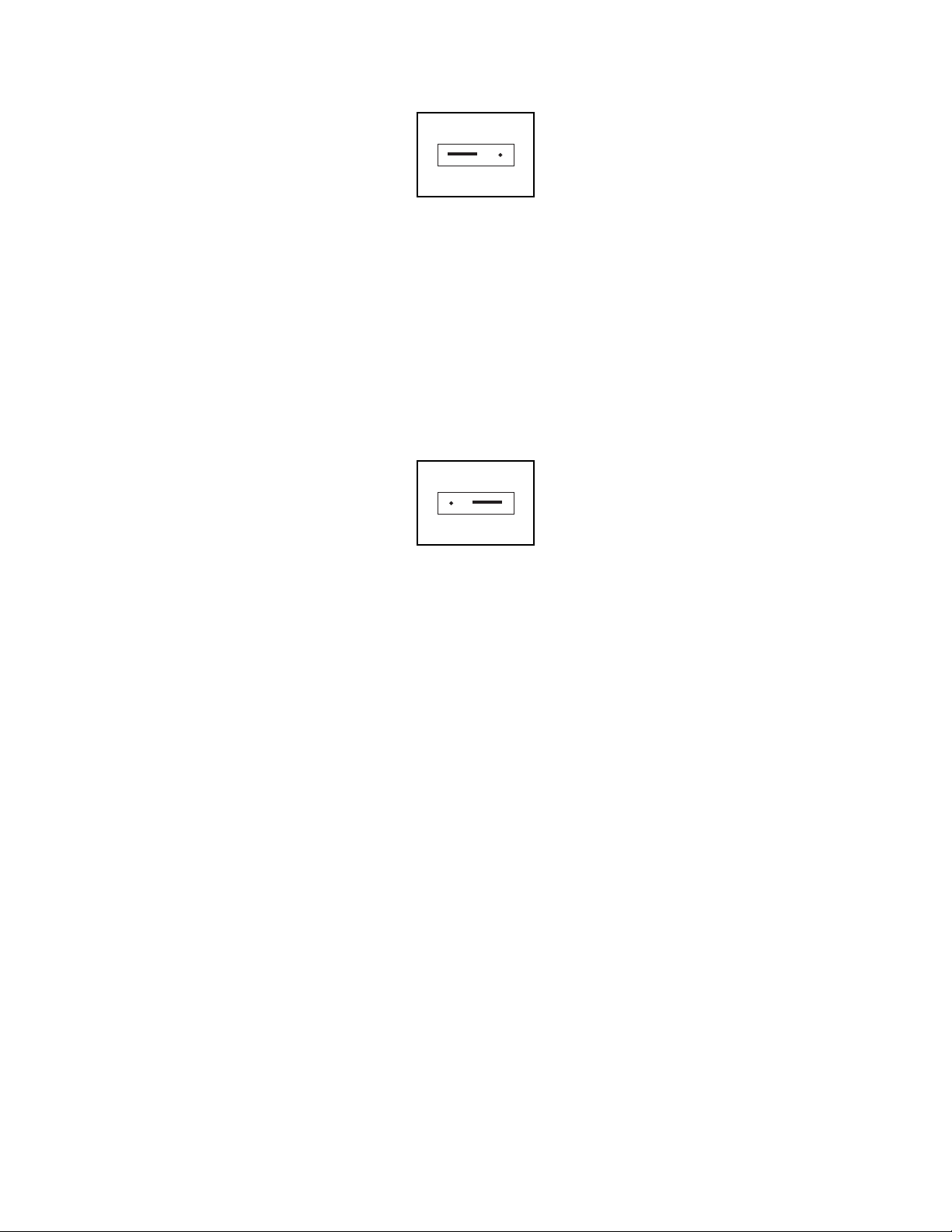
the board. The jumpers are shown in the parts locator diagram in Figure 2-1. Jumpers W1 and
W2 configure the two analog outputs. Jumper W3 (not labeled on the board) is used to select the
analog input range. Because of space constraints on the board, the jumper post labels are
missing. To distinguish between the A, B, and C posts of the jumpers, hold the board so that the
component side is facing you, the NuBus connector is down, and the 50-pin I/O connector is on
your right. The posts are then in the order A-B-C from left to right on all three of the horizontal
jumpers, as shown in Figure 2-1.
Note: This same orientation of the board is also assumed in the figures illustrating the
jumper connections (Figures 2-2 and 2-3).
© National Instruments Corporation 2-1 Lab-NB User Manual
Page 20
Configuration and Installation Chapter 2
3
2
1W1
2W2
3W3
1
Figure 2-1. Parts Locator Diagram
Lab-NB User Manual 2-2 © National Instruments Corporation
Page 21
Chapter 2 Configuration and Installation
Factory Default Jumper Settings
The Lab-NB is shipped from the factory with the following configuration:
• Jumpers W1 and W2–bipolar analog output
• Jumper W3–bipolar analog input
Table 2-1 lists all the available jumper configurations for the Lab-NB with the factory defaults
noted.
Table 2-1. Lab-NB Jumper Settings
Configuration Jumper Setting
Output CH0
Polarity
Output CH1
Polarity
Input Range Bipolar: ±5 V (factory setting)
Bipolar: ±5 V (factory setting)
Unipolar: 0 to 10 V
Bipolar: ±5 V (factory setting)
Unipolar: 0 to 10 V
Unipolar: 0 to 10 V
W1: A-B
W1: B-C
W2: A-B
W2: B-C
W3: A-B
W3: B-C
Analog Output Configuration
Two ranges are available for the analog outputs: bipolar (±5 V) and unipolar (0 to 10 V).
Jumper W1 controls output channel 0, and W2 controls output channel 1.
Bipolar Output Selection
You can select the bipolar (±5 V) output configuration for either analog output channel by
setting the following jumpers:
Analog Output Channel 0 W1 A-B
Analog Output Channel 1 W2 A-B
This configuration is shown in Figure 2-2.
© National Instruments Corporation 2-3 Lab-NB User Manual
Page 22
Configuration and Installation Chapter 2
W1
ABC
W2
ABC
Channel 0
Channel 1
Figure 2-2. Bipolar Output Jumper Configuration
Unipolar Output Selection
You can select the unipolar (0 to 10 V) output configuration for either analog output channel by
setting the following jumpers:
Analog Output Channel 0 W1 B-C
Analog Output Channel 1 W2 B-C
This configuration is shown in Figure 2-3.
W1
ABC
W2
ABC
Channel 0
Channel 1
Figure 2-3. Unipolar Output Jumper Configuration
Analog Input Configuration
Two ranges are available for the analog inputs: bipolar (±5 V) and unipolar (0 to 10 V). Jumper
W3 controls the input range for all eight analog input channels.
Bipolar Input Selection
You can select the bipolar (±5 V) input configuration by setting the following jumper:
Analog Input W3 A-B
This configuration is shown in Figure 2-4.
Lab-NB User Manual 2-4 © National Instruments Corporation
Page 23
Chapter 2 Configuration and Installation
W3
ABC
Figure 2-4. Bipolar Input Jumper Configuration
Unipolar Input Selection
You can select the unipolar (0 to 10 V) input configuration by setting the following jumper:
Analog Input W3 B-C
This configuration is shown in Figure 2-5.
W3
ABC
Figure 2-5. Unipolar Input Jumper Configuration
Note: If you are using a software package such as NI-DAQ or LabVIEW, you may need to
reconfigure your software to reflect any changes in jumper or switch settings.
Installation
Find the section in your Macintosh documentation that explains how to install an expansion
board in your computer. You can use this procedure as a universal board installation guide.
First, read the entire procedure. Then, install your Lab-NB board in the Macintosh by following
the outlined procedure.
Signal Connections
I/O Connector Pin Description
Figure 2-6 shows the pin assignments for the Lab-NB I/O connector. This connector is located
on the back panel of the Lab-NB board and is accessible at the rear of the Macintosh computer
after the board has been properly installed.
© National Instruments Corporation 2-5 Lab-NB User Manual
Page 24
Configuration and Installation Chapter 2
Warning: Connections that exceed any of the maximum ratings of input or output signals on
the Lab-NB may result in damage to the Lab-NB board and to the Macintosh
computer. This includes connecting any power signals to ground and vice versa.
National Instruments is
NOT liable for any damages resulting from any such
signal connections.
ACH0
ACH2
ACH4
ACH6
AIGND
AOGND
DGND
PA1
PA3
PA5
PA7
PB1
PB3
PB5
PB7
PC1
PC3
12
34
56
78
9
10
11 12
13 14
15 16
17 18
19 20
21 22
23 24
25 26
27 28
29 30
31 32
33 34
ACH1
ACH3
ACH5
ACH7
DAC0 OUT
DAC1 OUT
PA0
PA2
PA4
PA6
PB0
PB2
PB4
PB6
PC0
PC2
PC4
PC5
PC7
EXTUPDATE*
OUTB0
OUTB1
CLKB1
GATB2
+5V
35 36
37 38
39 40
41 42
43 44
45 46
47 48
49 50
PC6
EXTTRIG
EXTCONV*
GATB0
GATB1
OUTB2
CLKB2
DGND
Figure 2-6. Lab-NB I/O Connector Pin Assignments
Lab-NB User Manual 2-6 © National Instruments Corporation
Page 25

Chapter 2 Configuration and Installation
Signal Connection Descriptions
Pin Signal Name Description
1-8 ACH<0..7> Analog input channels 0 through 7 (single-ended).
9 AIGND Analog input ground.
10 DAC0 OUT Voltage output signal for analog output channel 0.
11 AOGND Analog output ground.
12 DAC1 OUT Voltage output signal for analog output channel 1.
13 DGND Digital ground.
14–21 PA<0..7> Bidirectional data lines for port A. PA7 is the MSB, PA0 the LSB.
22–29 PB<0..7> Bidirectional data lines for port B. PB7 is the MSB, PB0 the LSB.
30–37 PC<0..7> Bidirectional data lines for port C. PC7 is the MSB, PC0 the LSB.
38 EXTTRIG External control signal to start a timed conversion sequence.
39 EXTUPDATE* External control signal to update DAC outputs.
40 EXTCONV* External control signal to trigger A/D conversions.
41 OUTB0 Counter B0 output.
42 GATB0 Counter B0 gate.
43 OUTB1 Counter B1 output.
44 GATB1 Counter B1 gate.
45 CLKB1 Counter B1 clock.
46 OUTB2 Counter B2 output.
47 GATB2 Counter B2 gate.
48 CLKB2 Counter B2 clock.
49 +5 V +5 V out, 1 A maximum.
50 DGND Digital ground.
Note: Pin 49 is connected to the NuBus +5 V supply via a 1 A fuse. A replacement fuse is available
from Allied Electronics, part number 845-2007, and Littelfuse, part number 251001.
* Indicates that the signal is active low.
The connector pins can be grouped into analog input signal pins, analog output signal pins,
digital I/O signal pins, and timing I/O signal pins. Signal connection guidelines for each of these
groups are included later in this chapter.
Analog Input Signal Connections
Pins 1 through 8 are analog input signal pins for the 12-bit ADC. Pin 9, AIGND, is an analog
common signal. This pin can be used for a general analog power ground tie to the Lab-NB. Pins
1 through 8 are tied to the eight single-ended analog input channels of the input multiplexer
through 4.7-kΩ series resistances. Pin 40 is EXTCONV* and can be used to trigger conversions.
A conversion occurs when this signal makes a high-to-low transition. It can only be used to
© National Instruments Corporation 2-7 Lab-NB User Manual
Page 26
Configuration and Installation Chapter 2
cause conversions to occur; it cannot be used as a monitor to detect conversions caused by the
onboard sample-interval timer.
The following input ranges and maximum ratings apply to inputs ACH<0..7>:
Input impedance 0.1 GΩ in parallel with 45 pF
Input signal range Bipolar input: ±(5 / gain) V
Unipolar input: 0 to (10 / gain) V
Maximum input voltage rating ±45 V powered on or off
Exceeding the input signal range for gain settings greater than 1 will not damage the input
circuitry as long as the maximum input voltage rating of ±45 V is not exceeded. For example,
with a gain of 10, the input signal range is ±0.5 V for bipolar input and 0 to 1 V for unipolar
input, but the Lab-NB is guaranteed to withstand inputs up to the maximum input voltage rating.
Warning: Exceeding the input signal range will result in distorted input signals. Exceeding
the maximum input voltage rating may result in damage to the Lab-NB board and
to the Macintosh computer. National Instruments is
NOT liable for any damages
resulting from any such signal connections.
Connections for Signal Sources
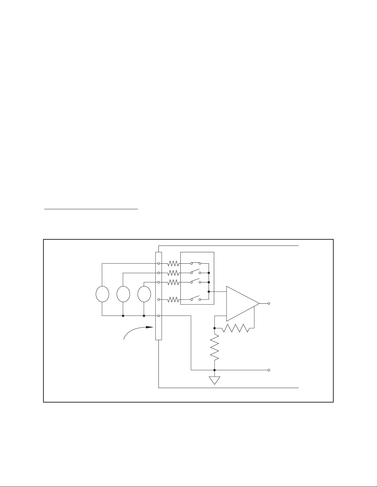
Figure 2-7 shows how to connect a signal source to a Lab-NB board. When you connect
grounded signal sources, observe the polarity carefully to avoid shorting the signal source output.
ACH<0..7>
•
•
•
Input Multiplexer
AIGND
+
-
R
f
R
a
Programmable Gain
Amplifier
+
M
Measured
-
V
Voltage
Signal
Source
+++
S1
V
V
I/O Connector
S2
V
S3
1
2
3
8
--9
Lab-NB Board
Figure 2-7. Analog Input Signal Connections
Lab-NB User Manual 2-8 © National Instruments Corporation
Page 27
Chapter 2 Configuration and Installation
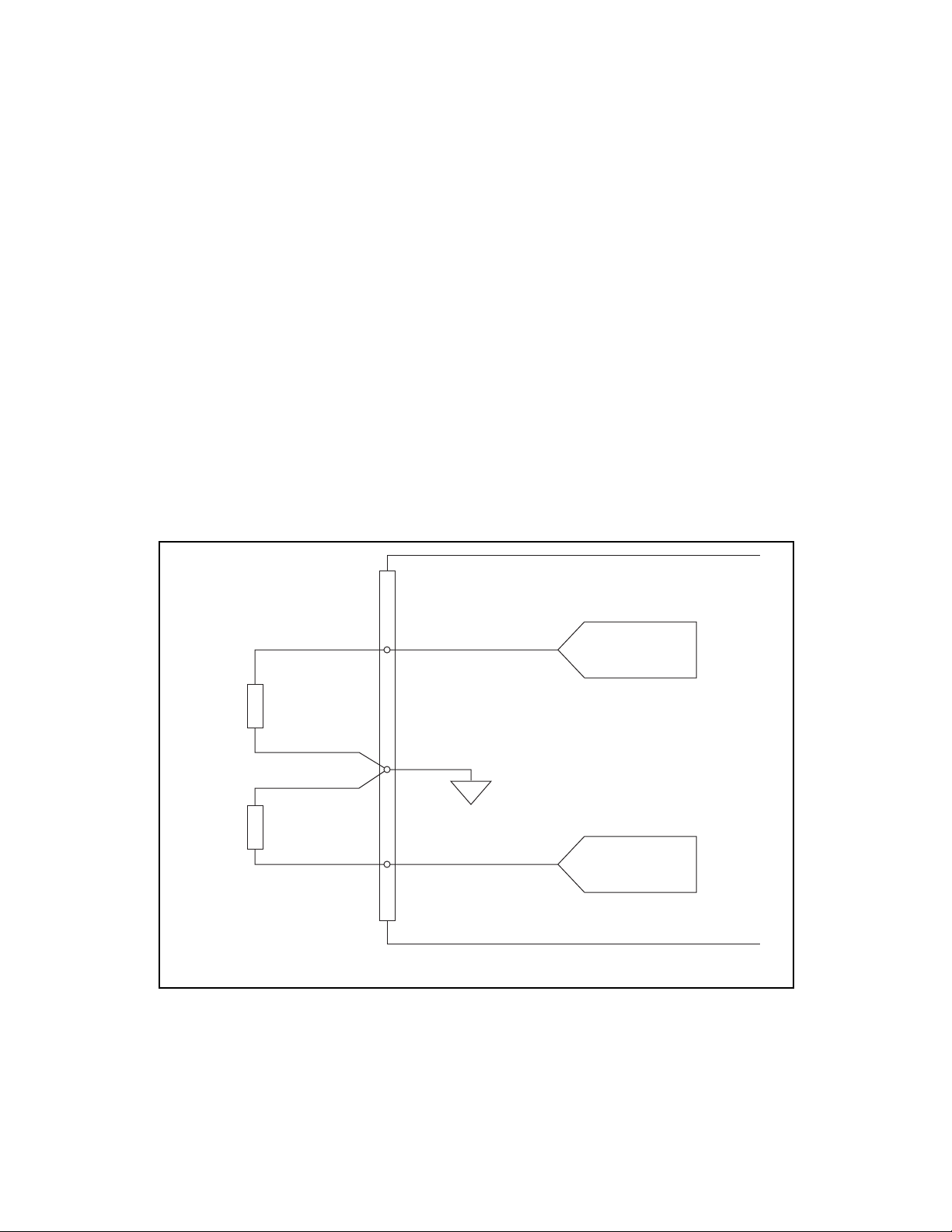
Analog Output Signal Connections
Pins 10 through 12 of the I/O connector are analog output signal pins.
Pins 10 and 12 are the DAC0 OUT and DAC1 OUT signal pins. DAC0 OUT is the voltage
output signal for Analog Output Channel 0. DAC1 OUT is the voltage output signal for Analog
Output Channel 1.
Pin 11, AOGND, is the ground reference point for both analog output channels as well as analog
input.
The following output ranges are available:
Output signal range Bipolar input: ±5 V
Unipolar input: 0 to 10 V
*
Maximum load current = ±1 mA for 12-bit linearity
Figure 2-8 shows how to make analog output connections.
DAC0 OUT10
+
Load
Load
VOUT 0
VOUT 1
-
-
+
11
12
AOGND
DAC1 OUT
*
*
Channel 0
Channel 1
Analog Output Channels
Lab-NB Board
Figure 2-8. Analog Output Signal Connections
© National Instruments Corporation 2-9 Lab-NB User Manual
Page 28

Configuration and Installation Chapter 2
Digital I/O Signal Connections
Pins 13 through 37 of the I/O connector are digital I/O signal pins. Digital I/O on the Lab-NB is
designed around the 82C55A integrated circuit. The 82C55A is a general-purpose PPI
containing 24 programmable I/O pins. These pins represent the three 8-bit ports (PA, PB, and
PC) of the 82C55A.
Pins 14 through 21 are connected to the digital lines PA<0..7> for digital I/O port A. Pins 22
through 29 are connected to the digital lines PB<0..7> for digital I/O port B. Pins 30 through 37
are connected to the digital lines PC<0..7> for digital I/O port C. Pin 13, DGND, is the digital
ground pin for all three digital I/O ports.
The following specifications and ratings apply to the digital I/O lines.
Absolute maximum voltage input rating +5.5 V with respect to DGND
-0.5 V with respect to DGND
Digital input specifications (referenced to DGND):
V
input logic high voltage 2.2 V min
IH
VIL input logic low voltage 0.8 V max
I
input current load,
IH
logic high input voltage 1.0 µA max
input current load,
I
IL
logic low input voltage -1.0 µA max
Digital output specifications (referenced to DGND):
output logic high voltage 3.7 V min
V
OH
VOL output logic low voltage 0.4 V max
I
output source current,
OH
logic high -2.5 mA max
output sink current,
I
OL
logic low 2.5 mA max
Lab-NB User Manual 2-10 © National Instruments Corporation
Page 29
Chapter 2 Configuration and Installation
Figure 2-9 illustrates signal connections for three typical digital I/O applications.
+5 V
LED
+5 V
Switch
I/O Connector
14 PA0
Port A
P A<7..0>
Port B
22 PB0
PB<7..0>
TTL Signal
30 PC0
Port C
PC<7..0>
13
DGND
Lab-NB Board
Figure 2-9. Digital I/O Connections
In Figure 2-9, port A is configured for digital output, and ports B and C are configured for digital
input. Digital input applications include receiving TTL signals and sensing external device states
such as the switch in Figure 2-9. Digital output applications include sending TTL signals and
driving external devices such as the LED shown in Figure 2-9.
Port C Pin Connections
The signals assigned to port C depend on the mode in which the 82C55A is programmed. In
mode 0, port C is considered as two 4-bit I/O ports. In modes 1 and 2, port C is used for status
and handshaking signals with two or three I/O bits mixed in. The following table summarizes
the signal assignments of port C for each programmable mode. See Chapter 4, Register-Level
Programming, for programming information.
Warning: During programming, note that each time a port is configured, output ports A
and C are reset to 0, and output port B is undefined.
© National Instruments Corporation 2-11 Lab-NB User Manual
Page 30
Configuration and Installation Chapter 2
Table 2-2. Port C Signal Assignments
Programming
Group A Group B
Mode
PC7 PC6 PC5 PC4 PC3 PC2 PC1 PC0
Mode 0
Mode 1 Input
Mode 1 Output
Mode 2
* Indicates that the signal is active low.
I/O I/O I/O I/O I/O I/O I/O I/O
I/O I/O IBF
OBFA* ACKA* I/O I/O INTR
OBFA* ACKA* IBF
STBA* INTR
A
STBA* INTR
A
STBB* IBFB
A
ACKB* OBFB* INTR
A
I/O I/O I/O
A
INTR
B
Timing Specifications
The handshaking lines STB* and IBF are used to synchronize input transfers. The handshaking
lines OBF* and ACK* are used to synchronize output transfers.
B
B
Lab-NB User Manual 2-12 © National Instruments Corporation
Page 31

Chapter 2 Configuration and Installation
The following signals are used in the timing diagrams shown later in this chapter:
Pin Direction Description
STB* Input Strobe Input—A low signal on this handshaking line loads data into the
input latch.
IBF Output Input Buffer Full—A high signal on this handshaking line indicates that
data has been loaded into the input latch. This is basically an input
acknowledge signal.
ACK* Input Acknowledge Input—A low signal on this handshaking line indicates
that the data written from the specified port has been accepted. This
signal is basically a response from the external device that it has received
the data from the Lab-NB.
OBF* Output Output Buffer Full—A low signal on this handshaking line indicates that
data has been written from the specified port.
INTR Output Interrupt Request—This signal becomes high when the 82C55A is
requesting service during a data transfer. The appropriate interrupt
enable signals must be set to generate this signal.
RD* Internal Read Signal—This signal is the read signal generated from the control
lines of the NuBus.
WR* Internal Write Signal—This signal is the write signal generated from the control
lines of the NuBus.
DATA Bidirectional Data Lines at the Specified Port—This signal indicates when the data on
the data lines at a specified port is or should be available.
© National Instruments Corporation 2-13 Lab-NB User Manual
Page 32

Configuration and Installation Chapter 2
Mode 1 Input Timing
The following figure illustrates the timing specifications for an input transfer in mode 1.
T1
T2
STB *
IBF
INTR
RD *
T3
DATA
T4
T6
T5
Name Description Minimum Maximum
T1 STB* pulse width 100 –
T2 STB* = 0 to IBF = 1 – 150
T3 Data before STB* = 1 20 –
T4 STB* = 1 to INTR = 1 – 150
T5 Data after STB* = 1 50 –
T6 RD* = 0 to INTR = 0 – 200
T7 RD* = 1 to IBF = 0 – 150
T7
All timing values are in nanoseconds.
© National Instruments Corporation 2-14 Lab-NB User Manual
Page 33

Chapter 2 Configuration and Installation
Mode 1 Output Timing
The following figure illustrates the timing specifications for an output transfer in mode 1.
T3
WR*
T4
OBF*
INTR
ACK*
DATA
T1
T5
T2
T6
Name Description Minimum Maximum
T1 WR* = 0 to INTR = 0 – 250
T2 WR* = 1 to output – 200
T3 WR* = 1 to OBF* = 0 – 150
T4 ACK* = 0 to OBF* = 1 – 150
T5 ACK* pulse width 100 –
T6 ACK* = 1 to INTR = 1 – 150
All timing values are in nanoseconds.
© National Instruments Corporation 2-15 Lab-NB User Manual
Page 34

Configuration and Installation Chapter 2
Mode 2 Bidirectional Timing
The following figure illustrates the timing specifications for bidirectional transfers in mode 2.
T1
WR *
T6
OBF *
INTR
ACK *
STB *
IBF
RD *
DATA
T3
T4
T2
T5
T7
T8
Name Description Minimum Maximum
T1 WR* = 1 to OBF* = 0 – 150
T2 Data before STB* = 1 20 –
T3 STB* pulse width 100 –
T4 STB* = 0 to IBF = 1 – 150
T5 Data after STB* = 1 50 –
T6 ACK* = 0 to OBF = 1 – 150
T7 ACK* pulse width 100 –
T8 ACK* = 0 to output – 150
T9 ACK* = 1 to output float 20 250
T10 RD* = 1 to IBF = 0 – 150
T10
T9
All timing values are in nanoseconds.
Lab-NB User Manual 2-16 © National Instruments Corporation
Page 35

Chapter 2 Configuration and Installation
Timing Connections
Pins 38 through 48 of the I/O connector are connections for timing I/O signals. The timing I/O of
the Lab-NB is designed around the 8253 Counter/Timer integrated circuit. Two of these integrated
circuits are employed in the Lab-NB. One, designated 8253(A), is used exclusively for DAQ
timing, and the other, 8253(B), is available for general use. Pins 38 through 40 carry external
signals that can be used for DAQ timing in place of the dedicated 8253(A). These signals are
explained under DAQ Timing Connections later in this chapter. Pins 41 through 48 carry generalpurpose timing signals from 8253(B). These signals are explained under General-Purpose
Timing Connections later in this chapter.
DAQ Timing Connections
Counter 0 on the 8253(A) Counter/Timer (referred to as A0) is used as a sample-interval counter
in timed A/D conversions. Counter 1 on the 8253(B) Counter/Timer (referred to as A1) is used as
a sample counter in conjunction with counter 0 for data acquisition. These counters are not
available for general use. In addition to counter A0, EXTCONV* can be used to externally time
conversions. See Chapter 4, Register-Level Programming, for the programming sequence needed
to enable this input. Figure 2-10 shows the timing requirements for the EXTCONV* input. An
A/D conversion is initiated by a falling edge on the EXTCONV*. If EXTCONV* stays low
more than 12
following rising edge on EXTCONV*. If EXTCONV* stays low less than 12
this conversion is latched into the FIFO memory after 12
µsec, the data from this conversion is not latched into the FIFO memory until the
µsec, the data from
µsec.
t
EXTCONV*
V
IH
V
IL
t
w
A/D Conversion starts within
125 nsec from this point
w
tw 250 nsec minimum
(worst-case)
(100 nsec typical)
Figure 2-10. EXTCONV* Signal Timing
Another external control, EXTTRIG, is used for either starting a DAQ sequence or terminating an
ongoing DAQ sequence, depending on the settings of the EXTTRIGEN and PRETRIG bits in the
ADC Configuration Register.
If EXTTRIGEN is set, EXTTRIG serves as an external trigger to start a DAQ sequence. In this
mode, posttrigger mode, the sample-interval counter is gated off until a rising edge is sensed on
the EXTTRIG line. EXTCONV*, however, is enabled on the first rising edge of EXTCONV*,
following the rising edge on the EXTTRIG line. Further transitions on the EXTTRIG line have no
© National Instruments Corporation 2-17 Lab-NB User Manual
Page 36

Configuration and Installation Chapter 2
effect until a new DAQ sequence is established. Figures 2-11 and 2-12 illustrate two possible
posttrigger DAQ timing cases. In Figure 2-11, the rising edge on EXTTRIG is sensed when the
EXTCONV* input is high. Thus, the first A/D conversion occurs on the second falling edge of
EXTCONV*, after the rising edge on EXTTRIG. In Figure 2-12, the rising edge on EXTTRIG is
sensed when the EXTCONV* input is low. In this case, the first A/D conversion occurs on the
first falling edge of EXTCONV*, after the rising edge on EXTTRIG. Notice that Figures 2-11
and 2-12 show a controlled acquisition mode DAQ sequence; that is, Sample Counter A1 disables
further A/D conversions after the programmed count (3 in the examples shown in Figures 2-11
and 2-12) expires. The counter is not loaded with the programmed count until the first falling edge
following a rising edge on the clock input; therefore two extra conversion pulses are generated as
shown in Figures 2-11 and 2-12. EXTTRIG can also be used as an external trigger in freerun
acquisition mode.
t
w
V
IH
EXTTRIG
EXTCONV*
V
IL
t
w
tw 50 nsec minimum
CONVERT
Sample
Counter
EXTTRIG
EXTCONV*
CONVERT
Sample
Counter
XX3210
Figure 2-11. Posttrigger DAQ Timing
(EXTCONV* High When Trigger Sensed)
t
w
V
IH
V
IL
t
w
tw 50 nsec minimum
td 50 nsec minimum
X 3210
Figure 2-12. Posttrigger DAQ Timing
(EXTCONV* Low When Trigger Sensed)
Lab-NB User Manual 2-18 © National Instruments Corporation
Page 37

Chapter 2 Configuration and Installation
If PRETRIG is set, EXTTRIG serves as a pretrigger signal. In pretrigger mode, A/D conversions
are enabled via software before a rising edge is sensed on the EXTTRIG input. However, the
sample counter, counter A1, is not gated on until a rising edge is sensed on the EXTTRIG input.
Additional transitions on this line have no effect until a new DAQ sequence is set up.
Conversions remain enabled for the programmed count after the trigger; therefore, data can be
acquired before and after the trigger. Pretrigger mode works only in controlled acquisition
mode, that is, counter A1 is required to disable A/D conversions after the programmed count
expires. Thus, the maximum number of samples acquired after the trigger is limited to 65,535.
The number of samples acquired before the trigger is limited only by the size of the memory
buffer available for data acquisition. Figure 2-13 shows a pretrigger DAQ timing sequence.
t
w
V
EXTTRIG
EXTCONV*
IH
V
IL
t
w
tw 50 nsec minimum
CONVERT
Sample
Counter
4
3210
Figure 2-13. Pretrigger DAQ Timing
Because both pretrigger and posttrigger modes use EXTTRIG input, only one mode can be used
at a time. If neither PRETRIG nor EXTTRIGEN is set high, this signal has no effect.
The final external control signal, EXTUPDATE*, is used to externally control the updating of
the output voltage of the 12-bit DACs or to generate an externally timed interrupt on the NuBus.
If the TMRWGEN bit in the DAC Configuration Register is set, the DAC voltage is updated by a
low level on the EXTUPDATE* signal. If the TMRINTEN bit in the Interrupt Control Register
is set, an interrupt is generated whenever a rising edge is detected on the EXTUPDATE* bit .
Therefore, externally timed, interrupt-driven waveform generation is possible on the Lab-NB.
Figure 2-14 illustrates a waveform generation timing sequence using the EXTUPDATE* signal.
Notice that the DACs are updated by a low level on the EXTUPDATE* line. Any writes to the
DAC Data Registers while EXTUPDATE* is low therefore result in immediate update of the
DAC output voltages.
© National Instruments Corporation 2-19 Lab-NB User Manual
Page 38

Configuration and Installation Chapter 2
EXTUPDATE*
DAC OUTPUT
UPDATE
TMRINTUP
DACWRT
t
ext
t
Minimum 50 nsec
ext
Figure 2-14. Waveform Generation Timing with the EXTUPDATE* Signal
Since a rising edge on the EXTUPDATE* signal always sets the TMRINTUP bit in the Interrupt
Status Register, the EXTUPDATE* signal can also be used for periodic interrupt generation
timed by an external source. The TMRINTUP bit is cleared by writing to either of the two
DACs or to the TMRINTCL bit location. Figure 2-15 illustrates a timing sequence where
EXTUPDATE* is being used to generate a NuBus interrupt.
EXTUPDATE*
TMRINTUP
and
NuBusNMR
TMRINTCLR
Figure 2-15. NuBus Interrupt Generation with the EXTUPDATE* Signal
The following specifications and ratings apply to the EXTCONV*, EXTTRIG and
EXTUPDATE* signals.
Absolute maximum voltage input rating -0.5 to 7.0 V with respect to DGND
Lab-NB User Manual 2-20 © National Instruments Corporation
Page 39

Chapter 2 Configuration and Installation
8253 digital input specifications (referenced to DGND):
input logic high voltage 2.2 V min
V
IH
V
input logic low voltage 0.8 V max
IL
Input load current ±10 µA max
8253 digital output specifications (referenced to DGND):
output logic high voltage 2.4 V min
V
OH
V
output logic low voltage 0.45 V max
OL
I
output source current, at V
OH
I
output sink current, at V
OL
OH
OL
400 µA max
2.2 mA max
General-Purpose Timing Signal Connections
The general-purpose timing signals include the GATE, CLK, and OUT signals for the three
8253(B) counters. The 8253 Counter/Timers can be used for general-purpose applications such
as pulse and square wave generation; event counting; and pulse-width, time-lapse, and frequency
measurement. For these applications, CLK and GATE signals are sent to the counters, and the
counters are programmed for various operations. The single exception is counter B0, which has
an internal 2-MHz clock.
The 8253 Counter/Timer is described briefly in Chapter 3, Theory of Operation
. For detailed
programming information, consult Appendix C, AMD 8253 Data Sheet.
Pulse and square wave generation are performed by programming a counter to generate a timing
signal at its OUT output pin.
Event counting is performed by programming a counter to count rising or falling edges applied
to any of the 8253 CLK inputs. The counter value can then be read to determine the number of
edges that have occurred. Counter operation can be gated on and off during event counting.
Figure 2-16 shows connections for a typical event-counting operation where a switch is used to
gate the counter on and off.
© National Instruments Corporation 2-21 Lab-NB User Manual
Page 40

Configuration and Installation Chapter 2
+5 V
4.7 kΩ
CLK
OUT
GATE
Switch
Signal
Source
Counter (from Group B)
13
I/O Connector
DGND
Lab-NB Board
Figure 2-16. Event-Counting Application with External Switch Gating
Pulse-width measurement is performed by level gating. The pulse to be measured is applied to
the counter GATE input. The counter is loaded with the known count and is programmed to
count down while the signal at the GATE input is high. The pulse width equals the counter
difference (loaded value minus read value) multiplied by the CLK period.
Time-lapse measurement is performed by programming a counter to be edge gated. An edge is
applied to the counter GATE input to start the counter. The counter can be programmed to start
counting after receiving a low-to-high edge. The time lapse since receiving the edge equals the
counter value difference (loaded value minus read value) multiplied by the CLK period.
Frequency measurement is performed by programming a counter to be level gated and by
counting the number of falling edges in a signal applied to a CLK input. The gate signal applied
to the counter GATE input is of known duration. In this case, the counter is programmed to
count falling edges at the CLK input while the gate is applied. The frequency of the input signal
then equals the count value divided by the gate period. Figure 2-17 shows the connections for a
frequency measurement application. A second counter could also be used to generate the gate
signal in this application.
Lab-NB User Manual 2-22 © National Instruments Corporation
Page 41

Chapter 2 Configuration and Installation
+5 V
4.7 kΩ
CLK
OUT
GATE
Signal
Source
I/O Connector
Gate
Source
13
Counter
DGND
Lab-NB Board
Figure 2-17. Frequency Measurement Application
The GATE, CLK, and OUT signals for counters B1 and B2 are available at the I/O connector. In
addition, the GATE and CLK pins are pulled up to +5 V through a 4.7 kΩ resistor. The input
and output ratings and timing specifications for the 8253 signals are given next.
The following specifications and ratings apply to the 8253 I/O signals:
Absolute maximum voltage input rating -0.5 to 7.0 V with respect to DGND
8253 digital input specifications (referenced to DGND):
input logic high voltage 2.2 V min
V
IH
V
input logic low voltage 0.8 V max
IL
Input load current ±10 µA max
8253 digital output specifications (referenced to DGND):
output logic high voltage 2.4 V min
V
OH
V
output logic low voltage 0.45 V max
OL
I
output source current, at V
OH
I
output sink current, at V
OL
© National Instruments Corporation 2-23 Lab-NB User Manual
OH
OL
400 µA max
2.2 mA max
Page 42

Configuration and Installation Chapter 2
Figure 2-18 shows the timing requirements for the GATE and CLK input signals and the timing
specifications for the OUT output signals of the 8253.
CLK
GATE
OUT
t
sc
V
IH
V
IL
t
gsu
V
IH
V
IL
t
outg
V
OH
V
OL
t
sc
t
pwh
t
pwl
t
gsu
t
gh
t
gwh
t
gwl
t
outg
t
outc
clock period
clock high level
clock low level
gate setup time
gate hold time
gate high level
gate low level
output delay from clock
output delay from gate
t
gwh
t
pwh
t
gh
380 nsec min
230 nsec min
150 nsec min
100 nsec min
50 nsec min
150 nsec min
100 nsec min
300 nsec min
400 nsec min
t
outc
t
pwl
t
gwl
Figure 2-18. General-Purpose Timing Signals
The GATE and OUT signals in Figure 2-18 are referenced to the rising edge of the CLK signal.
Lab-NB User Manual 2-24 © National Instruments Corporation
Page 43

Chapter 3 Theory of Operation
This chapter contains a functional overview of the Lab-NB and explains the operation of each
functional unit making up the Lab-NB.
Functional Overview
The block diagram in Figure 3-1 shows a functional overview of the Lab-NB board.
Data/
Address
16
FIFO
12-Bit
A/D
Pgm
Gain
Input
Max
8
NuBus
Control
Signals
NuBus
Interface
10-MHz
Clock
12
8253
Ctr/Timer
Group A
1-MHz
Timebase
÷ 10
÷ 5
82C55A
Digital
Interface
8
2-MHz
Timebase
Figure 3-1. Lab-NB Block Diagram
12
12
12-Bit
D/A
12-Bit
D/A
8253
Ctr/Timer
Group B
1
1
Back Panel Connector
© National Instruments Corporation 3-1 Lab-NB User Manual
Page 44

Theory of Operation Chapter 3
The following are the major components making up the Lab-NB board:
• NuBus interface circuitry
• Analog input and DAQ circuitry
• Analog output circuitry
• Digital I/O circuitry
• Timing I/O circuitry
DAQ functions can be executed by using the analog input circuitry and some of the timing I/O
circuitry. The internal data and control buses interconnect the components. The theory of
operation for each of these components is explained in the remainder of this chapter. The theory
of operation for the DAQ circuitry is included with the discussion of the analog input circuitry.
NuBus Interface Circuitry
The Macintosh NuBus is a 32-bit multiplexed address and data bus with a 10-MHz bus clock. In
addition, the NuBus provides interface signals for interrupt and read/write operations. The
NuBus interface circuitry consists of a starting address detector, interface timing signals, and
address-decoder circuitry. This interface circuitry generates the signals necessary to control and
monitor the operation of the Lab-NB multifunction circuitry.
AD<0..31>
16 16
10-MHz Clock
NuBus
÷ 10
Data
Transceivers
Address
Decoder
NuBus
Interface
Timing
1-MHz
Timebase
Internal Data Bus
Register Selects
Read & Write Signals
1-MHz Clock
(to 8253s)
÷ 5
2-MHz
Timebase
2-MHz Clock
(to 8253s)
Figure 3-2. NuBus Interface Circuitry Block Diagram
Lab-NB User Manual 3-2 © National Instruments Corporation
Page 45

Chapter 3 Theory of Operation
The starting-address-detecting circuitry on the Lab-NB matches address lines 23 through 21 to
the starting address specified by the slot in which the Lab-NB board is installed. The remaining
address lines (19 through 0) are decoded by the Lab-NB address-decoding circuitry to generate
select signals for the registers on the board. The NuBus interface timing signals are decoded by
the Lab-NB interface timing circuitry, which generates the proper read and write signals for the
remaining Lab-NB circuitry. The Lab-NB board can cause interrupts in the Macintosh by
driving the NuBus NMRQ* interrupt line.
Analog Input and DAQ Circuitry
The Lab-NB provides eight channels of analog input with software-programmable gain and
12-bit A/D conversion. Using the timing circuitry, the Lab-NB can also automatically time
multiple A/D conversions. Figure 3-3 shows a block diagram of the analog input and DAQ
circuitry.
ACH0
ACH1
ACH2
ACH3
ACH4
ACH5
ACH6
ACH7
EXT
TRIG
EXT
CONV*
Mux
I/O Connector
MUX
OUT
Programmable
Gain Amp
3
External Trigger
Mux
Counter
MUX CTR CLK
Sampleand-Hold
Amp
GAIN0
GAIN1
GAIN2
4
Convert
Data
Acquisition
Timing
ADC
ADC
Configuration
Register
A/D
Data
12
Counter/Timer
Signals
A/D
FIFO
ADC WR
Data
12
A/D
RD
CONV
AVAIL
Data
16
NuBus
Figure 3-3. Analog Input and DAQ Circuitry Block Diagram
© National Instruments Corporation 3-3 Lab-NB User Manual
Page 46

Theory of Operation Chapter 3
Analog Input Circuitry
The analog input circuitry consists of an input multiplexer, a software-programmable gain
amplifier, a 12-bit ADC, and a 12-bit FIFO memory that is sign-extended to 16 bits.
The input multiplexer is made up of a CMOS analog input multiplexer and has eight analog input
channels (channels 0 through 7). The input multiplexers provide input overvoltage protection of
±45 V, powered on or off.
The programmable gain amplifier applies gain to the input signal, allowing an input analog
signal to be amplified before being sampled and converted, thus increasing measurement
resolution and accuracy. The gain of the instrumentation amplifier is selected under software
control. The Lab-NB board provides gains of 1, 2, 5, 10, 20, 50, and 100.
The Lab-NB uses a 12-bit successive-approximation ADC. The 12-bit resolution of the
converter allows the converter to resolve its input range into 4,096 different steps. This
resolution also provides a 12-bit digital word that represents the value of the input voltage level
with respect to the converter input range. The ADC itself has a single input range of 0 to +5 V.
Additional circuitry allows inputs of ±5 V or 0 to 10 V.
When an A/D conversion is complete, the ADC clocks the result into the A/D FIFO. The A/D
FIFO is 16 bits wide and 16 words deep. This FIFO serves as a buffer to the ADC and provides
two benefits. First, any time an A/D conversion is complete, the value is saved in the A/D FIFO
for later reading, and the ADC is free to start a new conversion. Secondly, the A/D FIFO can
collect up to 16 A/D conversion values before any information is lost, thus allowing software
some extra time (16 times the sample interval) to catch up with the hardware. If more than 16
values are stored in the A/D FIFO without the A/D FIFO being read from, an error condition
called A/D FIFO Overflow occurs and A/D conversion information is lost.
The A/D FIFO generates a signal that indicates when it contains A/D conversion data. The state
of this signal can be read from the Lab-NB Status Register.
The output from the ADC can be interpreted as either straight binary or two's complement,
depending on which input mode you select (unipolar or bipolar). In unipolar mode, the data
from the ADC is interpreted as a 12-bit straight binary number with a range of 0 to +4,095. In
bipolar mode, the data from the ADC is interpreted as a 12-bit two's complement number with a
range of -2,048 to +2,047. In this mode, the MSB of the ADC result is inverted to make it two's
complement. The output from the ADC is then sign-extended to 16 bits, causing either a leading
0 or a leading F (hex) to be added, depending on the coding and the sign. Thus, data values read
from the FIFO are 16 bits wide.
DAQ Timing Circuitry
A DAQ operation refers to the process of taking a sequence of A/D conversions with the sample
interval (the time between successive A/D conversions) carefully timed. The DAQ timing
circuitry consists of various clocks and timing signals that perform this timing. Two types of
data acquisition can be performed by the Lab-NB board: single-channel data acquisition and
Lab-NB User Manual 3-4 © National Instruments Corporation
Page 47

Chapter 3 Theory of Operation
multichannel (scanned) data acquisition. Scanned data acquisition uses a counter to
automatically switch between analog input channels during data acquisition.
DAQ timing consists of signals that initiate a DAQ operation, initiate individual A/D
conversions, gate the DAQ operation, and generate scanning clocks. Sources for these signals
are supplied mainly by timers on the Lab-NB board. One of the two 8253 integrated circuits is
reserved for this purpose.
An A/D conversion can be initiated by a high-to-low transition on the counter A0 output
(OUT A0) of the 8253(A) Counter/Timer chip on the Lab-NB or by a high-to-low transition on
EXTCONV* input. During data acquisition, the onboard sample-interval counter–counter 0 of
8253(A)–is used to generate pulses that initiate A/D conversions.
The sample-interval timer is a 16-bit down counter that uses the 1-MHz clock onboard to
generate sample intervals from 2 µsec to 65,535 µsec (see Timing I/O Circuitry later in this
chapter). Alternatively, it can use the output from counter B0 (OUTB0) of the 8253(B)
Counter/Timer chip on the Lab-NB. Each time the sample-interval timer reaches 0, it generates
a pulse and reloads with the programmed sample-interval count. This operation continues until
the counter is reprogrammed.
As stated in Chapter 4, Register-Level Programming, only counter A0 is required for DAQ
operations in freerun acquisition mode. The software must keep track of the number of
conversions that has occurred and turn off counter A0 after the required number of conversions
has been obtained. In controlled acquisition mode, two counters (counters A0 and A1) are
required for a DAQ operation. Counter A0 generates the conversion pulses, and counter A1
gates off counter A0 after the programmed count has expired.
Single-Channel Data Acquisition
During single-channel data acquisition, the channel select and gain bits in the A/D Configuration
Register select the gain and analog input channel before data acquisition is initiated. These gain
and multiplexer settings remain constant during the entire DAQ process; therefore, all A/D
conversion data is read from a single channel.
Multichannel (Scanned) Data Acquisition
Multichannel data acquisition is performed by enabling scanning during data acquisition.
Multichannel scanning is controlled by a scan counter.
For scanning operations, the scan counter decrements from the highest numbered channel
(specified by the user) through channel 0 and then repeats the sequence. Thus, any number of
channels from 2 to 8 can be scanned. Notice that the same gain setting is used for all channels in
the scan sequence.
© National Instruments Corporation 3-5 Lab-NB User Manual
Page 48

Theory of Operation Chapter 3
DAQ Rates
Maximum DAQ rates (number of samples per second) are determined by the conversion period
of the ADC plus the sample-and-hold acquisition time. During multichannel scanning, the DAQ
rates are further limited by the settling time of the input multiplexers and programmable gain
amplifier. After the input multiplexers are switched, the amplifier must be allowed to settle to
the new input signal value to within 12-bit accuracy before an A/D conversion is performed, or
else 12-bit accuracy will not be achieved. The settling time is a function of the gain selected.
The Lab-NB DAQ timing circuitry detects when DAQ rates are high enough to cause A/D
conversions to be lost. If this is the case, this circuitry sets an Overrun error flag in the Lab-NB
Status Register. If the recommended DAQ rates in Table 3-2 are exceeded (an error flag is not
automatically set), the analog input circuitry may not perform at 12-bit accuracy. If these rates
are exceeded by more than a few microseconds, A/D conversions may be lost. Table 3-1 shows
the recommended multiplexer and gain settling times for different gain settings.
Table 3-2 shows the maximum recommended DAQ rates for both single-channel and
multichannel data acquisition. Notice that for a single-channel data acquisition, the data can be
acquired at the maximum rate at any gain setting. The analog input bandwidth, however, is
lower for higher gains. For multichannel data acquisition, observing the DAQ rates given in
Table 3-2 ensures 12-bit accuracy.
Table 3-1. Analog Input Settling Time Versus Gain
Gain Setting Settling Time Recommended
1 16 µsec
2, 5 20 µsec
10, 20 30 µsec
50, 100 100 µsec
Table 3-2. Lab-NB Maximum Recommended DAQ Rates
Single-Channel Data Acquisition:
Any Gain Setting 62.5 ksamples/sec
Multichannel Data Acquisition:
Gain = 1 62.5 ksamples/sec
Gain = 2, 5 50.0 ksamples/sec
Gain = 10, 20 33.3 ksamples/sec
Gain = 50, 100 10.0 ksamples/sec
Lab-NB User Manual 3-6 © National Instruments Corporation
Page 49

Chapter 3 Theory of Operation
The recommended DAQ rates given in Table 3-2 assume that voltage levels on all the channels
included in the scan sequence are within range for the given gain and are driven by lowimpedance sources. The signal ranges for the possible gains are shown in Table 3-3 and
Table 3-4. Signal levels outside the ranges shown in Table 3-3 on the channels included in the
scan sequence adversely affect the input settling time. Similarly, greater settling time may be
required for channels driven by high-impedance signal sources.
Table 3-3. Bipolar Analog Input Signal Range Versus Gain
Gain Setting Input Signal Range
1 -5 V to 4.99756 V
2 -2.5 V to 2.49878 V
5 -1.0 V to 0.99951 V
10 -500 mV to 499.756 mV
20 -250 mV to 249.877 mV
50 -100 mV to 99.951 mV
100 -50 mV to 49.975 mV
Table 3-4. Unipolar Analog Input Signal Range Versus Gain
Gain Setting Input Signal Range
1 0 V to 9.99756 V
2 0 V to 4.99878 V
5 0 V to 1.99951 V
10 0 mV to 999.756 mV
20 0 mV to 499.877 mV
50 0 mV to 199.951 mV
100 0 mV to 99.975 mV
Analog Output Circuitry
The Lab-NB provides two channels of 12-bit D/A output. Each analog output channel can
provide unipolar or bipolar output. Figure 3-4 shows a block diagram of the analog output
circuitry.
© National Instruments Corporation 3-7 Lab-NB User Manual
Page 50

Theory of Operation Chapter 3
TWOSDA0
DAC0WR
Coding
Data
12
DAC0
Ref
5 V Internal
Reference
DAC0 OUT
AGND
DAC1WR
NuBus Interface
Counter
A2
CNFGWR
Ref
Coding
TWOSDA1
TMRWGN1
DAC1
DAC Configuration
Register
TWOSDA1
TMRWGN0
DAC1 OUT
I/O Connector
EXTUPDATE*
TWOSDA0
Figure 3-4. Analog Output Circuitry Block Diagram
Each analog output channel contains a 12-bit DAC. The DAC in each analog output channel
generates a voltage proportional to the input voltage reference (V
) multiplied by the digital
ref
code loaded into the DAC. Each DAC can be loaded with a 12-bit digital code by writing to the
DAC0 and DAC1 Registers on the Lab-NB board. The voltage output from the two DACs is
available at the Lab-NB I/O connector DAC0 OUT and DAC1 OUT pins.
The DAC voltages can be updated in any of three ways, depending on the setting of the
TMRWGN bit. If this bit is cleared, the DAC output voltage is updated as soon as the
corresponding DAC Data Register is written to. If the TMRWGN bit is set, the DAC output
voltage does not change until a falling edge is detected either from counter A2 or from
EXTUPDATE*.
Each DAC channel can be jumper-programmed for either a unipolar voltage output or a bipolar
voltage output range. A unipolar output gives an output voltage range of 0.0000 V to +9.9976 V.
A bipolar output gives an output voltage range of -5.0000 V to +4.9976 V. For unipolar output,
0.0000 V output corresponds to a digital code word of 0. For bipolar output, -5.0000 V output
corresponds to a digital code word of F800 (hex). One LSB is the voltage increment
Lab-NB User Manual 3-8 © National Instruments Corporation
Page 51

Chapter 3 Theory of Operation
corresponding to an LSB change in the digital code word. For both unipolar and bipolar output,
one LSB corresponds to the following formula:
10 V
4,096
Digital I/O Circuitry
The digital I/O circuitry is designed around an 82C55A integrated circuit. The 82C55A is a
general-purpose PPI containing 24 programmable I/O pins. These pins represent the three 8-bit
I/O ports (A, B, and C) of the 82C55A as well as PA<0..7>, PB<0..7>, and PC<0..7> on the
Lab-NB I/O connector. The 82C55A also has a control register to configure each of the three
I/O ports on the chip. These ports can be programmed as two groups of 12 signals or as three
individual 8-bit ports. In addition, the board can be programmed in one of the three modes of
operation: basic I/O, strobed I/O, or bidirectional bus. The programming of the digital I/O
circuitry is covered in Chapter 4, Register-Level Programming.
NuBus
DATA<0..7>
DIO RD/WR
2
To
Interrupt
Control
82C55A
Programmable
Peripheral
Interface
PC0
PC3
PA<0..7>
8
PB<0..7>
8
PC<0..7>
8
I/O Connector
Figure 3-5. Digital I/O Circuitry Block Diagram
© National Instruments Corporation 3-9 Lab-NB User Manual
Page 52

Theory of Operation Chapter 3
All three ports on the 82C55A are TTL-compatible. When enabled, the digital output ports are
capable of sinking 2.5 mA of current and sourcing 2.5 mA of current on each digital I/O line.
When the ports are not enabled, the digital I/O lines act as high-impedance inputs.
Timing I/O Circuitry
The Lab-NB uses two 8253 Counter/Timer integrated circuits for DAQ timing and for generalpurpose timing I/O functions. One of these is used internally for DAQ timing, and the other is
available for general use. Figure 3-6 shows a block diagram of both groups of timing I/O
circuitry (counter groups A and B).
NuBus
CTR RD
CTR WR
Data
8
1-MHz Source
TBSEL
CLKA0
GATEA0
Sample
Interval
Counter
OUTA0
CLKA1
Sample
Counter
GATEA1
OUTA1
OUTB0
MUX
CLKB0
2-MHz
Source
A/D Conversion Logic
GATEB2
CLKB2
OUTB2
GATEB1
CLKB1
OUTB1
OUTB0
GATEB0
8253
Counter/Timer
Group B
EXTCONV*
I/O Connector
EXTTRIG
CLKA2
GATEA2
DAC
Timing
OUTA2
8253
Counter/Timer
Group A
+5 V
EXTUPDATE*
D/A Conversion Timing
Figure 3-6. Timing I/O Circuitry Block Diagram
Lab-NB User Manual 3-10 © National Instruments Corporation
Page 53

Chapter 3 Theory of Operation
Each 8253 contains three independent 16-bit counter/timers and one 8-bit Mode Register. As
shown in Figure 3-6, counter group A is reserved for DAQ timing, and counter group B is free
for general use. The output of counter B0 can be used in place of the 1-MHz clock source on
counter A0 to allow clock periods greater than 65,536 µsec. All six counter/timers can be
programmed to operate in several useful timing modes. The programming and operation of the
8253 is presented in detail both in Chapter 4, Register-Level Programming, and in Appendix C,
AMD 8253 Data Sheet.
The 8253 for counter group A uses either a 1-MHz clock generated from the NuBus clock or the
output from counter B0, which has a 2-MHz clock source, for its timebase. The timebases for
counters B1 and B2 must be supplied externally through the 50-pin I/O connector. The 16-bit
counters in the 8253 can be diagrammed as shown in Figure 3-7.
CLK
Counter
GATE
OUT
Figure 3-7. Counter Block Diagram
Each counter has a CLK input pin, a GATE input pin, and an output pin labeled OUT. The 8253
counters are numbered 0 through 2, and their GATE, CLK, and OUT pins are labeled GATE N,
CLK N, and OUT N, where N is the counter number.
© National Instruments Corporation 3-11 Lab-NB User Manual
Page 54

Chapter 4 Register-Level Programming
This chapter describes in detail the address and function of each of the Lab-NB control and status
registers. This chapter also includes important information about register-level programming the
Lab-NB.
Note: If you plan to use a programming software package such as NI-DAQ or LabVIEW
with your Lab-NB board, you need not read this chapter.
Register Access
The Macintosh uses memory mapping to access boards in the system. The following sections
discuss how to access the various registers on the Lab-NB.
Slot Address Space
Each slot in the Macintosh computer is allocated a block of Macintosh memory addresses known
as the slot address space. All I/O boards plugged into Macintosh slots are therefore memory
mapped, and when a board is plugged into a given slot, its registers can be accessed within that
slot address space. The block of memory addresses allocated to each slot depends on the slot
number. The slots are labeled 1 through 6 next to the slot connectors inside the Macintosh II,
IIx, and IIfx. Table 4-1 shows the slot address space for each slot.
© National Instruments Corporation 4-1 Lab-NB User Manual
Page 55

Register-Level Programming Chapter 4
Table 4-1. Macintosh Slot Addresses
Slot Number Starting Address (Hex) Ending Address (Hex)
24-Bit Mode
9 0090 0000 009F FFFF
A 00A0 0000 00AF FFFF
B 00B0 0000 00BF FFFF
C 00C0 0000 00CF FFFF
D 00D0 0000 00DF FFFF
E 00E0 0000 00EF FFFF
32-Bit Mode
0 F000 0000 F0FF FFFF
1 F100 0000 F1FF FFFF
2 F200 0000 F2FF FFFF
3 F300 0000 F3FF FFFF
4 F400 0000 F4FF FFFF
5 F500 0000 F5FF FFFF
6 F600 0000 F6FF FFFF
7 F700 0000 F7FF FFFF
8 F800 0000 F8FF FFFF
9 F900 0000 F9FF FFFF
A FA00 0000 FAFF FFFF
B FB00 0000 FBFF FFFF
C FC00 0000 FCFF FFFF
D FD00 0000 FDFF FFFF
E FE00 0000 FEFF FFFF
Register Map
The register map for the Lab-NB is given in Table 4-2. This table gives the register name, the
register address offset from the board’s base address, the type of the register (read only, write
only, or read and write), and the size of the register in bits.
The register addresses in Table 4-2 are the offset addresses from the slot starting address. To
calculate the absolute address of the register, add the slot starting address given in Table 4-1 to
the register offset given in Table 4-2. For example, if the Lab-NB is plugged into the third slot
(corresponding to slot starting address B0 0000), the ADC FIFO memory is at address B0 0000 +
0 8010, that is, address B0 8010.
Lab-NB User Manual 4-2 © National Instruments Corporation
Page 56

Chapter 4 Register-Level Programming
Table 4-2. Lab-NB Register Map
Offset
Register Name Address (Hex) Type Size
Analog Input Register Group
A/D Configuration Register 0 8000 Write-only 16-bit
Status Register 0 8000 Read-only 8-bit
A/D FIFO Register 0 8010 Read-only 16-bit
A/D Clear Register 0 8010 Write-only 8-bit
Analog Output Register Group
DAC Configuration Register 5 8000 Write-only 8-bit
DAC0 Data Register 5 8010 Write-only 16-bit
DAC1 Data Register 5 8020 Write-only 16-bit
DAC0 and DAC1 Data Registers 5 8030 Write-only 16-bit
8253 Counter/Timer Register Group A
Counter A0 Data Register 4 0000 Read-and-write 8-bit
Counter A1 Data Register 4 0010 Read-and-write 8-bit
Counter A2 Data Register 4 0020 Read-and-write 8-bit
Counter A Mode Register 4 0030 Write-only 8-bit
8253 Counter/Timer Register Group B
Counter B0 Data Register 4 8000 Read-and-write 8-bit
Counter B1 Data Register 4 8010 Read-and-write 8-bit
Counter B2 Data Register 4 8020 Read- and-write 8-bit
Counter B Mode Register 4 8030 Write-only 8-bit
82C55A Digital I/O Register Group
Port A Register 5 0000 Read-and-write 8-bit
Port B Register 5 0010 Read-and-write 8-bit
Port C Register 5 0020 Read-and-write 8-bit
Digital Control Register 5 0030 Write-only 8-bit
Interrupt Control Register Group
Interrupt Control Register 1 0000 Write-only 8-bit
Interrupt Status Register 1 0000 Read-only 8-bit
Timer Interrupt Clear Register 1 8000 Write-only 8-bit
© National Instruments Corporation 4-3 Lab-NB User Manual
Page 57

Register-Level Programming Chapter 4
Register Sizes
The Macintosh permits three different memory word sizes for memory read and write
operations–byte (8-bit), half-word (16-bit), and word (32-bit). Table 4-2 shows the word sizes of
the Lab-NB registers. For example, reading the A/D FIFO Register requires a 16-bit read
operation at the specified address.
Register Descriptions
Table 4-2 divides the Lab-NB registers into six different register groups. A bit description of
each of the registers making up these groups is included later in this chapter.
The Analog Input Register Group is used to read output from the 12-bit successiveapproximation ADC. The Analog Output Group accesses the two 12-bit DACs. The two
Counter/Timer Groups (A and B) are each made up of four registers—one group for each of the
two onboard 8253 Counter/Timer integrated circuits. The Digital I/O Register Group consists of
the four registers of the onboard 82C55A PPI integrated circuit used for digital I/O. The
Interrupt Control Register Group can be used to enable the interrupt facility on the Lab-NB
board.
Warning: During programming, note that each time a port is configured, output ports A
and C are reset to 0, and output port B is undefined.
Register Description Format
The remainder of this register description chapter discusses each of the Lab-NB registers in the
order shown in Table 4-2. Each register group is introduced, followed by a detailed bit
description of each register. The individual register description gives the address, type, word
size, and bit map of the register, followed by a description of each bit.
The register bit map shows a diagram of the register with the MSB (bit 15 for a 16-bit register,
bit 7 for an 8-bit register) shown on the left, and the LSB (bit 0) shown on the right. A square is
used to represent each bit. Each bit is labeled with a name inside its square. An asterisk (*) after
the bit name indicates that the bit is inverted (negative logic).
In many of the registers, several bits are labeled with an X, indicating don't care bits. When a
register is read, these bits may appear set or cleared but should be ignored because they have no
significance. When a register is written to, setting or clearing these bit locations has no effect on
the Lab-NB hardware.
The bit map field for some write-only registers states not applicable, no bits used. Writing to
these registers causes some event to occur on the Lab-NB, such as clearing the analog input
circuitry. The data is ignored when writing to these registers; therefore, any bit pattern will
suffice.
Lab-NB User Manual 4-4 © National Instruments Corporation
Page 58

Chapter 4 Register-Level Programming
Analog Input Register Group
The four registers making up the Analog Input Register Group control the analog input circuitry
and are used for reading from the A/D FIFO. The A/D Configuration Register selects the input
channel to be read, the gain for that channel, and some information about the input data. The
Status Register reports the status of the current A/D conversion and returns any errors found.
Reading the A/D FIFO Register returns stored A/D conversion results. Writing to this register
resets the error bits in the Status Register and empties the A/D FIFO. One garbage data byte is
stored in the FIFO as a result of the clear operation, so the FIFO must be read after an A/D clear
to remove this data byte before starting a new conversion.
Bit descriptions for the registers in the Analog Input Register Group are given on the following
pages.
© National Instruments Corporation 4-5 Lab-NB User Manual
Page 59

Register-Level Programming Chapter 4
A/D Configuration Register
The A/D Configuration Register indicates the input channel to be read and the gain for the
analog input circuitry.
Address: Base address + 0 8000 (hex)
Type: Write-only
Word Size: 16-bit
Bit Map:
15 14 13 12 11 10 9 8
X X X X X TBSEL EXTTRIGEN PRETRIG
76543210
SCANEN MA2 MA1 MA0 GAIN2 GAIN1 GAIN0 TWOSCMP
Bit Name Description
15–11 X Don’t care bits.
10 TBSEL Clock Select Bit—This bit is used to select the clock source for
A/D conversions. If this bit is cleared, an internal 1-MHz clock
drives the counter (counter A0), and the interval between samples
is the value loaded into counter A0 multiplied by 1 µsec. If this bit
is set, then the output of user-programmable counter B0 is used as
a clock source. The timebase for counter B0 is fixed at 2 MHz and
cannot be changed. The interval between acquired samples is the
value loaded into counter A0 multiplied by the period of the output
signal from counter B0.
9 EXTTRIGEN External Trigger Enable Bit—This bit is one of two bits that
determines the effect of the EXTTRIG signal on the 50-pin I/O
connector. The function of this bit depends on the setting of the
PRETRIG bit. If PRETRIG is set, then this bit has no effect in
either setting. If PRETRIG is cleared and EXTRIGEN is set, then
a rising edge on the EXTTRIG signal starts a sequence of A/D
conversions. Unlike the EXTCONV* line, which controls
individual conversions, EXTTRIG in this case can only start a
multiple A/D conversion DAQ operation with the sample period
determined by the value in counter A0. If both EXTTRIGEN and
PRETRIG are cleared, then the EXTTRIG line on the I/O
connector has no effect.
Lab-NB User Manual 4-6 © National Instruments Corporation
Page 60

Chapter 4 Register-Level Programming
Bit Name Description (continued)
8 PRETRIG Pretrigger Bit—This bit is used to set the pretriggering feature on
the Lab-NB. It also supersedes any setting in the EXTTRIGEN bit
described earlier. If PRETRIG is cleared, then the function of the
EXTTRIG line on the I/O connector is determined by
EXTTRIGEN. If PRETRIG is set, then the EXTTRIG line
becomes a pretrigger. In pretrigger operation, the sample counter
(counter A1) does not begin decrementing until a rising edge is
detected on EXTTRIG. When the conversion sequence terminates,
some of the acquired data has been received before the trigger
signal and some has arrived after the signal. The number of
samples after the trigger is the value loaded into the sample
counter (counter A1), but the number of samples before the trigger
depends on the arrival time of the trigger signal.
7 SCANEN Scan Enable Bit—This bit enables or disables multichannel
scanning during data acquisition. If this bit is set, analog channels
MA<2..0> through 0 are sampled alternately. If this bit is cleared,
a single analog channel specified by MA<2..0> is sampled during
the entire DAQ operation. See Programming Multiple A/D
Conversions with Channel Scanning later in this chapter for the
correct sequence involved in setting this bit. For example, if
MA<2..0> is 011 and SCANEN is set, analog input channels 3
through 0 are sampled alternately during subsequent data
conversions. If SCANEN is then cleared (with MA<2..0> still set
to 011), only analog input channel 3 is sampled during the
subsequent data conversions.
6–4 MA<2..0> Multiplexer Address Bit—These three bits select which of the
eight input channels are read. The analog input multiplexer
depends on these three bits to select the input channel. The input
channel is selected as follows:
MA<2..0> Selected Channel
000
001
010
011
100
101
110
111
0
1
2
3
4
5
6
7
If SCANEN is set, analog channels MA<2..0> through 0 are
sampled alternately. If SCANEN is cleared, a single analog
channel specified by MA<2..0> is sampled during the entire DAQ
operation. See Programming Multiple A/D Conversions with
© National Instruments Corporation 4-7 Lab-NB User Manual
Page 61

Register-Level Programming Chapter 4
Bit Name Description (continued)
Channel Scanning later in this chapter for the correct sequence
involved in setting the SCANEN bit.
3–1 GAIN<2..0> Gain Bit—These three bits select the gain setting as follows:
GAIN<2..0> Selected Gain
000
001
010
011
100
101
110
111
1
1.25
2
5
10
20
50
100
0 TWOSCMP Two’s Complement Bit—This bit selects the format of the coding
of the output of the ADC. If this bit is set, the 12-bit data from the
ADC is sign-extended to 16 bits. If this bit is cleared, bits
<15..12> return 0.
Lab-NB User Manual 4-8 © National Instruments Corporation
Page 62

Chapter 4 Register-Level Programming
Status Register
The Status Register indicates the status of the current A/D conversion. The bits in this register
determine if a conversion is being performed or if data is available and any errors have been
found.
Address: Base address + 0 8000 (hex)
Type: Read-only
Word Size: 8-bit
Bit Map:
76543 210
X X X GATA1 OVERRUN OVERFLOW GATA0 DAVAIL
Bit Name Description
7–5 X Don’t care bits.
4 GATA1 Gate 1 Input Status Bit—This bit indicates the status of the GATE
1 input on the counter/timer chip (counter group A).
3 OVERRUN Overrun Error Status Bit—This bit indicates if an overrun error has
occurred. If this bit is cleared, no error occurred. This bit is set if
a convert command is issued to the ADC while the last conversion
is still in progress.
2 OVERFLOW Overflow Error Status Bit—This bit indicates if an overflow error
has occurred. If this bit is cleared, no error was encountered. If
this bit is set, the A/D FIFO has overflowed because the DAQ
servicing operation could not keep up with the sampling rate.
1 GATA0 Gate 0 Input Status Bit—This bit indicates the status of the GATE
0 input on the counter/timer chip (counter group A). This bit can
be used as a busy indicator for DAQ operations because
conversions are enabled as long as GATE 0 is high and counter A0
is programmed appropriately.
0 DAVAIL Data Available Bit—This bit indicates whether conversion output
is available. If this bit is set, the ADC is finished with the last
conversion and the result can be read from the FIFO. This bit is
cleared if the FIFO is empty.
© National Instruments Corporation 4-9 Lab-NB User Manual
Page 63

Register-Level Programming Chapter 4
A/D FIFO Register
Reading the A/D FIFO Register returns the next A/D conversion value stored in the A/D FIFO.
Whenever the A/D FIFO Register is read, the value read is removed from the A/D FIFO, thereby
freeing space for another A/D conversion value to be stored. Values are stored into the A/D
FIFO Register by the ADC whenever an A/D conversion is complete. Although A/D conversion
values are in 12-bit format, they are automatically sign-extended to 16 bits in the FIFO.
The A/D FIFO is emptied when all values it contains are read. The Status Register should be
read before the A/D FIFO Register is read. If the A/D FIFO contains one or more A/D
conversion values, the DAVAIL bit is set in the Status Register, and the A/D FIFO Register can
be read to retrieve a value. If the DAVAIL bit is cleared, the A/D FIFO is empty, in which case
reading the A/D FIFO Register returns meaningless information.
The values returned by reading the A/D FIFO Register are available in two different binary
formats: straight binary or two's complement binary. The binary format used is selected by the
TWOSCMP bit in the A/D Configuration Register. The bit pattern returned for either format is
given below.
Address: Base address + 0 8010 (hex)
Type: Read-only
Word Size: 16-bit
Bit Map: Straight binary mode
15 14 13 12 11 10 9 8
0 0 0 0 D11 D10 D9 D8
76543210
D7 D6 D5 D4 D3 D2 D1 D0
Bit Name Description
15–0 D<15..0> Data Bit—These bits contain the straight binary result of a 12-bit
A/D conversion. Bits D<15..12> are always 0 in straight binary
mode. Values read, therefore, range from 0 to +4,095 decimal
(0000 to 0FFF hex). Straight binary mode is useful for unipolar
analog input readings because all values read reflect a positive
polarity input signal.
Lab-NB User Manual 4-10 © National Instruments Corporation
Page 64

Chapter 4 Register-Level Programming
A/D FIFO Register (continued)
Bit Map: Two’s complement binary mode
15 14 13 12 11 10 9 8
Sign Extension Bits D11 D10 D9 D8
76543210
D7 D6 D5 D4 D3 D2 D1 D0
Bit Name Description
15– 0 D<15..0> Data Bit—These bits contain the 16-bit, sign-extended two's
complement result of a 12-bit A/D conversion. Values read,
therefore, range from -2,048 to +2,047 decimal (F800 to 07FF
hex). Two’s complement mode is useful for bipolar analog input
readings because the values read reflect the polarity of the input
signal.
© National Instruments Corporation 4-11 Lab-NB User Manual
Page 65

Register-Level Programming Chapter 4
A/D Clear Register
The ADC can be reset by writing to this register. This operation clears the FIFO and loads the
last conversion value into the FIFO. All error bits in the Status Register are cleared as well.
Notice that the FIFO contains one data word after reset, so a FIFO read is necessary after reset to
empty the FIFO. The data that is read should be ignored.
Address: Base address + 0 8010 (hex)
Type: Write-only
Word Size: 8-bit
Bit Map: Not applicable, no bits used
Lab-NB User Manual 4-12 © National Instruments Corporation
Page 66

Chapter 4 Register-Level Programming
Analog Output Register Group
The four registers making up the Analog Output Register Group are used for loading the two
12-bit DACs in the two analog output channels. DAC0 controls analog output channel 0. DAC1
controls analog output channel 1. These DACs can be written to individually or simultaneously.
Bit descriptions of the registers making up the Analog Output Register Group are given on the
following pages.
© National Instruments Corporation 4-13 Lab-NB User Manual
Page 67

Register-Level Programming Chapter 4
DAC Configuration Register
This register determines if data written to the DACs is in straight binary or two’s complement
form. It also configures the DACs to output data automatically at a rate controlled by counter A2
OR EXTUPDATE*. This feature is particularly useful for automatic waveform generation.
Address: Base address + 5 8000 (hex)
Type: Write-only
Word Size: 8-bit
Bit Map:
76543210
X X X X TMRWGN1 TMRWGN0TWOSDA1 TWOSDA0
Bit Name Description
7–4 X Don’t care bits.
3 TMRWGN1 Timer Waveform Generation Enable Bit for DAC1—This bit is
used to enable timer waveform generation from DAC1. If this bit
is set, DAC1 updates its output at regular intervals as determined
by counter A2 or the EXTUPDATE* signal at the I/O connector.
If this bit is cleared, then the voltage output of DAC1 is updated as
soon as the data is loaded into its data register.
2 TMRWGN0 Timer Waveform Generation Enable Bit for DAC0—This bit is
used to enable timer waveform generation from DAC0. If this bit
is set, DAC0 updates its output at regular intervals as determined
by counter A2 or the EXTUPDATE* signal at the I/O connector.
If this bit is cleared, then the voltage output of DAC0 is updated as
soon as the data is loaded into its data register.
1 TWOSDA1 Binary Coding Scheme Select Bit for DAC1—This bit selects the
binary coding scheme used for the DAC1 data. If this bit is set, a
two's complement binary coding scheme is used for interpreting
the 12-bit data. Two’s complement is useful if a bipolar output
range is selected. If this bit is cleared, a straight binary coding
scheme is used. Straight binary is useful if a unipolar output range
is selected.
0 TWOSDA0 Binary Coding Scheme Select Bit for DAC0—This bit selects the
binary coding scheme used for the DAC0 data. If this bit is set, a
two’s complement binary coding scheme is used for interpreting
the 12-bit data. Two’s complement is useful if a bipolar output
range is selected. If this bit is cleared, a straight binary coding
scheme is used. Straight binary is useful if a unipolar output range
is selected.
Lab-NB User Manual 4-14 © National Instruments Corporation
Page 68

Chapter 4 Register-Level Programming
DAC0 and DAC1 Data Registers
Writing to these registers loads the corresponding analog output channel DAC, thereby updating
the voltages generated by the analog output channels. The voltage is updated immediately,
unless the TMRWGN bit for that DAC is set. If this bit is set, then the voltages are not updated
until the next pulse from counter A2 or the next low-to-high transition on the EXTUPDATE*
line on the I/O connector. If the timer interrupt enable bit (TMRINTEN) in the Interrupt Status
Register is set, then a write to any one of these registers will service that interrupt and clear
TMRINTEN.
Address: Base address + 5 8010 (hex) Load DAC0.
Base address + 5 8020 (hex) Load DAC1.
Base address + 5 8030 (hex) Load DAC0 and DAC1 simultaneously.
Type: Write-only
Word Size: 16-bit
Bit Map:
15 14 13 12 11 10 9 8
X X X X D11 D10 D9 D8
76543210
D7 D6 D5 D4 D3 D2 D1 D0
Bit Name Description
15–12 X Don’t care bits.
11–0 D<11..0> Data Bit—These 12 bits are loaded into the specified DAC,
thereby updating the voltage generated by the analog output
channel (see Programming the Analog Output Circuitry later in
this chapter for a table mapping digital values to output voltage).
© National Instruments Corporation 4-15 Lab-NB User Manual
Page 69

Register-Level Programming Chapter 4
8253 Counter/Timer Register Groups
The eight registers making up the two Counter/Timer Register Groups access the two onboard
8253 Counter/Timers. Each 8253 has three counters. For convenience, the two Counter/Timer
Groups and their respective 8253 integrated circuits have been designated A and B. The three
counters of group A control onboard DAQ timing and waveform generation. The three counters
of group B are available for general-purpose timing functions.
Each 8253 has three independent 16-bit counters and one 8-bit Mode Register. The Mode
Register is used to set the mode of operation for each of the three counters.
Bit descriptions for the registers in the Counter/Timer Register Groups are given in the following
pages.
Lab-NB User Manual 4-16 © National Instruments Corporation
Page 70

Chapter 4 Register-Level Programming
Counter A0 Data Register
The Counter A0 Data Register is used for loading and reading back contents of 8253(A)
counter 0.
Address: Base address + 4 0000 (hex)
Type: Read-and-write
Word Size: 8-bit
Bit Map:
76543210
D7 D6 D5 D4 D3 D2 D1 D0
Bit Name Description
7–0 D<7..0> Data Bit—8-bit counter A0 contents.
© National Instruments Corporation 4-17 Lab-NB User Manual
Page 71

Register-Level Programming Chapter 4
Counter A1 Data Register
The Counter A1 Data Register is used for loading and reading back contents of 8253(A)
counter 1.
Address: Base address + 4 0010 (hex)
Type: Read-and-write
Word Size: 8-bit
Bit Map:
76543210
D7 D6 D5 D4 D3 D2 D1 D0
Bit Name Description
7–0 D<7..0> Data Bit—8-bit counter A1 contents.
Lab-NB User Manual 4-18 © National Instruments Corporation
Page 72

Chapter 4 Register-Level Programming
Counter A2 Data Register
The Counter A2 Data Register is used for loading and reading back contents of 8253(A)
counter A2.
Address: Base address + 4 0020 (hex)
Type: Read-and-write
Word Size: 8-bit
Bit Map:
76543210
D7 D6 D5 D4 D3 D2 D1 D0
Bit Name Description
7–0 D<7..0> Data Bit—8-bit counter A2 contents.
© National Instruments Corporation 4-19 Lab-NB User Manual
Page 73

Register-Level Programming Chapter 4
Counter A Mode Register
The Counter A Mode Register determines the operation mode for each of the three counters on
the 8253(A) chip. The Counter A Mode Register selects the counter involved, its read/load
mode, its operation mode (that is, any of the 8253’s six operation modes), and the counting mode
(binary or BCD counting).
The Counter A Mode Register is an 8-bit register. Bit descriptions for each of these bits are
given in Appendix C, AMD 8253 Data Sheet.
Address: Base address + 4 0030 (hex)
Type: Write-only
Word Size: 8-bit
Bit Map:
76543210
SC1 SC0 RL1 RL0 M2 M1 M0 BCD
Lab-NB User Manual 4-20 © National Instruments Corporation
Page 74

Chapter 4 Register-Level Programming
Counter B0 Data Register
The Counter B0 Data Register is used for loading and reading back the contents of 8253(B)
counter 0.
Address: Base address + 4 8000 (hex)
Type: Read-and-write
Word Size: 8-bit
Bit Map:
76543210
D7 D6 D5 D4 D3 D2 D1 D0
Bit Name Description
7–0 D<7..0> Data Bit—8-bit counter B0 contents.
© National Instruments Corporation 4-21 Lab-NB User Manual
Page 75

Register-Level Programming Chapter 4
Counter B1 Data Register
The Counter B1 Data Register is used for loading and reading back the contents of 8253(B)
counter 1.
Address: Base address + 4 8010 (hex)
Type: Read-and-write
Word Size: 8-bit
Bit Map:
76543210
D7 D6 D5 D4 D3 D2 D1 D0
Bit Name Description
7–0 D<7..0> Data Bit—8-bit counter B1 contents.
Lab-NB User Manual 4-22 © National Instruments Corporation
Page 76

Chapter 4 Register-Level Programming
Counter B2 Data Register
The Counter B2 Data Register is used for loading and reading back the contents of 8253(B)
counter 2.
Address: Base address + 4 8020 (hex)
Type: Read-and-write
Word Size: 8-bit
Bit Map:
76543210
D7 D6 D5 D4 D3 D2 D1 D0
Bit Name Description
7–0 D<7..0> Data Bit—8-bit counter B2 contents.
© National Instruments Corporation 4-23 Lab-NB User Manual
Page 77

Register-Level Programming Chapter 4
Counter B Mode Register
The Counter B Mode Register determines the operation mode for each of the three counters on
the 8253(B) chip. The Counter B Mode Register selects the counter involved, its read/load
mode, its operation mode (that is, any of the 8253’s six operation modes), and the counting mode
(binary or BCD counting).
The Counter Mode Register is an 8-bit register. Bit descriptions for each of these bits are given
in Appendix C, AMD 8253 Data Sheet.
Address: Base address + 4 8030 (hex)
Type: Write-only
Word Size: 8-bit
Bit Map:
76543210
SC1 SC0 RL1 RL0 M2 M1 M0 BCD
Lab-NB User Manual 4-24 © National Instruments Corporation
Page 78

Chapter 4 Register-Level Programming
82C55A Digital I/O Register Group
Digital I/O on the Lab-NB uses an 82C55A integrated circuit. The 82C55A is a general-purpose
PPI containing 24 programmable I/O pins. These pins represent the three 8-bit I/O ports (A, B,
and C) of the 82C55A. These ports can be programmed as two groups of 12 signals or as three
individual 8-bit ports.
The Digital I/O Register Group contains the following four registers: Port A Register, Port B
Register, Port C Register, and Digital Control Register. Bit descriptions for the registers in the
Digital I/O Register Group are given on the following pages.
© National Instruments Corporation 4-25 Lab-NB User Manual
Page 79

Register-Level Programming Chapter 4
Port A Register
Reading the Port A Register returns the logic state of the eight digital I/O lines constituting
port A, that is, PA<0..7>. If port A is configured for output, the Port A Register can be written
to in order to control the eight digital I/O lines constituting port A. See Programming the Digital
I/O Circuitry later in this chapter for information on how to configure port A for input or output.
Address: Slot starting address + 5 0000 (hex)
Type: Read-and-write
Word Size: 8-bit
Bit Map:
76543210
D7 D6 D5 D4 D3 D2 D1 D0
Bit Name Description
7–0 D<7..0> Data Bit—8-bit port A data.
Lab-NB User Manual 4-26 © National Instruments Corporation
Page 80

Chapter 4 Register-Level Programming
Port B Register
Reading the Port B Register returns the logic state of the eight digital I/O lines constituting port
B, that is, PB<0..7>. If port B is configured for output, the Port B Register can be written to in
order to control the eight digital I/O lines constituting port B. See Programming the Digital I/O
Circuitry later in this chapter for information on how to configure port B for input or output.
Address: Slot starting address + 5 0010 (hex)
Type: Read-and-write
Word Size: 8-bit
Bit Map:
76543210
D7 D6 D5 D4 D3 D2 D1 D0
Bit Name Description
7–0 D<7..0> Data Bit—8-bit port B data.
© National Instruments Corporation 4-27 Lab-NB User Manual
Page 81

Register-Level Programming Chapter 4
Port C Register
Port C is special in the sense that it can be used as an 8-bit I/O port like port A and port B if
neither port A nor port B is used in handshaking (latched) mode. If either port A or port B is
configured for latched I/O, some of the bits in port C are used for handshaking signals. See
Programming the Digital I/O Circuitry later in this chapter for a description of the individual bits
in the Port C Register.
Address: Slot starting address + 5 0020 (hex)
Type: Read-and-write
Word Size: 8-bit
Bit Map:
76543210
D7 D6 D5 D4 D3 D2 D1 D0
Bit Name Description
7–0 D<7..0> Data Bit—8-bit port C data.
Lab-NB User Manual 4-28 © National Instruments Corporation
Page 82

Chapter 4 Register-Level Programming
Digital Control Register
The Digital Control Register can be used to configure port A, port B, and port C as inputs or
outputs as well as selecting simple mode (basic I/O) or handshaking mode (strobed I/O) for
transfers. See Programming the Digital I/O Circuitry later in this chapter for a description of the
individual bits in the Digital Control Register.
Address: Slot starting address + 5 0030 (hex)
Type: Read-and-write
Word Size: 8-bit
Bit Map:
76543210
CW7 CW6 CW5 CW4 CW3 CW2 CW1 CW0
Bit Name Description
7–0 CW<7..0> Control Word Bit—8-bit control word.
© National Instruments Corporation 4-29 Lab-NB User Manual
Page 83

Register-Level Programming Chapter 4
Interrupt Control Register Group
This group is made up of two registers. Writing to the Interrupt Control Register enables the
interrupt facility on the Lab-NB. The Interrupt Status Register contains information about the
Interrupt Control Register and the interrupt line.
Bit descriptions of the registers making up the Interrupt Control Group are given on the
following pages.
Lab-NB User Manual 4-30 © National Instruments Corporation
Page 84

Chapter 4 Register-Level Programming
Interrupt Control Register
Setting bits of this register causes an interrupt to occur when the current process is complete.
Address: Base address + 1 0000 (hex)
Type: Write-only
Word Size: 8-bit
Bit Map:
76543210
X X X X PAINTEN PBINTEN TMRINTEN ADCINTEN
Bit Name Description
7–4 X Don’t care bits.
3 PAINTEN Port A Interrupt Enable Bit—This bit enables or disables
generation of an interrupt via PC3. If port A on the Lab-NB is
operated in latched mode, PC3 becomes INTRA, that is, Interrupt
Request for port A. If this bit is set and port A is configured as an
input port in latched mode, an interrupt is generated whenever new
data has been strobed in and is ready to be read from port A. If
this bit is set and port A is configured as an output port in latched
mode, an interrupt is generated whenever new data can be written
to port A; that is, the receiving device has acknowledged the
previous data by driving ACKA* (acknowledge input for port A)
low. If this bit is cleared, interrupts from PC3 are disabled. See
Appendix D, OKI 82C55A Data Sheet, for timing details.
2 PBINTEN Port B Interrupt Enable Bit—This bit enables or disables
generation of an interrupt via PC0. If port B on the Lab-NB is
operated in latched mode, PC0 becomes INTRB, that is, Interrupt
Request for port B. If this bit is set and port B is configured as an
input port in latched mode, an interrupt is generated whenever new
data has been strobed in and is ready to be read from port B. If this
bit is set and port B is configured as an output port in latched
mode, an interrupt is generated whenever new data can be written
to port B; that is, the receiving device has acknowledged the
previous data by driving ACKB* (acknowledge input for port B)
low. If this bit is cleared, interrupts from PC0 are disabled. See
Appendix D, OKI 82C55A Data Sheet, for timing details.
1 TMRINTEN Timer Interrupt Enable Bit—This bit enables interrupts to be
caused by the counter A2 output and the EXTUPDATE* signal. If
this bit is set, an interrupt occurs when either EXTUPDATE* or
counter A2 output makes a low-to-high transition. The interrupt is
cleared by writing either to any of the DAC output registers or to
© National Instruments Corporation 4-31 Lab-NB User Manual
Page 85

Register-Level Programming Chapter 4
Bit Name Description (continued)
the Timer Interrupt Clear Register. This interrupt allows waveform
generation on the analog output because the same signal that sets
the interrupt also updates the DAC output if the corresponding
TMRWG bit in the DAC Configuration Register is set. If this bit
is cleared, interrupts from EXTUPDATE* and counter A2 output
are ignored.
0 ADCINTEN A/D Conversion Interrupt Enable Bit—This bit enables or disables
generation of an interrupt at the end of an A/D conversion using
the 12-bit ADC. A DAQ operation is a multiple A/D conversion
sequence that is timed and controlled by the Lab-NB onboard
counter/timers. Whether the operation is a single or multiple
conversion, if this bit is set, an interrupt is generated whenever the
A/D FIFO contains conversion data, that is, when the A/D FIFO is
not empty. If this bit is cleared, interrupts from the A/D FIFO are
disabled.
Lab-NB User Manual 4-32 © National Instruments Corporation
Page 86

Chapter 4 Register-Level Programming
Interrupt Status Register
The Interrupt Status Register indicates the status of the Interrupt Control Register bits and the
interrupt lines.
Address: Base address + 1 0000 (hex)
Type: Read-only
Word Size: 8-bit
Bit Map:
76543210
X X INT TIMERUP *PAINTEN *PBINTEN *TMRINTEN *ADCINTEN
Bit Name Description
7, 6 X Don’t care bits.
5 INT Interrupt Bit—This bit shows the overall state of interrupts
generated by the Lab-NB board. If this bit is set, the Lab-NB is
asserting an interrupt that has not yet been serviced. If this bit is
cleared, no interrupt is pending. This bit is normally cleared. As
explained in the description of the Interrupt Control Register
earlier in this chapter, there are four possible sources for an
interrupt.
4 TIMERUP TMRINTEN Interrupt Status Bit—This bit indicates the status of
the TMRINTEN interrupt. If this bit is set and TMRINTEN has
been set, the current interrupt is due to a rising edge on
EXTUPDATE* or counter A2's output. TIMERUP is cleared by
writing to the Timer Interrupt Clear Register or writing to either
DAC0 or DAC1. TIMERUP is set whenever a rising edge on
counter A2’s output or EXTUPDATE* is detected. TIMERUP
generates an interrupt request if it is set and the TMRINTEN bit is
set in the Interrupt Control Register.
3 *PAINTEN Port A Interrupt Enable—This bit indicates the status of the
PAINTEN bit in the Interrupt Control Register. Notice that the
polarity is reversed in the Interrupt Status Register.
2 *PBINTEN Port B Interrupt Enable—This bit indicates the status of the
PBINTEN bit in the Interrupt Control Register. Notice that the
polarity is reversed in the Interrupt Status Register.
1 *TMRINTEN Active Low TMRINTEN Interrupt Status Bit—This bit indicates
the status of the TMRINTEN bit in the Interrupt Control Register.
Notice that the polarity is reversed in the Interrupt Status Register.
0 *ADCINTEN ADCINTEN Status Bit—This bit indicates the status of the
ADCINTEN bit in the Interrupt Control Register. Notice that the
polarity is reversed in the Interrupt Status Register.
© National Instruments Corporation 4-33 Lab-NB User Manual
Page 87

Register-Level Programming Chapter 4
Timer Interrupt Clear Register
Writing to the Timer Interrupt Clear Register clears the TIMERUP bit in the Interrupt Status
Register. The Timer Interrupt Clear Register can be used to service any timer-related or
EXTUPDATE*-caused interrupts generated by the Lab-NB. This register provides an alternate
means of clearing timer-generated interrupts besides writing to one or both of the DACs.
Address: Base address + 1 8000 (hex)
Type: Read-only
Word Size: 8-bit
Bit Map: Not applicable, no bits used
Lab-NB User Manual 4-34 © National Instruments Corporation
Page 88

Chapter 4 Register-Level Programming
Configuration EPROM
The Configuration EPROM is an onboard read-only memory that contains information required
by the Macintosh operating system. The Macintosh system Slot Manager reads the
Configuration EPROM upon system startup.
The Configuration EPROM is mapped to address offset locations F 8000 through F FFFC. The
EPROM is 8 bits (1 byte) wide and 8 kilobytes in length. Each byte of the EPROM is mapped to
every fourth address location on the Lab-NB board as follows: the first byte is read from slot
address + F 8000; the second byte is read from slot address + F 8004; the third byte is read from
slot address + F 8008, and so on.
Programming Considerations
The following paragraphs contain programming instructions for operating the circuitry on the
Lab-NB board. Programming the Lab-NB involves writing to and reading from the various
registers on the board. The programming instructions included here list the sequence of steps to
take. The instructions are language independent; that is, they tell you to write a value to a given
register, to set or clear a bit in a given register, or to detect whether a given bit is set or cleared
without presenting the actual code.
Register Programming Considerations
Registers in the Macintosh are memory mapped; that is, writing to a register involves storing a
value in a memory location. A register is read by reading this memory location. Only memory
location reads and writes can be performed on the Lab-NB registers. Mathematical or logical
operations cannot be directly applied to the Lab-NB registers. Attempting to do so results in
unpredictable program behavior.
Several write-only registers on the Lab-NB contain bits that control several independent pieces
of the onboard circuitry. In the set or clear instructions provided, specific register bits should be
set or cleared without changing the current state of the remaining bits in the register. However,
writing to these registers affects all register bits simultaneously. You cannot read these registers
to determine which bits have been set or cleared in the past; therefore, you should maintain a
software copy of the write-only registers. This software copy can then be read to determine the
status of the write-only registers. To change the state of a single bit without disturbing the
remaining bits, set or clear the bit in the software copy and then write the software copy to the
register.
Initializing the Lab-NB Board
The Lab-NB hardware must be initialized for the Lab-NB circuitry to operate properly. To
initialize the Lab-NB hardware, complete these steps:
1. Write 38 (hex) to the Counter A Mode Register (8-bit write).
2. Write 78 (hex) to Counter A Mode Register (8-bit write).
3. Write 00 (hex) to the Interrupt Control Register (8-bit write).
© National Instruments Corporation 4-35 Lab-NB User Manual
Page 89

Register-Level Programming Chapter 4
4. Write 0000 (hex) to the A/D Configuration Register (16-bit write).
5. Write 00 (hex) to the A/D Clear Register (8-bit write).
6. Read the data from the A/D FIFO Register (16-bit read). Ignore the data.
7. Write 0000 (hex) to the DAC0 Data Register if DAC0 is configured for unipolar output.
Write 0800 (hex) to the DAC0 Data Register if DAC0 is configured for bipolar output.
8. Write 0000 (hex) to the DAC1 Data Register if DAC1 is configured for unipolar output.
Write 0800 (hex) to the DAC1 Data Register if DAC1 is configured for bipolar output.
This sequence leaves the Lab-NB circuitry in the following state:
• Counter A0 output is high. Low-going pulses on counter 0 initiate conversions.
• Counter A1 output is high. This disables EXTCONV*.
• All interrupts are disabled.
• EXTTRIG is disabled.
• The timebase for counter A0 is the onboard 1-MHz source.
• Analog input circuitry is initialized to a gain of 1 and channel 0 selected.
• The A/D FIFO is cleared.
• The D/A Configuration Register is initialized to 00 (hex) on power up. Thus, straight binary
coding is selected for both DACs.
• The analog output circuitry is initialized to 0.0 V on both channels.
For additional details concerning the 8253 Counter/Timer, see Appendix C, AMD 8253 Data
Sheet. For information about the 82C55A PPI, see Appendix D, OKI 82C55A Data Sheet.
Programming the Analog Input Circuitry
This section describes the analog input circuitry programming sequence, how to program the
binary mode of the A/D conversion result, and how to clear the analog input circuitry.
Analog Input Circuitry Programming Sequence
Programming the analog input circuitry for a single A/D conversion involves the following
sequence of steps:
1. Select analog input channel and gain.
2. Initiate an A/D conversion.
3. Read the A/D conversion result.
Each of these steps is discussed in detail as follows.
Lab-NB User Manual 4-36 © National Instruments Corporation
Page 90

Chapter 4 Register-Level Programming
1. Select analog input channel and gain.
The analog input channel and gain are selected by writing to the A/D Configuration Register.
See the A/D Configuration Register bit description earlier in this chapter for gain and analog
input channel bit patterns. Set up the bits as given in the A/D Configuration Register bit
description, and write to the A/D Configuration Register.
The A/D Configuration Register needs to be written to only when the analog input channel, gain
setting, input mode (unipolar/bipolar), scanning mode, or interrupt enable bits need to be
changed.
2. Initiate an A/D conversion.
An A/D conversion can be initiated by a high-to-low transition on the counter A0 output
(OUTA0). Alternatively, a conversion can be performed by forcing a high-to-low transition on
EXTCONV*. To perform a single conversion with the onboard counters, use the following
programming sequence. All values are given in hexadecimal.
1. Write 38 to the Counter A Mode Register (8-bit write). This causes OUTA0 to be set high.
2. Write 30 to the Counter A Mode Register (8-bit write). This causes OUTA0 to be set low.
3. Write 38 to the Counter A0 Data Register (8-bit write). This causes OUTA0 to be set high.
Once an A/D conversion is initiated, the ADC stores the result in the A/D FIFO at the end of its
conversion cycle or after a rising edge on OUTA0, whichever occurs later. In case of
EXTCONV* initiating the conversion, OUTA0 and OUTA1 must both be set high.
3. Read the A/D conversion result.
A/D conversion results are obtained by reading the A/D FIFO Register. Before you read the A/D
FIFO, however, you must read the Status Register to determine whether the A/D FIFO contains
any results.
To read the A/D conversion results, complete these steps:
1. Read the A/D Status Register (8-bit read).
2. If the DAVAIL bit is set (bit 0), then read the A/D FIFO Register to obtain the result.
Reading the A/D FIFO Register removes the A/D conversion result from the A/D FIFO. The
binary modes of the A/D FIFO output are explained later.
The DAVAIL bit indicates whether one or more A/D conversion results are stored in the A/D
FIFO. If the DAVAIL bit is cleared, the A/D FIFO is empty and reading the A/D FIFO Register
returns meaningless data. Once an A/D conversion is initiated, the DAVAIL bit should be set
after 12 µsec or after a rising edge on OUTA0, whichever occurs later. If EXTCONV* is being
© National Instruments Corporation 4-37 Lab-NB User Manual
Page 91

Register-Level Programming Chapter 4
used for A/D timing, the DAVAIL bit should be set after 12 msec or after a rising edge in
EXTCONV*, whichever occurs later.
An A/D FIFO overflow condition occurs if more than 16 conversions are initiated and stored in
the A/D FIFO before the A/D FIFO Register is read. If this condition occurs, the OVERFLOW
bit is set in the Status Register to indicate that one or more A/D conversion results have been lost
because of FIFO overflow. Writing to the A/D Clear Register resets this error flag. A dummy
read must be performed on the FIFO after an A/D Clear to reset the FIFO.
A/D FIFO Output Binary Modes
The A/D conversion result can be returned from the A/D FIFO as a 16-bit two's complement or
straight binary value by setting or clearing the TWOSCMP bit in the A/D Configuration
Register. If the analog input circuitry is configured for the input range 0 to +10 V, straight
binary mode should be used (clear the TWOSCMP bit). Straight binary mode returns numbers
between 0 and +4,095 (decimal) when the A/D FIFO Register is read. If the analog input
circuitry is configured for the input range -5 to +5 V, two’s complement mode is more
appropriate (set the TWOSCMP bit). Two's complement mode returns numbers between -2,048
and +2,047 (decimal) when the A/D FIFO Register is read.
Table 4-3 shows input voltage versus A/D conversion values for the 0 to +10 V input range.
Table 4-4 shows input voltage versus A/D conversion values for two's complement mode and
-5 to +5 V input range.
Table 4-3. Unipolar Input Mode A/D Conversion Values (Straight Binary Coding)
Input Voltage A/D Conversion Result
(Gain = 1) Range: 0 to +10 V
(Decimal) (Hex)
0 0 0000
2.5 1,024 0400
5.0 2,048 0800
7.5 3,072 0C00
9.9976 4,095 0FFF
Table 4-4. Bipolar Input Mode A/D Conversion Values (Two’s Complement Coding)
Input Voltage A/D Conversion Result
(Gain = 1) Range: -5 to +5 V
(Decimal) (Hex)
-5.0 -2,048 F800
-2.5 -1,024 FC00
0 0 0000
2.5 1,024 0400
4.9976 2,047 07FF
Lab-NB User Manual 4-38 © National Instruments Corporation
Page 92

Chapter 4 Register-Level Programming
Clearing the Analog Input Circuitry
The analog input circuitry can be cleared by writing to the A/D Clear Register, which leaves the
analog input circuitry in the following state:
• Analog input error flags OVERFLOW and OVERRUN are cleared.
• Pending interrupt requests are cleared.
• A/D FIFO has one garbage word of data.
Empty the A/D FIFO before starting any A/D conversions by performing a read on the A/D
FIFO Register and ignoring the data read. This operation guarantees that the A/D conversion
results read from the A/D FIFO are the results from the initiated conversions rather than leftover
results from previous conversions.
To clear the analog input circuitry and the A/D FIFO, complete these steps:
• Write 0 to the A/D Clear Register (8-bit write).
• Read the A/D FIFO Register and ignore the data (16-bit read).
Programming Multiple A/D Conversions on a Single Input Channel
A sequence of timed A/D conversions is referred to in this manual as a DAQ operation. Two
types of DAQ operations are available on the Lab-NB:
• Controlled acquisition mode
• Freerun acquisition mode
In controlled acquisition mode, two counters (counters A0 and A1) are required for a DAQ
operation. Counter A0 is used as a sample-interval counter, while counter A1 is used as a
sample counter. In this mode, a specified number of conversions is performed, after which the
hardware shuts off the conversions. Counter A0 generates the conversion pulses, and counter A1
gates off counter A0 after the programmed count has expired. The number of conversions in a
single DAQ operation in this case is limited to a 16-bit count (or 65,535).
In freerun acquisition mode, only one counter is required for a DAQ operation. Counter A0
continuously generates the conversion pulses as long as GATEA0 is held at a high logic level.
The software keeps track of the number of conversions that has occurred and turns off counter
A0 after the required number of conversions has been obtained. The number of conversions in a
single DAQ operation in this case is unlimited. Counter A0 is clocked by a 1-MHz clock on start
up.
Alternatively, a programmable timebase for counter A0 is available through the use of counter
B0. If the TBSEL bit in the ADC Configuration Register is set, then the timebase for counter A0
is counter B0. Counter B0 has a fixed, unalterable 2-MHz clock as its own timebase, so its
period is the value stored in it multiplied by 500 nsec. The minimum period that can be selected
for counter B0 is 1 µsec. The period of counter A0, or the sample period, is then equal to the
period of counter B0 multiplied by the value stored in counter A0. Regardless of the timebase
chosen, the minimum sample period of 16 µsec must be observed for data integrity.
© National Instruments Corporation 4-39 Lab-NB User Manual
Page 93

Register-Level Programming Chapter 4
Programming in Controlled Acquisition Mode
The following programming steps are required for a DAQ operation in controlled acquisition
mode:
1. Select analog input channel, gain, and timebase source for counter A0.
2. Program counter B0 (if necessary).
3. Program counters A0 and A1.
4. Clear the A/D circuitry.
5. Program the sample-interval counter (counter A0).
6. Service the DAQ operation.
Each of these programming steps is explained below.
1. Select analog input channel, gain, and timebase source for counter A0.
The analog input channel and gain are selected by writing to the A/D Configuration Register.
The SCANEN bit must be cleared for DAQ operations on a single channel. See the A/D
Configuration Register bit description earlier in this chapter for gain and analog input channel bit
patterns. If counter B0 is being used as a timebase for counter A0, then the TBSEL bit in the
ADC Configuration Register should be set at this time.
The A/D Configuration Register needs to be written to only when the analog input channel, gain
setting, or other function needs to be changed.
2. Program counter B0 (if necessary).
The following sequence should be used to program counter B0 if it is being used. If counter B0
is not being used, skip to step 3. All writes are 8-bit write operations. All values given are
hexadecimal.
a. Write 36 to the Counter B Mode Register (select mode 3).
b. Write the least significant byte of the timebase count to the Counter B Data Register.
c. Write the most significant byte of the timebase count to the Counter B Data Register. For
example, programming a timebase of 10 µsec requires a timebase count of
10 µsec
0.5 µsec
Lab-NB User Manual 4-40 © National Instruments Corporation
= 20 µsec
Page 94

Chapter 4 Register-Level Programming
3. Program counters A0 and A1.
This step involves programming counter A0 to generate periodic conversion pulses and
programming counter A1 to interrupt on terminal count mode (mode 0).
Counter A0 of the 8253(A) Counter/Timer is used as the sample-interval counter. A high-to-low
transition on the counter A0 output initiates a conversion. Counter A0 can be programmed to
generate a pulse once every N µsec. N is referred to as the sample interval, that is, the time
between successive A/D conversions. N can be between 2 and 65,535. The sample interval is
equal to the period of the timebase clock used by counter A0 multiplied by N. Two timebases
are available: a 1-MHz clock and the output of counter B0.
Counter A1 of the 8253(A) Counter/Timer is used as a sample counter. The sample counter
tallies the number of A/D conversions initiated by counter A0 and stops counter A0 when the
desired sample count is reached. The sample count must be less than or equal to 65,535. The
minimum sample count is 2.
Write 34 (hex) to the Counter A Mode Register (select counter A0, mode 2) to force OUT0 to a
high state prior to clearing the A/D FIFO. This is an 8-bit write operation.
Use the following sequence to program the sample counter:
a. Write 70 to the Counter A Mode Register (select counter A1, mode 0).
b. Write the least significant byte of M-1, where M is the sample count, to the counter A1 Data
Register.
c. Write the most significant byte of M-1, where M is the sample count, to the counter A1 Data
Register.
After you complete this programming sequence, counter A1 is configured to count A/D
conversion pulses and counter A0 output is in a high state.
4. Clear the A/D circuitry.
Before the DAQ operation is started, the A/D FIFO must be emptied in order to clear out any old
A/D conversion results. Empty the A/D FIFO after the counters are programmed because
programming the counters can cause spurious edges. Write 0 to the A/D Clear Register to empty
the FIFO (8-bit write), followed by a read from the A/D FIFO (16-bit read). Ignore the data
obtained in the read.
5. Program the sample-interval counter (counter A0).
This step involves programming counter A0 (the sample-interval counter) in rate generator mode
(mode 2).
© National Instruments Corporation 4-41 Lab-NB User Manual
Page 95

Register-Level Programming Chapter 4
Use the following programming sequence to program the sample-interval counter. All writes are
8-bit write operations. All values given are hexadecimal.
a. Write 34 to the Counter A Mode Register (select counter A0, mode 2).
b. Write the least significant byte of the sample interval to the Counter A0 Data Register.
c. Write the most significant byte of the sample interval to the Counter A0 Data Register.
6. Service the DAQ operation.
Once the DAQ operation is started by writing the most significant byte of the sample interval to
the Counter A0 Data Register, the operation must be serviced by reading the A/D FIFO Register
every time an A/D conversion result becomes available. To do this, perform the following
sequence until the desired number of conversion results has been read:
a. Read the Status Register (8-bit read).
b. If the DAVAIL bit is set (bit 0), then read the A/D FIFO Register to obtain the result.
Interrupts can also be used to service the DAQ operation. This topic is discussed later in this
chapter.
Two error conditions may occur during a DAQ operation: an overflow error or an overrun error.
These error conditions are reported through the Status Register and should be checked every time
the Status Register is read to check the DAVAIL bit.
An overflow condition occurs if more than 16 A/D conversions have been stored in the A/D
FIFO without the A/D FIFO being read; that is, the A/D FIFO is full and cannot accept any more
data. This condition occurs if the software loop reading the A/D FIFO Register is not fast
enough to keep up with the A/D conversion rate. When an overflow occurs, at least one A/D
conversion result is lost. An overflow condition has occurred if the OVERFLOW bit in the
Status Register is cleared.
An overrun condition occurs if a second A/D conversion is initiated before the previous
conversion is finished. This condition may result in one or more missing A/D conversions. This
condition occurs if the sample interval is too small (sample rate is too high). An overrun
condition has occurred if the OVERRUN bit in the Status Register is low. The minimum
recommended sampling interval on the Lab-NB is 16 µsec.
Both the OVERFLOW and OVERRUN bits in the Status Register are reset by writing to the A/D
Clear Register.
Lab-NB User Manual 4-42 © National Instruments Corporation
Page 96

Chapter 4 Register-Level Programming
Programming in Freerun Acquisition Mode
Freerun acquisition mode uses only counter A0 as the sample-interval counter. The number of
A/D conversions that have occurred (that is, the sample count) is maintained by software in this
case. With this arrangement, DAQ operations can acquire more than 65,535 samples.
The following programming steps are required for a DAQ operation in freerun acquisition mode:
1. Select analog input channel, gain, and timebase for counter A0.
2. Program counter B0 (if necessary).
3. Program counter A0 to force OUT0 high.
4. Clear the A/D circuitry.
5. Program counter A1 to force OUT1 low.
6. Program the sample-interval counter (counter A0).
7. Service the DAQ operation.
Each of these programming steps is explained below.
1. Select analog input channel, gain, and timebase for counter A0.
The analog input channel and gain are selected by writing to the A/D Configuration Register.
The SCANEN bit must be cleared for DAQ operations on a single channel. See the A/D
Configuration Register bit description earlier in this chapter for gain and analog input channel bit
patterns. If counter B0 is being used as a timebase for counter A0, then the TBSEL bit in the
ADC Configuration Register should be set at this time.
The A/D Configuration Register needs to be written to only when the analog input channel, gain
setting, or other function needs to be changed.
2. Program counter B0 (if necessary).
The following sequence should be used to program counter B0 if it is being used. If counter B0
is not being used, skip to step 3. All writes are 8-bit write operations. All values given are
hexadecimal.
a. Write 36 to the Counter B Mode Register (select mode 3).
b. Write the least significant byte of the timebase count to the Counter B Data Register.
© National Instruments Corporation 4-43 Lab-NB User Manual
Page 97

Register-Level Programming Chapter 4
c. Write the most significant byte of the timebase count to the Counter B Data Register. For
example, programming a timebase of 10 µsec requires a timebase count of
10 µsec
0.5 µsec
= 20 µsec
3. Program count er A0 to force OUT0 high.
Counter A0 of the 8253(A) Counter/Timer is used as the sample-interval counter. A high-to-low
transition on OUT0 (counter A0 output) initiates a conversion. Counter A0 can be programmed
to generate a pulse once every N µsec. N is referred to as the sample interval, that is, the time
between successive A/D conversions. N can be between 2 and 65,535. The sample interval is
equal to the period of the timebase clock used by counter A0 multiplied by N. A 1-MHz clock is
internally connected to CLK0 (the clock used by counter A0).
Write 34 (hex) to the Counter A Mode Register (select counter A0, mode 2) to force OUT0 to a
high state prior to clearing the A/D FIFO. This is an 8-bit write operation.
4. Clear the A/D circuitry.
Before you start the DAQ operation, the A/D FIFO must be emptied in order to clear out any old
A/D conversion results. Empty the A/D FIFO after the counters are programmed because
programming the counters can cause spurious edges. Write 0 to the A/D Clear Register to empty
the FIFO (8-bit write), followed by a read from the A/D FIFO (8-bit read). Ignore the data
obtained in the read.
5. Program counter A1 to force OUT1 low.
Counter A1 must be programmed so that OUT1 is at logic low state.
a. Write 70 (hex) to the Counter A Mode Register. This forces OUT1 low.
6. Program the sample-interval counter (counter A0).
Use the following programming sequence to program counter A0, the sample-interval counter.
All writes are 8-bit write operations. All values given are hexadecimal.
a. Write 34 to the Counter A Mode Register (select counter A0, mode 2).
b. Write the least significant byte of the sample interval to the Counter A0 Data Register.
c. Write the most significant byte of the sample interval to the Counter A0 Data Register.
Lab-NB User Manual 4-44 © National Instruments Corporation
Page 98

Chapter 4 Register-Level Programming
7. Service the DAQ operation.
Once the DAQ operation is started by writing the most significant byte of the sample interval to
the Counter A0 Data Register, the operation must be serviced by reading the A/D FIFO Register
every time an A/D conversion result becomes available. To do this, perform the following
sequence until the desired number of conversion results has been read:
a. Read the Status Register (8-bit read).
b. If the DAVAIL bit is set (bit 0), then read the A/D FIFO Register to obtain the result.
Interrupts can also be used to service the DAQ operation. This topic is discussed later in this
chapter.
Two error conditions may occur during a DAQ operation: an overflow error or an overrun error.
These error conditions are reported through the Status Register and should be checked every time
the Status Register is read to check the DAVAIL bit.
An overflow condition occurs if more than 16 A/D conversions have been stored in the A/D
FIFO without the A/D FIFO being read; that is, the A/D FIFO is full and cannot accept any more
data. This condition occurs if the software loop reading the A/D FIFO Register is not fast
enough to keep up with the A/D conversion rate. When an overflow occurs, at least one A/D
conversion result is lost. An overflow condition has occurred if the OVERFLOW bit in the
Status Register is set.
An overrun condition occurs if a second A/D conversion is initiated before the previous
conversion is finished. This condition may result in one or more missing A/D conversions. This
condition occurs if the sample interval is too small (sample rate is too high). An overrun
condition has occurred if the OVERRUN bit in the Status Register is set. The minimum
recommended sampling interval on the Lab-NB is 16 µsec.
Both the OVERFLOW and OVERRUN bits in the Status Register are cleared by writing to the
A/D Clear Register.
External Timing Considerations for Multiple A/D Conversions
Two external timing signals, EXTTRIG and EXTCONV*, can be used for multiple A/D
conversions. EXTTRIG can be used to initiate a conversion sequence (posttrigger mode) or to
terminate an ongoing conversion sequence (pretrigger mode), and the EXTCONV* signal can be
used to time the individual A/D conversions from an external timing source. Chapter 2,
Configuration and Installation, contains the EXTTRIG and EXTCONV* signal specifications.
The posttrigger and pretrigger modes are described later in this chapter.
Using the EXTTRIG Signal to Initiate a Multiple A/D Conversion DAQ Operation
(Posttrigger Mode)
If the PRETRIG bit is cleared and the EXTTRIGEN bit is set in the ADC Command Register,
EXTTRIG functions as a start trigger for a multiple A/D conversion DAQ operation. In this
mode, referred to as posttriggering, the sample-interval counter is gated off until a low-to-high
edge is sensed on EXTTRIG. No samples are collected until EXTTRIG makes its low-to-high
transition. Transitions on the EXTCONV* line are also ignored until a low-to-high edge is
sensed on the EXTRIG followed by a low-to-high edge on EXTCONV* input.
© National Instruments Corporation 4-45 Lab-NB User Manual
Page 99

Register-Level Programming Chapter 4
Using the EXTTRIG Signal to Terminate a Multiple A/D Conversion DAQ Operation
(Pretrigger Mode)
If the PRETRIG bit is set in the ADC Command Register, EXTTRIG functions as a stop trigger
for a multiple A/D conversion DAQ operation. In this mode, referred to as pretriggering, the
sample counter is gated off until a low-to-high edge is sensed on EXTTRIG. Pretriggering is
performed in a manner similar to external triggering. With pretriggering, counter A0 (the
sample-interval counter) starts as soon as the last byte is loaded. However, counter A1, the
sample counter, does not start counting until the first rising edge on EXTTRIG. In this way, data
is collected before the actual trigger rising edge. After the rising edge occurs, the number of
points specified in counter A1 are collected and the acquisition stops. You must allocate
sufficient array space for all of the data, and specify both the number of points and the
indeterminate number of points that may be collected before the pretrigger signal arrives.
Alternatively, a circular buffer can be set up by the acquisition software so that data is repeatedly
loaded into the same section of memory. Although this method does not require an
indeterminate amount of memory, you can examine only samples acquired during a limited time
period before and after the trigger occurs. Pretriggering is set up by setting PRETRIG in the
ADC Configuration Register. PRETRIG supersedes EXTTRIGEN; if both bits are set, then
pretriggering is enabled.
Using the EXTCONV* Signal to Initiate A/D Conversions
As mentioned earlier, A/D conversions can be initiated by a falling edge on either OUTA0 or
EXTCONV*. Setting the GATA0 bit low disables conversions from both OUTA0 and
EXTCONV*. Setting the GATA0 bit high enables conversions from both OUTA0 and
EXTCONV*. The GATA0 bit is set low whenever OUTA1 is high. If OUTA1 is low, GATA0
can be set high at any time by either setting the PRETRIG bit or initiating a rising edge on
EXTRIG if the EXTRIGEN bit in the ADC Command Register is set.
Programming Multiple A/D Conversions Using External Timing
A DAQ operation using the external timing signals EXTCONV* or EXTTRIG can be in either
controlled acquisition mode or freerun acquisition mode. In controlled acquisition mode, counter
A1 shuts off A/D conversions after the programmed count expires. In freerun acquisition mode,
A/D conversions are disabled under software control.
Programming in Controlled Acquisition Mode
Posttrigger Mode
The following programming steps are required for a DAQ operation in controlled acquisition
mode using EXTCONV*. In the following programming sequence, EXTTRIG is used as a
posttrigger signal; that is, data acquisition is not started until a rising edge is detected on the
EXTTRIG input.
1. Disable EXTCONV* and EXTTRIG input.
2. Select analog input channel and gain and select posttrigger mode.
3. Program counter A0.
Lab-NB User Manual 4-46 © National Instruments Corporation
Page 100

Chapter 4 Register-Level Programming
4. Clear the A/D circuitry.
5. Program counter A1 and enable EXTCONV* and EXTTRIG input.
6. Service the DAQ operation.
Each of these programming steps is explained as follows.
1. Disable EXTCONV* and EXTTRIG input.
The EXTCONV* bit can be disabled by setting the GATA0 bit low. The GATA0 bit is low
whenever OUTA1 is high, regardless of the settings for the PRETRIG or EXTTRIGEN bits in
the ADC Configuration Register or the EXTTRIG signal. Writing 78 (hex) to the Counter A
Mode Register sets OUTA1 high. This write disables EXTCONV* and EXTTRIG input; that is,
any transitions on these two inputs are ignored.
2. Select analog input channel and gain and select posttrigger mode.
The analog input channel and gain are selected by writing to the A/D Configuration Register.
The SCANEN bit must be cleared for DAQ operations on a single channel. See the A/D
Configuration Register bit description earlier in this chapter for gain and analog input channel bit
descriptions. The PRETRIG bit must be cleared and the EXTRIGEN bit must be set high during
this write to the A/D Configuration Register. These settings select posttrigger mode.
3. Program counter A0.
Since a high-to-low transition on the counter A0 output initiates an A/D conversion, counter A0
output must be programmed to a high state. This ensures that counter A0 does not cause any
A/D conversions.
Write 34 (hex) to the Counter A Mode Register (select counter A0, mode 2) to force OUTA0 to a
high state. This is an 8-bit operation.
4. Clear the A/D circuitry.
Before the DAQ operation is started, the A/D FIFO must be emptied in order to clear any old
A/D conversion results. Empty the A/D FIFO after the counters are programmed because
programming the counters can cause spurious edges. Write 0 to the A/D Clear Register to empty
the FIFO (8-bit write) and read from the A/D FIFO (16-bit read). Ignore the data obtained while
reading the A/D Clear Register.
5. Program counter A1 and enable EXTCONV* and EXTTRIG input.
Counter A1 of the 8253(A) Counter/Timer is used as a sample counter. The sample counter
counts the number of A/D conversions and disables conversions when the programmed count is
reached. The sample count must be less than or equal to 65,535. The minimum sample count is
2. EXTTRIG is enabled as soon as counter A1 is programmed.
© National Instruments Corporation 4-47 Lab-NB User Manual
 Loading...