

Page 1
NI 1483R User Guide and Specifications
The NI 1483R is an image acquisition device that supports Base, Medium, Full, and Extended Full
(80-bit) configuration Camera Link-compatible cameras. The NI 1483R is comprised of an
NI FlexRIO
how to install and configure the NI 1483R, how to acquire images using a LabVIEW FPGA example
VI, and lists the specifications for the NI 1483.
TM
FPGA module and an NI FlexRIO adapter module (NI 1483). This document explains
Required Components
The following items are necessary to set up and use the NI 1483R:
❑ NI FlexRIO adapter module (NI 1483)
❑ NI FlexRIO FPGA module
❑ The following software packages:
– LabVIEW 2010 or later
– LabVIEW FPGA Module 2010 or later
– NI-RIO 4.0 or later driver software
– NI-IMAQ 4.6.1 or later driver software, included with NI Vision Acquisition Software
September 2011
– (Optional) NI Vision Development Module 2010 or later for creating machine vision
applications
Refer to Step 1. Install Application Software and Driver for information about software support.
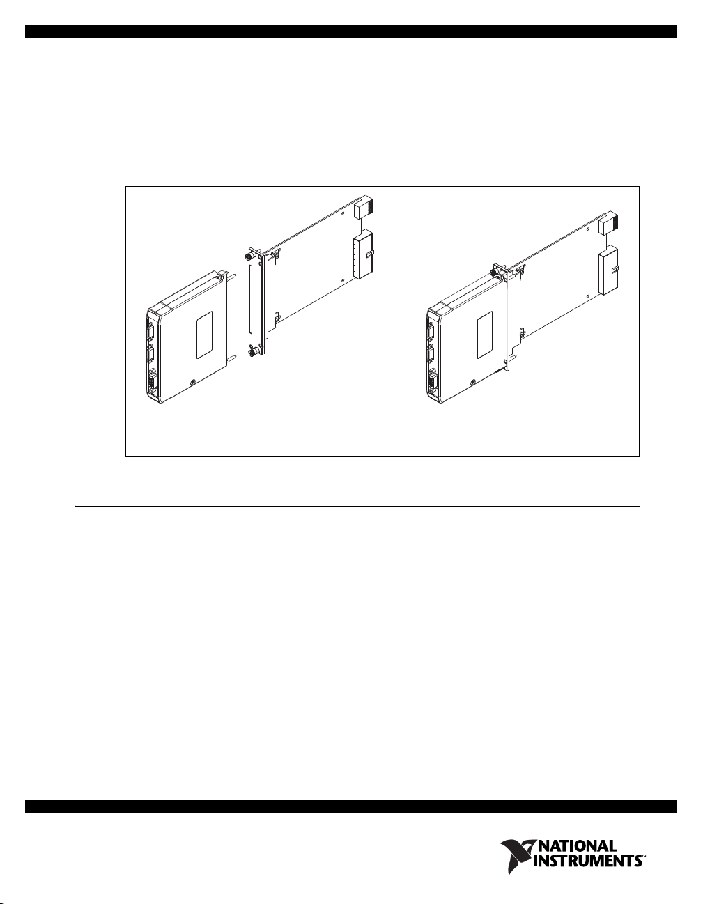
NI FlexRIO
FPGA Module
Figure 1. NI 1483R
NI 1483RNI 1483 + =
Page 2

❑ One of the following system considerations:
– PXI/CompactPCI or PXI Express/CompactPCI Express chassis with a PXI/CompactPCI or a
PXI Express/CompactPCI Express embedded controller
– MXI kit and a PC running Windows 7/Vista/XP/2000
❑ Cables for connecting a Camera Link-compatible camera to the NI 1483. Refer to the Connectivity
Options section for a list of applicable cables and accessories.
Step 1. Install Application Software and Driver
Before installing the NI 1483, you must install the application software and device driver. Install the
software in the following order:
1. LabVIEW—Refer to the LabVIEW Release Notes for installation instructions for LabVIEW
and system requirements for the LabVIEW software. Refer to the LabVIEW Upgrade Notes for
additional information about upgrading to the most recent version of LabVIEW for Windows.
Documentation for LabVIEW is available by selecting Start»All Programs»National
Instruments»LabVIEW»LabVIEW Manuals.
2. LabVIEW FPGA Module—Refer to the LabVIEW FPGA Module Release and Upgrade Notes
for installation instructions and information about getting started with the LabVIEW FPGA
Module.
Documentation for the LabVIEW FPGA Module is available by selecting Start»All Programs»
National Instruments»LabVIEW»LabVIEW Manuals.
3. NI-RIO—Refer to the NI-RIO Readme on the NI-RIO installation media for system requirements
and installation instructions for the NI-RIO driver.
Documentation for the NI-RIO driver software is available by selecting Start»All Programs»
National Instruments»NI-RIO.
4. NI-IMAQ—Refer to the NI Vision Acquisition Software Release Notes on the NI Vision
Acquisition Software installation media for system requirements and installation instructions for
the NI-IMAQ driver.
Documentation for the NI-IMAQ driver software is available by selecting Start»All Programs»
National Instruments»Vision»Documentation»NI-IMAQ.
5. (Optional) NI Vision Development Module—Refer to the NI Vision Development Module
Readme on the NI Vision Development Module installation media for system requirements and
installation instructions.
Documentation for the NI Vision Development Module is available by selecting Start»All
Programs»National Instruments»Vision»Documentation»NI Vision.
Step 2. Install the NI 1483
This section describes how to unpack and install the NI FlexRIO FPGA module and the NI 1483.
Note You must install the software before installing the hardware. For software installation
information, refer to Step 1. Install Application Software and Driver.
NI 1483R User Guide and Specifications 2 ni.com
Page 3

Unpacking
181716151312111098765432
NI PXIe-1065
3
1
H
14
HHH
2 234
51
The NI FlexRIO FPGA module and the NI 1483 are shipped in antistatic packages to prevent
electrostatic discharge from damaging device components. To prevent such damage when handling
the device, take the following precautions:
• Ground yourself using a grounding strap or by holding a grounded object, such as your computer
chassis.
• Touch the antistatic package to a metal part of the computer chassis before removing the device
from the package.
Caution Never touch the exposed pins of connectors.
Remove the device from the package and inspect the devices for loose components or any other sign
of damage. Notify National Instruments if the device appears damaged in any way. Do not install a
damaged device into the chassis.
Store the NI FlexRIO FPGA module and NI 1483 in the antistatic envelopes when not in use.
Installing the NI FlexRIO FPGA Module
Complete the following steps to install an NI FlexRIO FPGA module:
Note You must install the software before installing the hardware. For software installation
information, refer to Step 1. Install Application Software and Driver.
Caution Refer to the Read Me First: Safety and Electromagnetic Compatibility document packaged
with your PXI/PXI Express chassis or device before removing equipment covers or connecting or
disconnecting any signal wires.
1. Power off and unplug the PXI/PXI Express chassis. Refer to your chassis manual to install or
configure the chassis.
2. Identify a supported PXI/PXI Express slot in the chassis. Figure 2 shows the symbols that indicate
the slot types for a PXI/PXI Express chassis.
1 PXI Express System Controller Slot
2 PXI Peripheral Slots
3 PXI Express Hybrid Peripheral Slots
Figure 2. Symbols for PXI Express/PXI Express Hybrid/PXI Slots
© National Instruments Corporation 3 NI 1483R User Guide and Specifications
4 PXI Express Peripheral Slots
5 PXI Express System Timing Slot
Page 4
If you are using a PXI Express chassis, you can place PXI devices in the PXI slots. If a PXI device is
3
PXI-1000B
5
6
4
1
2
hybrid slot compatible, you can use the PXI Express Hybrid slots. PXI Express devices can be placed
only in PXI Express slots and PXI Express Hybrid slots. Refer to the chassis documentation for details.
Tip PXI NI FlexRIO FPGA modules are compatible with PXI slots and PXI Express Hybrid slots.
PXIe NI FlexRIO FPGA modules are compatible with PXI Express slots and PXI Express Hybrid
slots. National Instruments does not recommend using NI FlexRIO FPGA modules in PXI Express
System Timing slots because the boards do not have timing features.
3. Remove the filler panel of an unused PXI/PXI Express slot.
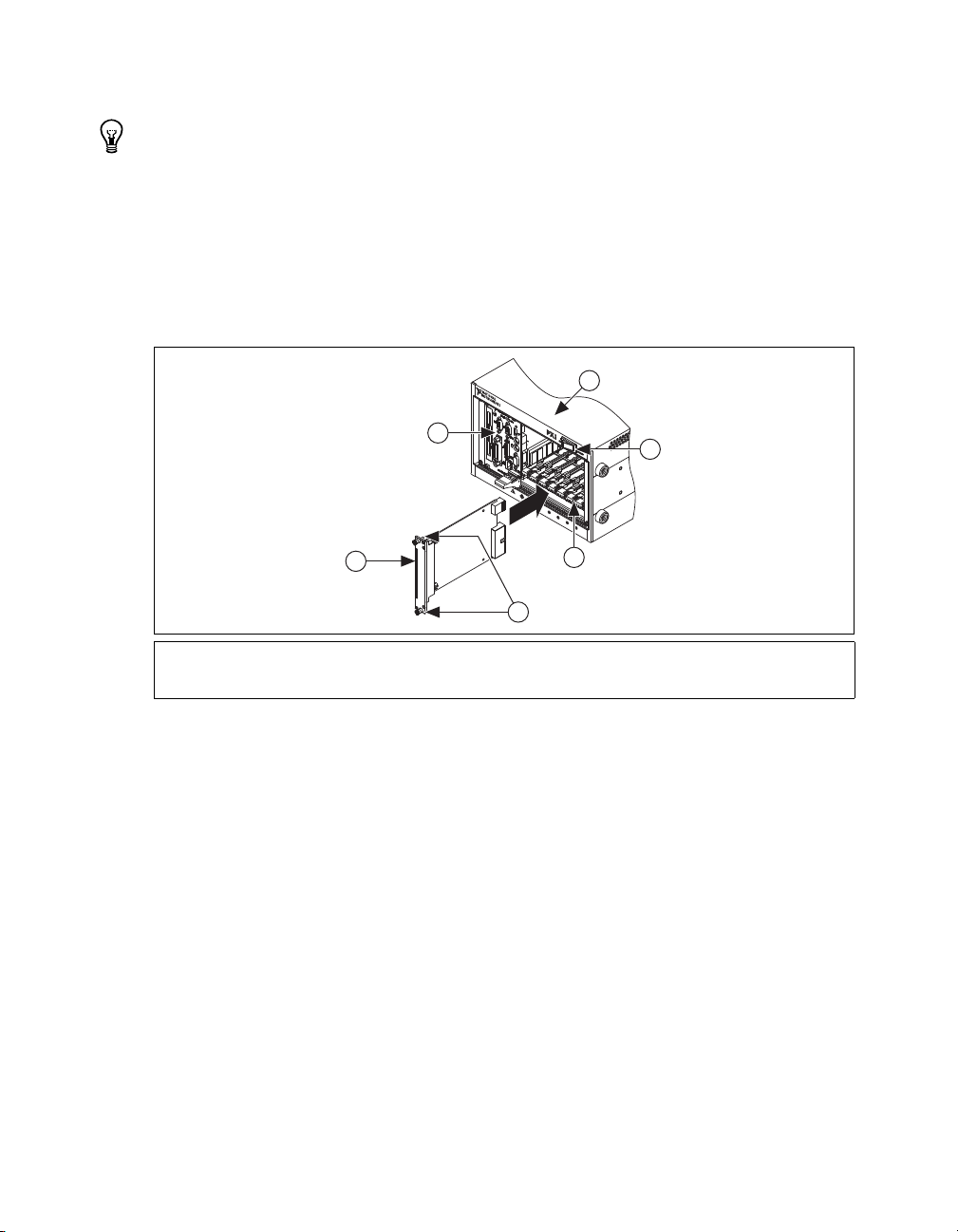
4. Touch any metal part of the chassis to discharge any static electricity.
5. Place the PXI/PXI Express module edges into the module guides at the top and bottom of the
chassis, and slide the module into the chassis until the module is fully inserted, as shown in
Figure 3.
1 PXI/PXI Express Chassis
2 PXI/PXI Express System Controller
3 NI FlexRIO FPGA Modu le
4 Front-Panel Mounting Screws
5Module Guides
6 Power Switch
Figure 3. Installing an NI FlexRIO FPGA Module in the PXI/PXI Express Chassis
6. Secure the device front panel to the chassis front panel mounting rail using the front-panel
mounting screws.
7. Plug in and power on the PXI/PXI Express chassis.
Confirming the Device is Recognized
To confirm that the device is recognized, complete the following additional steps:
1. Select Start»All Programs»National Instruments»Measurement & Automation to open
Measurement & Automation Explorer (MAX).
2. Expand Devices and Interfaces.
3. Verify that the device appears under Devices and Interfaces»RIO Devices.
Installing the NI 1483
Complete the following steps to connect the NI FlexRIO adapter module to the NI FlexRIO FPGA
NI 1483R User Guide and Specifications 4 ni.com
module.
1. Gently insert the guide pins and the high-density card edge of the NI 1483 into the corresponding
connectors of the NI FlexRIO FPGA module, as shown in Figure 4. The connection may be tight,
but do not force the adapter module into place.
Page 5
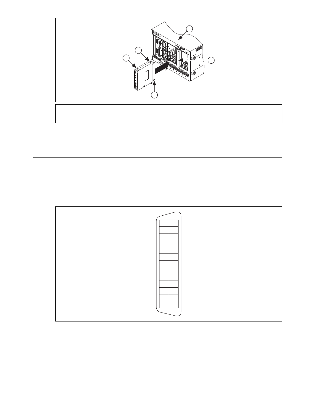
4
PXI-1000B
2
1
3
5
1 NI FlexRIO Adapter Module (NI 1483)
2Captive Screw
3 Guide Pin
2. Tighten the captive screws on the NI 1483 to secure it to the NI FlexRIO FPGA module.
Step 3. Connect Signals
This section describes the Base configuration 26-pin SDR connector, the Medium/Full configuration
26-pin SDR connector, and the 15-pin D-Sub connector on the NI 1483.
SDR Connectors
Figure 5 shows the NI 1483 Base configuration 26-pin SDR connector assignments. Refer to Table 1 for
a description of the signals.
4 PXI/PXI Express Chassis
5 NI FlexRIO FPGA Module
Figure 4. Installing the NI 1483
13
DGND
X(0)–
X(1)–
X(2)–
XCLK–
X(3)–
SerTC+
SerTFG–
CC(1)–
CC(2)+
CC(3)–
CC(4)+
DGND
26
25
24
23
22
21
20
19
18
17
16
15
14
12
11
10
9
8
7
6
5
4
3
2
1
DGND
X(0)+
X(1)+
X(2)+
XCLK+
X(3)+
SerTC–
SerTFG+
CC(1)+
CC(2)–
CC(3)+
CC(4)–
DGND
Figure 5. NI 1483 Base Configuration SDR Connector Pin Assignments
© National Instruments Corporation 5 NI 1483R User Guide and Specifications
Page 6
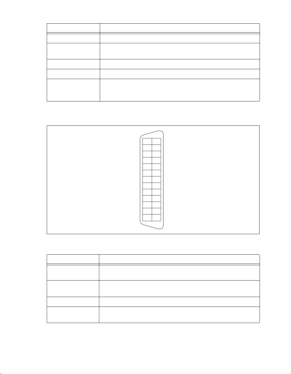
Table 1. NI 1483 Base Configuration SDR Signal Descriptions
DGND
Y(0)+
Y(1)+
Y(2)+
YCLK+
Y(3)+
100
Ω differential termination with pin 20
Z(0)+
Z(1)+
Z(2)+
ZCLK+
Z(3)+
DGND
DGND
Y(0)–
Y(1)–
Y(2)–
YCLK–
Y(3)–
100 Ω differential termination with pin 7
Z(0)–
Z(1)–
Z(2)–
ZCLK–
Z(3)–
DGND
13
12
11
10
9
8
7
6
5
4
3
2
1
26
25
24
23
22
21
20
19
18
17
16
15
14
Signal Name Description
X<3..0>± Base configuration data and enable signals from the camera to the NI 1483.
XCLK± Transmission clock on the Base configuration chip for Camera Link
communication between the NI 1483 and the camera.
SerTC± Serial transmission to the camera from the NI 1483.
SerTFG± Serial transmission to the NI 1483 from the camera.
CC<4..1>± Four LVDS pairs, defined as camera inputs and NI 1483 outputs, reserved
for camera control. On some cameras, the camera controls allow the
NI 1483 to control exposure time and frame rate.
Figure 6 shows the NI 1483 Medium/Full configuration 26-pin SDR connector assignments. Refer to
Table 2 for a description of the signals.
Figure 6. NI 1483 Medium/Full Configuration SDR Connector Pin Assignments
Signal Name Description
Y<3..0>± Medium configuration data and enable signals from the camera to the
YCLK± Transmission clock on the Medium configuration chip for Camera Link
Z<3..0>± Full configuration data and enable signals from the camera to the NI 1483.
ZCLK± Transmission clock on the Full configuration chip for Camera Link
NI 1483R User Guide and Specifications 6 ni.com
Table 2. NI 1483 Medium/Full Configuration SDR Signal Descriptions
NI 1483.
communication between the NI 1483 and the camera.
communication between the NI 1483 and the camera.
Page 7

D-Sub Connector
6
10
The 15-pin female high-density D-Sub connector connects to general purpose digital I/O, which
includes four TTL I/O lines, two optically isolated inputs, and two RS-422 quadrature encoder inputs.
Table 3 shows the connector assignments and descriptions.
Connector Pin Signal Name Description
15
11
Table 3. NI 1483 15-pin D-Sub Connector Pin Assignments
1 TTL I/O 0 TTL external trigger/Digital I/O line.
2 Iso Input 0+ 30 V isolated input only line.
3 Phase A+ Quadrature encoder Phase A positive
connection for single-ended or differential
signals. Can also be used as a digital input for
triggering.
4 Phase B– Quadrature encoder Phase B negative
connection for differential signals.
5 NC No connection.
5
6 TTL I/O 1 TTL external trigger/Digital I/O line.
7 TTL I/O 2 TTL external trigger/Digital I/O line.
8 Iso Input 1+ 30 V isolated input only line.
9 Phase B+ Quadrature encoder Phase B positive
connection for single-ended or differential
signals. Can also be used as a digital input for
triggering.
1
10 TTL I/O 3 TTL external trigger/Digital I/O line.
11 Digital Ground Direct connection to digital ground on the
NI 1483.
12 Iso Input 0–
Isolated reference.
Iso Input 1–
13 Phase A– Quadrature encoder Phase A negative
connection for differential signals.
14 Digital Ground Direct connection to digital ground on the
NI 1483.
15 NC No connection.
© National Instruments Corporation 7 NI 1483R User Guide and Specifications
Page 8

Connectivity Options
National Instruments recommends that you use the following cables to connect your camera to the
26-pin SDR connectors on the NI 1483:
• MDR to SDR Camera Link cable (part number 199745A-05)
• SDR to SDR Camera Link cable (part number 199746A-05)
Note To ensure the high-speed signaling of the Camera Link interface, National Instruments
recommends that you purchase a Camera Link cable rather than build a custom cable.
You can use the NI 1483 with the following I/O accessories:
• NI 17xx 5m Pigtail breakout cable (part number 197818-05)
• NI 17xx Unshielded Screw Terminal Breakout with 2M Cable (part number 780261-01)
Step 4. Using the NI 1483R with a LabVIEW FPGA Example VI
This section demonstrates how to use an existing LabVIEW FPGA example project to acquire images
with the NI 1483R.
Note Examples available for your device are dependent on the device-specific minimum software
requirements. For more information about software requirements for your device, refer to Step 1.
Install Application Software and Driver.
Each NI 1483R example project includes:
• A LabVIEW FPGA VI that can be compiled and run on FPGA hardware
• A Host VI that runs in LabVIEW for Windows and interacts with the LabVIEW FPGA VI
Note In software, NI FlexRIO adapter modules are referred to as IO Modules.
Complete the following steps to run an example that acquires an image with the NI 1483.
1. Connect a Camera Link camera capable of outputting a 1-tap, 10-bit image to the NI 1483. Ensure
that the camera is powered on.
2. This example shows how to use a frame trigger to acquire images from the camera. To use an
external trigger source, connect the TTL I/O 0 pin on the D-Sub connector to the trigger source
using either a breakout cable or terminal block. If you do not have an external trigger source, you
can trigger the camera with a software trigger.
3. Launch LabVIEW.
4. In the Getting Started window, click Find Examples to display the NI Example Finder.
5. In the NI Example Finder window, select Directory Structure.
6. Browse to the example folder for the NI 1483 by selecting FlexRIO»IO Modules»NI 1483.
7. Select 1-Tap 10-Bit Camera with Frame Trigger, then 1-Tap 10-Bit Camera with Frame
Trigger.lvproj.
8. In the Project Explorer window, expand the tree view for the FPGA target you are using. If your
target does not appear, complete the following steps to create and configure a new FPGA target.
a. In the Project Explorer window, right-click My Computer and select New»Targets and
Devices.
b. Select the type of FPGA target you intend to use and click OK.
c. Expand the tree view for the PXIe-7965R and the tree view for the target you created.
NI 1483R User Guide and Specifications 8 ni.com
Page 9

d. Hold down the Ctrl key and click the 100 MHz Clock, Host DMA 16, and 1-Tap 10-Bit
Camera with Frame Trigger (FPGA).vi.
e. Select Edit»Copy from the menu bar.
f. Select the new FPGA target you created.
g. Select Edit»Paste from the menu bar.
h. Right-click on IO Module (None) under the FPGA target you created and select Properties.
i. Enable the Enable IO Module checkbox.
j. Select the NI 1483 under the list of IO Modules.
k. Click Clock Selections in the Category list.
l. Select 40 MHz Onboard Clock for Clock 40 MHz and select 100 MHz Clock for the Image
Data Clock.
m. Click OK.
n. Right click on 1-Tap 10-Bit Camera with Frame Trigger (FPGA).vi and select Create Build
Specification.
9. Expand the Build Specifications tree view. Right-click 1-Tap 10-Bit Camera with Frame
Trigger (FPGA), and, select Build from the drop-down menu.
Note Depending on your hardware configuration, compiling may take 30 minutes to an hour.
10. In the Project Explorer window, double-click 1-Tap 10-Bit Camera with Frame Trigger
(Host).vi under My Computer to open the host VI. The VI uses the NI PXIe-7965R as the FPGA
target. If you are not using the NI PXIe-7965R, complete the following steps to change the FPGA
target.
a. In the host VI front panel window, select Window»Show Block Diagram to open the VI
block diagram.
b. On the block diagram, right-click the Open FPGA icon (PXIe-7965R) and select Configure
Open FPGA VI Reference.
c. In the Configure Open FPGA VI Reference window, click the Browse Project button in the
Open VI section.
d. In the Select VI window that opens, expand the tree view for your device, select the VI under
your device and click OK.
e. Click OK in the Configure Open FPGA VI Reference window.
f. Save the VI.
11. On the front panel, select your FlexRIO device from the RIO Device drop-down listbox.
12. In the Image Width and Image Height spin boxes, enter the values that match the camera output.
13. The value of the Trigger Pulse Width (us) spin box will control the pulse width of the frame
trigger that is sent to the camera on Camera Link control line 1. Set this value to satisfy the pulse
width requirements of the camera in use.
14. Set the Start Serial Server button to true to enable the serial server. The button illuminates when
true. You can use the serial server to communicate with the camera, and configure the camera using
the configuration utility provided by the camera manufacturer.
15. On the front panel of the 1-Tap 10-Bit Camera with Frame Trigger (Host).vi, click the Run
button to run the VI. Check if the Module Enabled and Initalized status indicators are lit. If
Module Enabled is not lit, verify the NI 1483 adapter module is properly connected to the
NI FlexRIO FPGA module. If Initalized is not lit, verify the camera is properly connected and
powered on.
© National Instruments Corporation 9 NI 1483R User Guide and Specifications
Page 10

16. If the camera is not configured for triggering using Camera Link control line 1, configure it using
the camera manufacturer’s configuration utility. Verify the camera width and height configuration
matches the values entered in the Image Width and Image Height spin boxes. The host VI must be
running for the manufacturer’s configuration utility to be able to communicate with the camera.
17. Once the camera is configured, click the Acquire button on the VI front panel. Clicking Acquire
initiates a single-frame acquisition. If the camera is properly configured, it will not output a frame
until a trigger is provided. Supply a trigger by sending a pulse on TTL I/O 0 or by clicking the
SW Trigger button. Repeat this step to acquire another image.
18. Click the STOP button to stop the VI.
19. Close the VI.
Step 5. Modifying the LabVIEW FPGA Example VI to Add a Threshold
This section demonstrates how to modify the NI 1483 example VI to add thresholding.
1. Launch LabVIEW. If LabVIEW is already running, select Help»Find Examples.
2. In the Getting Started window, click Find Examples to display the NI Example Finder.
3. In the NI Example Finder window, select Directory Structure.
4. Browse to the example folder for the NI 1483 by selecting FlexRIO»IO Modules»NI 1483.
5. Select 1-Tap 10-Bit Camera with Frame Trigger, then 1-Tap 10-Bit Camera with Frame
Trigger.lvproj.
6. In the Project Explorer window, right-click Project: 1-Tap 10-Bit Camera with Frame
Trigger.lvproj and select Explore.
7. In Windows Explorer, navigate up one folder to the NI 1483 folder. Copy the 1-Tap 10-Bit
Camera with Frame Trigger folder and rename the copy to 1-Tap 10-Bit Camera with
Frame Trigger and Threshold.
8. Close the LabVIEW Project Explorer window.
9. In Windows Explorer, navigate to the 1-Tap 10-Bit Camera with Frame Trigger and Threshold
folder, and double-click 1-Tap 10-Bit Camera with Frame Trigger.lvproj.
10. In the Project Explorer window, right-click Project: 1-Tap 10-Bit Camera with Frame
Trigger.lvproj and select Rename. Rename the project to 1-Tap 10-Bit Camera with Frame
Trigger and Threshold.lvproj.
11. Rename the 1-Tap 10-Bit Camera with Frame Trigger (Host).vi to 1-Tap 10-Bit Camera with
Frame Trigger and Threshold (Host).vi.
12. Expand the FPGA target for your device and rename the 1-Tap 10-Bit Camera with Frame
Trigger (FPGA).vi to 1-Tap 10-Bit Camera with Frame Trigger and Threshold (FPGA).vi.
13. Right-click the FPGA target for your device and select New»FIFO.
14. In the FIFO Properties window, configure the parameters as follows:
• Set the Name to Pixel Data 16
• Set the Type to Target-Scoped
• Set the Requested Number of Elements to 1023
• Set the Implementation to Block Memory
• Set the Data Type to U16.
15. Click OK.
16. Under the FPGA target for your device, double-click 1-Tap 10-Bit Camera with Frame Trigger
and Threshold (FPGA).vi.
NI 1483R User Guide and Specifications 10 ni.com
Page 11

17. In the VI front panel, select Window»Show Block Diagram.
18. In the Acquisition loop, locate the Host DMA 16 FIFO. Right-click the Host DMA 16 FIFO and
select Select FIFO»Pixel Data 16.
19. Expand the sequence structure downward.
20. Below the Camera Trigger loop, add a new Timed Loop to the block diagram by selecting it from
the Programming»Structures»Timed Structures»Timed Loop palette.
21. Right-click the clock icon on the left side of the Timed Loop and select Configure Input Node.
22. In the Configure Timed Loop window, configure the loop as shown in Figure 7.
Figure 7. Configuring the Timed Loop Properties
23. Refer to Figure 8 while completing the following steps to build the threshold loop.
Figure 8. Threshold Loop
a. Add 4 FIFO Method Nodes from the Programming»Memory & FIFO palette to the
Threshold loop.
b. Configure two of the FIFO Method Nodes to be Pixel Data 16 nodes by right-clicking the
nodes and selecting Select FIFO»Pixel Data 16.
c. Right-click one of the Pixel Data 16 nodes, and select Select Method»Status»Get Number
of Elements to Read.
d. Right-click the other Pixel Data 16 node, and select Select Method»Read.
© National Instruments Corporation 11 NI 1483R User Guide and Specifications
Page 12

e. Configure the two unconfigured FIFO Method Nodes to be Host DMA 16 nodes by
right-clicking the nodes and selecting Select FIFO»Host DMA 16.
f. Right-click one of the Host DMA 16 nodes, and select Select Method»Status»Get Number
of Elements to Write.
g. Right-click the other Host DMA 16 node, and select Select Method»Write.
h. Complete the threshold loop by wiring the block diagram as shown in Figure 8. The
U16 control names are Threshold.Upper Limit, Threshold.Lower Limit, and
Threshold.Replacement Value. The Boolean control name is Threshold.Replace Value?.
i. Save the VI.
24. In the Project Explorer window, expand the Build Specifications tree view under the target you are
using. Right-click 1-Tap 10-Bit Camera with Frame Trigger and select Build.
25. Save the project after the compilation completes.
26. In the Project Explorer window, double-click 1-Tap 10-Bit Camera with Frame Trigger and
Threshold (Host).vi. Complete the following steps to update the FPGA target.
j. In the host VI front panel window, select Window»Show Block Diagram to open the
VI block diagram.
k. On the block diagram, right-click the Open FPGA icon (PXIe-7965R) and select Configure
Open FPGA VI Reference.
l. In the Configure Open FPGA VI Reference window, click the Browse Project button in the
Open VI section.
m. In the Select VI window that opens, expand the tree view for your device, select the VI under
your device and click OK.
n. Click OK in the Configure Open FPGA VI Reference window.
o. Save the VI.
27. On the block diagram, locate the loop labeled Update configuration settings and monitor the
acquisition status. While referring to Figure 9, add the following elements to the Read/Write
control in the loop: Threshold.Upper Limit, Threshold.Lower Limit, Threshold.Replace
Value?, and Threshold.Replacement Value. Create controls for each new element.
Figure 9. Send Software Triggers Loop
28. Save the VI.
29. Run the VI as before, adjusting the threshold controls to achieve the desired results.
NI 1483R User Guide and Specifications 12 ni.com
Page 13

NI 1483 Component-Level Intellectual Property (CLIP)
Adapter Module
CLIP Socket
LabVIEW
FPGA VI
User-Defined
CLIP
NI FlexRIO FPGA Module
FPGA
External
I/O Connector
Adapter
Module
User-Defined
CLIP
Fixed I/O
Socketed
CLIP
DRAM 1
CLIP Socket
DRAM 0
CLIP Socket
Socketed
CLIP
Socketed
CLIP
Fixed I/O
DRAM0 DRAM1
Fixed I/O
The LabVIEW FPGA Module includes a feature for HDL IP integration called CLIP. NI FlexRIO
devices support two types of CLIP: user-defined and socketed.
• A user-defined CLIP allows you to insert HDL IP into an FPGA target, enabling VHDL code to
communicate directly with an FPGA VI.
• NI FlexRIO devices also support socketed CLIP, which provides the same IP integration
functionality of the user-defined CLIP, while also allowing the CLIP to communicate directly with
circuitry external to the FPGA. Adapter module socketed CLIP allows your IP to communicate
directly with both the FPGA VI and the external adapter module connector interface.
Figure 10 shows the relationship between an FPGA VI and the CLIP.
Figure 10. CLIP Relationship
The NI 1483 ships with socketed CLIP that is used to add module I/O to the LabVIEW project.
The NI-developed NI 1483 CLIP supports Base, Medium, Full, and 80-bit Camera Link configurations.
Camera Link data outputs on ten 8-bit Camera Link ports (A through J) along with flags, all of which
are synchronous to the user-selected Image Data Clock. The CLIP also provides access to the Camera
Link serial interface, four camera control lines, four TTL I/O lines, two isolated inputs, and inputs for a
quadrature encoder.
© National Instruments Corporation 13 NI 1483R User Guide and Specifications
Refer to the NI FlexRIO Adapter Module Support Help topic of the LabVIEW Help for information
regarding NI FlexRIO CLIP, configuring the NI 1483 with a socketed CLIP, and a list of available
socketed CLIP and provided signals.
Page 14

Specifications
This section lists the specifications of the NI 1483. Pair these specifications with the NI FlexRIO FPGA
Module Specifications. These specifications are typical at 25 °C, unless otherwise stated.
Features
Supported camera standard....................................Camera Link 1.2
Supported configurations.......................................Base, Medium, Full, 80-bit/10-tap
Camera connectors.................................................Two 26-pin SDR
General-purpose digital I/O connectors.................One 15-pin high-density female D-Sub
Trigger Characteristics
Number of external trigger I/O lines......................4
Trigger input
Voltage range .................................................0 to 5 V (TTL)
Input high voltage ..................................2.0 V
Input low voltage ...................................0.8 V
Polarity...........................................................Programmable, active high or active low
Trigger output
Voltage range .................................................0 to 5 V (TTL)
Output high voltage................................3.06 V at 3 mA source
Output low voltage.................................0.55 V at 3 mA sink
Polarity...........................................................Programmable, active high or active low
Maximum pulse rate ..............................................2 MHz
Input Characteristics
Optically Isolated Inputs
Number of channels ...............................................2
Type........................................................................Current sinking
Input voltage range ................................................0 to 30 V
Input ON voltage............................................3.5 to 30 V
Input OFF voltage ..........................................0 to 2 V
Turn-on current ......................................................7.1 mA (typical)
14 mA (maximum)
Maximum pulse rate ..............................................100 kHz
Minimum pulse detected........................................10 μs
Reverse polarity protection .................................... Yes, –30 V
NI 1483R User Guide and Specifications 14 ni.com
Page 15

Quadrature Encoder/RS-422 Inputs
Number of channels ...............................................2
Input type ...............................................................Differential or single-ended
Voltage range .........................................................0 to 5.5 VDC
Logic levels
Differential input threshold............................±0.2 V (maximum),
RS-422 compatible
Single-ended input threshold .........................TTL compatible
Input high voltage ..................................2.0 V
Input low voltage ...................................0.8 V
Maximum quadrature count rate............................5 MHz
Clocks
Pixel clock frequency range...................................20 MHz to 85 MHz
Note The Camera Link specification requires cameras to transmit at a minimum of 20 MHz.
Serial Interface
Baud rates supported..............................................9.6, 19.2, 38.4, 57.6, 115.2, 230.4, 460.8,
Power Requirements
Voltage ...................................................................+3.3 V (300 mA)
Physical Characteristics
Dimensions
Connectors to back of module .......................12.2 cm (4.8 in.)
Mounting screw to mounting screw...............12.8 cm (5.0 in.)
Width..............................................................2.0 cm (0.8 in.)
Weight ....................................................................293 g (10.3 oz)
Environment
The NI 1483 is intended for indoor use only.
Operating Environment
Operating temperature ...........................................0 °C to 55 °C,
Relative humidity range.........................................10% to 90%, noncondensing,
1
or 921.6 kbps
+12 V (50 mA)
Tested in accordance with IEC-60068-2-1
and IEC-60068-2-2
Tested in accordance with IEC-60068-2-56
Altitude ..................................................................2,000 m at 25 °C ambient temperature
Pollution Degree ....................................................2
1
This value corresponds to the serialized Camera Link cable transmission rate of 140 to 595 MHz.
© National Instruments Corporation 15 NI 1483R User Guide and Specifications
Page 16

Storage Environment
Ambient temperature range ...................................–20 °C to 70 °C
Relative humidity range.........................................5% to 95%, noncondensing,
Note Clean the device with a soft, non-metallic brush. Make sure the device is completely dry and
free from contaminants before returning it to service.
Shock and Vibration
Operational shock ..................................................30 g peak, half-sine, 11 ms pulse
Random vibration
Operating .......................................................5 to 500 Hz, 0.3 grms
Nonoperating .................................................5 to 500 Hz, 2.4 grms
Safety
This product meets the requirements of the following standards of safety for electrical equipment for
measurement, control, and laboratory use:
• IEC 61010-1, EN 61010-1
• UL 61010-1, CSA 61010-1
Note For UL and other safety certifications, refer to the product label or the Online Product
Certification section.
Tested in accordance with IEC-60068-2-1
and IEC-60068-2-2
Tested in accordance with IEC-60068-2-56
Tested in accordance with IEC-60068-2-27.
Test profile developed in accordance with
MIL-PRF-28800F.
Tested in accordance with IEC-60068-2-64.
Nonoperating test profile exceeds the requirements
of MIL-PRF-28800F, Class 3.
Electromagnetic Compatibility
This product meets the requirements of the following EMC standards for electrical equipment for
measurement, control, and laboratory use:
• EN 61326 (IEC 61326): Class A emissions; Basic immunity
• EN 55011 (CISPR 11): Group 1, Class A emissions
• AS/NZS CISPR 11: Group 1, Class A emissions
• FCC 47 CFR Part 15B: Class A emissions
• ICES-001: Class A emissions
Note For the standards applied to assess the EMC of this product, refer to the Online Product
Certification section.
Note For EMC compliance, operate this device with shielded cables and according to the
documentation.
NI 1483R User Guide and Specifications 16 ni.com
Page 17

CE Compliance
⬉ᄤֵᙃѻક∵ᶧࠊㅵ⧚ࡲ⊩ ˄Ё
RoHS
˅
Ёᅶ᠋
National Instruments
ヺড়Ё⬉ᄤֵᙃѻકЁ䰤ࠊՓ⫼ᶤѯ᳝ᆇ⠽䋼ᣛҸ
(RoHS)
DŽ
݇Ѣ
National Instruments
Ё
RoHS
ড়㾘ᗻֵᙃˈ䇋ⱏᔩ
ni.com/environment/rohs_china
DŽ
(For information about China RoHS compliance, go to
ni.com/environment/rohs_china
.)
This product meets the essential requirements of applicable European Directives as follows:
• 2006/95/EC; Low-Voltage Directive (safety)
• 2004/108/EC; Electromagnetic Compatibility Directive (EMC)
Online Product Certification
Refer to the product Declaration of Conformity (DoC) for additional regulatory compliance
information. To obtain product certifications and the DoC for this product, visit
certification
Certification column.
, search by model number or product line, and click the appropriate link in the
Environmental Management
NI is committed to designing and manufacturing products in an environmentally responsible manner.
NI recognizes that eliminating certain hazardous substances from our products is beneficial to the
environment and to NI customers.
For additional environmental information, refer to the NI and the Environment Web page at ni.com/
environment
complies, as well as other environmental information not included in this document.
Waste Electrical and Electronic Equipment (WEEE)
EU Customers At the end of the product life cycle, all products must be sent to a WEEE recycling
center. For more information about WEEE recycling centers, National Instruments WEEE initiatives,
and compliance with WEEE Directive 2002/96/EC on Waste and Electronic Equipment,
visit
. This page contains the environmental regulations and directives with which NI
ni.com/environment/weee.
ni.com/
Where to Go From Here
The following resources contain information for writing applications and acquiring images with the
NI 1483R.
Software Documentation
• LabVIEW FPGA documentation:
– FPGA Module book in the LabVIEW Help—Select Help»Search the LabVIEW Help in
LabVIEW to view the LabVIEW Help. Browse the FPGA Module book in the Contents tab
for information about how to use the FPGA Module to create VIs that run on the NI 1483.
– LabVIEW FPGA Module Release and Upgrade Notes—Contains information about installing
the LabVIEW FPGA Module, describes new features, and provides upgrade information.
To access this document, refer to
Manuals directory that contains this document by selecting Start»All Programs»National
Instruments»LabVIEW»LabVIEW Manuals.
• National Instruments Example Finder—LabVIEW contains an extensive library of VIs and
example programs for use with NI FlexRIO devices. To access the NI Example Finder, open
LabVIEW and select Help»Find Examples, then select Hardware Input and Output»FlexRIO.
© National Instruments Corporation 17 NI 1483R User Guide and Specifications
ni.com/manuals. You can also view the LabVIEW
Page 18

You can also access device-specific examples by selecting Add device from the Hardware
pull-down menu in the NI Example Finder window.
• NI FlexRIO Reference and Procedures book in the LabVIEW Help—Select Help»Search the
LabVIEW Help in LabVIEW to view the LabVIEW Help. Browse the FPGA Module book in
the Contents tab for instructions for using LabVIEW and the LabVIEW FPGA Module with
NI FlexRIO devices.
Additional Resources
• NI FlexRIO FPGA Module Specifications—Lists the specifications of your NI FlexRIO FPGA
module. To access these documents, refer to
• LabVIEW FPGA IPNet—Offers resources for browsing, understanding, and downloading
LabVIEW FPGA functions or IP (intellectual property). Use this resource to acquire IP that you
need for your application, download examples to help learn programming techniques, and explore
the depth of IP offered by the LabVIEW FPGA platform. To access the LabVIEW FPGA IPNet,
visit ni.com/ipnet.
• ni.com/flexrio—Contains product information, and helpful links to the NI FlexRIO forum
and the NI community for NI FlexRIO devices.
Where to Go for Support
The National Instruments Web site is your complete resource for technical support. At ni.com/
support
resources to email and phone assistance from NI Application Engineers.
National Instruments corporate headquarters is located at 11500 North Mopac Expressway, Austin,
Texas, 78759-3504. National Instruments also has offices located around the world to help address your
support needs. For telephone support in the United States, create your service request at
support
United States, visit the Worldwide Offices section of ni.com/niglobal to access the branch office
Web sites, which provide up-to-date contact information, support phone numbers, email addresses, and
current events.
you have access to everything from troubleshooting and application development self-help
and follow the calling instructions or dial 512 795 8248. For telephone support outside the
ni.com/manuals.
ni.com/
NI 1483R User Guide and Specifications 18 ni.com
Page 19

LabVIEW, National Instruments, NI, ni.com, the National Instruments corporate logo, and the Eagle
logo are trademarks of National Instruments Corporation. Refer to the Trademark Information at
ni.com/trademarks for other National Instruments trademarks. Other product and company
names mentioned herein are trademarks or trade names of their respective companies. For patents
covering National Instruments products/technology, refer to the appropriate location: Help»Patents
in your software, the patents.txt file on your media, or the National Instruments Patent Notice
at ni.com/patents. Refer to the Export Compliance Information at ni.com/legal/
export-compliance for the National Instruments global trade compliance policy and how to
obtain relevant HTS codes, ECCNs, and other import/export data.
© 2010–2011 National Instruments Corporation. All rights reserved.
375502B-01 Sep11
 Loading...