

Page 1

TM
SCXI
SCXI-1141/1142/1143 User Manual
SCXI-1141/1142/1143 User Manual
May 2007
371748E-01
Page 2

Support
Worldwide Technical Support and Product Information
ni.com
National Instruments Corporate Headquarters
11500 North Mopac Expressway Austin, Texas 78759-3504 USA Tel: 512 683 0100
Worldwide Offices
Australia 1800 300 800, Austria 43 662 457990-0, Belgium 32 (0) 2 757 0020, Brazil 55 11 3262 3599,
Canada 800 433 3488, China 86 21 5050 9800, Czech Republic 420 224 235 774, Denmark 45 45 76 26 00,
Finland 385 (0) 9 725 72511, France 33 (0) 1 48 14 24 24, Germany 49 89 7413130, India 91 80 41190000,
Israel 972 3 6393737, Italy 39 02 413091, Japan 81 3 5472 2970, Korea 82 02 3451 3400,
Lebanon 961 (0) 1 33 28 28, Malaysia 1800 887710, Mexico 01 800 010 0793, Netherlands 31 (0) 348 433 466,
New Zealand 0800 553 322, Norway 47 (0) 66 90 76 60, Poland 48 22 3390150, Portugal 351 210 311 210,
Russia 7 495 783 6851, Singapore 1800 226 5886, Slovenia 386 3 425 42 00, South Africa 27 0 11 805 8197,
Spain 34 91 640 0085, Sweden 46 (0) 8 587 895 00, Switzerland 41 56 2005151, Taiwan 886 02 2377 2222,
Thailand 662 278 6777, Turkey 90 212 279 3031, United Kingdom 44 (0) 1635 523545
For further support information, refer to the Technical Support Information document. To comment on National
Instruments documentation, refer to the National Instruments Web site at
feedback.
ni.com/info and enter the info code
© 1994–2007 National Instruments Corporation. All rights reserved.
Page 3

Important Information
Warranty
The SCXI-1141, SCXI-1142, and SCXI-1143 modules are warranted against defects in materials and workmanship for a period of one year
from the date of shipment, as evidenced by receipts or other documentation. National Instruments will, at its option, repair or replace equipment
that proves to be defective during the warranty period. This warranty includes parts and labor.
The media on which you receive National Instruments software are warranted not to fail to execute programming instructions, due to defects in
materials and workmanship, for a period of 90 days from date of shipment, as evidenced by receipts or other documentation. National Instruments
will, at its option, repair or replace software media that do not execute programming instruc tions if National Instruments receives notice of such defects
during the warranty period. National Instruments does not warrant that the operation of the software shall be uninterrupted or error free.
A Return Material Authorization (RMA) number must be obtained from the factory and clearly marked on the outside of the package before any
equipment will be accepted for warranty work. National Instruments will pay the shipping costs of returning to the owner parts which are covered by
warranty.
National Instruments believes that the information in this document is accurate. The document has been carefully reviewed for technical accuracy. In
the event that technical or typographical errors exist, National Instruments reserves the right to make changes to subsequent editions of this document
without prior notice to holders of this edition. The reader should consult National Instruments if errors are suspected. In no event shall National
Instruments be liable for any damages arising out of or related to this document or the information contained in it.
E
XCEPT AS SPECIFIED HEREIN, NATIONAL INSTRUMENTS MAKES NO WARRANTIES, EXPRESS OR IMPLIED, AND SPECIFICALLY DISCLAIMS ANY WARRANTY OF
MERCHANTABILITY OR FITNESS FOR A PARTICULAR PURPOSE. CUSTOMER’S RIGHT TO RECOVER DAMAGES CAUSED BY FAULT OR NEGLIGENCE ON THE PART OF NATIONAL
I
NSTRUMENTS SHALL BE LIMITED TO THE AMOUNT THERETOFORE PAID BY THE CUSTOMER. NATIONAL INSTRUMENTS WILL NOT BE LIABLE FOR DAMAGES RESULTING
FROM LOSS OF DATA, PROFITS, USE OF PRODUCTS, OR INCIDENTAL OR CONSEQUENTIAL DAMAGES, EVEN IF ADVISED OF THE POSSIBILITY THEREOF. This limitation of
the liability of National Instruments will apply regardless of the form of action, whether in contract or tort, including negligence. Any action against
National Instruments must be brought within one year after the cause of action accrues. National Instruments shall not be liable for any delay in
performance due to causes beyond its reasonable control. The warranty provided herein does not cover damages, defects, malfunctions, or service
failures caused by owner’s failure to follow the National Instruments installation, operation, or maintenance instructions; owner’s modification of the
product; owner’s abuse, misuse, or negligent acts; and power failure or surges, fire, flood, accident, actions of third parties, or other events outside
reasonable control.
Copyright
Under the copyright laws, this publication may not be reproduced or transmitted in any form, electronic or mechanical, including photocopying,
recording, storing in an information retrieval system, or translating, in whole or in part, without the prior written consent of National
Instruments Corporation.
National Instruments respects the intellectual property of others, and we ask our users to do the same. NI software is protected by copyright and other
intellectual property laws. Where NI software may be used to reproduce software or other materials belonging to others, you may use NI software only
to reproduce materials that you may reproduce in accordance with the terms of any applicable license or other legal restriction.
Trademarks
National Instruments, NI, ni.com, and LabVIEW are trademarks of National Instruments Corporation. Refer to the Terms of Use section
on
ni.com/legal for more information about National Instruments trademarks.
Other product and company names mentioned herein are trademarks or trade names of their respective companies.
Patents
For patents covering National Instruments products, refer to the appropriate location: Help»Patents in your software, the patents.txt file
on your CD, or
ni.com/patents.
WARNING REGARDING USE OF NATIONAL INSTRUMENTS PRODUCTS
(1) NATIONAL INSTRUMENTS PRODUCTS ARE NOT DESIGNED WITH COMPONENTS AND TESTING FOR A LEVEL OF
RELIABILITY SUITABLE FOR USE IN OR IN CONNECTION WITH SURGICAL IMPLANTS OR AS CRITICAL COMPONENTS IN
ANY LIFE SUPPORT SYSTEMS WHOSE FAILURE TO PERFORM CAN REASONABLY BE EXPECTED TO CAUSE SIGNIFICANT
INJURY TO A HUMAN.
(2) IN ANY APPLICATION, INCLUDING THE ABOVE, RELIABILITY OF OPERATION OF THE SOFTWARE PRODUCTS CAN BE
IMPAIRED BY ADVERSE FACTORS, INCLUDING BUT NOT LIMITED TO FLUCTUATIONS IN ELECTRICAL POWER SUPPLY,
COMPUTER HARDWARE MALFUNCTIONS, COMPUTER OPERATING SYSTEM SOFTWARE FITNESS, FITNESS OF COMPILERS
AND DEVELOPMENT SOFTWARE USED TO DEVELOP AN APPLICATION, INSTALLATION ERRORS, SOFTWARE AND HARDWARE
COMPATIBILITY PROBLEMS, MALFUNCTIONS OR FAILURES OF ELECTRONIC MONITORING OR CONTROL DEVICES,
TRANSIENT FAILURES OF ELECTRONIC SYSTEMS (HARDWARE AND/OR SOFTWARE), UNANTICIPATED USES OR MISUSES, OR
ERRORS ON THE PART OF THE USER OR APPLICATIONS DESIGNER (ADVERSE FACTORS SUCH AS THESE ARE HEREAFTER
COLLECTIVELY TERMED “SYSTEM FAILURES”). ANY APPLICATION WHERE A SYSTEM FAILURE WOULD CREATE A RISK OF
HARM TO PROPERTY OR PERSONS (INCLUDING THE RISK OF BODILY INJURY AND DEATH) SHOULD NOT BE RELIANT SOLELY
UPON ONE FORM OF ELECTRONIC SYSTEM DUE TO THE RISK OF SYSTEM FAILURE. TO AVOID DAMAGE, INJURY, OR DEATH,
THE USER OR APPLICATION DESIGNER MUST TAKE REASONABLY PRUDENT STEPS TO PROTECT AGAINST SYSTEM FAILURES,
INCLUDING BUT NOT LIMITED TO BACK-UP OR SHUT DOWN MECHANISMS. BECAUSE EACH END-USER SYSTEM IS
CUSTOMIZED AND DIFFERS FROM NATIONAL INSTRUMENTS' TESTING PLATFORMS AND BECAUSE A USER OR APPLICATION
DESIGNER MAY USE NATIONAL INSTRUMENTS PRODUCTS IN COMBINATION WITH OTHER PRODUCTS IN A MANNER NOT
EVALUATED OR CONTEMPLATED BY NATIONAL INSTRUMENTS, THE USER OR APPLICATION DESIGNER IS ULTIMATELY
RESPONSIBLE FOR VERIFYING AND VALIDATING THE SUITABILITY OF NATIONAL INSTRUMENTS PRODUCTS WHENEVER
NATIONAL INSTRUMENTS PRODUCTS ARE INCORPORATED IN A SYSTEM OR APPLICATION, INCLUDING, WITHOUT
LIMITATION, THE APPROPRIATE DESIGN, PROCESS AND SAFETY LEVEL OF SUCH SYSTEM OR APPLICATION.
Page 4
Conventions
The following conventions are used in this manual:
<> Angle brackets that contain numbers separated by an ellipsis represent
a range of values associated with a bit or signal name—for example,
AO <3. .0>.
» The » symbol leads you through nested menu items and dialog box options
to a final action. The sequence File»Page Setup»Options directs you to
pull down the File menu, select the Page Setup item, and select Options
from the last dialog box.
This icon denotes a note, which alerts you to important information.
This icon denotes a caution, which advises you of precautions to take to
avoid injury, data loss, or a system crash. When this symbol is marked on a
product, refer to the Read Me First: Safety and Radio-Frequency
Interference document for information about precautions to take.
When symbol is marked on a product, it denotes a warning advising you to
take precautions to avoid electrical shock.
When symbol is marked on a product, it denotes a component that may be
hot. Touching this component may result in bodily injury.
bold Bold text denotes items that you must select or click in the software, such
as menu items and dialog box options. Bold text also denotes parameter
names.
italic Italic text denotes variables, emphasis, a cross-reference, or an introduction
to a key concept. Italic text also denotes text that is a placeholder for a word
or value that you must supply.
monospace Text in this font denotes text or characters that you should enter from the
keyboard, sections of code, programming examples, and syntax examples.
This font is also used for the proper names of disk drives, paths, directories,
programs, subprograms, subroutines, device names, functions, operations,
variables, filenames, and extensions.
Page 5

Contents
Chapter 1
About the SCXI-1141/1142/1143
What You Need to Get Started ......................................................................................1-2
National Instruments Documentation ............................................................................1-3
Installing Application Software, NI-DAQmx, and the DAQ Device ............................1-4
Installing the SCXI-1141/1142/1143 into an SCXI Chassis or
a PXI/SCXI Combination Chassis................................................................1-4
Installing the Terminal Block ........................................................................................1-4
Verifying the SCXI-1141/1142/1143 Installation in Software ......................................1-5
Installing SCXI Chassis and Modules in Software .........................................1-5
Troubleshooting the Self-Test Verification ...................................................................1-5
Troubleshooting in NI-DAQmx ......................................................................1-5
Chapter 2
Connecting Signals
Front Connector .............................................................................................................2-1
Front Connector Signal Descriptions ..............................................................2-3
Analog Input Channels......................................................................2-3
Digital Input and Output ...................................................................2-6
Rear Signal Connector ...................................................................................................2-7
Analog Output Signal Connections.................................................................2-11
Digital I/O Signal Connections .......................................................................2-11
Chapter 3
Configuring and Testing
SCXI-1141/1142/1143 Software-Configurable Settings ...............................................3-1
Common Software-Configurable Settings ......................................................3-1
Gain/Input Range ..............................................................................3-1
Input Selection ..................................................................................3-2
Auto-Zero..........................................................................................3-2
Configurable Settings in MAX ......................................................................................3-2
NI-DAQmx......................................................................................................3-3
Creating a Global Channel or Task...................................................3-3
Verifying the Signal.......................................................................................................3-4
Verifying the Signal in NI-DAQmx Using a Task or Global Channel ...........3-4
© National Instruments Corporation v SCXI-1141/1142/1143 User Manual
Page 6

Contents
Chapter 4
Theory of Operation
Power-Up State.............................................................................................................. 4-1
Digital Control Circuitry ............................................................................................... 4-3
Input Amplifiers ............................................................................................................4-3
Correcting Gain and Offset Errors .................................................................. 4-4
Lowpass Filters.............................................................................................................. 4-5
Filter Theory ................................................................................................... 4-5
Performance of the SCXI-1141/1142/1143 Module Filters............................ 4-6
Using the SCXI-1141/1142/1143 Module as an Antialiasing Filter ............... 4-12
Using the External Clock Input....................................................................... 4-14
DC-Correction Circuitry and Overload Recovery ..........................................4-15
Filter Bypass Mode ......................................................................................... 4-16
Rear Connector Analog Outputs ................................................................................... 4-16
Multiplexed Mode (Recommended) ............................................................... 4-16
Parallel Mode ..................................................................................................4-17
Chapter 5
Magnitude Response......................................................................... 4-6
Phase Response................................................................................. 4-8
Setting the Cutoff Frequency............................................................4-11
Using the SCXI-1141/1142/1143 Module
Developing Your Application in NI-DAQmx............................................................... 5-1
Typical Program Flowchart ............................................................................ 5-1
General Discussion of Typical Flowchart....................................................... 5-3
Creating a Task Using DAQ Assistant or Programmatically ........... 5-3
Adjusting Timing and Triggering..................................................... 5-3
Configuring Channel Properties ....................................................... 5-4
Acquiring, Analyzing, and Presenting.............................................. 5-7
Completing the Application.............................................................. 5-7
Developing an Application Using LabVIEW ................................................. 5-7
Using a NI-DAQmx Channel Property Node in LabVIEW ............. 5-9
Specifying Channel Strings in NI-DAQmx .................................................... 5-10
Text Based ADEs ............................................................................. 5-10
Programmable NI-DAQmx Properties ............................................. 5-12
Calibration .....................................................................................................................5-13
External Calibration ........................................................................................ 5-13
Appendix A
Specifications
SCXI-1141/1142/1143 User Manual vi ni.com
Page 7

Appendix B
Removing the SCXI-1141/1142/1143 Module
Appendix C
Common Questions
Glossary
Index
Figures
Figure 2-1. Ground-Referenced Signal Connection.................................................2-4
Figure 2-2. Floating Signal Connection ...................................................................2-5
Figure 2-3. Ground-Referenced AC-Coupled Signal Connection ...........................2-5
Figure 2-4. Ground Offset AC-Coupled Signal Connection....................................2-6
Figure 2-5. Floating AC-Coupled Signal Connection..............................................2-6
Figure 4-1. SCXI-1141/1142/1143 Module Block Diagram ...................................4-2
Figure 4-2. Ideal and Real Lowpass Filter Transfer Function Characteristics ........4-5
Figure 4-3. Real and Ideal Filter Responses to a Step Input Signal.........................4-6
Figure 4-4. Typical Magnitude Response of the SCXI-1141/1142/1143
Module Filters .......................................................................................4-7
Figure 4-5. Typical Passband Responses of the SCXI-1141/1142/1143 Module.... 4-8
Figure 4-6. Phase Response Characteristics of the SCXI-1141/1142/1143
Module Filters .......................................................................................4-9
Figure 4-7. Phase Error of the SCXI-1141/1142/1143 Module ............................... 4-10
Figure 4-8. Unit Step Response of the SCXI-1141/1142/1143 Module ..................4-11
Figure 4-9. Aliasing of an Input Signal with a Frequency 0.8 Times
the Sample Rate.....................................................................................4-12
Contents
Figure 5-1. Typical Program Flowchart for Voltage Measurement Channels ......... 5-2
Figure A-1. SCXI-1141/1142/1143 Dimensions ......................................................A-5
Figure B-1. Removing the SCXI-1141/1142/1143 Module .....................................B-2
© National Instruments Corporation vii SCXI-1141/1142/1143 User Manual
Page 8

Contents
Tables
Table 1-1. Accessories Available for the SCXI-1141/1142/1143.......................... 1-4
Table 2-1. Front Signal Pin Assignments............................................................... 2-2
Table 2-2. Rear Signal Pin Assignments................................................................ 2-8
Table 2-3. SCXI-1141/1142/1143 Rear Communication Signals .......................... 2-9
Table 2-4. SCXIbus to SCXI-1141/1142/1143 Module Rear Signal Connector
to DAQ Device Pin Equivalencies........................................................ 2-12
Table 4-1. Cutoff Frequency Ranges for the SCXI-1141/1142/1143 Module
Prefilters and Postfilters........................................................................ 4-15
Table 5-1. NI-DAQmx Voltage Measurement Properties ..................................... 5-4
Table 5-2. NI-DAQmx Thermocouple Measurement Properties ........................... 5-5
Table 5-3. NI-DAQmx RTD Measurement Properties .......................................... 5-6
Table 5-4. NI-DAQmx Thermistor Measurement Properties ................................ 5-6
Table 5-5. NI-DAQmx Current Measurement Properties ...................................... 5-6
Table 5-6. Programming a Task in LabVIEW ...................................................... 5-8
Table A-1. Settling Time with Respect to Cutoff Frequency ................................. A-3
Table C-1. Digital SIgnals on the SCXI-1141/1142/1143 ...................................... C-2
SCXI-1141/1142/1143 User Manual viii ni.com
Page 9

About the SCXI-1141/1142/1143
This chapter describes the SCXI-1141/1142/1143 module, and explains
how to install and remove the hardware and software.
The SCXI-1141/1142/1143 module has eight lowpass filters and
eight differential-input amplifiers. The SCXI-1141 has elliptic filters;
the SCXI-1142, Bessel filters; and the SCXI-1143, Butterworth filters.
You can use the SCXI-1141/1142/1143 module for lowpass filtering and
antialiasing applications as well as for general-purpose signal amplification
and filtering. The SCXI-1141/1142/1143 module works with National
Instruments E/M Series DAQ devices. You can use one DAQ device to
control several SCXI-1141/1142/1143 modules, in combination with other
SCXI modules in a chassis. Each SCXI-1141/1142/1143 module can
multiplex its channels into a single channel of the DAQ device, although
separate outputs are also available. You can multiplex the output of several
SCXI-1141/1142/1143 modules into a single channel, thus greatly
increasing the number of analog input signals that the DAQ device can
digitize.
1
The SCXI-1304 shielded terminal block has screw terminals for easily
connecting signals to the SCXI-1141/1142/1143 module and is the terminal
block recommended for use with this module.
Refer to Appendix A, Specifications, for detailed SCXI-1141/1142/1143
module specifications.
© National Instruments Corporation 1-1 SCXI-1141/1142/1143 User Manual
Page 10

Chapter 1 About the SCXI-1141/1142/1143
What You Need to Get Started
To set up and use the SCXI-1141/1142/1143 module, you need the
following:
❑ Hardware
– SCXI-1141/1142/1143 module
– One of the following terminal blocks:
• SCXI-1304
• SCXI-1305
– An SCXI chassis or PXI/SCXI combination chassis
– One of the following:
• E/M Series DAQ device
• SCXI-1600
– A computer if using an SCXI chassis
– Cabling, cable adapter, and sensors as required for your
application
❑ Software
–NI-DAQ
– One of the following software packages:
•LabVIEW
• Measurement Studio
™
• LabWindows
/CVI
™
❑ Documentation
– Read Me First: Safety and Radio-Frequency Interference
– DAQ Getting Started Guide
– SCXI Quick Start Guide
– SCXI-1141/1142/1143 User Manual
– Terminal block installation guide for your application
– Documentation for your software
You can download NI documents from
the latest version of NI-DAQmx visit
Updates. In the Product Line drop-down menu locate Multifunction
ni.com/manuals. To download
ni.com and click Drivers and
SCXI-1141/1142/1143 User Manual 1-2 ni.com
Page 11

Chapter 1 About the SCXI-1141/1142/1143
DAQ. Select the appropriate information for your application in the
remaining drop-down menus and click Go.
National Instruments Documentation
The SCXI-1141/1142/1143 User Manual is one piece of the documentation
set for data acquisition (DAQ) systems. You could have any of several
types of manuals depending on the hardware and software in the system.
Use the manuals you have as follows:
• SCXI chassis or PXI/SCXI combination chassis manual—Read this
manual for maintenance information on the chassis and for installation
instructions.
• The DAQ Getting Started Guide—This document has information on
installing NI-DAQ and the E/M Series DAQ device. Install these
before you install the SCXI module.
• The SCXI Quick Start Guide—This document contains a quick
overview for setting up an SCXI chassis, installing SCXI modules and
terminal blocks, and attaching sensors. It also describes setting up the
SCXI system in MAX.
• The SCXI hardware user manuals—Read these manuals next
for detailed information about signal connections and module
configuration. They also explain, in greater detail, how the module
works and contain application hints.
• Accessory installation guides or manuals—Read the terminal block
and cable assembly installation guides. They explain how to physically
connect the relevant pieces of the system. Consult these guides when
you are making the connections.
• The E/M Series DAQ device documentation—This documentation has
detailed information about the E/M Series DAQ device that plugs into
or is connected to the computer. Use this documentation for hardware
installation and configuration instructions, specification information
about the E/M Series DAQ device, and application hints.
• Software documentation—You may have both application software
and NI-DAQ software documentation. NI application software
includes LabVIEW, LabWindows/CVI, and Measurement Studio.
After you set up the hardware system, use either your application
software documentation or the NI-DAQ documentation to help you
write your application. If you have a large, complex system, it is
worthwhile to look through the software documentation before you
configure the hardware.
© National Instruments Corporation 1-3 SCXI-1141/1142/1143 User Manual
Page 12
Chapter 1 About the SCXI-1141/1142/1143
• The following help file for software information:
– Start»Programs»National Instruments»NI-DAQ»
NI-DAQmx Help
Installing Application Software, NI-DAQmx, and the DAQ Device
Refer to the DAQ Getting Started Guide packaged with the NI-DAQmx
software to install your application software, NI-DAQmx driver software,
and the E/M Series DAQ device to which you will connect the
SCXI-1141/1142/1143. NI-DAQ 8.3 or later is recommended to configure
and program the SCXI-1141/1142/1143 module.
Note Refer to the Read Me First: Radio-Frequency Interference document before
removing equipment covers or connecting or disconnecting any signal wires.
Installing the SCXI-1141/1142/1143 into an SCXI Chassis or a PXI/SCXI Combination Chassis
Refer to the SCXI Quick Start Guide to install the SCXI-1141/1142/1143
module.
Installing the Terminal Block
Table 1-1 shows the supported SCXI-1141/1142/1143 terminal blocks.
Refer to the SCXI Quick Start Guide and the terminal block installation
guide for more information about the terminal block.
Table 1-1. Accessories Available for the SCXI-1141/1142/1143
Accessory Description
SCXI-1304 Screw terminal block—Mounts on the front of the SCXI-1141/1142/1143 module.
It includes AC coupling circuitry and ground referencing through a 100 KΩ bias
resistor on each channel.
SCXI-1305 BNC terminal block—Mounts on the front of the SCXI-1141/1142/1143 module.
It is functionally equivalent to the SCXI-1304 terminal block.
SCXI-1141/1142/1143 User Manual 1-4 ni.com
Page 13

Chapter 1 About the SCXI-1141/1142/1143
Verifying the SCXI-1141/1142/1143 Installation in Software
Refer to the SCXI Quick Start Guide for information on verifying the SCXI
installation.
Installing SCXI Chassis and Modules in Software
Refer to the SCXI Quick Start Guide for information on installing chassis
and modules using NI-DAQmx in software.
Troubleshooting the Self-Test Verification
If the self-test verification did not verify the chassis configuration,
complete the steps in this section to troubleshoot the SCXI configuration.
Troubleshooting in NI-DAQmx
• If you get a Verify SCXI Chassis message box showing the SCXI
chassis model number, Chassis ID: x, and one or more messages
stating Slot Number: x Configuration has module: SCXI-XXXX
or 1141/1142/1143, hardware in chassis is: Empty, take the
following troubleshooting actions:
– Make sure the SCXI chassis is powered on.
– Make sure all SCXI modules are properly installed in the chassis.
Refer to the SCXI Quick Start Guide for proper installation
instructions.
– Make sure the cable between the SCXI chassis and E/M Series
DAQ device is properly connected.
– Inspect the cable connectors for bent pins.
– Make sure you are using the correct NI cable assembly.
– Test the E/M Series DAQ device to verify it is working properly.
Refer to the E/M Series DAQ device help file for more
information.
© National Instruments Corporation 1-5 SCXI-1141/1142/1143 User Manual
Page 14

Chapter 1 About the SCXI-1141/1142/1143
• If you get a Verify SCXI Chassis message box showing the SCXI
chassis model number, Chassis ID: x, and the message Slot
Number: x Configuration has module: SCXI-XXXX or
1141/1142/1143, hardware in chassis is: SCXI-YYYY,
1141/1142/1143, or Empty, complete the following troubleshooting
steps to correct the error.
1. Expand NI-DAQmx Devices.
2. Right-click the SCXI chassis and click Properties to load the
3. Under the Modules tab, ensure that the cabled module is listed in
4. If the cabled module is not listed in the correct slot, complete the
• If you have more than one kind of SCXI module in the SCXI chassis,
ensure that you have the highest priority SCXI module cabled to the
E/M Series DAQ device. Refer to the SCXI Quick Start Guide to find
out which SCXI module in the chassis should be cabled to the
E/M Series DAQ device.
• After checking the preceding items, return to the Troubleshooting the
Self-Test Verification section and retest the SCXI chassis.
chassis configurator.
the correct slot.
following troubleshooting steps:
a. If the cabled module is not listed in the correct slot and the
slot is empty, click the drop-down listbox next to the correct
slot and select the cabled module. Configure the cabled
module following the steps listed in the SCXI Quick Start
Guide. Click OK.
b. If another module is displayed where the cabled module
should be, click the drop-down listbox next to the correct slot
and select the cabled module. A message box opens asking
you to confirm the module replacement. Click OK. Configure
the cabled module following the steps listed in the SCXI
Quick Start Guide. Click OK.
If these measures do not successfully configure the SCXI system, contact
NI. Refer to the Technical Support Information document for contact
information.
SCXI-1141/1142/1143 User Manual 1-6 ni.com
Page 15

Connecting Signals
This chapter describes input and output signal connections to the
SCXI-1141/1142/1143 module through the front and rear signal
connectors.
Caution Connections that exceed any of the maximum ratings of input or output signals
on the SCXI-1141/1142/1143 module can damage the SCXI-1141/1142/1143 module, the
SCXIbus, any connected DAQ device, and the computer with which the DAQ device is
used. NI is not liable for any damage resulting from such signal connections.
Front Connector
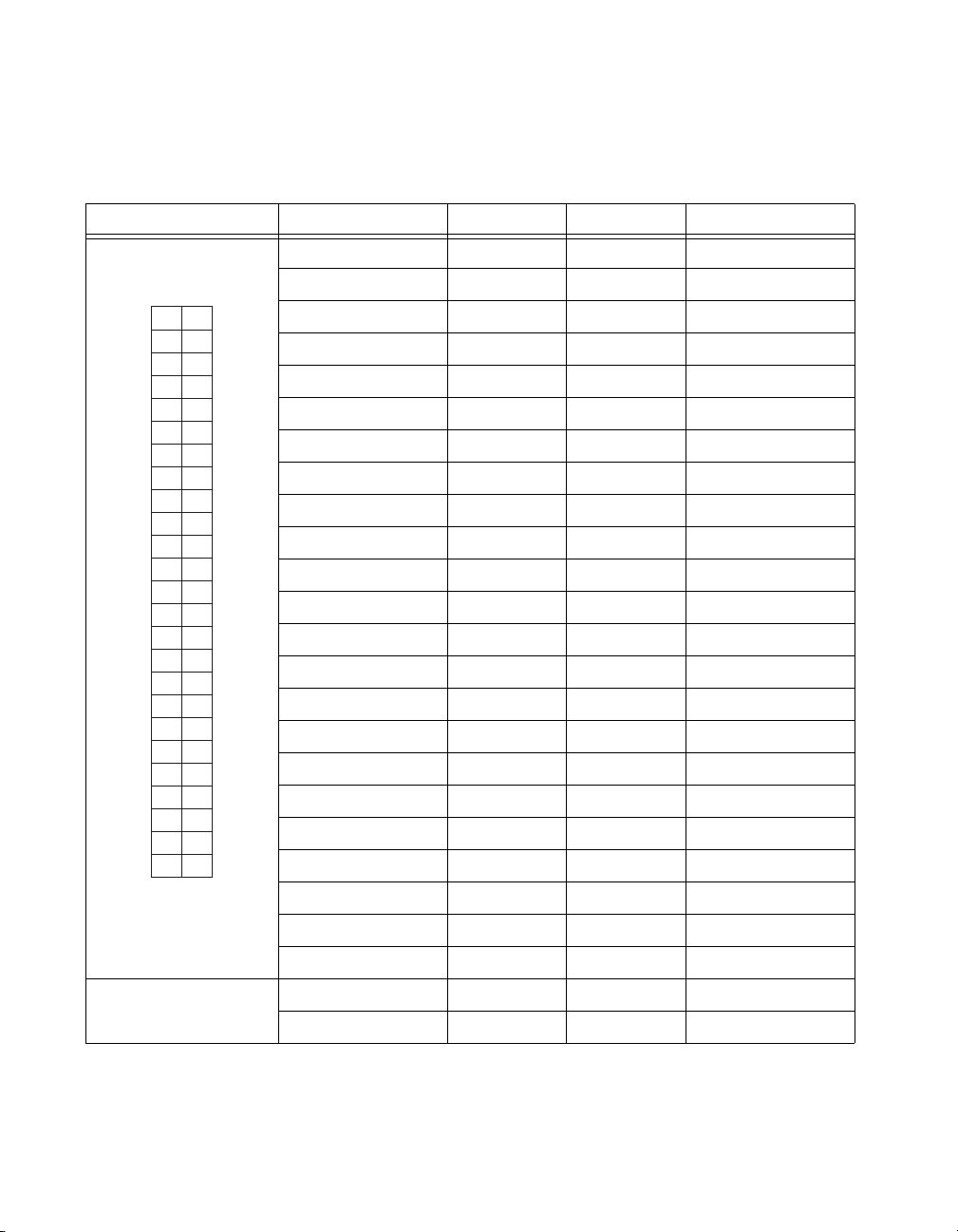
Table 2-1 shows the pin assignments for the SCXI-1141/1142/1143
module front connector.
2
© National Instruments Corporation 2-1 SCXI-1141/1142/1143 User Manual
Page 16

Chapter 2 Connecting Signals
Table 2-1. Front Signal Pin Assignments
Front Connector Diagram Pin Number Column A Column B Column C
32 AI 0 + NC AI 0 –
Column
A B C
32
31
30
29
28
27
26
25
24
23
22
21
20
19
18
17
16
15
14
13
12
11
10
9
8
7
6
5
4
3
2
1
NC means no connection.
RSVD means reserved.
31 NC NC NC
30 AI 1 + NC AI 1 –
29 NC NC NC
28 A GND NC A GND
27 NC NC NC
26 AI 2 + NC AI 2 –
25 NC NC NC
24 AI 3 + NC AI 3 –
23 NC NC NC
22 A GND NC A GND
21 NC NC NC
20 AI 4 + NC AI 4 –
19 NC NC NC
18 AI 5 + NC AI 5 –
17 NC NC NC
16 A GND NC A GND
15 NC NC NC
14 AI 6 + NC AI 6 –
13 NC NC NC
12 AI 7 + NC AI 7 –
11 NC NC NC
10 NC NC NC
9 NC NC NC
8 RSVD NC RSVD
7 NC NC NC
6 RSVD NC RSVD
5 NC NC NC
4 RSVD NC EXT CLK
3 NC NC NC
2 D GND NC OUT CLK
1 NC NC NC
SCXI-1141/1142/1143 User Manual 2-2 ni.com
Page 17

Front Connector Signal Descriptions
Pins Signal Names Description
Chapter 2 Connecting Signals
A32, A30, A26, A24,
A20, A18, A14, A12
C32, C30, C26, C24,
C20, C18, C14, C12
A28, A22, A16, C28,
C22, C16
A2, C8 D GND Digital ground—these pins connect to the module
A8, A6, A4, C8 RSVD Reserved—do not connect any signals to these pins.
C4 EXT CLK External clock—you can use this signal to set the
C2 OUT CLK Output clock—this signal has a frequency that is
Note: All other pins are not connected.
AI+<0..7+> Positive input channels—these pins connect to the
noninverting inputs of the instrumentation amplifier
of each channel.
AI–<0..7–> Negative input channels—these pins connect to the
inverting inputs of the instrumentation amplifier of
each channel.
A GND Analog ground—these pins connect to the module
analog ground.
digital ground.
filter cutoff frequency.
proportional to the cutoff frequency. You can use this
signal to externally control the cutoff frequency.
Analog Input Channels
The SCXI-1141/1142/1143 module instrumentation amplifiers can reject
any common-mode voltage within their common-mode input range caused
by ground-potential differences between the signal source and the module.
In addition, the amplifiers can reject common-mode noise pickup in the
leads connecting the signal sources to the SCXI-1141/1142/1143 module.
However, you should take care to minimize noise pickup. The
common-mode rejection of the instrumentation amplifiers decreases
significantly at high frequencies. The amplifiers do not reject
normal-mode noise.
The maximum differential input voltage range of the
SCXI-1141/1142/1143 module instrumentation amplifiers is a function of
the gain of the amplifiers, G, and is equal to 5 V/G. The common-mode
input range of the SCXI-1141/1142/1143 module, however, is not a
function of gain—the differential input amplifier rejects common-mode
signals as long as the signal at both inputs is within ±5 V of the module
© National Instruments Corporation 2-3 SCXI-1141/1142/1143 User Manual
Page 18
Chapter 2 Connecting Signals
Caution Exceeding the differential or common-mode input voltage limits distorts input
signals. Exceeding the maximum common-mode input voltage rating can damage the
SCXI-1141/1142/1143 module, the SCXIbus, and the DAQ device. NI is not liable for any
damage resulting from such signal connections.
Note The recommended SCXI-1304 or SCXI-1305 terminal block has all necessary
circuitry for AC or DC coupling and for floating or ground-referenced signals. The
SCXI-1304 AC/DC Coupling Terminal Block Installation Guide and SCXI-1305 AC/DC
Coupling BNC Terminal Block Installation Guide have instructions for signal connection.
Figures 2-2 through 2-5 provide supplemental information on connecting signals to the
SCXI-1141/1142/1143 module.
analog ground. The inputs are protected against maximum input voltages
of up to ±15 V powered off and ±30 V powered on.
All eight channels have fully differential inputs, so you can
ground-reference the signals you measure. If the signals connected to the
differential amplified inputs are not ground referenced, connect a 100 kΩ
resistor from the negative input to ground to provide a DC path for the input
bias currents. If you do not do this, the bias currents of the instrumentation
amplifiers of the nonreferenced channels charge up stray capacitances,
resulting in uncontrollable drift and possible saturation.
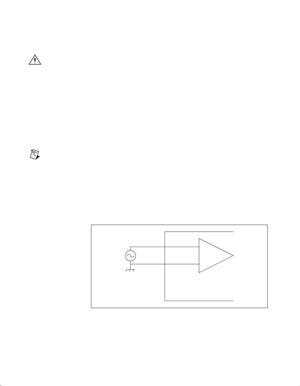
Figure 2-1 illustrates how to connect a ground-referenced signal source to
an SCXI-1141/1142/1143 module channel.
IN+
IN–
SCXI-1141/1142/1143
Figure 2-1. Ground-Referenced Signal Connection
SCXI-1141/1142/1143 User Manual 2-4 ni.com
Page 19

Chapter 2 Connecting Signals
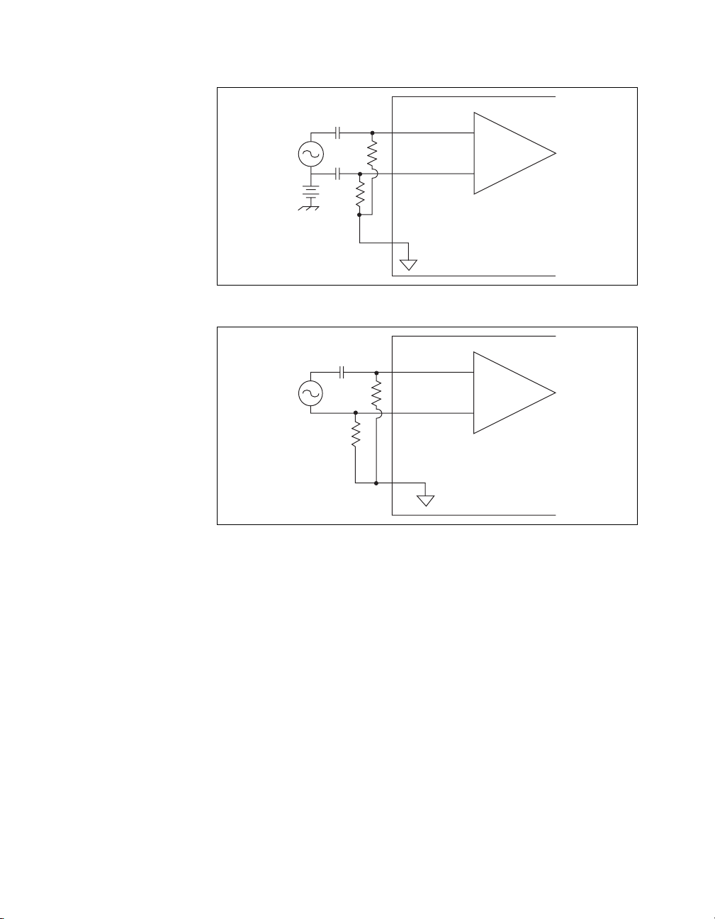
Figure 2-2 illustrates how to connect a non-referenced (floating) signal
source to an SCXI channel.
IN+
IN–
100 kΩ
SCXI-1141/1142/1143
A GND
A
Figure 2-2. Floating Signal Connection
For AC-coupled signals, connect an external resistor from the AC-coupled
input channel to ground. This provides a DC path for the amplifier input
bias current. Typical resistor values range from 100 kΩ to 10 MΩ . This
solution, although necessary, lowers the input impedance of the channel
and introduces an additional DC offset voltage proportional to the product
of the input bias current and the resistor value used. Using a 1 MΩ resistor
results in ±200 µV of offset, which is insignificant in most applications.
However, if you use larger-valued bias resistors, significant input offset can
result. Lower-valued bias resistors increase loading of the source, which
can result in gain error.
Figures 2-3 through 2-5 illustrate how to connect AC-coupled signals.
1µF
IN+
1MΩ
IN–
SCXI-1141/1142/1143
Figure 2-3. Ground-Referenced AC-Coupled Signal Connection
© National Instruments Corporation 2-5 SCXI-1141/1142/1143 User Manual
Page 20
Chapter 2 Connecting Signals
1 µF
1 µF
1
MΩ
1 MΩ
A GND
A
IN+
IN–
SCXI-1141/1142/1143
Figure 2-4. Ground Offset AC-Coupled Signal Connection
1 µF
100 kΩ
1 MΩ
A GND
A
IN+
IN–
SCXI-1141/1142/1143
Figure 2-5. Floating AC-Coupled Signal Connection
Digital Input and Output
You can use the EXT CLK input pin on the front connector of the
SCXI-1141/1142/1143 module to control filter cutoff frequency for special
purposes. The clock should be a TTL-logic-level or CMOS-logic-level
square wave, with a frequency of less than 2.5 MHz that is 100 times the
desired cutoff frequency. The absolute maximum input voltage for the
EXT CLK pin is 5.5 V with respect to D GND; the minimum input voltage
is –0.5 V.
The OUT CLK pin on the front connector is a CMOS-logic-level output
clock, which you can configure to have a frequency that is proportional to
filter cutoff frequency.
See Chapter 4, Theory of Operation, for more details on using these
two signals.
SCXI-1141/1142/1143 User Manual 2-6 ni.com
Page 21

Rear Signal Connector
Note If you use the SCXI-1141/1142/1143 module with a National Instruments DAQ
device and SCXI cable assembly, you do not need to read the remainder of this chapter.
If you also use the SCXI-1180 feedthrough panel, the SCXI-1343 rear screw-terminal
adapter, or the SCXI-1351 one-slot cable extender with the SCXI-1141/1142/1143
module, you should read this section.
Chapter 2 Connecting Signals
© National Instruments Corporation 2-7 SCXI-1141/1142/1143 User Manual
Page 22
Chapter 2 Connecting Signals
Table 2-2 shows the pin assignments for the SCXI-1141/1142/1143 module
rear signal connector. Pins without signal labels are not connected.
Table 2-2. Rear Signal Pin Assignments
Rear Connector Diagram Signal Name Pin Number Pin Number Signal Name
NC 1 2 NC
AI 0 + 3 4 AI 0 –
12
34
56
78
910
11 12
13 14
15 16
17 18
19 20
21 22
23 24
25 26
27 28
29 30
31 32
33 34
35 36
37 38
39 40
41 42
43 44
45 46
47 48
49 50
AI 1 + 5 6 A GND
AI 2 + 7 8 A GND
AI 3 + 9 10 A GND
AI 4 + 11 12 A GND
AI 5 + 13 14 A GND
AI 6 + 15 16 A GND
AI 7 + 17 18 A GND
NC 19 20 NC
NC 21 22 NC
NC 23 24 DIG GND
SER DAT IN 25 26 SER DAT OUT
DAQ D*/A 27 28 NC
SLOT 0 SEL* 29 30 NC
NC 31 32 NC
DIG GND 33 34 NC
NC 35 36 SCAN CLK
SER CLK 37 38 NC
NC 39 40 NC
NC 41 42 NC
RSVD 43 44 NC
NC 45 46 NC
NC means no connection.
RSVD means reserved.
SCXI-1141/1142/1143 User Manual 2-8 ni.com
NC 47 48 NC
NC 49 50 NC
Page 23

Pin
Table 2-3. SCXI-1141/1142/1143 Rear Communication Signals
SCXI Signal
Name
Chapter 2 Connecting Signals
In parallel output mode, channel 0 is selected at the output multiplexer and
is connected to AI 0. The seven other channels are directly connected to
AI 1 through AI 7, respectively, on the rear connector.
In multiplexed mode, the AI 0 signal pair is used for sending all eight
channels of the SCXI-1141/1142/1143, and analog signals from other
modules, to the connected E/M Series DAQ device. If the module is cabled
directly to the DAQ device, the other analog channels of the DAQ device
are unavailable for general-purpose analog input because they are
connected to the SCXI-1141/1142/1143 amplifier outputs. This means that
connecting an SCXI-1180 module to the 50-pin breakout connector of the
SCXI-1349, or other cable adapter assembly, may cause interference and
incorrect measurements when the DAQ device is cabled to the
SCXI-1141/1142/1143.
The communication signals between the DAQ device and the SCXI system
are listed in Table 2-3. If the DAQ device is connected to the
SCXI-1141/1142/1143, these digital lines are unavailable for
general-purpose digital I/O.
NI-DAQmx
Device Signal
Name
Direction Description
5, 7, 9,
11, 13,
15, 17
6, 8,
10, 12,
14, 16,
18
24,
33
AI <1..7> N/A Output Analog outputs—these pins are the
outputs of channels 1 through 7,
regardless of the scanning mode.
A GND AI GND — Analog ground—these pins connect
to the module analog ground. They
are used as the reference points for
AI 1 + through AI 7 +.
DIG GND D GND — Digital ground—these pins supply
the reference for E/M Series DAQ
device digital signals and connect to
the module digital ground.
25 SER DAT IN P0.0 Input Serial data in—this signal taps into
the SCXIbus MOSI line to send
serial input data to a module or
Slot 0.
© National Instruments Corporation 2-9 SCXI-1141/1142/1143 User Manual
Page 24

Chapter 2 Connecting Signals
Table 2-3. SCXI-1141/1142/1143 Rear Communication Signals (Continued)
NI-DAQmx
Device Signal
Name
Direction Description
Pin
SCXI Signal
Name
26 SER DAT OUT P0.4 Output Serial data out—this signal taps into
the SCXIbus MISO line to accept
serial output data from a module.
27 DAQ D*/A P0.1 Input Board data/address line—this signal
taps into the SCXIbus D*/A line to
indicate to the module whether the
incoming serial stream is data or
address information.
29 SLOT 0 SEL* P0.2 Input Slot 0 select—this signal taps into
the SCXIbus INTR* line to indicate
whether the information on MOSI is
being sent to a module or Slot 0.
36 SCAN CLK AI HOLD,
AI HOLD COMP
Input Scan clock—a rising edge indicates
to the scanned SCXI module that the
E/M Series DAQ device has taken a
sample and causes the module to
advance channels.
37 SER CLK EXT STROBE* Input Serial clock—this signal taps into
the SCXIbus SPI CLK line to clock
the data on the MOSI and MISO
lines.
43 RSVD RSVD Input Reserved.
Notes: All other pins are not connected.
An * means the signal is asserted low.
The signals on the rear signal connector are classified as analog output,
digital I/O, or timing I/O signals.
SCXI-1141/1142/1143 User Manual 2-10 ni.com
Page 25

Analog Output Signal Connections
Pins 3 through 17 of the rear signal connector are analog output signal pins.
Pin 3 is the main output, and pin 4 is its reference signal. All eight channels
are multiplexed onto this output when the module is software-configured
for multiplexed scanning mode. In parallel scanning mode, the output of
pin 3 is the output of one selected channel. Channel 0 is the power-up and
reset default. When scanning multiple modules, you can also connect this
output to the SCXIbus analog bus and the analog bus will drive this output.
Pins 5, 7, 9, 11, 13, 15, and 17 are direct outputs from channels 1 through 7,
respectively. In parallel mode, all eight channels are available
simultaneously at the rear connector. Pins 6, 8, 10, 12, 14, 16, and 18 are
the reference signals for outputs 1 through 7.
Caution The SCXI-1141/1142/1143 module analog outputs are not overvoltage protected,
although they are short-circuit protected. Applying external voltage to these outputs can
result in damage to the SCXI-1141/1142/1143 module. NI is not liable for any damage
resulting from such signal connections.
Digital I/O Signal Connections
Pins 24 through 27, 29, 33, 36, 37, and 43 constitute the digital I/O lines
of the rear signal connector. Each of these pins is in one of three
categories—digital input signals, digital output signals, and timing signals.
Pins 24 and 33 are the digital ground reference for all of the DAQ device
digital signals and are tied to the module digital ground.
Chapter 2 Connecting Signals
The digital input signals are pins 25, 27, 29, and 37. Each digital line
emulates an SCXIbus communication signal as follows:
• Pin 25 is SER DAT IN and is equivalent to the SCXIbus MOSI serial
data input line.
• Pin 27 is DAQ D*/A and is equivalent to the SCXIbus D*/A line.
Pin 27 indicates to the module whether the incoming serial stream on
SER DAT IN is data (DAQ D*/A = 0) or address (DAQ D*/A = 1)
information.
• Pin 29 is SLOT 0 SEL* and is equivalent to the SCXIbus INTR* line.
Pin 29 indicates whether the data on the SER DAT IN line is being sent
to Slot 0 (SLOT 0 SEL* = 0) or to a module (SLOT 0 SEL* = 1).
• Pin 37 is SER CLK and is equivalent to the SCXIbus SPI CLK line.
Pin 37 is used to clock the serial data on the SER DAT IN line into the
module registers.
© National Instruments Corporation 2-11 SCXI-1141/1142/1143 User Manual
Page 26

Chapter 2 Connecting Signals
The digital output signal is pin 26. Pin 26 is SER DAT OUT and is
equivalent to the SCXIbus MISO serial data output line.
The digital I/O signals of the SCXI-1141/1142/1143 module correspond
to the digital I/O lines of an E/M Series DAQ device. Table 2-4 lists the
equivalencies.
Table 2-4. SCXIbus to SCXI-1141/1142/1143 Module Rear Signal Connector
to DAQ Device Pin Equivalencies
SCXIbus Line
SCXI-1141/1142/1143
Rear Signal Connector
E/M Series
DAQ Device
MOSI SER DAT IN DIO0
D*/A DAQ D*/A DIO1
INTR* SLOT 0 SEL* DIO2
SPI CLK SER CLK EXT STROBE*
MISO SER DAT OUT DIO4
Note: An * means the signal is asserted low.
The digital timing signals are pins 36 and 43:
• Pin 36 is SCAN CLK, the signal used as a clock for the
SCXI-1141/1142/1143 module multiplexer counter. The DAQ device
pulses this signal at the end of each conversion if the module is in
multiplexed mode.
• Pin 43 is a reserved digital input.
SCXI-1141/1142/1143 User Manual 2-12 ni.com
Page 27

3
Configuring and Testing
This chapter discusses configuring the SCXI-1141/1142/1143 in MAX
using NI-DAQmx, creating and testing a virtual channel, global channel,
and/or task.
Notes NI recommends that you have NI-DAQmx 8.3 or later installed.
Refer to the SCXI Quick Start Guide if you have not already configured the chassis.
SCXI-1141/1142/1143 Software-Configurable Settings
This section describes how to set the gain/input signal range and how to
configure your software for compatible sensor types. It also describes how
to perform configuration of these settings for the SCXI-1141/1142/1143 in
NI-DAQmx. For more information on the relationship between the settings
and the measurements and how to configure settings in your application,
refer to Chapter 4, Theory of Operation.
Common Software-Configurable Settings
This section describes the most frequently used software-configurable
settings for the SCXI-1141/1142/1143. Refer to Chapter 4, Theory of
Operation, for a complete list of software-configurable settings.
Gain/Input Range
Gain/input range is a software-configurable setting that allows you to
choose the appropriate amplification to fully utilize the range of the
E/M Series DAQ device. In most applications NI-DAQ chooses and sets
the gain for you determined by the input range. This feature is described in
Chapter 4, Theory of Operation. Otherwise, you should determine the
appropriate gain using the input signal voltage range and the full-scale
limits of the SCXI-1141/1142/1143 output. You can select a gain of 1, 2, 5,
10, 20, 50, or 100 on a per channel basis.
© National Instruments Corporation 3-1 SCXI-1141/1142/1143 User Manual
Page 28

Chapter 3 Configuring and Testing
Input Selection
The front end of the SCXI-1141/1142/1143 includes a software
configurable switch that allows you to programmatically connect the input
channels of the SCXI-1141/1142/1143 to either the front connector or
internal ground. Refer to Table 5-1, NI-DAQmx Voltage Measurement
Properties, for details about the available input coupling modes supported
by the SCXI-1141/1142/1143.
Auto-Zero
Setting the Auto-zero mode to Once improves the accuracy of
the measurement. With auto-zero enabled, the inputs of the
SCXI-1141/1142/1143 are internally grounded. The driver makes a
measurement when the task begins and then subtracts the measured offset
from all future measurements.
Although the DAQ driver does wait a certain amount of time for the signal
to settle, it may not be long enough if the filter is set to very low cutoff
frequency. This is especially true if the voltage ever goes out of range and
the amplifier becomes saturated. You can manually zero out the offset by
comparing the ground coupled value of a channel to its DC coupled value,
then subtracting that offset from future measurements. This allows you to
control the time allowed for the signals to settle.
Configurable Settings in MAX
Note If you are not using an NI ADE, using an NI ADE prior to version 8.3, or are using
an unlicensed copy of an NI ADE, additional dialog boxes from the NI License Manager
appear allowing you to create a task or global channel in unlicensed mode. These messages
continue to appear until you install version 8.3 or later of an NI ADE.
This section describes where you can access each software-configurable
setting in MAX. The location of the settings varies depending on the
version of NI-DAQmx you use. Refer to the DAQ Getting Started Guide
and the SCXI Quick Start Guide for more information on installing and
configuring the hardware. You can use DAQ Assistant to graphically
configure common measurement tasks, channels, or scales.
SCXI-1141/1142/1143 User Manual 3-2 ni.com
Page 29

NI-DAQmx
Note All software-configurable settings are not configurable both ways. This section only
discusses settings in MAX. Refer to Chapter 4, Theory of Operation, for information about
using functions in your application.
Chapter 3 Configuring and Testing
Using NI-DAQmx, you can configure software settings, such as sensor
type and gain/input signal range, in the following ways:
• Task or global channel in MAX
• Functions in your application
Depending on the terminal block in use, you can use the
SCXI-1141/1142/1143 module to make the following types of
measurements:
• Voltage input
• Thermocouple
•RTD
• Thermistors
• Current input
Creating a Global Channel or Task
To create a new voltage, temperature, or current input NI-DAQmx global
task or channel, complete the following steps:
1. Double-click Measurement & Automation on the desktop.
2. Right-click Data Neighborhood and select Create New.
3. Select NI-DAQmx Task or NI-DAQmx Global Channel, and
click Next.
4. Select Analog Input.
5. Select one of the following:
• Voltage
• Temperature and then select one of the following:
– Iex Thermistor
– RTD
– Thermocouple
– Vex Thermistor
• Current
© National Instruments Corporation 3-3 SCXI-1141/1142/1143 User Manual
Page 30

Chapter 3 Configuring and Testing
6. If you are creating a task, you can select a range of channels by holding
7. Name the task or channel and click Finish.
8. Select the channel(s) you want to configure. You can select a range
Note If you want to add channels of various measurement types to the same task, click
the Add Channels button to select the measurement type for the additional channels.
9. Enter the specific values for your application in the Settings tab.
10. If you are creating a task and want to set timing or triggering controls,
11. Click Device and select Auto Zero mode if desired.
down the <Shift> key while selecting the channels. You can select
multiple individual channels by holding down the <Ctrl> key while
selecting channels. If you are creating a channel, you can only select
one channel. Click Next.
of channels by holding down the <Shift> key while selecting the
channels. You can select multiple individual channels by holding down
the <Ctrl> key while selecting channels.
Context help information for each setting is provided on the right
side of the screen. Configure the input signal range using either
NI-DAQmx Task or NI-DAQmx Global Channel. When you set the
minimum and maximum range of NI-DAQmx Task or NI-DAQmx
Global Channel, the driver selects the best gain for the measurement.
You also can set it through your application.
enter the values in the Task Timing and Task Triggering tabs.
Verifying the Signal
This section describes how to take measurements using test panels in order
to verify signal, and configuring and installing a system in NI-DAQmx.
Verifying the Signal in NI-DAQmx Using a Task or Global Channel
You can verify the signals on the SCXI-1141/1142/1143 using NI-DAQmx
by completing the following steps:
1. Expand Data Neighborhood.
2. Expand NI-DAQmx Tasks.
3. Click the task you created in the Creating a Global Channel or Task
section.
SCXI-1141/1142/1143 User Manual 3-4 ni.com
Page 31

Chapter 3 Configuring and Testing
4. Select the channel(s) you want to verify. You can select a block of
channels by holding down the <Shift> key or multiple channels by
holding down the <Ctrl> key. Click OK.
5. Enter the appropriate information on the Settings and Device tab.
6. Click the Test button.
7. Click the Start button.
8. After you have completed verifying the channels, click the Stop
button.
You have now verified the SCXI-1141/1142/1143 configuration and signal
connection.
Note For more information on how to further configure the SCXI-1141/1142/1143, or
how to use LabVIEW to configure the module and take measurements, refer to Chapter 4,
Theory of Operation.
© National Instruments Corporation 3-5 SCXI-1141/1142/1143 User Manual
Page 32

Theory of Operation
This chapter contains an overview of the SCXI-1141/1142/1143 module
and explains the operation of each functional unit of the module.
The SCXI-1141/1142/1143 module has eight software-controlled input
channels that amplify and filter signals. Each channel has an output range
of ±5 V and has an input amplifier with gains of 1, 2, 5, 10, 20, 50, and 100.
You can independently set each amplifier gain. The analog inputs are
overvoltage protected. The SCXI-1141/1142/1143 module filters are
lowpass, 8th-order elliptic, Bessel, and Butterworth filters respectively that
can have a cutoff frequency from 10 Hz to 25 kHz. All eight filters have the
same cutoff frequency. The outputs of all eight channels are available at the
rear connector.
The major components of the SCXI-1141/1142/1143 module are as
follows:
• Digital control and calibration circuitry
• Input amplifiers
• Lowpass filters
4
Power-Up State
When the SCXI-1141/1142/1143 module is powered up or reset through
software or the SCXI chassis reset button, the following states are defined:
• The gain of each amplifier is set to 1.
• Channel 0 is selected as the OUTPUT signal and the module defaults
to multiplexed mode.
• All filters are placed in bypass mode.
• The external clock input is disabled.
The cutoff frequency of the filters and the output clock frequency are not
defined at power-up.
The block diagram in Figure 4-1 illustrates the key functional components
of the SCXI-1141/1142/1143 module.
© National Instruments Corporation 4-1 SCXI-1141/1142/1143 User Manual
Page 33

Chapter 4 Theory of Operation
AI 0+
Input
AI 0–
Protection
Front Signal Connector
AI 7+
Input
AI 7–
Protection
Internal
16-Pin Analog
Input Connector
+
Instrumentation
–
Selection
Calibration
+
Instrumentation
–
Selection
Calibration
External Clock
Output Clock
Calibration
EEPROM
Amplifier
Amplifier
Filter
Filter
Filter
Bypass
Filter
Bypass
Digital
Interface
and Control
AI 0
AI 7
Analog
AI 0
Switch
8 to 1 Multiplexer
Analog
Switch
AI 7
Rear Signal Connector
Analog Bus
Digital Control Bus
SCXIbus Connector
Figure 4-1. SCXI-1141/1142/1143 Module Block Diagram
SCXI-1141/1142/1143 User Manual 4-2 ni.com
Page 34

Digital Control Circuitry
The digital control circuitry contains a Module ID (identification) register,
a configuration register for the module, a gain register, and an EEPROM
for storing gain-calibration constants.
The Module ID register contains 20 (hex) for the SCXI-1141 module,
35 (hex) for the SCXI-1142 module, and 34 (hex) for the SCXI-1143
module. You can read this module ID over the SCXIbus to determine the
type of module that is in a particular slot.
Use the configuration register to select channels and configure the
SCXI-1141/1142/1143 module for scanning, calibration, and control
options.
The gain register sets the gain of each amplifier.
The frequency dividers control the filter cutoff frequency and the output
clock frequency. For more information see the Using the External Clock
Input section.
The EEPROM stores the calibration constants for each gain for all eight
channels. Information in the EEPROM is retained when the module is
power off. The SCXI-1141/1142/1143 module has calibration constants
already stored in the EEPROM. You can modify these constants for your
set of operating conditions. One set of constants is reserved and cannot be
modified except at the factory, which ensures that you do not accidentally
erase the default calibration constants. For more information on the
EEPROM and calibration, see Chapter 5, Using the SCXI-1141/1142/1143
Module.
Chapter 4 Theory of Operation
Input Amplifiers
The amplifiers provide gain to the differential signal between the inputs
while rejecting common-mode noise voltages. The available gains are 1, 2,
5, 10, 20, 50, and 100. The output range of the amplifiers is ±5 V. Select
the gain to prevent the output signals from reaching ±5 V, or distortion
occurs.
The input amplifiers are fully differential amplifiers with input protection
and calibration circuitry. The inputs are protected against input voltages up
to ±15 V powered off and ±30 V powered on.
© National Instruments Corporation 4-3 SCXI-1141/1142/1143 User Manual
Page 35

Chapter 4 Theory of Operation
In general, to provide optimum measurement resolution and noise
rejection, you can select as high a gain as will not cause the output to exceed
this limit. However, total harmonic distortion (THD) increases at higher
output levels, especially at higher input frequencies. If THD is of
significant concern in a given application, a lower gain (one or two steps
lower) may be more appropriate.
Correcting Gain and Offset Errors
The input amplifiers have intrinsic errors in their gains and in their DC
offsets. To compensate for the gain errors, calibration constants are stored
in the EEPROM for each gain and for each channel. These constants
contain the adjustment factors used to correct for the gain errors. If you are
using NI software, these constants are read automatically from the
EEPROM and the appropriate correction factor is applied when the raw
data is scaled to a voltage.
Gain errors are determined and calibration constants are loaded into the
EEPROM at the factory. However, gain errors drift with temperature
changes. You can add an additional set or subset of calibration constants to
the EEPROM to optimize performance under a specific set of conditions.
Details of this procedure are given in Chapter 5, Using the
SCXI-1141/1142/1143 Module.
To account for offset errors, you can configure the module to send a 0 V
differential signal through the amplifiers. The signal at the output
represents the DC offset error and should be read and subtracted from all
subsequent readings. Before reading this offset error on a channel, either set
the filter to bypass mode or allow it to settle for several seconds. Average
several readings to minimize noise errors. This procedure is called
calibration.
Because the offset voltage changes with each gain, you should perform a
new calibration each time the gain is changed. Offset errors also drift with
changes in temperature, so you should update the offset correction
periodically. Measurements made during the warm-up period of the module
(approximately 20 minutes) and chassis are most susceptible to drifting
offset errors.
SCXI-1141/1142/1143 User Manual 4-4 ni.com
Page 36

Lowpass Filters
Filter Theory
Chapter 4 Theory of Operation
The SCXI-1141/1142/1143 module filters are 8th-order elliptic, Bessel,
and Butterworth lowpass filters, respectively. These filters are a hybrid of
a switched-capacitor and a continuous-time architecture, thus providing
good cutoff frequency control while avoiding the sampling errors found in
conventional switched-capacitor designs. To better acquaint you with these
filters, this section describes what the filters do and presents examples of
how to use them on the SCXI-1141/1142/1143 module.
Filters are generally grouped into one of five classifications—lowpass,
highpass, bandpass, bandstop, and all-pass. These classifications refer
to the frequency range (the passband) of signals that the filter is intended
to pass from the input to the output without attenuation. Because the
SCXI-1141/1142/1143 modules use a lowpass filter, this discussion is
limited to lowpass filters.
The ideal lowpass filter does not attenuate any input signal frequency
components in the passband, which is defined as all frequencies below the
cutoff frequency. The ideal lowpass filter completely attenuates all signal
components in the stopband, which includes all frequencies above the
cutoff frequency. The ideal lowpass filter also has a phase shift that is linear
with respect to frequency. This linear phase property means that signal
components of all frequencies are delayed by a constant time independent
of frequency, thereby preserving the overall shape of the signal.
In practice, real filters can only approximate the characteristics of an ideal
filter. Figure 4-2 compares the attenuation of a real filter and an ideal filter.
Passband
Gain
Stopband
f
c
Frequency
a. Ideal b. Real
Figure 4-2. Ideal and Real Lowpass Filter Transfer Function Characteristics
© National Instruments Corporation 4-5 SCXI-1141/1142/1143 User Manual
Gain
Passband
f
c
Frequency
Transition
Region
Stopband
Page 37

Chapter 4 Theory of Operation
As Figure 4-2b shows, a real filter has ripple (an uneven variation in
attenuation versus frequency) in the passband, a transition region between
the passband and the stopband, and a stopband with finite attenuation and
ripple.
In addition, real filters have some nonlinearity in their phase response. This
causes signal components at higher frequencies to be delayed by longer
times than signal components at lower frequencies, resulting in an overall
shape distortion of the signal. You can observe this when a square wave or
step input is sent through a lowpass filter. An ideal filter simply smooths the
edges of the input signal, whereas a real filter causes some ringing in the
total signal because the higher-frequency components of the signal are
delayed. Figure 4-3 shows examples of these responses to a step input.
Vol tsVol ts
Time Time
b. Ideal Filter Responsea. Input Signal
Figure 4-3. Real and Ideal Filter Responses to a Step Input Signal
Vol ts
c. Real Filter Response
Performance of the SCXI-1141/1142/1143 Module Filters
The SCXI-1141/1142/1143 module is elliptic, Bessel, and Butterworth
filters, respectively. Each filter design optimizes a particular set of
characteristics. Therefore, selecting the appropriate module depends on
the application.
Magnitude Response
The magnitude response is the amplitude of the output at a given frequency.
The typical magnitude response of the SCXI-1141/1142/1143 module
filters is shown in Figures 4-4 and 4-5. Figure 4-4 shows the full magnitude
response and Figure 4-5 shows the ripple in the passband. Both graphs are
plotted with the frequency axis normalized to the cutoff frequency value
of 1.
Time
SCXI-1141/1142/1143 User Manual 4-6 ni.com
Page 38

Chapter 4 Theory of Operation
As Figure 4-4 shows, the SCXI-1141/1142/1143 module provides 80 dB
attenuation above 1.5 times the cutoff frequency for the SCXI-1141
module, six times for the SCXI-1142 module, and 3.2 times for the
SCXI-1143 module. The SCXI-1141, which incorporates an elliptic filter,
is designed to provide maximum attenuation immediately above the cutoff
frequency. Therefore, it is the ideal choice for applications in which you
must remove signals very near the cutoff frequency.
50
0
Elliptic (1141)
Bessel (1142)
Butterworth (1143)
–80 dB Intersection
–50
–80
Gain (dB)
–100
–150
–200
1 x 10
–3
0.01 0.1 1 10
Frequency (Normalized)
Figure 4-4. Typical Magnitude Response of the SCXI-1141/1142/1143 Module Filters
Figure 4-5 compares the magnitude response of the SCXI-1141/1142/1143
modules within the passband. The passband magnitude response begins to
drop off immediately for the SCXI-1142 module. The SCXI-1141 performs
much better than the SCXI-1142 in the passband, but it still exhibits about
0.1 dB of ripple in magnitude in the passband. The SCXI-1143 module
Butterworth filter is designed for maximum flatness in the passband and is
nearly perfectly flat in most of the passband. For this reason the SCXI-1143
module filter is the ideal choice for applications where flatness in the
passband is critical.
© National Instruments Corporation 4-7 SCXI-1141/1142/1143 User Manual
Page 39

Chapter 4 Theory of Operation
0.5
0
–0.5
Elliptic (1141)
Bessel (1142)
Butterworth (1143)
–1
–1.5
Gain (dB)
–2
–2.5
–3
–3.5
0 0.2 0.4 0.6 0.8 1
Frequency (Normalized)
Figure 4-5. Typical Passband Responses of the SCXI-1141/1142/1143 Module
Phase Response
Figures 4-6 through 4-8 illustrate the phase response characteristics of the
SCXI-1141/1142/1143 module filters. Figure 4-6 shows the phase shift as
a function of frequency (normalized so that the cutoff frequency = 1). In an
ideal filter, this would be a linear relationship. Figure 4-7 shows the
deviation of the actual phase response from an ideal (linear) response.
Generally, phase response is described in terms of the differential
nonlinearity, or group delay. Group delay is defined as the negative
derivative of the phase shift with respect to the frequency. In the ideal filter,
group delay is a constant.
SCXI-1141/1142/1143 User Manual 4-8 ni.com
Page 40

Elliptic (1141)
Bessel (1142)
Butterworth (1143)
Chapter 4 Theory of Operation
0
–200
–400
Phase Shift (Degrees)
–600
–800
0 0.5 1 1.5 2
Frequency (Normalized)
Figure 4-6. Phase Response Characteristics of the SCXI-1141/1142/1143
Module Filters
Figure 4-7 shows the advantages of the SCXI-1142 Bessel filter. The
Bessel filter is designed for constant group delay at the expense of passband
gain and stopband rolloff. As a result, the SCXI-1142 Bessel filter is the
best choice when the phase information of a signal is important or a signal
must maintain a constant delay regardless of its frequency components.
© National Instruments Corporation 4-9 SCXI-1141/1142/1143 User Manual
Page 41

Chapter 4 Theory of Operation
Elliptic (1141)
Bessel (1142)
Butterworth (1143)
300
200
100
Phase Error (Degrees)
0
–100
0 0.5 1 1.5 2
Frequency (Normalized)
Figure 4-7. Phase Error of the SCXI-1141/1142/1143 Module
The most common effect of phase nonlinearity is ringing in response to a
step input. As Figure 4-8 shows, the SCXI-1141 elliptic filter exhibits the
most overshoot and ringing and the SCXI-1142 Bessel filter has no
overshoot or ringing. The SCXI-1143 module Butterworth filter has a step
response that is a compromise between the SCXI-1141 module and the
SCXI-1142 module. The SCXI-1143 module filter has an overshoot, but it
has less ringing than the SCXI-1141. You should consider the step response
if the intended application is sensitive to overshoot or ringing. See
Tabl e A-1, Settling Time with Respect to Cutoff Frequency, for detailed
settling specifications. Additionally, use care when selecting gain settings
to assure that the input signal plus any overshoot voltage result in an output
signal within the ±5 V range of the SCXI-1141/1142/1143 module.
SCXI-1141/1142/1143 User Manual 4-10 ni.com
Page 42

1.4
f
1.2
Chapter 4 Theory of Operation
1
Elliptic (1141)
Bessel (1142)
Butterworth (1143)
0.8
0.6
Output Voltage (V)
0.4
0.2
0
0246 810
Time (Seconds)
Figure 4-8. Unit Step Response of the SCXI-1141/1142/1143 Module
Setting the Cutoff Frequency
The cutoff frequencies of the filters in the SCXI-1141/1142/1143 module
are set internally by dividing a base frequency of 100 kHz by an integer.
You can determine the allowable cutoff frequencies for the
SCXI-1141/1142/1143 module as follows:
100
---------
c
kHz=
n
where n is an integer ≥ 4 and f
≥ 10 Hz. In other words, fc = {25, 20, 16.7,
c
14.3, 12.5, ..., 0.01} kHz.
If you are using NI software, the software automatically chooses a divisor,
n, that best matches the cutoff frequency you specify and returns the actual
cutoff frequency chosen.
The correct cutoff frequency depends on the application. If phase
nonlinearity, ringing, passband ripple, or aliasing is a concern in the
application, you may need to set the cutoff frequency several times higher
© National Instruments Corporation 4-11 SCXI-1141/1142/1143 User Manual
Page 43

Chapter 4 Theory of Operation
–
than the signal frequency range of interest. At frequencies much lower than
the cutoff frequency, passband ripple and phase nonlinearity are much less
noticeable. If you use the filter to prevent aliasing, you must set the cutoff
frequency no higher than one-third of the frequency at which that channel
is being sampled for the SCXI-1141 module, one-twelfth of the frequency
for the SCXI-1142 module, or one-sixth of the frequency for the
SCXI-1143 module.
Using the SCXI-1141/1142/1143 Module as an Antialiasing Filter
Aliasing, a phenomenon of sampled data acquisition systems, causes a
high-frequency signal component to take on the identity of a low-frequency
signal. Figure 4-9 shows an example of aliasing.
1
1
02 46 810
Input Signal
Sampled Point
Reconstructed Signal
Figure 4-9. Aliasing of an Input Signal with a Frequency 0.8 Times the Sample Rate
The solid line depicts a high-frequency signal being sampled at the
indicated points. However, when these points are connected to reconstruct
the waveform, as shown by the dotted line, the signal appears to have a
lower frequency. Any signal frequency with a frequency component greater
than one-half of the sample rate is aliased and incorrectly analyzed as
having a frequency below one-half of the sample rate. This limiting
frequency of one-half the sample rate is known as the Nyquist frequency.
To prevent aliasing, you must remove all signal components with
frequencies greater than the Nyquist frequency before sampling an input
signaled. After an unfiltered signal is sampled and aliasing has occurred,
it is impossible to accurately reconstruct the original signal. The
SCXI-1141/1142/1143 module removes these high-frequency signals
before they reach a DAQ device and cause aliasing.
SCXI-1141/1142/1143 User Manual 4-12 ni.com
Page 44

Chapter 4 Theory of Operation
Because the SCXI-1141 module stopband begins at 1.5 times the cutoff
frequency, the Nyquist frequency should be at least 1.5 times the cutoff
frequency. Thus, the rate at which the DAQ device samples a channel
should be at least three times the filter cutoff frequency to acquire
meaningful data.
The stopband for the SCXI-1142 module begins at six times the cutoff
frequency, so you should sample it at a rate of 12 times the cutoff frequency
to acquire meaningful data.
The stopband for the SCXI-1143 module begins at 3.2 times the cutoff
frequency, so you should sample it at a rate of 6.4 times the cutoff
frequency to acquire meaningful data.
For example, if a DAQ device is scanning all eight channels of the
SCXI-1141 at a rate of 120,000 channels/s, the sample rate for each of
the eight channels is:
120,000
------------------- 15,000 S/s=
8
and the cutoff frequency for the filters should be set no higher than:
15,000
---------------- 5,000 Hz=
3
Using this stopband, the filter attenuates the input signal by 80 dB or more.
This is enough attenuation to prevent aliasing on DAQ systems with 12 bits
of precision or less. On systems with more than 12 bits of precision or
systems with extremely high amounts of out-of-passband noise, higher
sampling rates or lower cutoff frequencies are necessary to prevent aliasing.
You can set the filter cutoff frequency closer to the sampling rate with the
consequence of having some aliasing. If you can tolerate aliasing in the
transition band, you can reduce the sampling rate to 2.6 times the cutoff
frequency for the SCXI-1141 module, five times the cutoff frequency for
the SCXI-1142 module, and 3.5 times the cutoff frequency for the
SCXI-1143 module.
© National Instruments Corporation 4-13 SCXI-1141/1142/1143 User Manual
Page 45

Chapter 4 Theory of Operation
Using the External Clock Input
You can set the cutoff frequencies of filters in the SCXI-1141/1142/1143
module by using the external clock input in applications that require
external control of the cutoff frequency or that require finer resolution than
the module provides internally. The cutoff frequency for each filter using
the external clock as a base is:
f
/(100 × n)
ext
where f
select such that 2 ≤ n ≤ 2
is the frequency of the external clock and n is an integer you
ext
16
.
When the frequency of the external clock changes, the cutoff frequency
changes proportionally.
An external clock can control the SCXI-1141/1142/1143 module filters
because they use a switched-capacitor architecture, which uses analog
sampling. However, this technique is also susceptible to aliasing in much
the same way as the digital sampling of a DAQ device (with a Nyquist
frequency of one-half the external clock frequency). Analog sampling also
creates high-frequency images of the signal because the output waveform
has a staircase shape.
The SCXI-1141/1142/1143 module prevents these errors by using sets of
prefilters and postfilters that do not sample the signal. A different set of
prefilters and postfilters is used for each of 12 ranges of input frequencies.
The prefilters reduce signals that can alias into a lower frequency by at least
40 dB, and the postfilters reconstruct the output waveform, reducing
high-frequency images to at least –80 dB.
NI software automatically chooses the correct set of prefilters and
postfilters when you specify a cutoff frequency. However, when the
external clock input is used to set the cutoff frequency of a filter, you must
still supply an approximate cutoff frequency so that the software can
determine the appropriate set of prefilters and postfilters.
Table 4-1 gives the ranges of cutoff frequencies that the prefilters and
postfilters use.
SCXI-1141/1142/1143 User Manual 4-14 ni.com
Page 46

Chapter 4 Theory of Operation
Table 4-1. Cutoff Frequency Ranges for the SCXI-1141/1142/1143 Module
Prefilters and Postfilters
Range Cutoff Frequencies
A 10–25 kHz
B 4.3–10 kHz
C 1.9–4.4 kHz
D 1.5–3.4 kHz
E 700 Hz–1.8 kHz
F 300–700 Hz
G 130–300 Hz
H 100–225 Hz
I 49–110 Hz
J 21–49 Hz
K 15–21 Hz
L 10–15 Hz
For best results, the cutoff frequency of a particular filter should remain
within this range. If the cutoff frequency goes above this range, the
prefilters and postfilters interfere with signals in the passband, causing
additional attenuation near the cutoff frequency. If the cutoff frequency
goes below this range, the level of protection from aliasing within the filter
and from imaging in the output decreases.
DC-Correction Circuitry and Overload Recovery
The SCXI-1141/1142/1143 module incorporates circuitry that corrects for
the DC gain and offset errors of the filters, leaving only the errors of the
amplifiers. However, this correction circuitry takes approximately 15 s to
completely respond to changes in these errors due to overload conditions
(caused by driving the output signal outside of the ±5 V range) and upon
power-up (no data should be taken during the first 15 s). Overload
conditions result whenever the input signal exceeds ±5 V/gain. You must
use a gain setting that prevents the maximum input signal from exceeding
this limit, or the DC-correction circuitry will take 15 s to recover from
overloads.
© National Instruments Corporation 4-15 SCXI-1141/1142/1143 User Manual
Page 47

Chapter 4 Theory of Operation
Filter Bypass Mode
You can bypass the filter of any channel through software control, thus
making the unfiltered signal available at the output. The input amplifiers
are not bypassed.
You can use the filter bypass to examine the effect that the filter has on the
input signal. Using this mode, you can examine an input signal without the
added effects of passband ripple and phase nonlinearities.
At power-up and at reset, all the channels of the SCXI-1141/1142/1143
module default to the filter bypass mode.
Rear Connector Analog Outputs
The connector signals A OUT<1..7> and A GND are the outputs of
channels 1 through 7. You can configure the OUTPUT and OUTPUT REF
signals as any channel (0 through 7) of the SCXI-1141/1142/1143 module
or as the output of a channel passed along the SCXIbus from any other
module in the chassis. Thus, the SCXI-1141/1142/1143 modules can
present its outputs in both parallel and multiplexed modes.
Multiplexed Mode (Recommended)
In multiplexed mode, the output signals for channels 1 through 7 are sent
to the rear signal connector but are usually ignored. All samples from the
module are from the OUTPUT signal of the rear signal connector,
which you can configure as the output of any channel of the
SCXI-1141/1142/1143 module or as the output of any other module in
multiplexed mode that is sending its output onto the SCXIbus. You can also
configure the SCXI-1141/1142/1143 module to send any one of its outputs
to the SCXIbus. Thus, in multiplexed mode only, one module in a chassis
needs to be connected to a DAQ device. You can pass signals from the
other modules to the DAQ device through the SCXIbus.
Multiplexed mode is also useful for performing scanning operations with
the SCXI-1141/1142/1143 module. E/M Series devices support scanning.
The SCXI chassis is programmed with a module scan list that dynamically
controls which module sends its output to the SCXIbus during a scan. You
can specify this list to scan the modules in any order, with an arbitrary
number of channels for each module entry in the list. However, you must
scan the channels on the SCXI-1141/1142/1143 module in consecutive,
ascending order. After channel 7 is scanned, the module wraps back to
SCXI-1141/1142/1143 User Manual 4-16 ni.com
Page 48

Parallel Mode
Chapter 4 Theory of Operation
channel 0 and continues. You can program the SCXI-1141/1142/1143
module to start scans with any channel.
When the OUTPUT signal is configured as the rear connector output of
channel 0, the rear signal connector simultaneously carries each of the rear
connector outputs of the SCXI-1141/1142/1143 module channels on a
different pin, and the module is in parallel mode. In this mode, you can use
an SCXI-1180 feedthrough panel to make each of the outputs available at
the front of the chassis. A DAQ device cabled to an SCXI-1141/1142/1143
module in parallel mode reads a separate output signal from the module on
each of its analog inputs. You cannot multiplex the parallel outputs of a
module onto the SCXIbus. Only a DAQ device directly cabled to the
module has access to the outputs.
© National Instruments Corporation 4-17 SCXI-1141/1142/1143 User Manual
Page 49

Using the SCXI-1141/1142/1143
Module
This chapter makes suggestions for developing your application and
provides basic information regarding calibration.
Developing Your Application in NI-DAQmx
Note If you are not using an NI ADE, using an NI ADE prior to version 8.3, or are using
an unlicensed copy of an NI ADE, additional dialog boxes from the NI License Manager
appear allowing you to create a task or global channel in unlicensed mode. These messages
continue to appear until you install version 8.3 or later of an NI ADE.
This section describes how to configure and use NI-DAQmx to control the
SCXI-1141/1142/1143 in LabVIEW, LabWindows/CVI, and Measurement
Studio. These ADEs provide greater flexibility and access to more settings
than MAX, but you can use ADEs in conjunction with MAX to quickly
create a customized application.
5
Typical Program Flowchart
Figure 5-1 shows a typical program voltage measurement flowchart for
creating a task to configure channels, take a measurement, analyze the data,
present the data, stop the measurement, and clear the task.
© National Instruments Corporation 5-1 SCXI-1141/1142/1143 User Manual
Page 50

Chapter 5 Using the SCXI-1141/1142/1143 Module
Create Task in
DAQ Assistant
or MAX
Further Configure
Channels?
Ye s
Configure Channels
Start Measurement
Ye s
No
Create Task Using
DAQ Assistant?
Ye s
Create Another
Channel?
No
No
No
Ye s
Process
Data
Ye s
Create a Task
Programmatically
Create Channel
Hardware
Timing/Triggering?
Ye s
Adjust Timing Settings
Analyze Data?
No
Display Data?
Read Measurement
Clear Task
Graphical
Display Tools
Ye s
Continue Sampling?
Stop Measurement
No
No
Figure 5-1. Typical Program Flowchart for Voltage Measurement Channels
SCXI-1141/1142/1143 User Manual 5-2 ni.com
Page 51

General Discussion of Typical Flowchart
The following sections briefly discuss some considerations for a few of the
steps in Figure 5-1. These sections are meant to give an overview of some
of the options and features available when programming with NI-DAQmx.
Creating a Task Using DAQ Assistant or Programmatically
When creating an application, you must first decide whether to create the
appropriate task using the DAQ Assistant or programmatically in the ADE.
Developing your application using DAQ Assistant gives you the ability to
configure most settings such as measurement type, selection of channels,
excitation voltage, signal input limits, task timing, and task triggering. You
can access the DAQ Assistant through MAX or your NI ADE. Choosing to
use the DAQ Assistant can simplify the development of your application.
NI recommends creating tasks using the DAQ Assistant for ease of use,
when using a sensor that requires complex scaling, or when many
properties differ between channels in the same task.
If you are using an ADE other than an NI ADE, or if you want to explicitly
create and configure a task for a certain type of acquisition, you can
programmatically create the task from your ADE using functions or VIs.
If you create a task using the DAQ Assistant, you can still further configure
the individual properties of the task programmatically with functions
or property nodes in your ADE. NI recommends creating a task
programmatically if you need explicit control of programmatically
adjustable properties of the DAQ system.
Chapter 5 Using the SCXI-1141/1142/1143 Module
Programmatically adjusting properties for a task created in the DAQ
Assistant overrides the original, or default, settings only for that session.
The changes are not saved to the task configuration. The next time you load
the task, the task uses the settings originally configured in the DAQ
Assistant.
Adjusting Timing and Triggering
There are several timing properties that you can configure through the
DAQ Assistant or programmatically using function calls or property nodes.
If you create a task in the DAQ Assistant, you can still modify the timing
properties of the task programmatically in your application.
© National Instruments Corporation 5-3 SCXI-1141/1142/1143 User Manual
Page 52

Chapter 5 Using the SCXI-1141/1142/1143 Module
When programmatically adjusting timing settings, you can set the task to
acquire continuously, acquire a buffer of samples, or acquire one point at a
time. For continuous acquisition, you must use a while loop around the
acquisition components even if you configured the task for continuous
acquisition using MAX or the DAQ Assistant. For continuous and buffered
acquisitions, you can set the acquisition rate and the number of samples to
read in the DAQ Assistant or programmatically in your application. By
default, the clock settings are automatically set by an internal clock based
on the requested sample rate. You also can select advanced features such as
clock settings that specify an external clock source, internal routing of the
clock source, or select the active edge of the clock signal.
Configuring Channel Properties
All ADEs used to configure the SCXI-1141/1142/1143 access an
underlying set of NI-DAQmx properties. Table 5-1 shows some of these
properties. You can use Table 5-1 to determine what kind of properties you
need to set to configure the module for your application. For a complete list
of NI-DAQmx properties, refer to your ADE help file.
Note You cannot adjust some properties while a task is running. For these properties,
you must stop the task, make the adjustment, and re-start the application. Tables 5-1
through 5-4 assume all properties are configured before the task is started.
Table 5-1. NI-DAQmx Voltage Measurement Properties
Property Short Name Description
Analog Input»Maximum Value AI.Max Specifies the maximum value
you expect to measure. The
SCXI-1141/1142/1143 gain and
E/M Series DAQ device range
are computed automatically
from this value.
Analog Input»Minimum Value AI.Min Specifies the minimum value
you expect to measure. The
SCXI-1141/1142/1143 gain and
E/M Series DAQ device range
are computed automatically
from this value.
SCXI-1141/1142/1143 User Manual 5-4 ni.com
Page 53

Chapter 5 Using the SCXI-1141/1142/1143 Module
Table 5-1. NI-DAQmx Voltage Measurement Properties (Continued)
Property Short Name Description
Analog Input»General
Properties»Advanced»Gain
and Offset»Gain Value
Analog Input»General
Properties»Advanced»High
Accuracy Settings»Auto Zero
Mode
Analog Input»General
Properties»Advanced»Input
Configuration»Coupling
Analog Input»General
Properties»Filter»Analog
Lowpass»Cutoff Frequency
Table 5-2. NI-DAQmx Thermocouple Measurement Properties
Property Short Name Description
Analog Input»Temperature»
Thermocouple»Type
AI.Gain Specifies a gain factor to apply
to the signal conditioning
portion of the channel. The
SCXI-1141/1142/1143 supports
1, 2, 5, 10, 20, 50, or 100.
AI.AutoZeroMode Specifies when to measure
ground. NI-DAQmx subtracts
the measured ground voltage
from every sample.
AI.Coupling Specifies the input coupling
of the channel. The
SCXI-1141/1142/1143 supports
DC and GND coupling.
AI. LowPass.CutoffFreq Specifies the lowpass cutoff
frequency
AI.Thrmcpl.Type Specifies the type of thermocouple
connected to the channel.
Analog Input»Temperature»
Thermocouple»ScaleType
© National Instruments Corporation 5-5 SCXI-1141/1142/1143 User Manual
AI.Thrmcpl.ScaleType Specifies the method or equation form
that the thermocouple scale uses.
Page 54

Chapter 5 Using the SCXI-1141/1142/1143 Module
Table 5-3. NI-DAQmx RTD Measurement Properties
Property Short Name Description
Analog Input»Temperature»
RTD»Type
Analog Input»Temperature»
RTD»R0
Analog Input»Temperature»
RTD»Custom»A, B, C
Analog Input»General Properties»
Signal Conditioning»Resistance
Configuration
Table 5-4. NI-DAQmx Thermistor Measurement Properties
Property Short Name Description
Analog Input»Temperature»
Thermistor»R1
Analog Input»Temperature»
Thermistor»Custom»A, B, C
AI.RTD.Type Specifies the type of RTD
connected to the channel.
AI.RTD.R0 Specifies the resistance in ohms of
the sensor at 0 °C.
AI.RTD.A
AI.RTD.B
AI.RTD.C
Specifies the A, B, or C constant of
the Callendar-Van Dusen equation
when using a custom RTD type.
AI.Resistance.Cfg Specifies the resistance
configuration for the channel, such
as 2-wire, 3-wire, or 4-wire.
AI.Thrmistr.R1 Specifies the resistance in ohms of
the sensor at 0 °C.
AI.Thrmistr.A
AI.Thrmistr.B
AI.Thrmistr.C
Specifies the A, B, or C constant
of the Steinhart-Hart thermistor
equation, which NI-DAQmx uses to
scale thermistors.
Table 5-5. NI-DAQmx Current Measurement Properties
Property Short Name Description
Analog Input»General Properties»
Signal Conditioning»Current
Shunt Resistors»Location
Analog Input»General Properties»
Signal Conditioning»Current
Shunt Resistor»Value
SCXI-1141/1142/1143 User Manual 5-6 ni.com
AI.CurrentShunt.Loc Specifies whether the
shunt resistance location is
internal or external.
AI.CurrentShunt.Resistance Specifies the resistance, in
ohms, of the external shunt
resistance.
Page 55

Chapter 5 Using the SCXI-1141/1142/1143 Module
Note This is not a complete list of NI-DAQmx properties and does not include every
property you may need to configure your application. It is a representative sample of
important properties to configure for voltage measurements. For a complete list of
NI-DAQmx properties and more information about NI-DAQmx properties, refer to your
ADE help file.
Acquiring, Analyzing, and Presenting
After configuring the task and channels, you can start the acquisition, read
measurements, analyze the data returned, and display it according to the
needs of your application. Typical methods of analysis include digital
filtering, averaging data, performing harmonic analysis, applying a custom
scale, or adjusting measurements mathematically.
NI provides powerful analysis toolsets for each NI ADE to help you
perform advanced analysis on the data without requiring you to have a
programming background. After you acquire the data and perform any
required analysis, it is useful to display the data in a graphical form or log
it to a file. NI ADEs provide easy-to-use tools for graphical display, such as
charts, graphs, slide controls, and gauge indicators. NI ADEs have tools
that allow you to easily save the data to files such as spread sheets for easy
viewing, ASCII files for universality, or binary files for smaller file sizes.
Completing the Application
After you have completed the measurement, analysis, and presentation of
the data, it is important to stop and clear the task. This releases any memory
used by the task and frees up the DAQ hardware for use in another task.
Note In LabVIEW, tasks are automatically cleared.
Developing an Application Using LabVIEW
This section describes in more detail the steps shown in the typical program
flowchart in Figure 5-1, such as how to create a task in LabVIEW and
configure the channels of the SCXI-1141/1142/1143. If you need more
information or for further instructions, select Help»VI, Function, &
How-To Help from the LabVIEW menu bar.
Note Except where otherwise stated, the VIs in Table 5-6 are located on the Functions»
All Functions»NI Measurements»DAQmx - Data Acquisition subpalette and
accompanying subpalettes in LabVIEW.
© National Instruments Corporation 5-7 SCXI-1141/1142/1143 User Manual
Page 56

Chapter 5 Using the SCXI-1141/1142/1143 Module
Table 5-6. Programming a Task in LabVIEW
Flowchart Step VI or Program Step
Create Task in DAQ Assistant Create a DAQmx Task Name Control located on the
Controls»All Controls»I/O»DAQmx Name Controls
subpalette, right-click it, and select
Assistant)
.
New Task (DAQ
Create a Task
Programmatically
(optional)
DAQmx Create Task.vi located on the Functions»
All Functions»NI Measurements»DAQmx - Data
Acquisition»DAQmx Advanced Task Options
subpalette—This VI is optional if you created and configured
the task using the DAQ Assistant. However, if you use it in
LabVIEW, any changes you make to the task are not saved to a
task in MAX.
Create Virtual Channel(s) DAQMX Create Virtual Channel.vi located on the
Functions»All Functions»NI Measurements»DAQmx - Data
Acquisition subpalette—Use this VI to add virtual channels to
the task. Select the type of virtual channel based on the
measurement you plan to perform.
Adjust Timing Settings
(optional)
DAQmx Timing.vi (Sample Clock by default)—This VI is
optional if you created and configured the task using the DAQ
Assistant. Any timing settings modified with this VI are not
saved in the DAQ Assistant. They are only available for the
present session.
Configure Channels
(optional)
NI-DAQmx Channel Property Node, refer to the Using a
NI-DAQmx Channel Property Node in LabVIEW section for
more information. This step is optional if you created and fully
configured the channels using the DAQ Assistant. Any channel
modifications made with a channel property node are not saved
in the task in the DAQ Assistant. They are only available for the
present session.
Start Measurement DAQmx Start Task.vi
Read Measurement DAQmx Read.vi
Analyze Data Some examples of data analysis include filtering, scaling,
harmonic analysis, or level checking. Some data analysis tools
are located on the Functions»Signal Analysis subpalette and on
the Functions»All Functions»Analyze subpalette.
SCXI-1141/1142/1143 User Manual 5-8 ni.com
Page 57

Chapter 5 Using the SCXI-1141/1142/1143 Module
Table 5-6. Programming a Task in LabVIEW (Continued)
Flowchart Step VI or Program Step
Display Data You can use graphical tools such as charts, gauges, and graphs
to display the data. Some display tools are located on the
Controls»All Controls»Numeric»Numeric Indicator
subpalette and Controls»All Controls»Graph subpalette.
Continue Sampling For continuous sampling, use a While Loop. If you are using
hardware timing, you also need to set the
DAQmx Timing.vi
sample mode to Continuous Samples. To do this, right-click the
terminal of the
DAQmx Timing.vi labeled sample mode and
click Create»Constant. Click the box that opens on the block
diagram and select Continuous Samples.
Stop Measurement DAQmx Stop Task.vi (This VI is optional, clearing the task
automatically stops the task.)
Clear Task DAQmx Clear Task.vi
Using a NI-DAQmx Channel Property Node in LabVIEW
You can use property nodes in LabVIEW to manually configure the
channels. To create a LabVIEW property node, complete the following
steps:
1. Launch LabVIEW.
2. Create the property node in a new VI or in an existing VI.
3. Open the block diagram view.
4. From the Functions toolbox, select All Functions»NI
Measurements»DAQmx - Data Acquisition, and select
Channel Property Node
.
5. The ActiveChans property is displayed by default. This allows you to
specify exactly what channel(s) you want to configure. If you want to
configure several channels with different properties, separate the lists
of properties with another Active Channels box and assign the
appropriate channel to each list of properties.
DAQmx
Note If you do not use Active Channels, the properties are set on all of the channels in
the task.
© National Instruments Corporation 5-9 SCXI-1141/1142/1143 User Manual
Page 58

Chapter 5 Using the SCXI-1141/1142/1143 Module
6. Right-click ActiveChans, and select Add Element. Left-click the new
ActiveChans box. Navigate through the menus, and select the
property you wish to define.
7. Change the property to read or write to either get the property or write
a new value. Right-click the property, go to Change To, and select
Write, Read, or Default Value.
8. After you have added the property to the property node, right-click the
terminal to change the attributes of the property, add a control,
constant, or indicator.
9. To add another property to the property node, right-click an existing
property and left-click Add Element. To change the new property,
left-click it and select the property you wish to define.
Note Refer to the LabVIEW Help for information about property nodes and specific
NI-DAQmx properties.
Specifying Channel Strings in NI-DAQmx
Use the channel input of DAQmx Create Channel to specify the
SCXI-1141/1142/1143 channels. The input control/constant has a
pull-down menu showing all available external channels. The strings take
one of the following forms:
• single device identifier/channel number—for example
• multiple, noncontinuous channels—for example SC1Mod1/ch0,
SC1Mod1/ch4
• multiple continuous channels—for example
(channels 0 through 4)
.
SC1Mod1/ch0
SC1Mod1/ch0:4
When you have a task containing SCXI-1141/1142/1143 channels, you can
set the properties of the channels programmatically using the DAQmx
Channel Property Node.
Text Based ADEs
You can use text based ADEs such as LabWindows/CVI, Measurement
Studio, Visual Basic 6, .NET, and C# to create code for using the
SCXI-1141/1142/1143.
SCXI-1141/1142/1143 User Manual 5-10 ni.com
Page 59

Chapter 5 Using the SCXI-1141/1142/1143 Module
LabWindows/CVI
LabWindows/CVI works with the DAQ Assistant in MAX to generate
code for an voltage measurement task. You can then use the appropriate
function call to modify the task. To create a configurable channel or task in
LabWindows/CVI, complete the following steps:
1. Launch LabWindows/CVI.
2. Open a new or existing project.
3. From the menu bar, select Tools»Create/Edit DAQmx Tasks.
4. Choose Create New Task In MAX or Create New Task In Project
to load the DAQ Assistant.
5. The DAQ Assistant creates the code for the task based on the
parameters you define in MAX and the device defaults. To change
a property of the channel programmatically, use the
DAQmxSetChanAttribute function.
Note Refer to the NI LabWindows/CVI Help for more information on creating NI-DAQmx
tasks in LabWindows/CVI and NI-DAQmx property information.
Measurement Studio (Visual Basic 6, .NET, and C#)
When creating an voltage measurement task in Visual Basic 6, .NET and
C#, follow the general programming flow in Figure 5-1. You can then use
the appropriate function calls to modify the task. This example creates a
new task and configures an NI-DAQmx voltage measurement channel on
the SCXI-1141/1142/1143. You can use the same functions for Visual
Basic 6, .NET and C#.
The following text is a function prototype example:
void AIChannelCollection.CreateVoltageChannel(
System.String physicalChannelName,
System.String nameToAssignChannel,
System.Double minVal,
System.Double maxVal);
© National Instruments Corporation 5-11 SCXI-1141/1142/1143 User Manual
Page 60

Chapter 5 Using the SCXI-1141/1142/1143 Module
To actually create and configure the channel, you would enter something
resembling the following example code:
Task myTask = new
NationalInstruments.DAQmx.Task(“myTaskName”);
MyTask.DAQmxCreateAIVoltageChan (
“SC1Mod1/ai0”, // System.String physicalChannelName
“Voltage0”, // System.String nameToAssignChannel
-10.0, // System.Double minVal
10.0); // System.Double maxVal
// setting attributes after the channel is created
AIChannel myChannel = myTask.AIChannels[“Voltage0”];
myChannel.AutoZeroMode = kAutoZeroTypeOnce;
Modify the example code above or the code from one of the shipping
examples as needed to suit your application.
Note You can create and configure the voltage measurement task in MAX and
load it into your application with the function call
NationalInstruments.DAQmx.DaqSystem.Local.LoadTask.
Refer to the NI Measurement Studio Help for more information on creating NI-DAQmx
tasks in LabWindows/CVI and NI-DAQmx property information.
Programmable NI-DAQmx Properties
All of the different ADEs that configure the SCXI-1141/1142/1143 access
an underlying set of NI-DAQmx properties. Tables 5-1, 5-2, and 5-3
provide a list of some of the properties that configure the
SCXI-1141/1142/1143. You can use this list to determine what kind of
properties you need to set to configure the device for your application. For
a complete list of NI-DAQmx properties, refer to your ADE help file.
Note Tables 5-1, 5-2, and 5-3 are not complete lists of NI-DAQmx properties and
do not include every property you may need to configure voltage measurements. It is a
representative sample of important properties to configure voltage measurements. For a
complete list of NI-DAQmx properties and more information on NI-DAQmx properties,
refer to your ADE help file.
SCXI-1141/1142/1143 User Manual 5-12 ni.com
Page 61

Calibration
External Calibration
Chapter 5 Using the SCXI-1141/1142/1143 Module
The SCXI-1141/1142/1143 is shipped with a calibration certificate and is
calibrated at the factory to the specifications described in Appendix A,
Specifications. Calibration constants are stored inside the calibration
EEPROM and provide software correction values your application
development software uses to correct the measurements for both offset and
gain errors in the module.
If you have an accurate calibrator and DMM, you can externally calibrate
the SCXI-1141/1142/1143 gain and offset constants using NI-DAQmx
functions.
Most external calibration documents for SCXI modules are available to
download from
Procedures. For external calibration of modules not listed there, Basic
Calibration Service or Detailed Calibration Service is recommended.
You can get information about both of these calibration services from
ni.com/calibration. NI recommends performing an external
calibration once a year.
ni.com/calibration by clicking Manual Calibration
© National Instruments Corporation 5-13 SCXI-1141/1142/1143 User Manual
Page 62

Specifications
This appendix lists the specifications for the SCXI-1141/1142/1143
module. These specifications are typical at 25 °C unless otherwise noted.
Amplifier Characteristics
Number of channels ............................... 8 differential
Output signal range ................................ ±5 V
Channel gains (software-selectable) ...... 1, 2, 5, 10, 20, 50, 100
Input overvoltage protection
Powered on ..................................... ±30 V
Powered off..................................... ±15 V
Input coupling ........................................DC (AC available with
A
SCXI-1304 or SCXI-1305
terminal block)
Input impedance
Powered on ..................................... 10 GΩ in parallel with 40 pF
Powered off..................................... 2.4 kΩ
Input bias current ................................... 450 pA
Input bias current
temperature coefficient ..........................0.8 pA/°C
Input offset current.................................250 pA
Common-mode rejection ratio ............... 60 dB (G = 1)
© National Instruments Corporation A-1 SCXI-1141/1142/1143 User Manual
Page 63

Appendix A Specifications
DC gain error ..........................................±0.6% before calibration,
DC input offset ....................................... mV max
Filter Characteristics
Filter type
Filter architecture....................................Switched capacitor with prefilters
Rolloff rate..............................................135 dB/octave
Cutoff frequency (f
Cutoff choices (software-selectable) ......Divided from 100 kHz or external
Passband ripple
(SCXI-1141 module only) ......................0.2 dB, DC to f
±0.02% after calibration
9.5
⎛⎞
10
------------+
⎝⎠
Gain
SCXI-1141 module..........................8th-order elliptic
SCXI-1142 module..........................8th-order Bessel
SCXI-1143 module..........................8th-order Butterworth
and postfilters
) range.....................10 Hz to 25 kHz
c
clock (for example, 25 kHz,
20 kHz, 16.7 kHz, 14.3 kHz,
or from external)
c
1
Phase matching
(SCXI-1142 only) ...................................3° max error at f
c
Stopband attenuation
SCXI-1141module...........................80 dB at 1.5 × f
SCXI-1142 module..........................80 dB at 6 × f
SCXI-1143 module..........................80 dB at 3.2 × f
Prefilter aliasing rejection.......................> 80 dB below 99 × f
> 40 dB above 99 × f
c
c
c
c
c
Sampled image + clock feedthrough ......<–75 dB
1
SCXI-1141/1142/1143 module factory calibration conditions: Vin(–) = 0 V, Vin(+) = ±fullscale
SCXI-1141/1142/1143 User Manual A-2 ni.com
Page 64

Bandwidth and response time
Table A-1. Settling Time with Respect to Cutoff Frequency
Step Response Settling Time in ms
(Full-Scale Input Step)
Appendix A Specifications
Module Bandwidth
SCXI-1141 10
SCXI-1142 10
SCXI-1143 10
System Noise
100
1000
25000
100
1000
25000
100
1000
25000
±1% ±0.1% ±0.024%
5250
103
10
0.575
3595
4480
815
19.55
5000
547
270
73
THD
1 kHz............................................... –70 dB
0–25 kHz ........................................ –60 dB
10805
4500
887
0.97
9335
8085
5965
250
10676
8140
6207
1399
14585
7380
4090
2600
13960
11365
9590
3174
13514
11567
10419
4838
Input noise..............................................
Output noise ........................................... 500 µV
© National Instruments Corporation A-3 SCXI-1141/1142/1143 User Manual
30 nV fc×
rms
Page 65

Appendix A Specifications
Stability
Digital Input/Output
DC gain temperature coefficient.............20 ppm/°C
20
60
32
------------+
Gain
100
------------+
Gain
µV/°C max
Input offset drift...................................... µV/°C typ
⎛⎞
⎝⎠
⎛⎞
⎝⎠
AC gain temperature coefficient.............280 ppm/°C
EXT CLK pin input voltage
with respect to DIG GND.......................5.5 V max
–0.5 V min
Absolute maximum voltage input
rating with respect to DIG GND.............–0.5 to 5.5 V
Digital input referenced to DIG GND
V
, input logic high voltage ...........2 V min
IH
V
, input logic low voltage.............0.8 V max
IL
Digital output referenced to DIG GND
V
, output logic high voltage ........3.7 V min at 4 mA
OH
V
, output logic low voltage .........0.4 V max at 4 mA
OL
SCXI-1141/1142/1143 User Manual A-4 ni.com
Page 66

Physical
Appendix A Specifications
3.0 cm
(1.2 in.)
17.2 cm
(6.8 in.)
18.8 cm
(7.4 in.)
Figure A-1. SCXI-1141/1142/1143 Dimensions
Weight
SCXI-1141 and SCXI-1143............ 623 g (22.0 oz)
SCXI-1142 ...................................... 676 g (22.8 oz)
I/O connectors
Rear connector ................................50-pin male ribbon-cable
Front connector ............................... 96-pin DIN C male
(screw-terminal adapters available)
Maximum Working Voltage
Maximum working voltage refers to the signal voltage plus the
common-mode voltage.
Channel-to-earth..................................... ±5 V, Measurement Category I
Channel-to-channel ................................±10 V, Measurement Category I
© National Instruments Corporation A-5 SCXI-1141/1142/1143 User Manual
Page 67

Appendix A Specifications
Environmental
Safety
Note For UL and other safety certifications, refer to the product label or visit
ni.com/certification, search by model number or product line, and click the
appropriate link in the Certification column.
Operating temperature ............................0 to 50 °C
Storage temperature ................................–20 to 70 °C
Humidity.................................................10 to 90% RH, noncondensing
Maximum altitude...................................2,000 m
Pollution Degree (indoor use only) ........2
This product is designed to meet the requirements of the following
standards of safety for electrical equipment for measurement, control,
and laboratory use:
• IEC 61010-1, EN-61010-1
• UL 61010-1, CSA 61010-1
Electromagnetic Compatibility
This product is designed to meet the requirements of the following
standards of EMC for electrical equipment for measurement, control,
and laboratory use:
• EN 61326 EMC requirements; Minimum Immunity
• EN 55011 Emissions; Group 1, Class A
• CE, C-Tick, ICES, and FCC Part 15 Emissions; Class A
Note For EMC compliance, operate this device according to product documentation.
SCXI-1141/1142/1143 User Manual A-6 ni.com
Page 68

CE Compliance
This product meets the essential requirements of applicable European
Directives, as amended for CE marking, as follows:
• 73/23/EEC; Low-Voltage Directive (safety)
• 89/336/EEC; Electromagnetic Compatibility Directive (EMC)
Note Refer to the Declaration of Conformity (DoC) for this product for any additional
regulatory compliance information. To obtain the DoC for this product, visit
ni.com/certification, search by model number or product line, and click the
appropriate link in the Certification column.
Waste Electrical and Electronic Equipment (WEEE)
EU Customers At the end of their life cycle, all products must be sent to a WEEE recycling
center. For more information about WEEE recycling centers and National Instruments
WEEE initiatives, visit
ni.com/environment/weee.htm.
Appendix A Specifications
© National Instruments Corporation A-7 SCXI-1141/1142/1143 User Manual
Page 69

B
Removing the
SCXI-1141/1142/1143 Module
This appendix describes how to remove the SCXI-1141/1142/1143 module
from an SCXI chassis and from MAX.
Removing the SCXI-1141/1142/1143 Module from MAX
To remove a module from MAX, complete the following steps after
launching MAX:
1. Expand Devices and Interfaces to display the list of installed devices
and interfaces.
2. Expand NI-DAQmx Devices to display the chassis.
3. Expand the appropriate chassis to display the installed modules.
4. Right-click the module or chassis you want to delete and click Delete.
5. You are presented with a confirmation window. Click Yes to continue
deleting the module or chassis or No to cancel this action.
Note Deleting the SCXI chassis deletes all modules in the chassis. All configuration
information for these modules is also deleted.
The SCXI chassis and/or SCXI module(s) should now be removed from the
list of installed devices in MAX.
Removing the SCXI-1141/1142/1143 Module from an
SCXI Chassis
Consult the documentation for the chassis and accessories for additional
instructions and precautions. To remove the SCXI-1141/1142/1143 module
from a chassis, complete the following steps while referring to Figure B-1:
1. Power off the chassis. Do not remove the SCXI-1141/1142/1143
module from a chassis that is powered on.
© National Instruments Corporation B-1 SCXI-1141/1142/1143 User Manual
Page 70

Appendix B Removing the SCXI-1141/1142/1143 Module
2. If the SCXI-1141/1142/1143 is the module cabled to the E/M Series
DAQ device, disconnect the cable.
3. Remove any terminal block that connects to the
SCXI-1141/1142/1143.
4. Rotate the thumbscrews that secure the SCXI-1141/1142/1143 to the
chassis counterclockwise until they are loose, but do not completely
remove the thumbscrews.
5. Remove the SCXI-1141/1142/1143 by pulling steadily on both
thumbscrews until the module slides completely out.
6
4
S
C
X
I
1
1
0
0
1Cable
2 SCXI Module Thumbscrews
5
®
2
3
3SCXI-1141/1142/1143 Module
4Terminal Block
Figure B-1. Removing the SCXI-1141/1142/1143 Module
1
5 SCXI Chassis Power Switch
6 SCXI Chassis
SCXI-1141/1142/1143 User Manual B-2 ni.com
Page 71

Common Questions
This appendix lists common questions related to the use of the
SCXI-1141/1142/1143.
Which version of NI-DAQ works with the SCXI-1141/1142/1143, and
how do I get the most current version of NI-DAQmx?
C
NI recommends that you have NI-DAQmx 8.3 or later. Visit
click Drivers and Updates. In the Product Line drop-down menu locate
Multifunction DAQ. Select the appropriate information for your
application in the remaining drop-down menus and click Go.
I have gone over the Verifying the SCXI-1141/1142/1143 Installation in
Software section of Chapter 1, About the SCXI-1141/1142/1143, yet I still
cannot correctly test and verify that my SCXI-1141/1142/1143 is
working. What should I do now?
Unfortunately, there is always the chance that one or more components in
the system are not operating correctly. You may have to call or email a
technical support representative. The technical support representative often
suggests additional troubleshooting measures. If requesting technical
support by phone, have the system nearby so you can try these measures
immediately. NI contact information is listed in the Technical Support
Information document.
In NI-DAQmx, can I use channels of different measurement types in
the same task?
Yes, you can set up the channels programmatically or through the DAQ
Assistant.
Will MAX allow me to configure two SCXI-1141/1142/1143 modules
that are in the same chassis, in multiplexed mode, with two different
E/M Series DAQ devices?
ni.com and
No.
© National Instruments Corporation C-1 SCXI-1141/1142/1143 User Manual
Page 72

Appendix C Common Questions
Can I configure the SCXI-1141/1142/1143 for use in parallel mode?
You can configure the SCXI-1141/1142/1143 for parallel mode using
either NI-DAQmx or Traditional NI-DAQ (Legacy). For more information,
refer to Chapter 4, Theory of Operation.
How can I get the most accurate measurements with the
SCXI-1141/1142/1143?
You can use the AutoZero functionality of the SCXI-1141/1142/1143 once
at the beginning of a measurement to compensate for any offset and achieve
the best accuracy. For more information about the AutoZero mode, refer to
Chapter 3, Configuring and Testing.
How do I cascade the SCXI-1141/1142/1143 with another module?
For more information about cascading the SCXI-1141/1142/1143, refer to
ni.com/info and use info code exy7sh.
Which digital lines are unavailable on the E/M Series DAQ device if it
is cabled to an SCXI-1141/1142/1143 module?
Table C-1 shows the digital lines used by the SCXI-1141/1142/1143 for
communication and scanning. These lines are unavailable for
general-purpose digital I/O if the SCXI-1141/1142/1143 is connected to
the E/M Series DAQ device.
Table C-1. Digital SIgnals on the SCXI-1141/1142/1143
Traditional
E/M Series
DAQ Device
Signal Name
NI-DAQmx
SCXI Signal
Name
NI-DAQ
(Legacy) SCXI
Signal Name
50-Pin
Connector
68-Pin
Connector
Direction
1
DIO0 P0.0 SER DAT IN 25 52 Output
DIO4 P0.4 SER DAT OUT 26 19 Input
DIO1 P0.1 DAQ D*/A 27 17 Output
DIO2 P0.2 SLOT 0 SEL* 29 49 Output
SCAN CLK AI HOLD
SCAN CLK 36 46 Output
COMP,
AI HOLD
EXT STROBE* EXT STROBE* SER CLK 37 45 Input
1
With respect to the E/M Series DAQ device.
SCXI-1141/1142/1143 User Manual C-2 ni.com
Page 73

Appendix C Common Questions
In LabVIEW, can I use different input limits for the same
SCXI-1141/1142/1143 channel if I repeat the channel in the SCXI
channel string array?
No. The SCXI-1141/1142/1143 cannot dynamically change the gain
settings during scanning. Therefore, group channels with similar input
ranges together in the channel string array. Make sure that repeated
channels in different indices of the channel string array have the same input
limits in the corresponding input limits array.
In LabVIEW, can I use a VI to change my SCXI-1141/1142/1143
configuration settings?
Yes. You can change the configuration settings in NI-DAQmx using
NI-DAQmx Tasks. In Traditional NI-DAQ (Legacy) you can use the
AI Parameter VI to change all the SCXI-1141/1142/1143 configuration
settings. For more information, refer to Chapter 5, Using the
SCXI-1141/1142/1143 Module.
Some SCXI modules permit flexible scanning. Does the
SCXI-1141/1142/1143 module permit flexible scanning?
No. You must scan the channels on the SCXI-1141/1142/1143 module in
consecutive, ascending order. However, you can start the scan with any
channel.
Are there any cabling restrictions when using an SCXI-1141/1142/1143
module with a plug-in E/M Series DAQ device?
Yes. If a chassis contains an SCXI-1520, SCXI-1530/1531, or SCXI-1140
module, at least one of these modules must be the cabled module. A cabled
module is the module connected directly to the E/M Series DAQ device.
This ensures that a timing signal is available for use by all
simultaneous-sampling SCXI modules in the chassis.
What is the power-on state of the SCXI-1141/1142/1143 multiplexer,
analog bus switches, and configuration settings?
The multiplexer, analog bus switches, and configuration settings are not in
a known state immediately after power on. All hardware settings are
programmed automatically when beginning an acquisition in LabVIEW or
a test panel in MAX.
© National Instruments Corporation C-3 SCXI-1141/1142/1143 User Manual
Page 74

Appendix C Common Questions
Which accessories can I use to connect signals to the front of the
SCXI-1141/1142/1143 module?
For information regarding available accessories, refer to Chapter 1, About
the SCXI-1141/1142/1143.
How do I control the gain using LabVIEW?
The gain of each SCXI-1141/1142/1143 channel is automatically set based
on the channel limits used in setting up the acquisition. You usually use the
LabVIEW DAQmx Create Channel VI to set the channel limits. If the
channel limits are not explicitly set, the SCXI-1141/1142/1143 defaults to
the gain setting entered when the module was configured using MAX. For
more information, refer to Chapter 3, Configuring and Testing.
How do I perform external triggering using the SCXI-1141/1142/1143?
For analog triggering, use the data acquisition device analog triggering
functionality through pin PFI 0. Verify that the E/M Series DAQ device
supports analog triggering. For more information about analog triggering
with the SCXI-1141/1142/1143, refer to
code
rdahtu.
ni.com/info and use the info
For digital triggering, use the data acquisition device digital triggering
functionality through pin PFI 0. All E/M Series DAQ devices support
digital triggering. For more information about digital triggering with the
SCXI-1141/1142/1143, refer to the DAQ device help file.
SCXI-1141/1142/1143 User Manual C-4 ni.com
Page 75

Glossary
Symbol Prefix Value
ppico10
nnano10
μ micro 10
m milli 10
k kilo 10
Mmega10
Ggiga10
Ttera10
Symbols
° degrees
–12
–9
–6
–3
3
6
9
12
> greater than
≥ greater than or equal to
< less than
≤ less than or equal to
– negative of, or minus
Ω ohms
% percent
± plus or minus
+ positive of, or plus
© National Instruments Corporation G-1 SCXI-1141/1142/1143 User Manual
Page 76

Glossary
A
A amperes
A GND analog ground signal
A OUT analog output signal
AC alternating current
ADE application development environment
aliasing the consequence of sampling that causes signals with frequencies higher
than half the sampling frequency to appear as lower frequency components
B
bias current the small input current flowing into or out of the input terminals of an
amplifier
BNC a type of coaxial signal connector
C
CCelsius
CMOS complementary metal-oxide semiconductor
common-mode noise noise that is found on both inputs of a differential amplifier
cutoff frequency the frequency that defines the upper end of the passband of a lowpass filter
D
DAQ data acquisition
DAQ D*/A data acquisition board data/address line signal
dB decibels
DC direct current
SCXI-1141/1142/1143 User Manual G-2 ni.com
Page 77

DIG GND digital ground signal
DIN Deutsche Industrie Norme (German Industrial Standard)
DMM digital multimeter
E
EEPROM electrically erasable programmable read-only memory
EXT CLK external clock signal
F
Glossary
f
c
F
ext
cutoff frequency
external frequency
G
Ggain
gain error the difference between the actual and intended gain of a system
H
hex hexadecimal (base 16)
Hz hertz
I
I/O input/output
in. inch
INTR* interrupt signal
© National Instruments Corporation G-3 SCXI-1141/1142/1143 User Manual
Page 78

Glossary
L
lowpass filter a filter that passes signals below a cutoff frequency while blocking signals
above that frequency
M
max maximum
MB megabytes
min minutes, or minimum
MISO Master-In-Slave-Out signal
MOSI Master-Out-Slave-In signal
multiplex to route one of many input signals to a single output
N
Nyquist frequency the frequency that a sampling system can accurately reproduce, which is
half the sampling frequency
O
offset error the output of a system with a zero volt input
OUTPUT output signal
OUTPUT REF output reference signal
P
passband the range of input frequencies that are passed to the filter output without
attenuation
ppm parts per million
SCXI-1141/1142/1143 User Manual G-4 ni.com
Page 79

Glossary
R
rms root mean square
rolloff the ratio that a system attenuates signals in the stopband with respect to the
passband, usually defined in decibels per octave
RSVD reserved signal/bit
S
s seconds
S/s samples per second—used to express the rate at which a DAQ device
samples an analog signal
sample an instantaneous measurement of a signal, normally using an
analog-to-digital convertor in a DAQ device
sample rate the number of samples a system takes over a given time period, usually
expressed in samples per second
scan a collection of samples, usually with each sample coming from a different
input channel
SCAN CLK scan clock signal
SCXI Signal Conditioning eXtensions for Instrumentation
SCXIbus located in the rear of an SCXI chassis, the SCXIbus is the backplane that
connects modules in the same chassis to each other
SER CLK serial clock signal
SER DAT IN serial data in signal
SER DAT OUT serial data out signal
SLOT 0 SEL slot 0 select signal
SPI CLK serial peripheral interface clock signal
stopband the portion of a frequency spectrum blocked by a filter
© National Instruments Corporation G-5 SCXI-1141/1142/1143 User Manual
Page 80

Glossary
T
THD total harmonic distortion
TTL transistor-transistor logic
V
Vvolts
VI virtual instrument (a LabVIEW program)
V
rms
volts, root mean square
W
working voltage the highest voltage that should be applied to a product during normal use,
normally well under the breakdown voltage for safety margin
SCXI-1141/1142/1143 User Manual G-6 ni.com
Page 81

Index
A
A GND signal
front connector (table), 2-3
rear connector (table), 2-9
A OUT signal (table), 2-9
AC-coupled signal connections
floating (figure), 2-6
ground-offset (figure), 2-6
ground-referenced (figure), 2-5
adjusting timing and triggering, 5-3
AI+<0..7+> signal (table), 2-3
AI–<0..7–> signal (table), 2-3
aliasing
definition, 4-12
example (figure), 4-12
preventing, 4-12
amplifiers
gain and offset correction, 4-4
instrumentation amplifiers, 2-3
specifications, A-1
theory of operation, 4-3
analog input channels
front connection
common-mode rejection, 2-3
exceeding maximum voltage
(caution), 2-4
maximum differential input
voltage, 2-3
SCXI-1304 or SCXI-1305 terminal
block (note), 2-4
signal connections (figure)
floating, 2-5
floating AC-coupled, 2-6
ground-offset AC-coupled, 2-6
ground-referenced, 2-4
ground-referenced AC-coupled, 2-5
analog output
multiplexed mode, 4-16
parallel mode, 4-17
signal connections, 2-11
antialiasing filter, using
SCXI-1141/1142/1143 as, 4-12
application software, installation, 1-4
applications
developing in NI-DAQmx, 5-1
acquiring, analyzing, and
presenting, 5-7
completing, 5-7
LabVIEW, 5-7
program flowchart (figure), 5-2
programmable properties, 5-12
specifying channel strings, 5-10
B
bypassing filters, 4-16
C
calibration
gain and offset correction, 4-4
overview, 5-1
SCXI-1141/1142/1143, 5-13
CE compliance specifications, A-7
channel properties, configuring, 5-4
channels, voltage measurement flowchart
(figure), 5-2
common software-configurable settings
gain/input range, 3-1
configuration
channel properties, 5-4
removing modules from MAX, B-1
SCXI-1141/1142/1143
common software settings, 3-1
© National Instruments Corporation I-1 SCXI-1141/1142/1143 User Manual
Page 82

Index
settings in MAX
NI-DAQmx, 3-3
creating a global channel or
task, 3-3
troubleshooting self-test verification, 1-5
verifying signal, 3-4
NI-DAQmx, 3-4
configuration register, 4-3
configuration settings, gain/input range, 3-1
configuring channel properties, 5-4
connectors
front signal connector
pin assignments (table), 2-2
conventions used in the manual, iv
creating a task
DAQ Assistant, 5-3
programmatically, 5-3
current measurement properties (table), 5-6
cutoff frequency for lowpass filters
passband signal components, 4-5
setting
formula for determining
frequencies, 4-11
ranges for prefilters and postfilters
(table), 4-15
using external clock input, 4-14
D
D GND signal (table), 2-3
DAQ Assistant, creating a task, 5-3
DAQ D*/A signal
digital I/O connections, 2-11
DC-correction circuitry, lowpass filters, 4-15
digital control circuitry, 4-3
digital I/O signal connections
front connector, 2-6
rear connector
emulation of SCXIbus
communication signals, 2-11
SCXIbus to SCXI-1141/1142/1143
pin equivalencies (table), 2-12
digital I/O specifications, A-4
documentation
conventions used in the manual, iv
National Instruments, 1-3
SCXI-1141/1142/1143, 1-2
E
EEPROM
gain and offset correction, 4-4
electromagnetic compatibility
specifications, A-6
elliptic filters, 4-5
environmental specifications, A-6
EXT CLK signal
description (table), 2-3
digital I/O connections, 2-6
external clock input, for setting cutoff
frequencies, 4-14
F
filter bypass mode, 4-16
filter specifications, A-2
filter theory
See also lowpass filters
classification of filters, 4-5
step input response (figure), 4-6
transfer functions (figure), 4-5
floating signal connections (figure), 2-5
AC-coupled (figure), 2-6
frequency dividers, 4-3
front connector
analog input channels
common-mode signal rejection, 2-3
exceeding maximum voltage
(caution), 2-4
signal connections (figures), 2-4, 2-5,
2-6
SCXI-1141/1142/1143 User Manual I-2 ni.com
Page 83

Index
signal descriptions (table), 2-3
front signal connector
pin assignments (figure), 2-2
functional overview of SCXI-1141. See theory
of operation
G
gain and offset correction, 4-4
See also calibration
gain register, 4-3
gain/input range, configuration, 3-1
ground-offset AC-coupled signal connection
(figure), 2-6
ground-referenced signal connections
(figure), 2-4
AC-coupled (figure), 2-5
H
hardware, SCXI-1141/1142/1143, 1-2
I
input amplifiers. See amplifiers
installation
application software, 1-4
NI-DAQ, 1-4
removing SCXI-1141/1142/1143 from
SCXI chassis, B-1
SCXI using NI-DAQmx, 1-5
SCXI-1141/1142/1143, 1-4
instrumentation amplifiers. See amplifiers
L
LabVIEW, 1-2
developing an application, 5-7
programming a task (table), 5-8
software, 1-2
using a NI-DAQmx channel property
node, 5-9
LabWindows/CVI, 1-2
creating code for using
SCXI-11141/1142/1143, 5-11
lowpass filters, 4-5
DC-correction circuitry, 4-15
external clock input, 4-14
filter bypass mode, 4-16
filter theory, 4-5
overload recovery, 4-15
performance of SCXI-1141 filters
magnitude response, 4-6
phase response, 4-8
response to step input (figure), 4-6
SCXI-1141/1142/1143 as antialiasing
filter, 4-12
setting cutoff frequency, 4-11
specifications, A-2
transfer function characteristics
(figure), 4-5
M
magnitude response, SCXI-1141/1142/1143
filters, 4-6
typical magnitude response (figure), 4-7
typical passband response (figure), 4-8
Measurement & Automation Explorer
(MAX), B-1
configurable settings, 3-2
removing modules, B-1
self-test verification
troubleshooting, 1-5
measurement properties, NI-DAQmx
current (table), 5-6
RTD (table), 5-6
thermistor (table), 5-6
thermocouple (table), 5-5
voltage (table), 5-4
© National Instruments Corporation I-3 SCXI-1141/1142/1143 User Manual
Page 84

Index
Measurement Studio, 1-2
creating code for using
SCXI-11141/1142/1143, 5-11
Module ID register, 4-3
modules, installing, 1-4
multiplexed mode, analog output, 4-16
N
National Instruments documentation, 1-3
NI-DAQ, 1-2
driver software, 1-4
installation, 1-4
NI-DAQmx
configurable settings, 3-3
current measurement properties
(table), 5-6
developing applications, 5-1
acquiring, analyzing, and
presenting, 5-7
adjusting timing and triggering, 5-3
completing, 5-7
configuring channel properties, 5-4
LabVIEW, 5-7
NI-DAQmx channel property
node, 5-9
program flowchart (figure), 5-2
programmable properties, 5-12
specifying channel strings, 5-10
RTD measurement properties (table), 5-6
thermistor measurement properties
(table), 5-6
thermocouple measurement properties
(table), 5-5
voltage measurement properties
(table), 5-4
noise pickup, minimizing, 2-3
Nyquist frequency, 4-12
O
offset correction, 4-4
See also calibration
operation of SCXI-1141/1142/1143. See
theory of operation
OUT CLK signal
description (table), 2-3
digital I/O connections, 2-6
overload recovery, lowpass filters, 4-15
P
parallel mode, analog output, 4-17
passband, lowpass filters, 4-5
performance of SCXI-1141/1142/1143 filters
magnitude response, 4-6
phase response, 4-8
phase response, SCXI-1141/1142/1143 filters
phase error (figure), 4-9
response characteristics (figure), 4-10
unit step response (figure), 4-11
physical specifications, A-5
pin assignments
front connector
signal description (table), 2-3
front signal connector (table), 2-2
rear signal connector
SCXIbus to SCXI-1141/1142/1143
pin equivalencies (table), 2-12
power-up state, 4-1
R
rear signal connector
analog output signal connections, 2-11
digital I/O signal connections
emulation of SCXIbus
communication signals, 2-11
SCXIbus to SCXI-1141/1142/1143
pin equivalencies (table), 2-12
SCXI-1141/1142/1143 User Manual I-4 ni.com
Page 85

Index
removing
modules from MAX, B-1
SCXI-1141/1142/1143 from SCXI
chassis, B-1
requirements for getting started, 1-2
ripple, real filters, 4-6
RTD
measurement properties (table), 5-6
S
safety specifications, A-6
SCAN CLK signal
digital I/O connections, 2-12
SCXI chassis
installing the SCXI-1141/1142/1143
module, 1-4
SCXI-1141/1142/1143
calibration, 5-13
common software settings, 3-1
configuration settings, 3-1
dimensions (figure), A-5
documentation, 1-2
hardware, 1-2
measurements, 3-3
software, 1-2
using
LabWindows/CVI to create
code, 5-11
Measurement Studio to create
code, 5-11
SCXI-1141/1142/1143 modules
See also configuration, installation
block diagram, 4-2
overview, 1-1
requirements for getting started, 1-2
SCXI-1141/1142/1143 software installation,
verifying, 1-5
SCXI-1304 or SCXI-1305 terminal block
(note), 2-4
SCXIbus communication signals
emulation by digital I/O signal lines, 2-11
SCXIbus to SCXI-1141/1142/1143 pin
equivalencies (table), 2-12
self-test verification, troubleshooting, 1-5
SER CLK signal
digital I/O connections, 2-11
SER DAT IN signal
digital I/O connections, 2-11
SER DAT OUT signal
digital I/O connections, 2-12
setting cutoff frequency for lowpass filters. See
cutoff frequency for lowpass filters
signal connections
exceeding maximum ratings
(caution), 2-1
front connector
analog input channels, 2-3
digital input and output, 2-6
signal descriptions (table), 2-3
front signal connector
pin assignments (table), 2-2
rear signal connector
analog output signal
connections, 2-11
digital I/O signal connections, 2-11
signals
verifying, 3-4
NI-DAQmx, 3-4
SLOT 0 SEL* signal
digital I/O connections, 2-11
software
installation, SCXI-1141/1142/1143,
verifying, 1-5
LabVIEW, 1-2
LabWindows/CVI, 1-2
Measurement Studio, 1-2
NI-DAQ, 1-2
SCXI-1141/1142/1143, 1-2
© National Instruments Corporation I-5 SCXI-1141/1142/1143 User Manual
Page 86

Index
specifications
amplifier characteristics, A-1
CD compliance, A-7
digital I/O, A-4
electromagnetic compatibility, A-6
environmental characteristics, A-6
filter characteristics, A-2
physical, A-5
safety, A-6
stability, A-4
system noise, A-3
Waste Electrical and Electronic
Equipment (WEEE), A-7
specifying channel strings in
NI-DAQmx, 5-10
stability specifications, A-4
step input response of lowpass filters
(figure), 4-6
stopband, 4-5
system noise specifications, A-3
T
theory of operation
block diagram, 4-2
digital control circuitry, 4-3
input amplifiers, 4-3
gain and offset correction, 4-4
lowpass filters
DC-correction circuitry, 4-15
external clock input, 4-14
filter theory, 4-5
magnitude response, 4-6
overload recovery, 4-15
performance, 4-6
phase response, 4-8
response to step input (figure), 4-6
SCXI-1141/1142/1143 as
antialiasing filter, 4-12
setting cutoff frequency, 4-11
transfer function characteristics
(figure), 4-5
major components of SCXI-1141, 4-1
power-up state, 4-1
thermistor, measurement properties
(table), 5-6
thermocouple, measurement properties
(table), 5-5
timing and triggering, adjusting, 5-3
transfer functions of lowpass filters
characteristics (figure), 4-5
purpose, 4-5
troubleshooting
NI-DAQmx, 1-5
self-test verification, 1-5
V
verifying
SCXI-1141/1142/1143 software
installation, 1-5
signal, 3-4
NI-DAQmx, 3-4
troubleshooting, 1-5
Visual Basic
creating code for the
SCXI-1141/1142/1143, 5-10
W
Waste Electrical and Electronic Equipment
(WEEE) specification, A-7
SCXI-1141/1142/1143 User Manual I-6 ni.com
 Loading...