

National 2N7002, NDS7002A, 2N7000, NDF7000A Schematic [ru]
March 1993
2N7000/2N7002/NDF7000A/NDS7002A
N-Channel Enhancement Mode Field Effect Transistor
2N7000/2N7002/NDF7000A/NDS7002A N-Channel Enhancement Mode Field Effect Transistor
General Description
These n-channel enhancement mode field effect transistors
are produced using National’s very high cell density third
generation DMOS technology. These products have been
designed to minimize on-state resistance provide rugged
and reliable performance and fast switching. They can be
used, with a minimum of effort, in most applications requiring up to 400 mA DC and can deliver pulsed currents up to
Features
Y
Efficient high density cell design approaching
(3 million/in
Y
Voltage controlled small signal switch
Y
Rugged
Y
High saturation current
Y
Low RDS(ON)
2
)
2A. This product is particularly suited to low voltage, low
current applications, such as small servo motor controls,
power MOSFET gate drivers, and other switching applications.
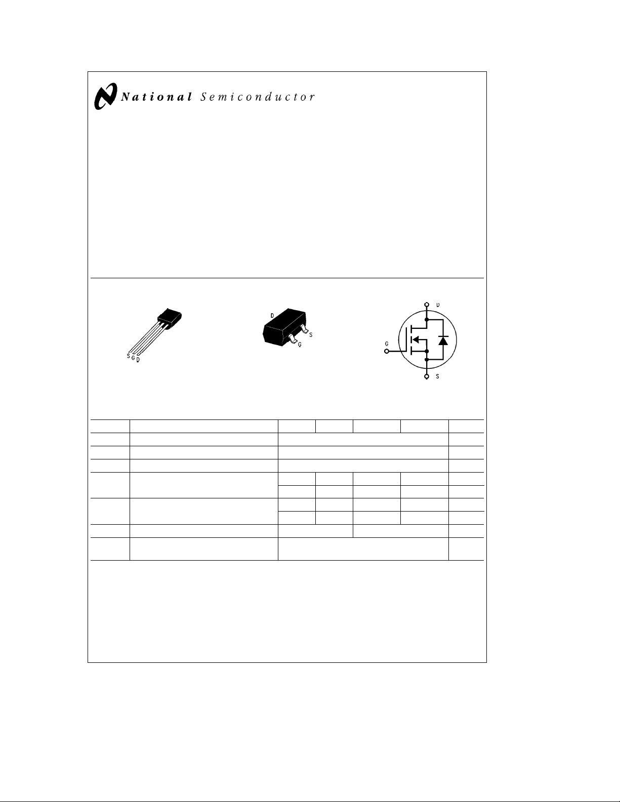
TL/G/11378– 2
TO-92
7000 Series
TL/G/11378– 1
TO-236 AB
(SOT-23)
TL/G/11378– 3
7002 Series
Absolute Maximum Ratings
Symbol Parameter 2N7000 2N7002 NDF7000A NDS7002A Units
V
DSS
V
DGR
V
GSS
I
D
P
D
TJ,T
T
L
Drain-Source Voltage 60 V
Drain-Gate Voltage (R
Gate-Source Voltage
s
1MX)60V
GS
g
40 V
Drain CurrentÐContinuous 200 115 400 280 mA
ÐPulsed 500 800 2000 1500 mA
Total Power Dissipation@T
e
25§C 400 200 625 300 mW
A
Derating above 25§C 3.2 1.6 5 2.4 mW/§C
Operating and Storage Temperature Range
STG
Maximum Lead Temperature for Soldering
Purposes, (/16* from Case for 10 Seconds
b
55 to 150
300
b
65 to 150
C
§
C
§
C
1995 National Semiconductor Corporation RRD-B30M115/Printed in U. S. A.
TL/G/11378
2N7000
e
T
Electrical Characteristics
Symbol Parameter Conditions Min Typ Max Units
OFF CHARACTERISTICS
BV
I
DSS
I
GSSF
ON CHARACTERISTICS*
V
GS(th)
r
DS(ON)
V
DS(ON)
I
D(ON)
g
FS
DYNAMIC CHARACTERISTICS
C
iss
C
oss
C
rss
SWITCHING CHARACTERISTICS*
t
on
t
off
BODY-DRAIN DIODE RATINGS
I
S
I
SM*
V
SD*
THERMAL CHARACTERISTICS
R
iJA
R
iJC
*Pulse Test: Pulse Widths300 ms, Duty Cycles2.0%.
Drain-Source Breakdown Voltage V
DSS
Zero Gate Voltage Drain Current V
Gate-Body Leakage, Forward V
Gate Threshold Voltage V
Static Drain-Source V
On-Resistance
Drain-Source On-Voltage V
On-State Drain Current V
Forward Transconductance V
Input Capacitance V
Output Capacitance 11 25 pF
Reverse Transfer Capacitance 4 5 pF
Turn-On Time V
Turn-Off Time
Maximum Continuous Drain-Source Diode Forward Current 200 mA
Maximum Pulsed Drain-Source Diode Forward Current 500 mA
Drain-Source Diode Forward Voltage V
Thermal Resistance, Junction to Ambient 312.5§C/W
Thermal Resistance, Junction to Case 40
25§C unless otherwise noted
C
e
0V, I
GS
DS
GS
DS
GS
GS
V
GS
GS
DS
DS
DD
R
G
GS
e
eb
e
e
e
e
e
e
e
e
e
e
48V, V
15V, V
VGS,I
10V, I
10V, I
4.5V, I
4.5V, V
10V, I
25V, V
15V, I
25X,R
0V, I
D
S
e
10 mA60 V
e
0V 1 mA
GS
e
T
125§C1mA
C
e
0V
DS
e
1 mA 0.8 2.1 3 V
D
e
0.5A 1.2 5 X
D
e
125§C 1.9 9 X
T
C
e
0.5A 0.6 2.5 V
D
e
75 mA 0.14 0.4 V
D
e
10V 75 600 mA
DS
e
200 mA 100 320 ms
D
e
0V, fe1.0 MHz 20 60 pF
GS
e
0.5V, V
D
e
25X
L
e
200 mA 1.5 V
e
10V, 10 ns
GS
b
10 nA
10 ns
C/W
§
2
2N7002
e
T
Electrical Characteristics
Symbol Parameter Conditions Min Typ Max Units
OFF CHARACTERISTICS
BV
I
DSS
I
GSSF
I
GSSR
ON CHARACTERISTICS*
V
GS(th)
r
DS(ON)
V
DS(ON)
I
D(ON)
g
FS
DYNAMIC CHARACTERISTICS
C
iss
C
oss
C
rss
SWITCHING CHARACTERISTICS*
t
ON
t
OFF
BODY-DRAIN DIODE RATINGS
I
S
I
SM
VSD* Drain-Source Diode Forward Voltage V
THERMAL CHARACTERISTICS
R
iJA
*Pulse Test: Pulse Widths300 ms, Duty Cycles2.0%.
Drain-Source Breakdown Voltage V
DSS
Zero Gate Voltage Drain Current V
Gate-Body Leakage, Forward V
Gate-Body Leakage, Reverse V
Gate Threshold Voltage V
Static Drain-Source V
On-Resistance
Drain-Source On-Voltage V
On-State Drain Current V
Forward Transconductance V
Input Capacitance V
Output Capacitance 11 25 pF
Reverse Transfer Capacitance 4 5 pF
Turn-On Time V
Turn-Off Time
Maximum Continuous Drain-Source Diode Forward Current 115 mA
Maximum Pulsed Drain-Source Diode Forward Current 800 mA
Thermal Resistance, Junction to Ambient 625§C/W
25§C unless otherwise noted
C
e
e
0V, I
GS
DS
GS
GS
DS
GS
V
GS
GS
V
GS
GS
DS
DS
DD
R
GEN
GS
D
e
60V, V
GS
e
20V 100 nA
eb
20V
e
VGS,I
D
e
10V, I
D
e
e
5V, I
D
e
10V, I
D
e
e
5V, I
D
e
10V, V
DS
t
2V
DS(ON),ID
e
25V, V
GS
e
30V, I
D
e
25X,R
e
e
0V, I
S
10 mA60V
e
0V 1 mA
e
T
125§C 500 mA
C
b
100 nA
e
250 mA 1 2.1 2.5 V
e
0.5A 1.2 7.5 X
e
T
125§C 2 13.5 X
C
50 mA 1.7 7.5 X
e
T
125§C 2.8 13.5 X
C
e
0.5A 0.6 3.75 V
50 mA 0.09 1.5 V
t
2V
DS(ON)
e
200 mA 80 320 ms
e
0V, fe1.0 MHz 20 50 pF
e
200 mA, V
e
L
150X
e
10V, 20 ns
GS
500 2700 mA
20 ns
115 mA 1.5 V
3
NDF7000A
e
T
Electrical Characteristics
Symbol Parameter Conditions Min Typ Max Units
OFF CHARACTERISTICS
BV
I
DSS
I
GSSF
ON CHARACTERISTICS*
V
GS(th)
r
DS(ON)
V
DS(ON)
I
D(ON)
g
FS
DYNAMIC CHARACTERISTICS
C
iss
C
oss
C
rss
SWITCHING CHARACTERISTICS*
t
on
t
off
BODY-DRAIN DIODE RATINGS
I
S
I
SM
VSD* Drain-Source Diode Forward Voltage V
THERMAL CHARACTERISTICS
R
iJA
*Pulse Test: Pulse Widths300 ms, Duty Cycles2.0%.
Drain-Source Breakdown Voltage V
DSS
Zero Gate Voltage Drain Current V
Gate-Body Leakage, Forward V
Gate Threshold Voltage V
Static Drain-Source V
On-Resistance
Drain-Source On-Voltage V
On-State Drain Current V
Forward Transconductance V
Input Capacitance V
Output Capacitance 11 25 pF
Reverse Transfer Capacitance 4 5 pF
Turn-On Time V
Turn-Off Time
Maximum Continuous Drain-Source Diode Forward Current 400 mA
Maximum Pulsed Drain-Source Diode Forward Current 2000 mA
Thermal Resistance, Junction to Ambient 200§C/W
25§C unless otherwise noted
C
e
0V, I
GS
DS
GS
DS
GS
GS
V
GS
GS
DS
DS
DD
R
G
GS
e
eb
e
e
e
e
e
t
e
e
e
e
48V, V
15V
VGS,I
10V, I
10V, I
4.5V, I
4.5V, V
2V
DS(ON),ID
25V, V
15V, I
25X,R
0V, I
D
S
e
10 mA60 V
e
0V 1 mA
GS
e
T
125§C1mA
C
b
10 nA
e
1 mA 0.8 2.1 3 V
D
e
0.5A 1.2 2 X
D
e
125§C 2 3.5 X
T
C
e
500 mA 0.6 1 V
D
e
75 mA 0.14 0.225 V
D
t
2V
DS
DS(ON)
e
200 mA 100 320 ms
e
0V, fe1.0 MHz 20 60 pF
GS
e
500 mA, V
D
e
25X
L
e
400 mA 0.88 1.2 V
GS
e
400 600 mA
10V, 10 ns
10 ns
4
 Loading...