

National LMV931MF, LMV931MG, LMV932MM, LMV932MA, LMV934MA Schematics
...
LMV931 Single/LMV932 Dual/LMV934 Quad 1.8V, RRIO Operational Amplifiers
LMV931 Single/LMV932 Dual/
LMV934 Quad
1.8V, RRIO Operational Amplifiers
General Description
The LMV931/LMV932/LMV934 are low voltage, low power
operational amplifiers. LMV931/LMV932/LMV934 operate
from +1.8V to +5.5V supply voltages and have rail-to-rail input
and output. LMV931/LMV932/LMV934 input common mode
voltage extends 200mV beyond the supplies which enables
user enhanced functionality beyond the supply voltage range.
The output can swing rail-to-rail unloaded and within 105mV
from the rail with 600Ω load at 1.8V supply. The LMV931/
LMV932/LMV934 are optimized to work at 1.8V which make
them ideal for portable two-cell battery powered systems and
single cell Li-Ion systems.
LMV931/LMV932/LMV934 exhibit excellent speed-power ratio, achieving 1.4MHz gain bandwidth product at 1.8V supply
voltage with very low supply current. The LMV931/LMV932/
LMV934 are capable of driving a 600Ω load and up to 1000pF
capacitive load with minimal ringing. LMV931/LMV932/
LMV934 have a high DC gain of 101dB, making them suitable
for low frequency applications.
The single LMV931 is offered in space saving 5-Pin SC70 and
SOT23 packages. The dual LMV932 are in 8-Pin MSOP and
SOIC packages and the quad LMV934 are in 14-Pin TSSOP
and SOIC packages. These small packages are ideal solutions for area constrained PC boards and portable electronics
such as cellular phones and PDAs.
Features
(Typical 1.8V Supply Values; Unless Otherwise Noted)
Guaranteed 1.8V, 2.7V and 5V specifications
■
Output swing
■
w/600Ω load 80mV from rail
—
w/2kΩ load 30mV from rail
—
V
■
CM
Supply current (per channel)
■
Gain bandwidth product 1.4MHz
■
Maximum V
■
Ultra tiny packages
■
Temperature range −40°C to 125°C
■
Applications
Consumer communication
■
Consumer computing
■
PDAs
■
Audio pre-amp
■
Portable/battery-powered electronic equipment
■
Supply current monitoring
■
Battery monitoring
■
OS
October 13, 2010
200mV beyond rails
100μA
4.0mV
Typical Application
200326h0
© 2010 National Semiconductor Corporation 200326 www.national.com
Absolute Maximum Ratings (Note 1)
If Military/Aerospace specified devices are required,
please contact the National Semiconductor Sales Office/
Distributors for availability and specifications.
ESD Tolerance (Note 2)
Machine Model 200V
Human Body Model 2000V
Supply Voltage (V+–V −)
Differential Input Voltage ± Supply Voltage
Voltage at Input/Output Pins V++0.3V, V- -0.3V
Storage Temperature Range −65°C to 150°C
Junction Temperature (Note 4) 150°C
6V
For soldering specifications:
see product folder at www.national.com and
www.national.com/ms/MS/MS-SOLDERING.pdf
Operating Ratings (Note 1)
Supply Voltage Range 1.8V to 5.5V
Temperature Range −40°C to 125°C
Thermal Resistance (θJA)
5-Pin SC70 414°C/W
5-Pin SOT23 265°C/W
8-Pin MSOP 235°C/W
8-Pin SOIC 175°C/W
14-Pin TSSOP 155°C/W
14-Pin SOIC 127°C/W
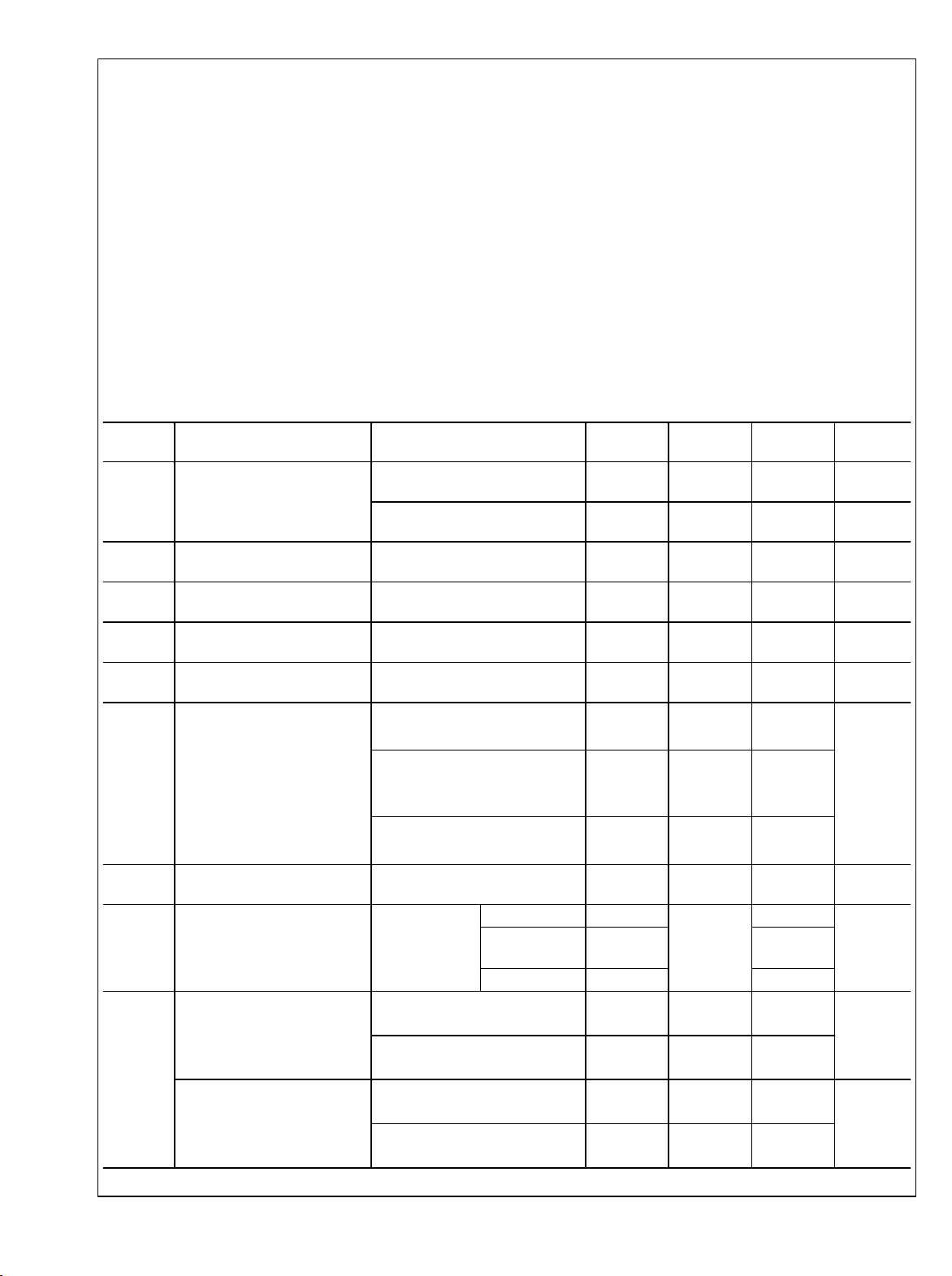
1.8V DC Electrical Characteristics
Unless otherwise specified, all limits guaranteed for TJ = 25°C. V+ = 1.8V, V − = 0V, VCM = V+/2, VO = V+/2 and
RL > 1 MΩ. Boldface limits apply at the temperature extremes. See (Note 10)
LMV931 Single/LMV932 Dual/LMV934 Quad
Symbol Parameter Condition Min
(Note 6)
V
OS
Input Offset Voltage LMV931 (Single) 1 4
LMV932 (Dual)
LMV934 (Quad)
TCV
Input Offset Voltage Average
OS
5.5
Drift
I
B
I
OS
I
S
CMRR Common Mode Rejection Ratio
Input Bias Current 15 35
Input Offset Current 13 25
Supply Current (per channel) 103 185
LMV931, 0 ≤ VCM ≤ 0.6V
1.4V ≤ VCM ≤ 1.8V (Note 8)
LMV932 and LMV934
0 ≤ VCM ≤ 0.6V
60
55
55
50
1.4V ≤ VCM ≤ 1.8V (Note 8)
−0.2V ≤ VCM ≤ 0V
50 72
1.8V ≤ VCM ≤ 2.0V
PSRR Power Supply Rejection Ratio
1.8V ≤ V+ ≤ 5V
75
70
CMVR Input Common-Mode Voltage
Range
For CMRR
Range ≥ 50dB
TA = 25°C V− −0.2 −0.2 to 2.1 V+ +0.2
TA −40°C to 85°
V
C
TA = 125°C V− +0.2 V+ −0.2
A
V
Large Signal Voltage Gain
LMV931 (Single)
Large Signal Voltage Gain
LMV932 (Dual)
LMV934 (Quad)
RL = 600Ω to 0.9V,
VO = 0.2V to 1.6V, VCM = 0.5V
RL = 2kΩ to 0.9V,
VO = 0.2V to 1.6V, VCM = 0.5V
RL = 600Ω to 0.9V,
VO = 0.2V to 1.6V, VCM = 0.5V
RL = 2kΩ to 0.9V,
VO = 0.2V to 1.6V, VCM = 0.5V
77
73
80
75
75
72
78
75
−
Typ
(Note 5)
100
101
105
100
Max
(Note 6)
1 5.5
205
78
76
90
6
7.5
50
40
V
Units
mV
mV
μV/°C
nA
nA
μA
dB
dB
+
V
dB
dB
www.national.com 2
LMV931 Single/LMV932 Dual/LMV934 Quad
Symbol Parameter Condition Min
(Note 6)
V
O
Output Swing
RL = 600Ω to 0.9V
VIN = ±100mV
1.65
1.63
Typ
(Note 5)
1.72
Max
(Note 6)
Units
0.077 0.105
RL = 2kΩ to 0.9V
VIN = ±100mV
1.75
1.74
0.120
1.77
V
0.024 0.035
0.04
I
O
Output Short Circuit Current
(Note 3)
Sourcing, VO = 0V
VIN = 100mV
Sinking, VO = 1.8V
VIN = −100mV
4
3.3
7
5
8
9
mA
1.8V AC Electrical Characteristics
Unless otherwise specified, all limits guaranteed for TJ = 25°C. V+ = 1.8V, V − = 0V, VCM = V+/2, VO = V+/2 and RL > 1 MΩ.
Boldface limits apply at the temperature extremes. See (Note 10)
Symbol Parameter Conditions Min
(Note 6)
SR Slew Rate (Note 7) 0.35
GBW Gain-Bandwidth Product 1.4 MHz
Φ
m
G
m
e
n
Phase Margin 67
Gain Margin 7
Input-Referred Voltage Noise f = 10 kHz, VCM = 0.5V 60
Typ
(Note 5)
Max
(Note 6)
Units
V/μs
deg
dB
i
n
THD Total Harmonic Distortion f = 1kHz, AV = +1
Input-Referred Current Noise f = 10 kHz 0.08
0.023
RL = 600Ω, VIN = 1 V
PP
%
Amp-to-Amp Isolation (Note 9) 123 dB
3 www.national.com

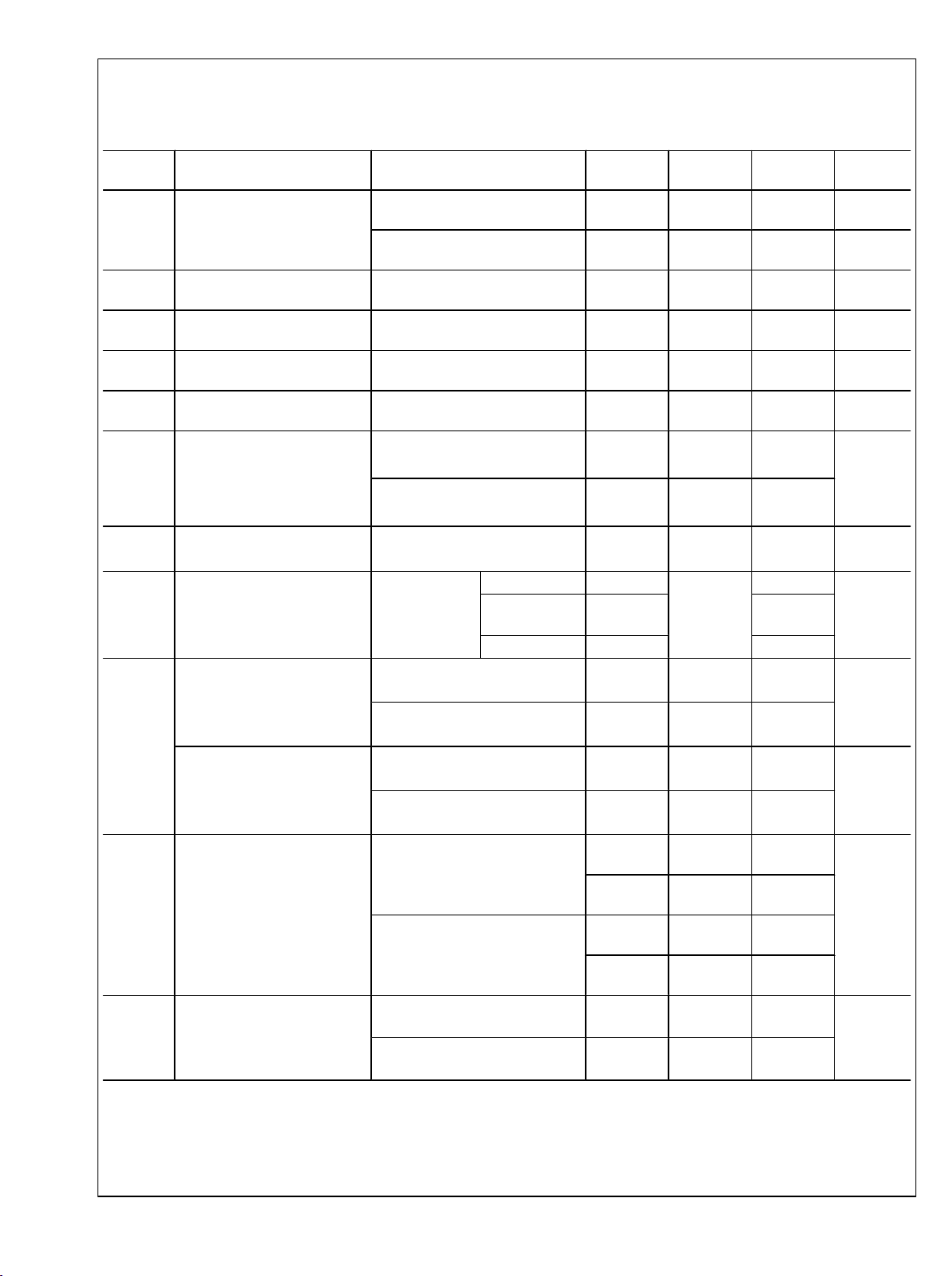
2.7V DC Electrical Characteristics
Unless otherwise specified, all limits guaranteed for TJ = 25°C. V+ = 2.7V, V − = 0V, VCM = V+/2, VO = V+/2 and
RL > 1 MΩ. Boldface limits apply at the temperature extremes. See (Note 10)
Symbol Parameter Condition Min
V
OS
Input Offset Voltage LMV931 (Single) 1 4
LMV932 (Dual)
LMV934 (Quad)
TCV
Input Offset Voltage Average
OS
5.5
Drift
I
B
I
OS
I
S
LMV931 Single/LMV932 Dual/LMV934 Quad
CMRR Common Mode Rejection Ratio
Input Bias Current 15 35
Input Offset Current 8 25
Supply Current (per channel) 105 190
LMV931, 0 ≤ VCM ≤ 1.5V
2.3V ≤ VCM ≤ 2.7V (Note 8)
LMV932 and LMV934
0 ≤ VCM ≤ 1.5V
2.3V ≤ VCM ≤ 2.7V (Note 8)
−0.2V ≤ VCM ≤ 0V
2.7V ≤ VCM ≤ 2.9V
PSRR Power Supply Rejection Ratio
1.8V ≤ V+ ≤ 5V
VCM = 0.5V
V
CM
Input Common-Mode Voltage
Range
For CMRR
Range ≥ 50dB
TA = 25°C V− −0.2 −0.2 to 3.0 V+ +0.2
TA = −40°C to
85°C
TA = 125°C V− +0.2 V+ −0.2
A
V
Large Signal Voltage Gain
LMV931 (Single)
RL = 600Ω to 1.35V,
VO = 0.2V to 2.5V
RL = 2kΩ to 1.35V,
VO = 0.2V to 2.5V
Large Signal Voltage Gain
LMV932 (Dual)
LMV934 (Quad)
RL = 600Ω to 1.35V,
VO = 0.2V to 2.5V
RL = 2kΩ to 1.35V,
VO = 0.2V to 2.5V
V
O
Output Swing
RL = 600Ω to 1.35V
VIN = ±100mV
RL = 2kΩ to 1.35V
VIN = ±100mV
I
O
Output Short Circuit Current
(Note 3)
Sourcing, VO = 0V
VIN = 100mV
Sinking, VO = 0V
VIN = −100mV
(Note 6)
1 5.5
60
55
55
50
50 74
75
70
−
V
87
86
92
91
78
75
81
78
2.55
2.53
0.083 0.110
2.65
2.64
0.025 0.04
20
15
18
12
Typ
(Note 5)
100
104
110
100
2.62
2.675
Max
(Note 6)
210
81
80
90
0.130
0.045
30
25
6
7.5
50
40
V
Units
mV
mV
μV/°C
nA
nA
μA
dB
dB
+
V
dB
dB
V
mA
www.national.com 4
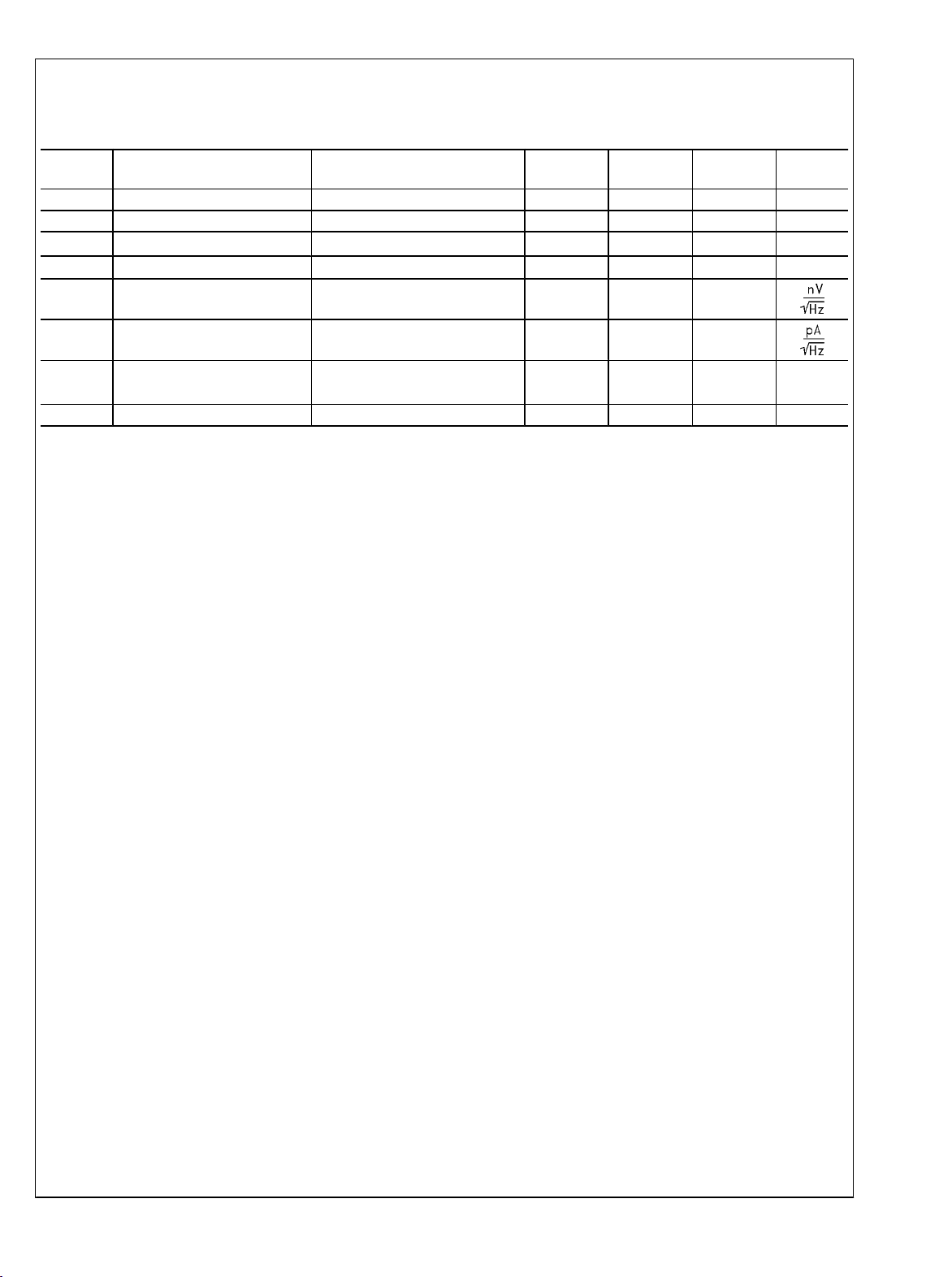
2.7V AC Electrical Characteristics
Unless otherwise specified, all limits guaranteed for TJ = 25°C. V+ = 2.7V, V − = 0V, VCM = 1.0V, VO = 1.35V and RL > 1 MΩ.
Boldface limits apply at the temperature extremes. See (Note 10)
Symbol Parameter Conditions Min
(Note 6)
SR Slew Rate (Note 7) 0.4 V/µs
GBW Gain-Bandwidth Product 1.4 MHz
Φ
m
G
m
e
n
Phase Margin 70
Gain Margin 7.5
Input-Referred Voltage Noise f = 10 kHz, VCM = 0.5V 57
Typ
(Note 5)
Max
(Note 6)
Units
deg
dB
LMV931 Single/LMV932 Dual/LMV934 Quad
i
n
THD Total Harmonic Distortion f = 1kHz, AV = +1
Input-Referred Current Noise f = 10 kHz 0.08
RL = 600Ω, VIN = 1V
PP
0.022 %
Amp-to-Amp Isolation (Note 9) 123 dB
5 www.national.com
5V DC Electrical Characteristics
Unless otherwise specified, all limits guaranteed for TJ = 25°C. V+ = 5V, V − = 0V, VCM = V+/2, VO = V+/2 and
RL > 1 MΩ. Boldface limits apply at the temperature extremes. See (Note 10)
Symbol Parameter Condition Min
V
OS
Input Offset Voltage LMV931 (Single) 1 4
LMV932 (Dual)
LMV934 (Quad)
TCV
Input Offset Voltage Average
OS
Drift
I
B
I
OS
I
S
LMV931 Single/LMV932 Dual/LMV934 Quad
CMRR Common Mode Rejection Ratio
Input Bias Current 14 35
Input Offset Current 9 25
Supply Current (per channel) 116 210
0 ≤ VCM ≤ 3.8V
4.6V ≤ VCM ≤ 5.0V (Note 8)
−0.2V ≤ VCM ≤ 0V
5.0V ≤ VCM ≤ 5.2V
PSRR Power Supply Rejection Ratio
1.8V ≤ V+ ≤ 5V
VCM = 0.5V
CMVR Input Common-Mode Voltage
Range
A
V
Large Signal Voltage Gain
LMV931 (Single)
For CMRR
Range ≥ 50dB
RL = 600Ω to 2.5V,
VO = 0.2V to 4.8V
RL = 2kΩ to 2.5V,
VO = 0.2V to 4.8V
Large Signal Voltage Gain
LMV932 (Dual)
LMV934 (Quad)
RL = 600Ω to 2.5V,
VO = 0.2V to 4.8V
RL = 2kΩ to 2.5V,
VO = 0.2V to 4.8V
V
O
Output Swing
RL = 600Ω to 2.5V
VIN = ±100mV
RL = 2kΩ to 2.5V
VIN = ±100mV
I
O
Output Short Circuit Current
(Note 3)
LMV931, Sourcing, VO = 0V
VIN = 100mV
Sinking, VO = 5V
VIN = −100mV
(Note 6)
1 5.5
5.5
60
55
50 78
75
70
TA = 25°C V− −0.2 −0.2 to 5.3 V+ +0.2
TA = −40°C to
−
V
85°C
TA = 125°C V− +0.3 V+ −0.3
88
87
94
93
81
78
85
82
4.855
4.835
0.120 0.160
4.945
4.935
0.037 0.065
80
68
58
45
(Note 5)
Typ
Max
(Note 6)
86
100
102
113
90
100
4.890
0.180
4.967
0.075
100
65
6
7.5
50
40
230
V
Units
mV
mV
μV/°C
nA
nA
μA
dB
dB
+
V
dB
dB
V
mA
www.national.com 6
 Loading...