

National LMV710M5, LMV711M6, LMV715MF Schematic [ru]
January 9, 2009
LMV710/LMV711/LMV715
Low Power, RRIO Operational Amplifiers with High Output
Current Drive and Shutdown Option
LMV710/LMV711/LMV715 Low Power, RRIO Operational Amplifiers with High Output Current
Drive and Shutdown Option
General Description
The LMV710/LMV711/LMV715 are BiCMOS operational amplifiers with a CMOS input stage. These devices have greater
than RR input common mode voltage range, rail-to-rail output
and high output current drive. They offer a bandwidth of 5 MHz
and a slew rate of 5 V/µs.
On the LMV711/LMV715, a separate shutdown pin can be
used to disable the device and reduces the supply current to
0.2 µA (typical). They also feature a turn on time of less than
10 µs. It is an ideal solution for power sensitive applications,
such as cellular phone, pager, palm computer, etc. In addition, once the LMV715 is in shutdown the output will be “Tristated”.
The LMV710 is offered in the space saving 5-Pin SOT23 Tiny
package. The LMV711/LMV715 are offered in the space saving 6-Pin SOT23 Tiny package.
The LMV710/LMV711/LMV715 are designed to meet the demands of low power, low cost, and small size required by
cellular phones and similar battery powered portable electronics.
Typical Application
Features
(For 5V supply, typical unless otherwise noted).
Low offset voltage 3 mV, max
■
Gain-bandwidth product 5 MHz, typ
■
Slew rate 5 V/µs, typ
■
Space saving packages 5-Pin and 6-Pin SOT23
■
Turn on time from shutdown <10 µs
■
Industrial temperature range −40°C to +85°C
■
Supply current in shutdown mode 0.2 µA, typ
■
Guaranteed 2.7V and 5V performance
■
Unity gain stable
■
Rail-to-rail input and output
■
Capable of driving 600Ω load
■
Applications
Wireless phones
■
GSM/TDMA/CDMA power amp control
■
AGC, RF power detector
■
Temperature compensation
■
Wireless LAN
■
Bluetooth
■
HomeRF
■
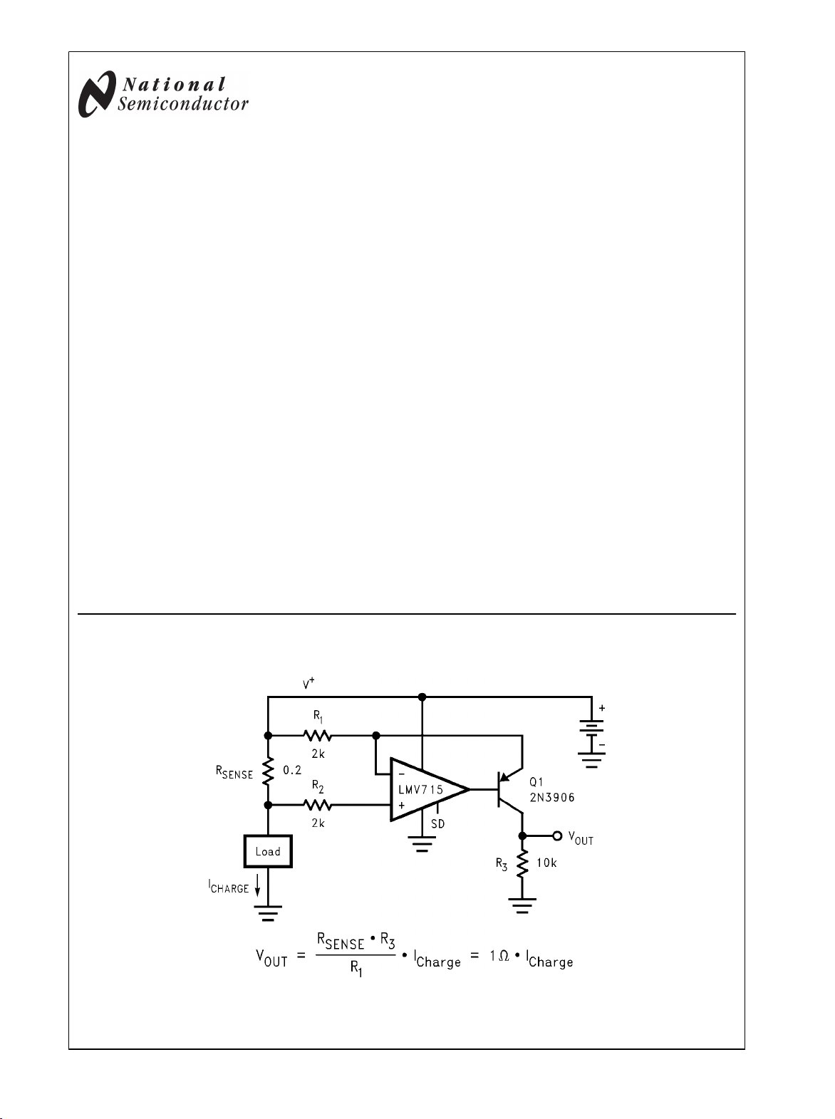
High Side Current Sensing
10132513
© 2009 National Semiconductor Corporation 101325 www.national.com
Absolute Maximum Ratings (Note 1)
If Military/Aerospace specified devices are required,
please contact the National Semiconductor Sales Office/
Distributors for availability and specifications.
ESD Tolerance (Note 2)
Machine Model 100V
Human Body Model 2000V
Differential Input Voltage ± Supply Voltage
Voltage at Input/Output Pin (V+) + 0.4V
LMV710/LMV711/LMV715
Supply Voltage (V+ - V −)
Output Short Circuit to V
Output Short Circuit to V
+
−
(V−) − 0.4V
5.5V
(Note 3)
(Note 4)
Current at Input Pin ± 10 mA
Mounting Temp.
Infrared or Convection (20 sec) 235°C
Storage Temperature Range −65°C to 150°C
Junction Temperature (T
JMAX
)
(Note 5)
Operating Ratings (Note 1)
Supply Voltage 2.7V to 5.0V
Temperature Range −40°C to 85°C
Thermal Resistance (θJA)
MF05A Package, 5-Pin SOT23 265 °C/W
MF06A package, 6-Pin SOT23 265 °C/W
2.7V Electrical Characteristics
Unless otherwise specified, all limits guaranteed for TJ = 25°C. V+ = 2.7V, V − = 0V, VCM = 1.35V and RL > 1 MΩ. Boldface limits
apply at the temperature extremes.
Symbol Parameter Condition Typ
(Note 6)
V
OS
I
B
CMRR Common Mode Rejection Ratio
PSRR Power Supply Rejection Ratio
Input Offset Voltage VCM = 0.85V and VCM = 1.85V 0.4 3
Input Bias Current 4 pA
0 ≤ VCM ≤ 2.7V
2.7V ≤ V+ ≤ 5V,
VCM = 0.85V
2.7V ≤ V+ ≤ 5V,
VCM = 1.85V
V
CM
I
SC
Input Common-Mode Voltage Range
For CMRR ≥ 50 dB
Output Short Circuit Current Sourcing
VO = 0V
Sinking
VO = 2.7V
V
O
Output Swing
RL = 10 kΩ to 1.35V
RL = 600Ω to 1.35V
VO (SD) Output Voltage Level in
50 200 mV
Shutdown Mode (LMV711 only)
IO (SD) Output Leakage Current in
1 pA
Shutdown Mode (LMV715 Only)
CO (SD) Output Capacitance in
32 pF
Shutdown Mode (LMV715 Only)
I
S
Supply Current On Mode 1.22 1.7
Shutdown Mode, VSD = 0V 0.002 10 µA
75 50
110 70
95 70
-0.3 -0.2
3 2.9
28 15
40 25
2.68 2.62
0.01 0.12
2.55 2.52
0.05 0.23
Limits
(Note 7)
3.2
45
68
68
12
22
2.60
0.15
2.50
0.30
1.9
150°C
Units
mV
max
dB
min
dB
min
dB
min
V
mA
min
mA
min
V
min
V
max
V
min
V
max
mA
max
www.national.com 2
LMV710/LMV711/LMV715
Symbol Parameter Condition Typ
(Note 6)
A
V
Large Signal Voltage Sourcing
RL = 10 kΩ
115 80
Limits
(Note 7)
76
Units
dB
min
VO = 1.35V to 2.3V
Sinking
RL = 10 kΩ
113 80
76
dB
min
VO = 0.4V to 1.35V
Sourcing
RL = 600Ω
110 80
76
dB
min
VO = 1.35V to 2.2V
Sinking
RL = 600Ω
100 80
76
dB
min
VO = 0.5V to 1.35V
SR Slew Rate (Note 8) 5 V/µs
GBWP Gain-Bandwidth Product 5 MHz
φ
m
T
ON
V
SD
Phase Margin 60 Deg
Turn-on Time from Shutdown <10 µs
Shutdown Pin Voltage Range On Mode 1.5 to 2.7 2.4 to 2.7 V
Shutdown Mode 0 to 1 0 to 0.8 V
e
n
Input-Referred Voltage Noise f = 1 kHz 20
3.2V Electrical Characteristics
Unless otherwise specified, all limits guaranteed for TJ = 25°C. V+ = 3.2V, V− = 0V, VCM = 1.6V. Boldface limits apply at the
temperature extremes.
Symbol Parameter Conditions Typ
(Note 6)
V
O
Output Swing IO = 6.5 mA 3.0 2.95
Limit
(Note 7)
2.92
0.01 0.18
0.25
5V Electrical Characteristics
Unless otherwise specified, all limits guaranteed for TJ = 25°C. V+ = 5V, V − = 0V, VCM = 2.5V, and RL > 1 MΩ. Boldface limits
apply at the temperature extremes.
Symbol Parameter Condition Typ
(Note 6)
V
OS
I
B
CMRR Common Mode Rejection Ratio
PSRR Power Supply Rejection Ratio
Input Offset Voltage VCM = 0.85V and VCM = 1.85V 0.4 3
Input Bias Current 4 pA
0V ≤ VCM ≤ 5V
2.7V ≤ V+ ≤ 5V,
VCM = 0.85V
2.7V ≤ V+ ≤ 5V,
VCM = 1.85V
V
CM
Input Common-Mode Voltage Range
For CMRR ≥ 50 dB
70 50
110 70
95 70
-0.3 −0.2
5.3 5.2
Limits
(Note 7)
3.2
48
68
68
Units
V
min
V
max
Units
mV
max
dB
min
dB
min
dB
min
V
3 www.national.com
Symbol Parameter Condition Typ
(Note 6)
I
SC
Output Short Circuit Current Sourcing
VO = 0V
Sinking
VO = 5V
V
O
Output Swing
RL = 10 kΩ to 2.5V
35 25
40 25
4.98 4.92
Limits
(Note 7)
21
21
4.90
0.01 0.12
LMV710/LMV711/LMV715
RL = 600Ω to 2.5V
4.85 4.82
0.15
4.80
0.05 0.23
0.3
VO (SD) Output Voltage Level in
50 200 mV
Shutdown Mode (LMV711 only)
IO (SD) Output Leakage Current in
1 pA
Shutdown Mode (LMV715 Only)
CO (SD) Output Capacitance in
32 pF
shutdown Mode (LMV715 Only)
I
S
Supply Current On Mode 1.17 1.7
1.9
Shutdown Mode 0.2 10 µA
A
V
Large Signal Voltage Gain Sourcing
RL = 10 kΩ
123 80
76
VO = 2.5V to 4.6V
Sinking
RL = 10 kΩ
120 80
76
VO = 0.4V to 2.5V
Sourcing
RL = 600Ω
110 80
76
VO = 2.5V to 4.5V
Sinking
RL = 600Ω
118 80
76
VO = 0.5V to 2.5V
SR Slew Rate (Note 8) 5 V/µs
GBWP Gain-Bandwidth Product 5 MHz
φ
m
T
ON
V
SD
Phase Margin 60 Deg
Turn-on Time from Shutdown <10 µs
Shutdown Pin Voltage Range On Mode 2 to 5 2.4 to 5
Shutdown Mode 0 to 1.5 0 to 0.8
e
n
Input-Referred Voltage Noise f = 1 kHz 20
Units
mA
min
mA
min
V
min
V
max
V
min
V
max
mA
max
dB
min
dB
min
dB
min
dB
min
V
Note 1: Absolute Maximum Ratings indicate limits beyond which damage to the device may occur. Operating Ratings indicate conditions for which the device is
intended to be functional, but specific performance is not guaranteed. For guaranteed specifications and the test conditions, see the Electrical Characteristics.
Note 2: Human body model, 1.5 kΩ in series with 100 pF. Machine model, 0Ω in series with 100 pF.
Note 3: Shorting circuit output to V+ will adversely affect reliability.
Note 4: Shorting circuit output to V− will adversely affect reliability.
Note 5: The maximum power dissipation is a function of T
PD = (T
Note 6: Typical values represent the most likely parametric norm.
Note 7: All limits are guaranteed by testing or statistical analysis.
Note 8: Number specified is the slower of the positive and negative slew rates.
www.national.com 4
- T A)/θJA. All numbers apply for packages soldered directly into a PC board.
J(MAX)
, θJA, and TA. The maximum allowable power dissipation at any ambient temperature is
J(MAX)
LMV710/LMV711/LMV715
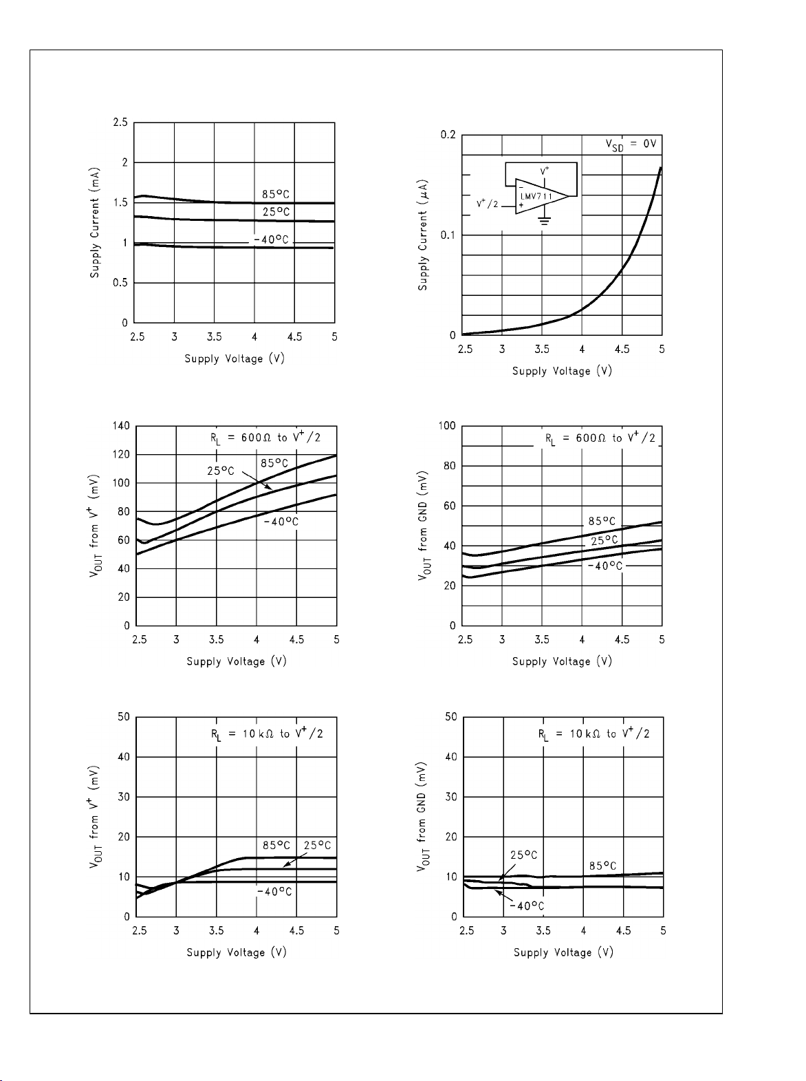
Typical Performance Characteristics Unless otherwise specified, V
Supply Current vs. Supply Voltage (On Mode)
10132527
Output Positive Swing vs. Supply Voltage
LMV711/LMV715 Supply Current vs.
Supply Voltage (Shutdown Mode)
Output Negative Swing vs. Supply Voltage
= +5V, single supply, TA = 25°C.
S
10132528
10132529
Output Positive Swing vs. Supply Voltage
10132531
10132530
Output Negative Swing vs. Supply Voltage
10132532
5 www.national.com
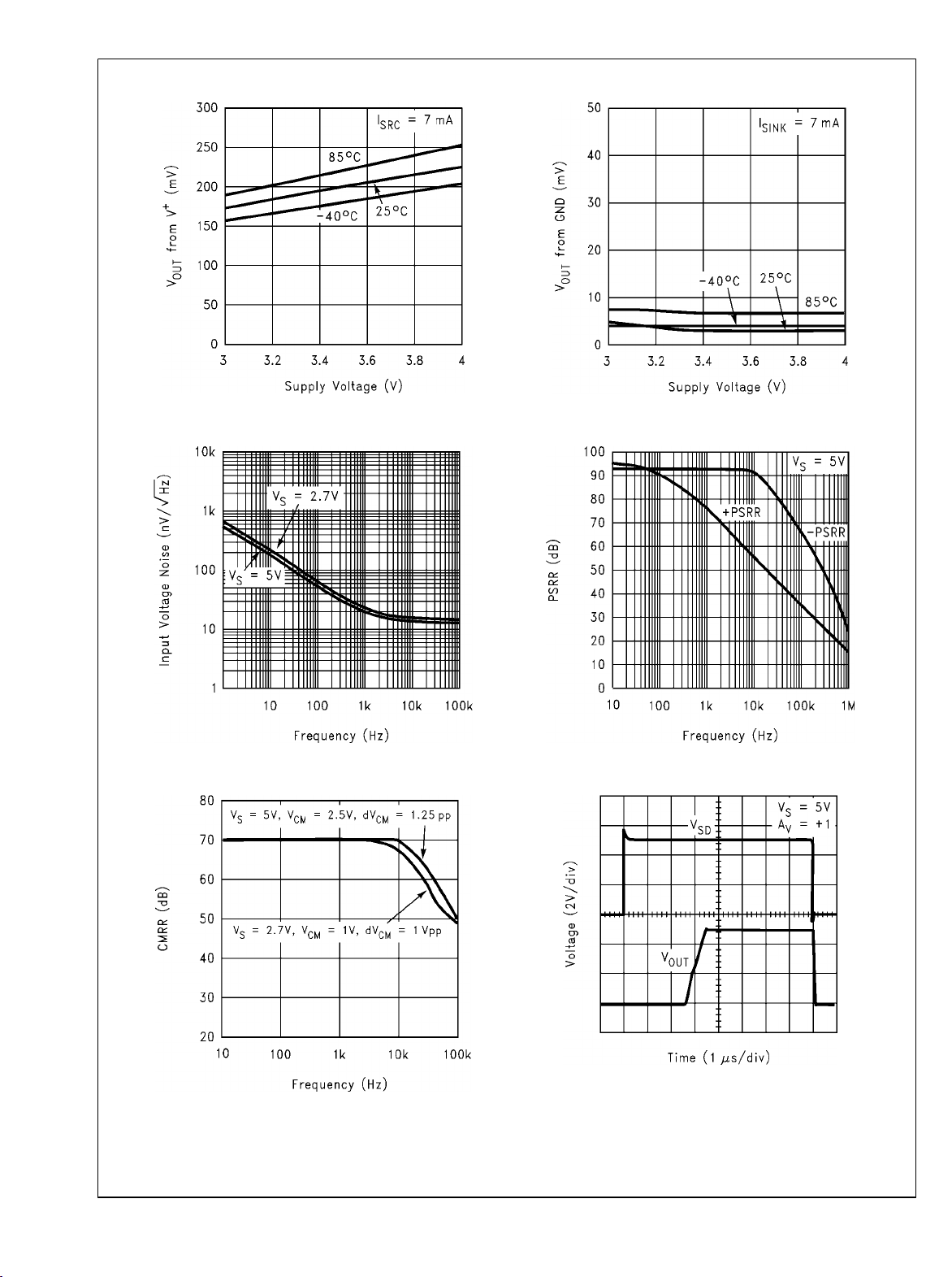
Output Positive Swing vs. Supply Voltage
LMV710/LMV711/LMV715
Output Negative Swing vs. Supply Voltage
Input Voltage Noise vs. Frequency
CMRR vs. Frequency
10132533
10132535
10132534
PSRR vs. Frequency
10132536
LMV711/LMV715 Turn On Characteristics
10132537
www.national.com 6
10132538
 Loading...