

National LMV341MG, LMV342MM, LMV342MA, LMV344MA, LMV344MT Schematic [ru]
January 25, 2008
LMV341/LMV342/LMV344
Single with Shutdown/Dual/Quad General Purpose, 2.7V,
Rail-to-Rail Output, 125°C, Operational Amplifiers
General Description
The LMV341/LMV342/LMV344 are single, dual, and quad low
voltage, low power Operational Amplifiers. They are designed
specifically for low voltage portable applications. Other important product characteristics are low input bias current, railto-rail output, and wide temperature range.
The patented class AB turnaround stage significantly reduces
the noise at higher frequencies, power consumption, and offset voltage. The PMOS input stage provides the user with
ultra-low input bias current of 20fA (typical) and high input
impedance.
The industrial-plus temperature range of −40°C to 125°C allows the LMV341/LMV342/LMV344 to accommodate a broad
range of extended environment applications. LMV341 expands National Semiconductor's Silicon Dust™ amplifier portfolio offering enhancements in size, speed, and power
savings. The LMV341/LMV342/LMV344 are guaranteed to
operate over the voltage range of 2.7V to 5.5V and all have
rail-to-rail output.
The LMV341 offers a shutdown pin that can be used to disable
the device. Once in shutdown mode, the supply current is reduced to 45pA (typical). The LMV341/LMV342/LMV344 have
29nV Voltage Noise at 10KHz, 1MHz GBW, 1.0V/μs Slew
Rate, 0.25mVos, and 0.1μA shutdown current (LMV341.)
The LMV341 is offered in the tiny 6-Pin SC70 package, the
LMV342 in space saving 8-Pin MSOP and SOIC, and the
LMV344 in 14-Pin TSSOP and SOIC. These small package
amplifiers offer an ideal solution for applications requiring
minimum PC board footprint. Applications with area con-
strained PC board requirements include portable electronics
such as cellular handsets and PDAs.
Features
(Typical 2.7V supply values; unless otherwise noted)
Guaranteed 2.7V and 5V specifications
■
Input referred voltage noise (@ 10kHz) 29nV/√Hz
■
Supply current (per amplifier)
■
Gain bandwidth product 1.0MHz
■
Slew rate 1.0V/μs
■
Shutdown Current (LMV341) 45pA
■
Turn-on time from shutdown (LMV341)
■
Input bias current 20fA
■
100μA
Applications
Cordless/cellular phones
■
Laptops
■
PDAs
■
PCMCIA/Audio
■
Portable/battery-powered electronic equipment
■
Supply current monitoring
■
Battery monitoring
■
Buffer
■
Filter
■
Driver
■
LMV341/LMV342/LMV344 Single with Shutdown/Dual/Quad General Purpose, 2.7V, Rail-to-Rail
Output, 125°C, Operational Amplifiers
5μs
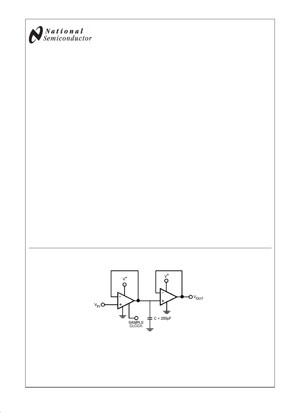
Sample and Hold Circuit
20030444
Silicon Dust™ is a trademark of National Semiconductor Corporation.
© 2008 National Semiconductor Corporation 200304 www.national.com
Absolute Maximum Ratings (Note 1)
If Military/Aerospace specified devices are required,
please contact the National Semiconductor Sales Office/
Distributors for availability and specifications.
ESD Tolerance (Note 2)
Machine Model 200V
Human Body Model 2000V
Differential Input Voltage ± Supply Voltage
Supply Voltage (V + -V −)
LMV341/LMV342/LMV344
Output Short Circuit to V
Output Short Circuit to V
Storage Temperature Range −65°C to 150°C
Junction Temperature (Note 5) 150°C
Mounting Temperature
+
−
6.0V
(Note 3)
(Note 4)
Infrared or Convection Reflow
(20 sec.) 235°C
Wave Soldering Lead Temp.
(10 sec.) 260°C
Operating Ratings (Note 1)
Supply Voltage 2.7V to 5.5V
Temperature Range −40°C to 125°C
Thermal Resistance (θ
6-Pin SC70 414°C/W
8-Pin SOIC 190°C/W
8-Pin MSOP 235°C/W
14-Pin TSSOP 155°C/W
14-Pin SOIC 145°C/W
JA
)
2.7V DC Electrical Characteristics (Note 10)
Unless otherwise specified, all limits guaranteed for TJ = 25°C, V+ = 2.7V, V− = 0V, VCM = V+/2, VO = V+/2 and RL > 1MΩ. Boldface
limits apply at the temperature extremes.
Symbol Parameter Conditions Min
(Note 7)
V
OS
Input Offset Voltage LMV341 0.25 4
LMV342/LMV344 0.55 5
TCV
Input Offset Voltage Average
OS
1.7 µV/°C
Drift
I
B
I
OS
I
S
Input Bias Current 0.02 120
Input Offset Current 6.6 fA
Supply Current Per Amplifier 100 170
Shutdown Mode, VSD = 0V
45pA
(LMV341)
CMRR Common Mode Rejection Ratio
0V ≤ VCM ≤ 1.7V
0V ≤ VCM ≤ 1.6V
PSRR Power Supply Rejection Ratio
V
CM
A
V
Input Common Mode Voltage
Large Signal Voltage Gain
2.7V ≤ V+ ≤ 5V
For CMRR ≥ 50dB
RL = 10kΩ to 1.35V
RL = 2kΩ to 1.35V
V
O
Output Swing
RL = 2kΩ to 1.35V
RL = 10kΩ to 1.35V
24 60
5.0 30
56
50
65
60
0 −0.2 to 1.9
78
70
72
64
60
95
30
40
Typ
(Note 6)
Max
(Note 7)
4.5
5.5
250
230
1μA
1.5μA
80 dB
82 dB
1.7 V
(Range)
113
103
95
26
40
5.3
Units
mV
pA
μA
dB
mV
www.national.com 2
LMV341/LMV342/LMV344
Symbol Parameter Conditions Min
(Note 7)
I
O
Output Short Circuit Current Sourcing
20 32
Typ
(Note 6)
Max
(Note 7)
LMV341/LMV342
18 24
LMV344
Sinking 15 24
t
on
V
SD
Turn-on Time from Shutdown (LMV341) 5
Shutdown Pin Voltage Range ON Mode (LMV341) 1.7 to 2.7 2.4 to 2.7
Shutdown Mode (LMV341) 0 to 1 0 to 0.8
2.7V AC Electrical Characteristics (Note 10)
Unless otherwise specified, all limits guaranteed for TJ = 25°C, V+ = 2.7V, V− = 0V, VCM = V+/2, VO = V+/2 and RL > 1MΩ.
Boldface limits apply at the temperature extremes.
Symbol Parameter Conditions Min
(Note 7)
SR Slew Rate
GBW Gain Bandwidth Product
Φ
m
G
m
e
n
i
n
Phase Margin
Gain Margin
Input-Referred Voltage Noise f = 1kHz 40
Input-Referred Current Noise f = 1kHz 0.001
RL = 10kΩ, (Note 9)
RL = 100kΩ, CL = 200pF
RL = 100kΩ
RL = 100kΩ
THD Total Harmonic Distortion f = 1kHz, AV = +1
RL = 600Ω, VIN = 1V
PP
1.0
1.0 MHz
72 deg
20 dB
0.017 %
Typ
(Note 6)
Max
(Note 7)
Units
mASourcing
μs
V
Units
V/μs
nV/
pA/
5V DC Electrical Characteristics (Note 10)
Unless otherwise specified, all limits guaranteed for TJ = 25°C, V+ = 5V, V− = 0V, VCM = V+/2, VO = V+/2 and R L > 1MΩ. Bold-
face limits apply at the temperature extremes.
Symbol Parameter Conditions Min
(Note 7)
V
OS
Input Offset Voltage LMV341 0.025 4
LMV342/LMV344 0.70 5
TCV
Input Offset Voltage Average
OS
1.9 µV/°C
Drift
I
B
I
OS
I
S
Input Bias Current 0.02 200
Input Offset Current 6.6 fA
Supply Current Per Amplifier 107 200
Shutdown Mode, VSD = 0V
0.033 1
(LMV341)
CMRR Common Mode Rejection Ratio
0V ≤ VCM ≤ 4.0V
0V ≤ VCM ≤ 3.9V
PSRR Power Supply Rejection Ratio
V
CM
Input Common Mode Voltage
2.7V ≤ V+ ≤ 5V
For CMRR ≥ 50dB
56
50
65
60
0 −0.2 to 4.2
Typ
(Note 6)
Max
(Note 7)
4.5
5.5
375
260
1.5
86 dB
82 dB
4 V
(Range)
Units
mV
pA
μA
μA
3 www.national.com
Symbol Parameter Conditions Min
(Note 7)
A
V
Large Signal Voltage Gain (Note
RL = 10kΩ to 2.5V
8)
RL = 2kΩ to 2.5V
78
70
72
Typ
(Note 6)
116
107
Max
(Note 7)
64
V
O
Output Swing
RL = 2kΩ to 2.5V
32 60
95
LMV341/LMV342/LMV344
RL = 10kΩ to 2.5V
60
95
7 30
34
40
30
7
40
I
O
Output Short Circuit Current Sourcing 85 113
Sinking 50 75
t
on
V
SD
Turn-on Time from Shutdown (LMV341) 5 µs
Shutdown Pin Voltage Range ON Mode (LMV341) 3.1 to 5 4.5 to 5.0
Shutdown Mode (LMV341) 0 to 1 0 to 0.8
5V AC Electrical Characteristics (Note 10)
Unless otherwise specified, all limits guaranteed for TJ = 25°C, V+ = 5V, V− = 0V, VCM = V+/2, VO = V+/2 and R L > 1MΩ. Bold-
face limits apply at the temperature extremes.
Symbol Parameter Conditions Min
(Note 7)
SR Slew Rate
GBW Gain-Bandwidth Product
Φ
m
G
m
e
n
i
n
Phase Margin
Gain Margin
Input-Referred Voltage Noise f = 1kHz 39
Input-Referred Current Noise f = 1kHz 0.001
RL = 10kΩ, (Note 9)
RL = 10kΩ, CL = 200pF
RL = 100kΩ
RL = 100kΩ
THD Total Harmonic Distortion f = 1kHz, AV = +1
RL = 600Ω, VIN = 1V
PP
1.0 V/µs
1.0 MHz
70 deg
20 dB
0.012 %
Typ
(Note 6)
Max
(Note 7)
Units
dB
mV
mV
mA
V
Units
nV/
pA/
Note 1: Absolute Maximum Ratings indicate limits beyond which damage to the device may occur. Operating Ratings indicate conditions for which the device is
intended to be functional, but specific performance is not guaranteed. For guaranteed specifications and the test conditions, see the Electrical Characteristics.
Note 2: Human Body Model, applicable std. MIL-STD-883, Method 3015.7. Machine Model, applicable std. JESD22-A115-A (ESD MM std. of JEDEC)
Field-Induced Charge-Device Model, applicable std. JESD22-C101-C (ESD FICDM std. of JEDEC).
Note 3: Shorting output to V+ will adversely affect reliability.
Note 4: Shorting output to V- will adversely affect reliability.
Note 5: The maximum power dissipation is a function of T
is PD = (T
Note 6: Typical values represent the most likely parametric norm as determined at the time of characterization. Actual typical values may vary over time and will
also depend on the application and configuration. The typical values are not tested and are not guaranteed on shipped production material.
Note 7: All limits are guaranteed by testing or statistical analysis.
Note 8: RL is connected to mid-supply. The output voltage is GND + 0.2V ≤ VO ≤ V+ −0.2V
Note 9: Connected as voltage follower with 2VPP step input. Number specified is the slower of the positive and negative slew rates.
Note 10: Electrical Table values apply only for factory testing conditions at the temperature indicated. Factory testing conditions result in very limited self-heating
of the device such that TJ = TA. No guarantee of parametric performance is indicated in the electrical tables under conditions of internal self heating where TJ >
TA.
www.national.com 4
– TA)/ θJA. All numbers apply for packages soldered directly onto a PC Board.
J(MAX)
, θJA. The maximum allowable power dissipation at any ambient temperature
J(MAX)
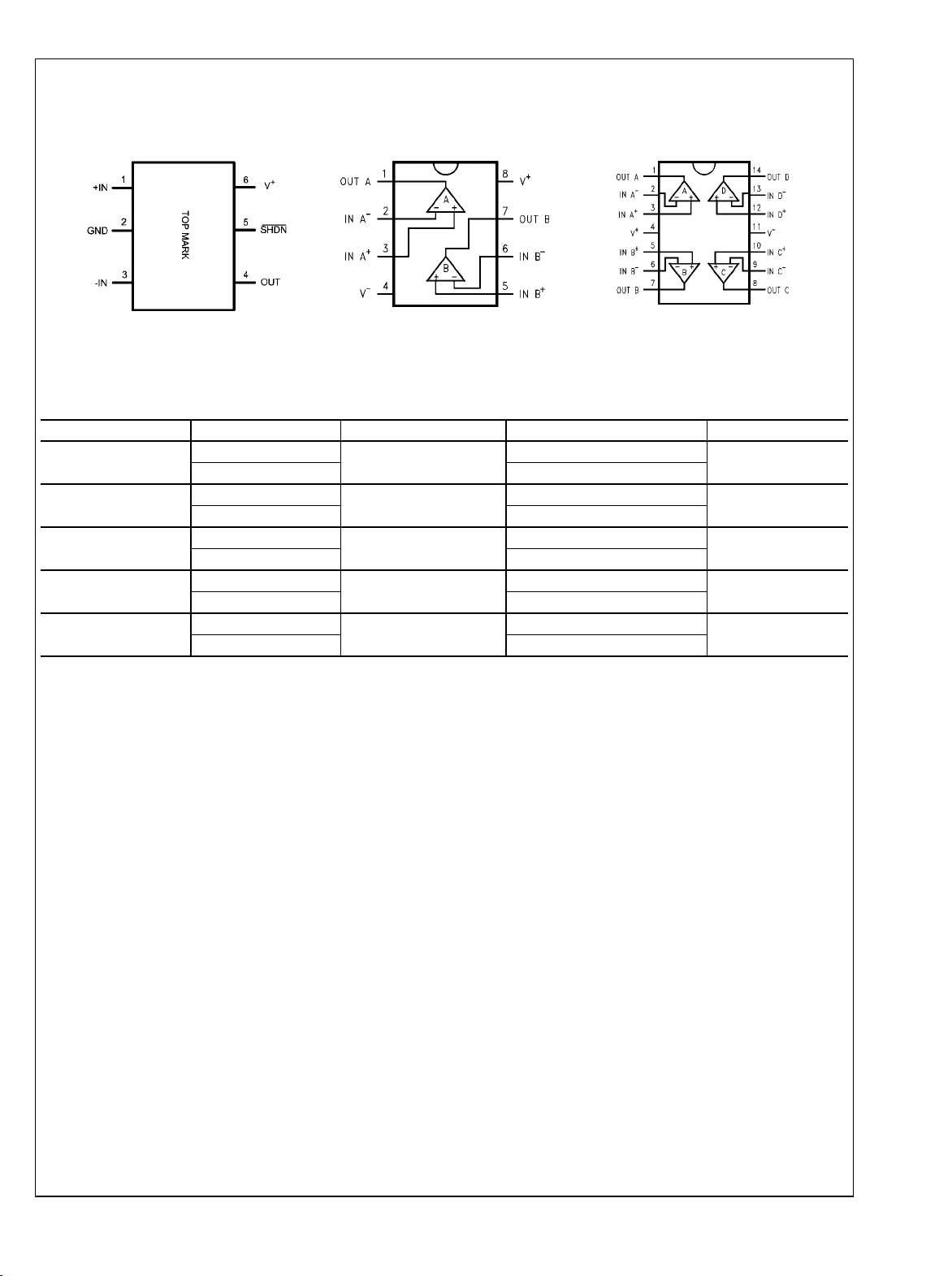
Connection Diagrams
LMV341/LMV342/LMV344
6-Pin SC70
Top View
20030441
8-Pin MSOP/SOIC
Top View
20030451
14-Pin TSSOP/SOIC
Top View
Ordering Information
Package Part Number Package Marking Transport Media NSC Drawing
6-Pin SC70
8-Pin MSOP
8-Pin SOIC
14-Pin TSSOP
14-Pin SOIC
LMV341MG
LMV341MGX 3k Units Tape and Reel
LMV342MM
LMV342MMX 3.5k Units Tape and Reel
LMV342MA
LMV342MAX 2.5k Units Tape and Reel
LMV344MT
LMV344MTX 2.5k Units Tape and Reel
LMV344MA
LMV344MAX 2.5k Units Tape and Reel
A78
A82A
LMV342MA
LMV344MT
LMV344MA
1k Units Tape and Reel
1k Units Tape and Reel
95 Units/Rail
Rails
55 Units/Rail
20030452
MAA06A
MUA08A
M08A
MTC14
M14A
5 www.national.com
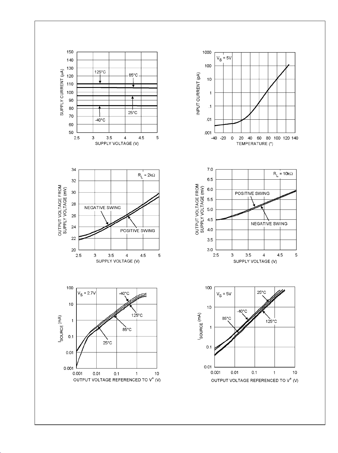
Typical Performance Characteristics
Supply Current vs. Supply Voltage (LMV341)
LMV341/LMV342/LMV344
Output Voltage Swing vs. Supply Voltage
20030428
Input Current vs. Temperature
20030446
Output Voltage Swing vs. Supply Voltage
20030426
I
vs. V
SOURCE
www.national.com 6
OUT
20030429
I
SOURCE
vs. V
20030427
OUT
20030430
 Loading...