


National LM8261M5 Schematic [ru]
LM8261 Single
RRIO, High Output Current & Unlimited Cap Load Op
Amp in SOT23-5
General Description
The LM8261 is a Rail-to-Rail input and output Op Amp which
can operate with a wide supply voltage range. This device
has high output current drive, greater than Rail-to-Rail input
common mode voltage range, unlimited capacitive load drive
capability, and provides tested and guaranteed high speed
and slew rate while requiring only 0.97mA supply current. It
is specifically designed to handle the requirements of flat
panel TFT panel V
suitable for other low power, and medium speed applications
which require ease of use and enhanced performance over
existing devices.
Greater than Rail-to-Rail input common mode voltage range
with 50dB of Common Mode Rejection, allows high side and
low side sensing, among many applications, without having
any concerns over exceeding the range and no compromise
in accuracy. Exceptionally wide operating supply voltage
range of 2.5V to 30V alleviates any concerns over functionality under extreme conditions and offers flexibility of use in
multitude of applications. In addition, most device parameters are insensitive to power supply variations; this design
enhancement is yet another step in simplifying its usage.
The output stage has low distortion (0.05% THD+N) and can
supply a respectable amount of current (15mA) with minimal
headroom from either rail (300mV).
driver applications as well as being
COM
The LM8261 is offered in the space saving SOT23-5 package.
Features
(VS=5V,TA= 25˚C, Typical values unless specified).
n GBWP 21MHz
n Wide supply voltage range 2.5V to 30V
n Slew rate 12V/µs
n Supply current 0.97 mA
n Cap load limit Unlimited
n Output short circuit current +53mA/−75mA
±
n
5% Settling time 400ns (500pF, 100mVPPstep)
n Input common mode voltage 0.3V beyond rails
n Input voltage noise 15nV/
n Input current noise 1pA/
n THD+N
Applications
n TFT-LCD flat panel V
n A/D converter buffer
n High side/low side sensing
n Headphone amplifier
COM
driver
April 2006
<
0.05%
LM8261 Single RRIO, High Output Current & Unlimited Cap Load Op Amp in SOT23-5
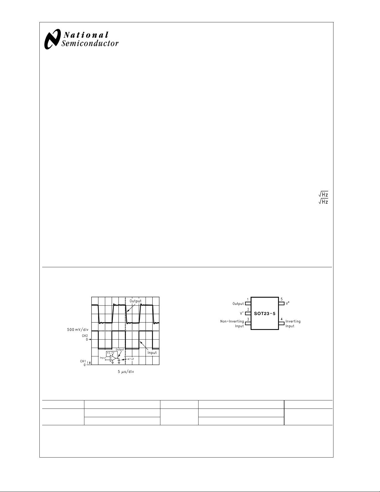
Output Response with Heavy Capacitive Load
10108437
Connection Diagram
SOT23-5
10108462
Top View
Ordering Information
Package Ordering Info Pkg Marking Supplied As NSC Drawing
5-Pin SOT-23
LM8261M5
LM8261M5X 3k Units Tape and Reel
A45A
1k Units Tape and Reel
MF05A
© 2006 National Semiconductor Corporation DS101084 www.national.com
Absolute Maximum Ratings (Note 1)
If Military/Aerospace specified devices are required,
LM8261
please contact the National Semiconductor Sales Office/
Distributors for availability and specifications.
Junction Temperature (Note 4) +150˚C
Soldering Information:
Infrared or Convection (20 sec.) 235˚C
Wave Soldering (10 sec.) 260˚C
ESD Tolerance
Human Body Model 2KV (Note 2)
Operating Ratings
Machine Model 200V(Note 9)
Differential +/−10V
V
IN
Output Short Circuit Duration (Notes 3, 11)
Supply Voltage (V
Voltage at Input/Output pins V
+-V−
) 32V
+
+0.8V, V−−0.1V
Supply Voltage (V+-V−) 2.5V to 30V
Temperature Range(Note 4) −40˚C to +85˚C
Package Thermal Resistance, θ
SOT23-5 325˚C/W
Storage Temperature Range −65˚C to +150˚C
2.7V Electrical Characteristics (Note 13)
Unless otherwise specified, all limits guaranteed for TA= 25˚C, V+= 2.7V, V−= 0V, VCM= 0.5V, VO=V+/2, and
>
1MΩ to V−. Boldface limits apply at the temperature extremes.
R
L
Symbol Parameter Condition
V
OS
TC V
Input Offset Voltage VCM=0.5V&VCM= 2.2V +/−0.7 +/−5
Input Offset Average Drift VCM=0.5V&VCM= 2.2V
OS
(Note 12)
I
B
Input Bias Current VCM= 0.5V
(Note 7)
VCM= 2.2V
(Note 7)
I
OS
Input Offset Current VCM=0.5V&VCM= 2.2V 20 250
CMRR Common Mode Rejection Ratio VCMstepped from 0V to 1.0V 100 76
stepped from 1.7V to 2.7V 100
V
CM
V
stepped from 0V to 2.7V 70 58
CM
+
+PSRR Positive Power Supply Rejection
= 2.7V to 5V 104 78
V
Ratio
CMVR Input Common-Mode Voltage
CMRR>50dB −0.3 −0.1
Range
A
VOL
V
O
Large Signal Voltage Gain VO= 0.5 to 2.2V,
−
−
−
Output Swing
= 10K to V
R
L
= 0.5 to 2.2V,
V
O
=2KtoV
R
L
RL= 10K to V
High
−
−
Output Swing
=2KtoV
R
L
= 10K to V
R
L
Low
I
SC
Output Short Circuit Current Sourcing to V
−
VID= 200mV (Note 10)
Sinking to V
+
VID= −200mV (Note 10)
Typ
(Note 5)
+/−2 – µV/C
−1.20 −2.00
+0.49 +1.00
3.0 2.8
78 70
73 67
2.59 2.49
2.53 2.45
90 100
48 30
65 50
,(Note 4)
JA
Limit
(Note 6)
+/−7
−2.70
+1.60
400
60
50
74
0.0
2.7
67
63
2.46
2.41
120
20
30
Units
mV
max
µA
max
nA
max
dB
min
dB
min
V
max
V
min
dB
min
dB
min
V
min
mV
max
mA
min
mA
min
www.national.com 2
2.7V Electrical Characteristics (Note 13) (Continued)
Unless otherwise specified, all limits guaranteed for TA= 25˚C, V+= 2.7V, V−= 0V, VCM= 0.5V, VO=V+/2, and
>
1MΩ to V−. Boldface limits apply at the temperature extremes.
R
L
Symbol Parameter Condition
I
S
SR Slew Rate (Note 8) AV= +1,VI=2V
f
u
Supply Current No load, VCM= 0.5V 0.95 1.20
PP
Unity Gain-Frequency VI= 10mV, RL=2KΩ to V+/2 10 – MHz
Typ
(Note 5)
9 – V/µs
GBWP Gain Bandwidth Product f = 50KHz 21 15.5
Phi
e
m
n
Phase Margin VI= 10mV 50 – Deg
Input-Referred Voltage Noise f = 2KHz, RS=50Ω 15 – nV/
Limit
(Note 6)
1.50
14
LM8261
Units
mA
max
MHz
min
i
f
n
MAX
Input-Referred Current Noise f = 2KHz 1 pA/
Full Power Bandwidth ZL= (20pF || 10KΩ)toV+/2 1 – MHz
5V Electrical Characteristics (Note 13)
Unless otherwise specified, all limited guaranteed for TA= 25˚C, V+= 5V, V−= 0V, VCM= 1V, VO=V+/2, and
>
1MΩ to V−. Boldface limits apply at the temperature extremes.
R
L
Symbol Parameter Condition
V
OS
TC V
Input Offset Voltage VCM=1V&VCM= 4.5V +/−0.7 +/−5
Input Offset Average Drift VCM=1V&VCM= 4.5V
OS
Typ
(Note 5)
+/−2 – µV/˚C
(Note 12)
I
B
Input Bias Current VCM=1V
−1.18 −2.00
(Note 7)
= 4.5V
V
CM
+0.49 +1.00
(Note 7)
I
OS
Input Offset Current VCM=1V&VCM= 4.5V 20 250
CMRR Common Mode Rejection Ratio VCMstepped from 0V to 3.3V 110 84
stepped from 4V to 5V 100 –
V
CM
V
stepped from 0V to 5V 80 64
CM
+PSRR Positive Power Supply Rejection Ratio V+= 2.7V to 5V, VCM= 0.5V 104 78
>
CMVR Input Common-Mode Voltage Range CMRR
50dB −0.3 −0.1
5.3 5.1
A
VOL
V
O
Large Signal Voltage Gain VO= 0.5 to 4.5V,
−
−
−
Output Swing
= 10K to V
R
L
= 0.5 to 4.5V,
V
O
=2KtoV
R
L
RL= 10K to V
84 74
80 70
4.87 4.75
High
−
−
4.81 4.70
86 125
Output Swing
=2KtoV
R
L
= 10K to V
R
L
Low
Limit
(Note 6)
+/− 7
−2.70
+1.60
400
72
61
74
0.0
5.0
70
66
4.72
4.66
135
Units
mV
max
µA
max
nA
max
dB
min
dB
min
V
max
V
min
dB
min
V
min
mV
max
www.national.com3
5V Electrical Characteristics (Note 13) (Continued)
Unless otherwise specified, all limited guaranteed for TA= 25˚C, V+= 5V, V−= 0V, VCM= 1V, VO=V+/2, and
LM8261
>
1MΩ to V−. Boldface limits apply at the temperature extremes.
R
L
Symbol Parameter Condition
I
SC
Output Short Circuit Current Sourcing to V
−
Typ
(Note 5)
53 35
VID= 200mV (Note 10)
Sinking to V
+
75 60
VID= −200mV (Note 10)
I
S
SR Slew Rate (Note 8) AV= +1, VI=5V
f
u
Supply Current No load, VCM= 1V 0.97 1.25
12 10
10.5 – MHz
Unity Gain Frequency VI= 10mV,
=2KΩ to V+/2
R
L
PP
GBWP Gain-Bandwidth Product f = 50KHz 21 16
Phi
e
m
n
Phase Margin VI= 10mV 53 – Deg
Input-Referred Voltage Noise f = 2KHz, RS=50Ω 15 – nV/
Limit
(Note 6)
20
50
1.75
7
15
Units
mA
min
mA
max
V/µs
min
MHz
min
i
n
f
MAX
t
S
THD+N Total Harmonic Distortion + Noise R
±
Input-Referred Current Noise f = 2KHz 1 – pA/
Full Power Bandwidth ZL= (20pF || 10kΩ)toV+/2 900 – KHz
Settling Time (±5%) 100mVPPStep, 500pF load 400 – ns
=1KΩ to V+/2
L
f = 10KHz to A
= +2, 4VPPswing
V
0.05 – %
15V Electrical Characteristics (Note 13)
Unless otherwise specified, all limited guaranteed for TA= 25˚C, V+= 15V, V−= −15V, VCM= 0V, VO= 0V, and
>
1MΩ to 0V. Boldface limits apply at the temperature extremes.
R
L
Symbol Parameter Condition
V
OS
Input Offset Voltage VCM= −14.5V & VCM= 14.5V +/−0.7 +/−7
Typ
(Note 5)
Limit
(Note 6)
+/− 9
TC V
Input Offset Average Drift VCM= −14.5V & VCM= 14.5V
OS
+/−2 – µV/˚C
(Note 12)
I
B
I
OS
Input Bias Current VCM= −14.5V
(Note 7)
= 14.5V
V
CM
(Note 7)
−1.05 −2.00
−2.80
+0.49 +1.00
+1.50
Input Offset Current VCM= −14.5V & VCM= 14.5V 30 275
550
CMRR Common Mode Rejection Ratio V
stepped from −15V to 13V 100 84
CM
80
VCMstepped from 14V to 15V 100 –
V
stepped from −15V to 15V 88 74
CM
72
+PSRR Positive Power Supply Rejection Ratio V+= 12V to 15V 100 70
66
−
−PSRR Negative Power Supply Rejection
Ratio
= −12V to −15V 100 70
V
66
Units
mV
max
µA
max
nA
max
dB
min
dB
min
dB
min
www.national.com 4
±
15V Electrical Characteristics (Note 13) (Continued)
Unless otherwise specified, all limited guaranteed for TA= 25˚C, V+= 15V, V−= −15V, VCM= 0V, VO= 0V, and
>
1MΩ to 0V. Boldface limits apply at the temperature extremes.
R
L
Symbol Parameter Condition
>
CMVR Input Common-Mode Voltage Range CMRR
50dB −15.3 −15.1
Typ
(Note 5)
Limit
(Note 6)
−15.0
15.3 15.1
15.0
A
VOL
V
O
Large Signal Voltage Gain VO=0Vto±13V,
= 10KΩ
R
L
V
=0Vto±13V,
O
=2KΩ
R
L
Output Swing
RL= 10KΩ 14.83 14.65
High
=2KΩ 14.73 14.60
R
L
85 78
74
79 72
66
14.61
14.55
Output Swing
Low
RL= 10KΩ −14.91 −14.75
−14.65
=2KΩ −14.83 −14.65
R
L
−14.60
I
SC
Output Short Circuit Current Sourcing to ground
= 200mV (Note 10)
V
ID
Sinking to ground
= 200mV (Note 10)
V
ID
I
S
Supply Current No load, VCM= 0V 1.30 1.50
60 40
25
100 70
60
1.90
SR Slew Rate
= +1, VI= 24V
A
V
PP
15 10
(Note 8)
f
u
Unity Gain Frequency VI= 10mV, RL=2KΩ 14 – MHz
GBWP Gain-Bandwidth Product f = 50KHz 24 18
16
Phi
e
n
m
Phase Margin VI= 10mV 58 – Deg
Input-Referred Voltage Noise f = 2KHz, RS=50Ω 15 – nV/
LM8261
Units
V
max
V
min
dB
min
V
min
V
max
mA
min
mA
max
V/µs
8
min
MHz
min
i
n
f
MAX
t
s
THD+N Total Harmonic Distortion +Noise R
Note 1: Absolute Maximum Ratings indicate limits beyond which damage to the device may occur. Operating Rating indicate conditions for which the device is
intended to be functional, but specific performance is not guaranteed. For guaranteed specifications and the test conditions, see the Electrical Characteristics.
Note 2: Human Body Model is 1.5kΩ in series with 100pF.
Note 3: Applies to both single-supply and split-supply operation. Continuous short circuit operation at elevated ambient temperature can result in exceeding the
maximum allowed junction temperature of 150˚C.
Note 4: The maximum power dissipation is a function of T
P
D
Note 5: Typical Values represent the most likely parametric norm.
Note 6: All limits are guaranteed by testing or statistical analysis.
Note 7: Positive current corresponds to current flowing into the device.
Note 8: Slew rate is the slower of the rising and falling slew rates. Connected as a Voltage Follower.
Note 9: Machine Model, 0Ω is series with 200pF.
Note 10: Short circuit test is a momentary test. See Note 11.
Note 11: Output short circuit duration is infinite for V
Input-Referred Current Noise f = 2KHz 1 – pA/
Full Power Bandwidth ZL= 20pF || 10KΩ 160 – KHz
Settling Time (±1%, AV= +1) Positive Step, 5V
Negative Step, 5V
L
A
V
=(T
J(MAX)-TA
)/ θJA. All numbers apply for packages soldered directly onto a PC board.
J(max)
≤ 6V at room temperature and below. For V
S
PP
PP
=1KΩ, f = 10KHz,
= +2, 28VPPswing
, θJA, and TA. The maximum allowable power dissipation at any ambient temperature is
>
6V, allowable short circuit duration is 1.5ms.
S
320 –
600 –
0.01 – %
www.national.com5
ns
±
15V Electrical Characteristics (Note 13) (Continued)
Note 12: Offset voltage average drift determined by dividing the change in VOSat temperature extremes into the total temperature change.
LM8261
Note 13: Electrical Table values apply only for factory testing conditions at the temperature indicated. Factory testing conditions result in very limited self-heating
of the device such that T
. No guarantee of parametric performance is indicated in the electrical tables under conditions of internal self heating where T
J=TA
Typical Performance Characteristics
TA= 25˚C, Unless Otherwise Noted
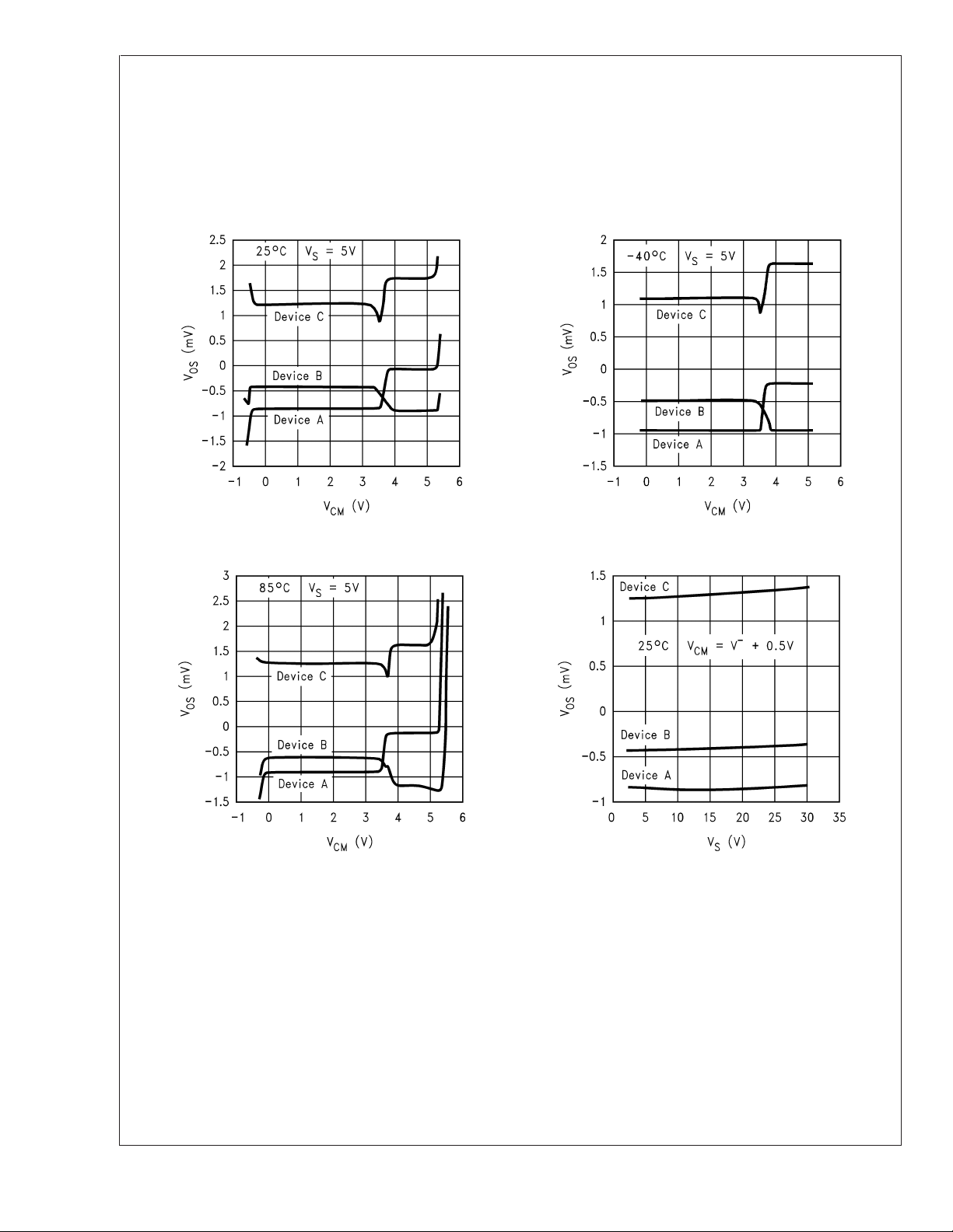
vs. VCMfor 3 Representative Units VOSvs. VCMfor 3 Representative Units
V
OS
>
TA.
J
10108430
VOSvs. VCMfor 3 Representative Units VOSvs. VSfor 3 Representative Units
10108431 10108434
10108429
www.national.com 6
LM8261
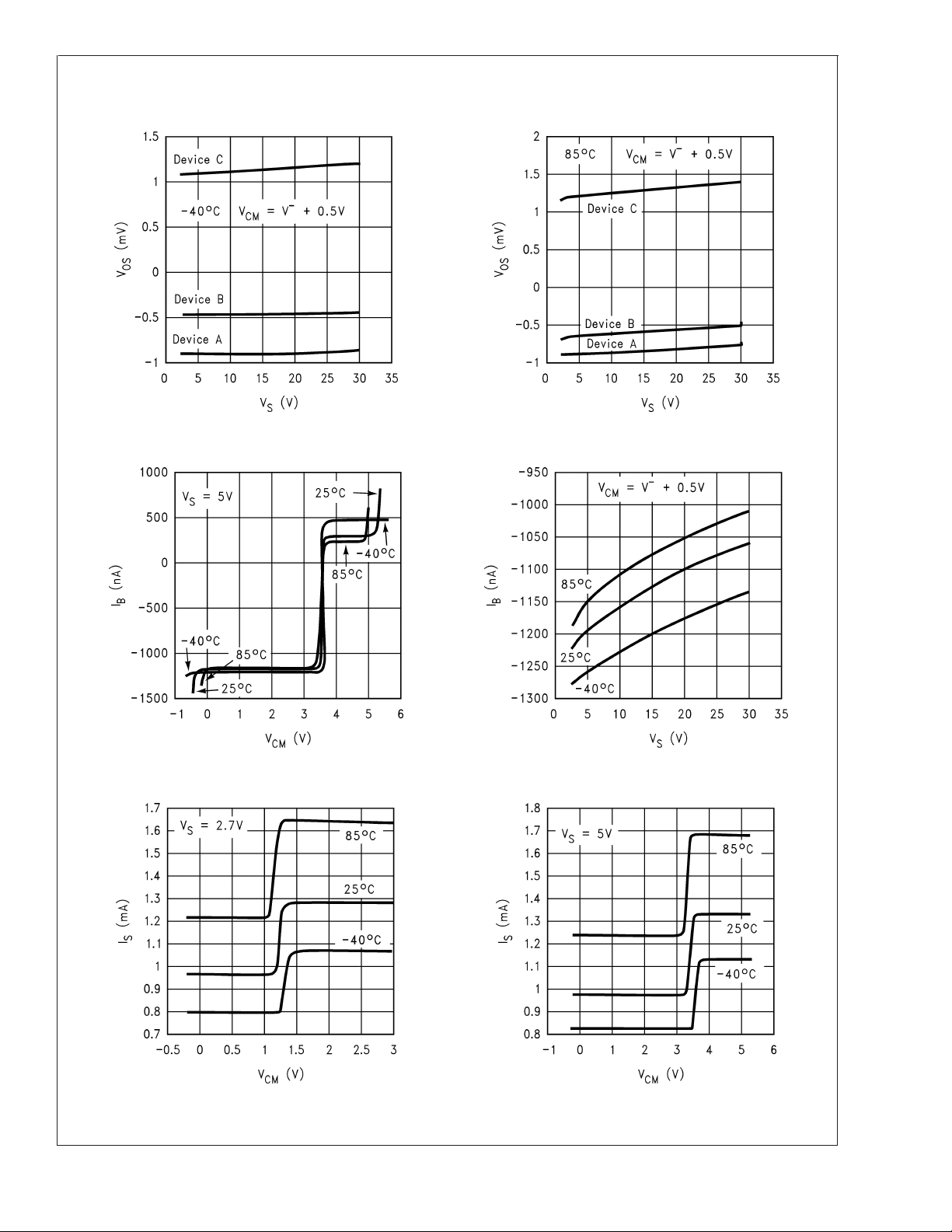
Typical Performance Characteristics T
V
vs. VSfor 3 Representative Units VOSvs. VSfor 3 Representative Units
OS
10108435
IBvs. V
CM
= 25˚C, Unless Otherwise Noted (Continued)
A
IBvs. V
S
10108433
ISvs. V
CM
10108424 10108436
ISvs. V
CM
10108427 10108428
www.national.com7