

National LM60BIM3, LM60CIM3 Schematic [ru]
LM60B/LM60C
2.7V, SOT-23 Temperature Sensor
Y
General Description
The LM60 is a precision integrated-circuit temperature sensor that can sense a
while operating from a single
output voltage is linearly proportional to Celsius (Centigrade) temperature (
a
424 mV. The offset allows reading negative temperatures
without the need for a negative supply. The nominal output
voltage of the LM60 ranges from
b
for a
40§Ctoa125§C temperature range. The LM60 is
calibrated to provide accuracies of
ature and
g
ture range.
The LM60’s linear output,
bration simplify external circuitry required in a single supply
environment where reading negative temperatures is required. Because the LM60’s quiescent current is less than
110 mA, self-heating is limited to a very low 0.1
Shutdown capability for the LM60 is intrinsic because its
inherent low power consumption allows it to be powered
directly from the output of many logic gates.
b
40§Ctoa125§C temperature range
a
2.7V supply. The LM60’s
a
6.25 mV/§C) and has a DC offset of
a
174 mV toa1205 mV
g
2.0§C at room temper-
3§C over the fullb25§Ctoa125§C tempera-
a
424 mV offset, and factory cali-
C in still air.
§
Applications
Y
Cellular Phones
Y
Computers
Power Supply Modules
Y
Battery Management
Y
FAX Machines
Y
Printers
Y
HVAC
Y
Disk Drives
Y
Appliances
Features
Y
Calibrated linear scale factor ofa6.25 mV/§C
Y
Rated for fullb40§toa125§C range
Y
Suitable for remote applications
Key Specifications
Y
Accuracy at 25§C
Y
Accuracy forb40§Ctoa125§C
Y
Accuracy forb25§Ctoa125§C
Y
Temperature Slope
Y
Power Supply Voltage Range
Y
Current Drain@25§C 110 mA (max)
Y
Nonlinearity
Y
Output Impedance 800X (max)
April 1996
g
2.0 andg3.0§C (max)
g
4.0§C (max)
g
3.0§C (max)
a
6.25 mV/§C
a
2.7V toa10V
g
0.8§C (max)
LM60B/LM60C 2.7V, SOT-23 Temperature Sensor
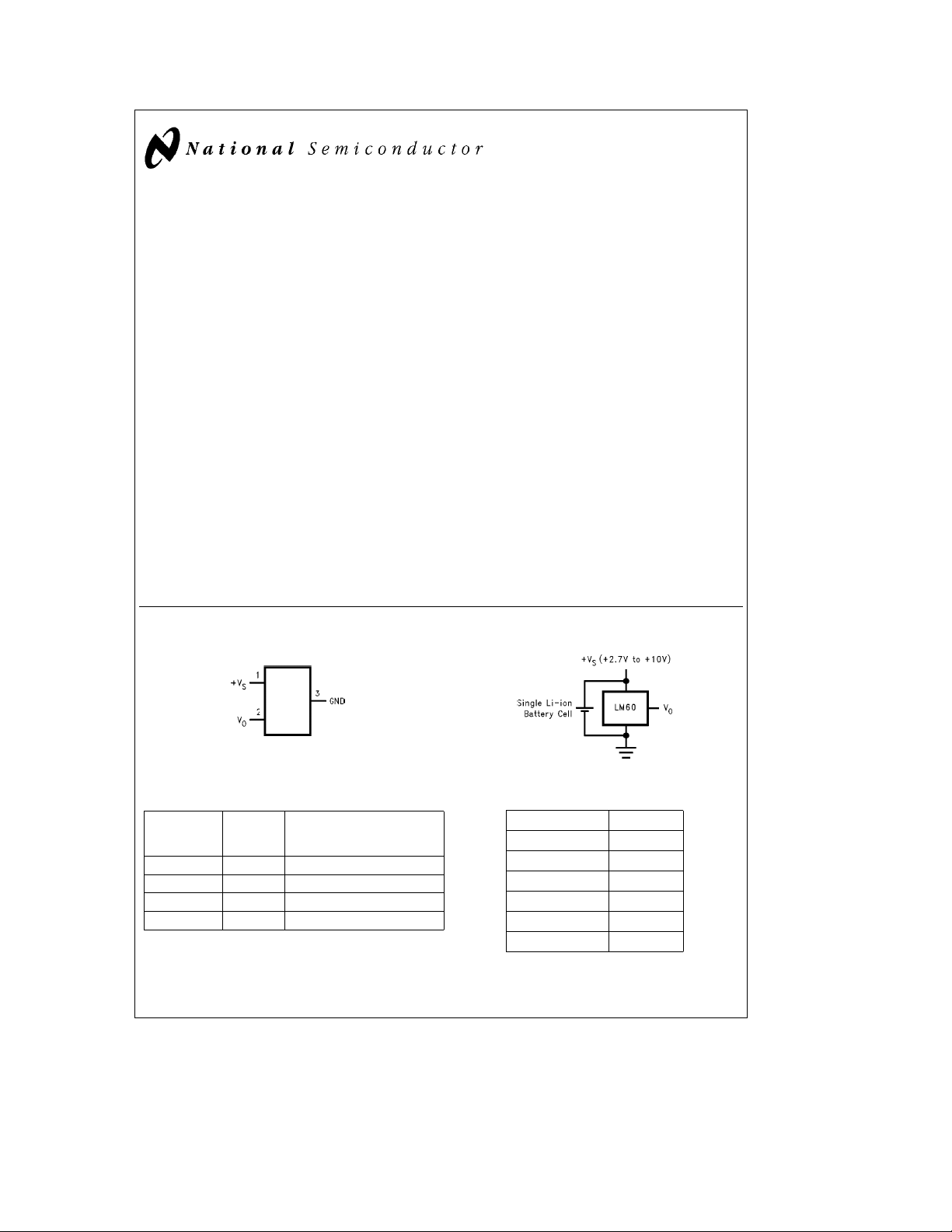
Connection Diagram
Typical Application
SOT-23
Top View
TL/H/12681– 1
See NS Package Number MA03B
Order Information
Order
Number
SOT-23
Device Supplied As
Marking
LM60BIM3 T6B 250 Units on Tape and Reel
LM60BIM3X T6B 3000 Units on Tape and Reel
LM60CIM3 T6C 250 Units on Tape and Reel
LM60CIM3X T6C 3000 Units on Tape and Reel
FIGURE 1. Full-Range Centigrade Temperature Sensor
(
e(a
V
6.25 mV/§CcT§C)a424 mV
O
Temperature (T) Typical V
a
125§C
a
100§C
a
25§C
0§C
b
25§C
b
40§C
b
40§Ctoa125§C) Operating from a Single Li-Ion
Battery Cell
C
1996 National Semiconductor Corporation RRD-B30M56/Printed in U. S. A.
TL/H/12681
a
1205 mV
a
1049 mV
a
580 mV
a
424 mV
a
268 mV
a
174 mV
TL/H/12681– 2
O

Absolute Maximum Ratings (Note 1)
a
Supply Voltage
Output Voltage (
a
Output Current 10 mA
a
V
0.6V) tob0.6V
S
12V tob0.2V
Input Current at any pin (Note 2) 5 mA
JMAX
)
b
65§Ctoa150§C
a
125§C
Storage Temperature
Maximum Junction Temperature (T
ESD Susceptibility (Note 3):
Human Body Model 800V
Machine Model 200V
Electrical Characteristics Unless otherwise noted, these specifications apply for
e
I
1 mA. Boldface limits apply for T
LOAD
e
e
T
A
J
Parameter Conditions
Accuracy (Note 8)
Output Voltage at 0§C
Nonlinearity (Note 9)
Sensor Gain
(Average Slope)
Output Impedance 800 800 X (max)
Line Regulation (Note 10)
Quiescent Current
Change of Quiescent
Current
a
a
a
a
3.0V
2.7V
2.7V
2.7V
a
a
V
10V
S
s
s
a
a
V
3.3V
S
s
s
a
a
V
10V
S
s
s
a
a
V
10V
S
s
s
Temperature Coefficient of
Quiescent Current
e
Long Term Stability (Note 11) T
Note 1: Absolute Maximum Ratings indicate limits beyond which damage to the device may occur. Operating Ratings indicate conditions for which the device is
functional, but do not guarantee specific performance limits. For guaranteed specifications and test conditions, see the Electrical Characteristics. The guaranteed
specifications apply only for the test conditions listed. Some performance characteristics may degrade when the device is not operated under the listed test
conditions.
Note 2: When the input voltage (V
Note 3: The human body model is a 100 pF capacitor discharged through a 1.5 kX resistor into each pin. The machine model is a 200 pF capacitor discharged
directly into each pin.
Note 4: See AN-450 ‘‘Surface Mounting Methods and Their Effect on Product Reliability’’ or the section titled ‘‘Surface Mount’’ found in any post 1986 National
Semiconductor Linear Data Book for other methods of soldering surface mount devices.
Note 5: The junction to ambient thermal resistance ( i
Note 6: Typicals are at T
Note 7: Limits are guaranteed to National’s AOQL (Average Outgoing Quality Level).
Note 8: Accuracy is defined as the error between the output voltage and
voltage, current, and temperature (expressed in
Note 9: Nonlinearity is defined as the deviation of the output-voltage-versus-temperature curve from the best-fit straight line, over the device’s rated temperature
range.
Note 10: Regulation is measured at constant junction temperature, using pulse testing with a low duty cycle. Changes in output due to heating effects can be
computed by multiplying the internal dissipation by the thermal resistance.
Note 11: For best long-term stability, any precision circuit will give best results if the unit is aged at a warm temperature, and/or temperature cycled for at least 46
hours before long-term life test begins. This is especially true when a small (Surface-Mount) part is wave-soldered; allow time for stress relaxation to occur. The
majority of the drift will occur in the first 1000 hours at elevated temperatures. The drift after 1000 hours will not continue at the first 1000 hour rate.
) at any pin exceeds power supplies (V
I
e
e
T
25§C and represent most likely parametric norm.
J
A
ea
T
J
1000 hours
C).
§
125§C, for
MAX
) is specified without a heat sink in still air.
JA
a
Lead Temperature
SOT Package (Note 4):
Vapor Phase (60 seconds)
Infrared (15 seconds)
a
a
215§C
220§C
Operating Ratings (Note 1)
s
Specified Temperature Range: T
LM60C
LM60B
b
40§CsT
b
25§CsT
MIN
Supply Voltage Range (aVS)
Thermal Resistance, iJA(Note 5) 450§C/W
a
ea
V
T
to T
MIN
; all other limits T
MAX
Typical
(Note 6)
a
424 mV
a
6.25
82
LM60B LM60C
Limits Limits
(Note 7) (Note 7)
g
g
g
a
a
g
g
125 125 mA (max)
g
g
e
A
2.0
3.0
0.6
6.06
6.44
0.3
2.3
110 110 mA (max)
5.0
20
S
e
T
25§C.
J
g
3.0
g
4.0
g
0.8
a
6.00 mV/§C (min)
a
6.50 mV/§C (max)
g
0.3 mV/V (max)
g
2.3 mV (max)
g
5.0 mA (max)
g
20 mA (max)
0.2 mA/
g
0.2
k
I
6.25 mV/§C times the device’s case temperature plus 424 mV, at specified conditions of
GND or V
l
a
VS), the current at that pin should be limited to 5 mA.
I
s
T
A
s
a
A
s
a
A
a
2.7V toa10V
3.0 VDCand
Units
(Limit)
C (max)
§
C (max)
§
C (max)
§
C
§
T
MAX
125§C
125§C
C
§
http://www.national.com 2
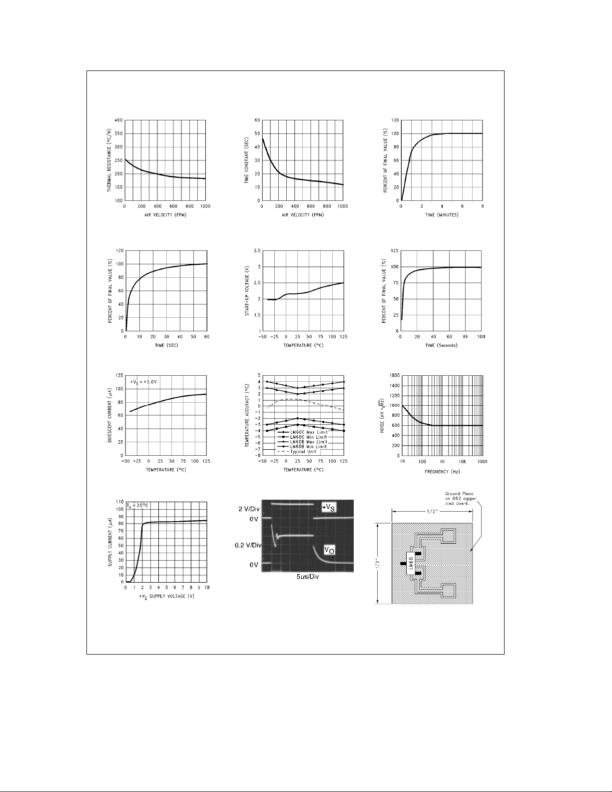
Typical Performance Characteristics
To generate these curves the LM60 was mounted to a printed circuit board as shown in
Thermal Resistance
Junction to Air
Thermal Time Constant
Figure 2
.
Thermal Response in
Still Air with Heat Sink
Thermal Response
in Stirred Oil Bath
with Heat Sink
Quiescent Current
vs. Temperature
Supply Voltage
vs Supply Current
TL/H/12681– 3
TL/H/12681– 6
TL/H/12681– 9
TL/H/12681– 4
Start-Up Voltage
vs. Temperature
TL/H/12681– 7
Accuracy vs Temperature
TL/H/12681– 10
Start-Up Response
TL/H/12681– 5
Thermal Response in Still
Air without a Heat Sink
TL/H/12681– 8
Noise Voltage
TL/H/12681– 11
TL/H/12681– 12
TL/H/12681– 13
FIGURE 2. Printed Circuit Board Used
TL/H/12681– 14
for Heat Sink to Generate All Curves.
(/2
Square Printed Circuit Board
×
with 2 oz. Copper Foil or Similar.
http://www.national.com3
 Loading...