

National LM4132AMF-2.0, LM4132AMF-2.5, LM4132AMF-4.1, LM4132BMF-2.0, LM4132BMF-2.5 Schematic [ru]
...
LM4132
SOT-23 Precision Low Dropout Voltage Reference
LM4132 SOT-23 Precision Low Dropout Voltage Reference
September 2005
General Description
The LM4132 family of precision voltage references performs
comparable to the best laser-trimmed bipolar references, but
in cost effective CMOS technology. The key to this break
through is the use of EEPROM registers for correction of
curvature, tempco, and accuracy on a CMOS bandgap architecture that allows package level programming to overcome assembly shift. The shifts in voltage accuracy and
tempco during assembly of die into plastic packages limit the
accuracy of references trimmed with laser techniques.
Unlike other LDO references, the LM4132 is capable of
delivering up to 20mA and does not require an output capacitor or buffer amplifier. These advantages and the SOT23
packaging are important for space-critical applications.
Series references provide lower power consumption than
shunt references, since they do not have to idle the maximum possible load current under no load conditions. This
advantage, the low quiescent current (60µA), and the low
dropout voltage (400mV) make the LM4132 ideal for batterypowered solutions.
The LM4132 is available in five grades (A, B, C, D and E) for
greater flexibility. The best grade devices (A) have an initial
accuracy of 0.05% with guaranteed temperature coefficient
of 10ppm/˚C or less, while the lowest grade parts (E) have
an initial accuracy of 0.5% and a tempco of 30ppm/˚C.
Features
n Output initial voltage accuracy 0.05%
n Low temperature coefficient 10ppm/˚C
n Low Supply Current, 60µA
n Enable pin allowing a 3µA shutdown mode
n 20mA output current
n Voltage options 2.048V, 2.5V, 4.096V
n Custom voltage options available (1.8V to 4.096V)
n V
range of V
IN
n Stable with low ESR ceramic capacitors
n SOT23-5 Package
+ 400mV to 5.5V@10mA
REF
Applications
n Instrumentation & Process Control
n Test Equipment
n Data Acquisition Systems
n Base Stations
n Servo Systems
n Portable, Battery Powered Equipment
n Automotive & Industrial
n Precision Regulators
n Battery Chargers
n Communications
n Medical Equipment
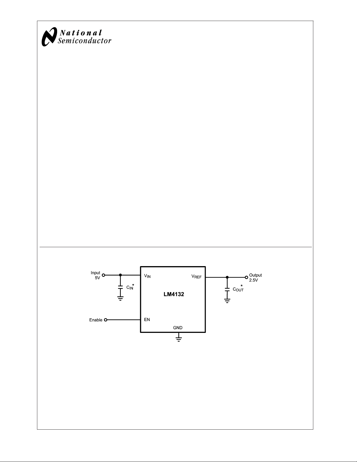
Typical Application Circuit
*Note: The capacitor CINis required and the capacitor C
OUT
is optional.
20151301
© 2005 National Semiconductor Corporation DS201513 www.national.com
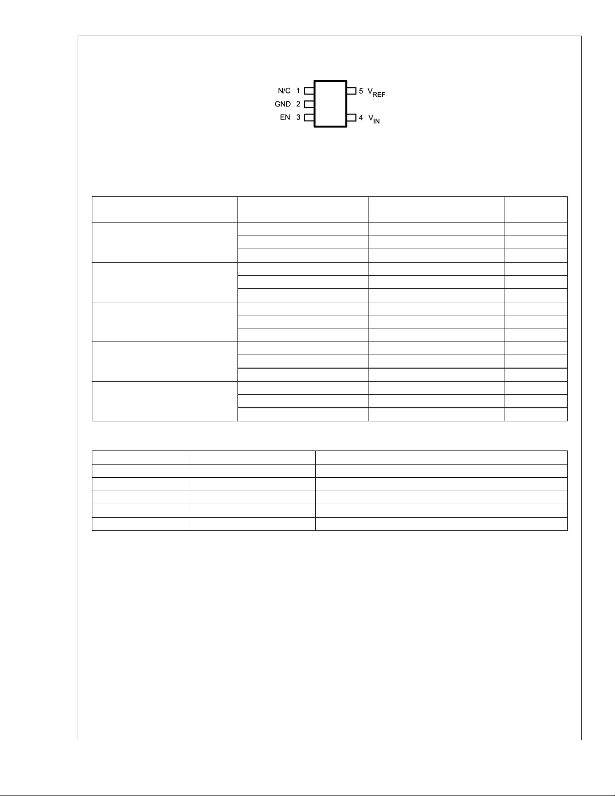
Connection Diagram
LM4132
Top View
SOT23-5 Package
NS Package Number MA05B
20151302
Ordering Information
Input Output Voltage Accuracy at
25˚C And Temperature Coefficient
0.05%, 10 ppm/˚C max (A grade) LM4132AMF-2.0 LM4132AMFX-2.0 R4BA
0.1%, 20 ppm/˚C max (B grade) LM4132BMF-2.0 LM4132BMFX-2.0 R4BB
0.2%, 20 ppm/˚C max (C grade) LM4132CMF-2.0 LM4132CMFX-2.0 R4BC
0.4%, 20 ppm/˚C max (D grade) LM4132DMF-2.0 LM4132DMFX-2.0 R4BD
0.5%, 30 ppm/˚C max (E grade) LM4132EMF-2.0 LM4132EMFX-2.0 R4BE
LM4132 Supplied as 1000
units, Tape and Reel
LM4132AMF-2.5 LM4132AMFX-2.5 R4CA
LM4132AMF-4.1 LM4132AMFX-4.1 R4FA
LM4132BMF-2.5 LM4132BMFX-2.5 R4CB
LM4132BMF-4.1 LM4132BMFX-4.1 R4FB
LM4132CMF-2.5 LM4132CMFX-2.5 R4CC
LM4132CMF-4.1 LM4132CMFX-4.1 R4FC
LM4132DMF-2.5 LM4132DMFX-2.5 R4CD
LM4132DMF-4.1 LM4132DMFX-4.1 R4FD
LM4132EMF-2.5 LM4132EMFX-2.5 R4CE
LM4132EMF-4.1 LM4132EMFX-4.1 R4FE
LM4132 Supplied as 3000 units,
Tape and Reel Part Marking
Pin Descriptions
Pin # Name Function
1 N/C No connect pin, leave floating
2 GND Ground
3 EN Enable pin
4V
5V
REF
IN
Input supply
Reference output
www.national.com 2
LM4132
Absolute Maximum Ratings (Note 1)
If Military/Aerospace specified devices are required,
please contact the National Semiconductor Sales Office/
Distributors for availability and specifications.
Maximum Voltage on any input -0.3 to 6V
Lead Temperature (soldering, 10sec) 260˚C
Vapor Phase (60 sec) 215˚C
Infrared (15sec) 220˚C
ESD Susceptibility (Note 3)
Human Body Model 2kV
Output short circuit duration Indefinite
Power Dissipation (T
= 25˚C)
A
Operating Ratings
(Note 2) 350mW
Storage Temperature Range −65˚C to 150˚C
Maximum Input Supply Voltage 5.5V
Maximum Enable Input Voltage V
Maximum Load Current 20mA
Junction Temperature Range (T
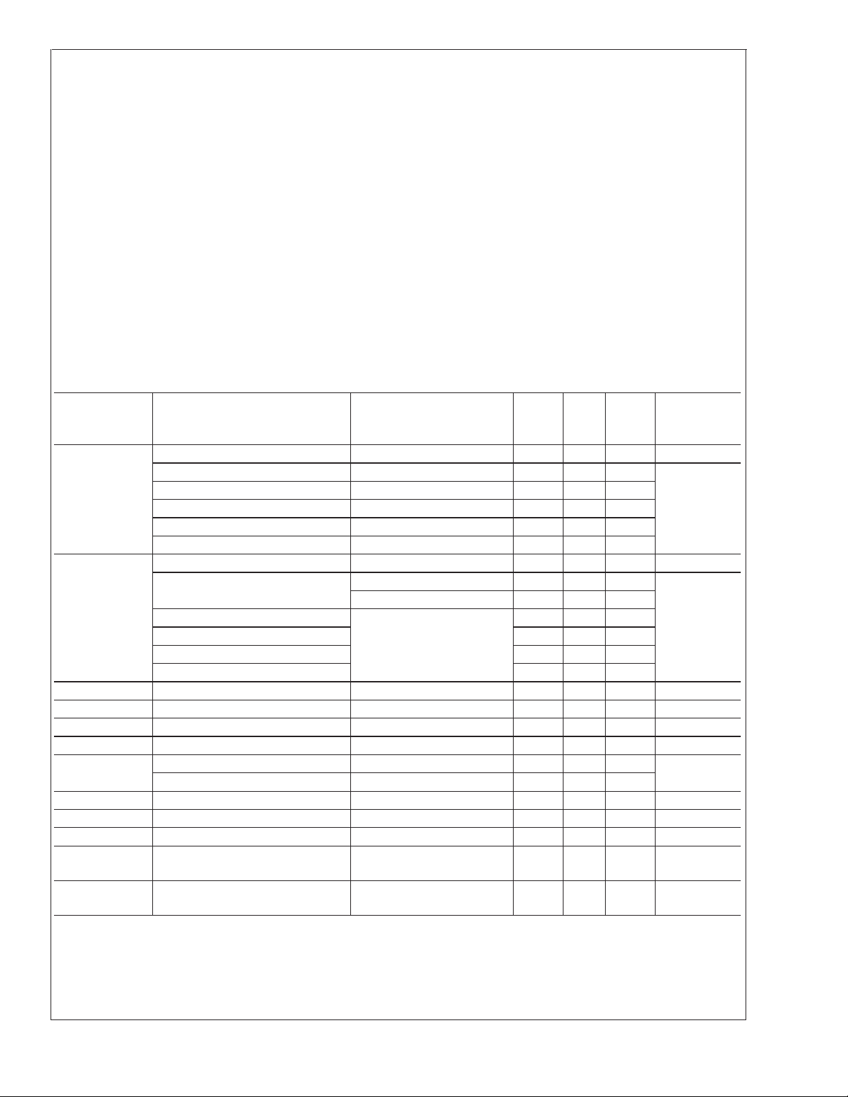
Electrical Characteristics
LM4132-2.0 (V
ply over the junction temperature (T
= 2.048V) Limits in standard type are for T
OUT
) range of -40˚C to +125˚C. Minimum and Maximum limits are guaranteed through test,
J
design, or statistical correlation. Typical values represent the most likely parametric norm at T
reference purposes only. Unless otherwise specified V
= 5V and I
IN
LOAD
=0
Symbol Parameter Conditions
V
REF
Output Voltage Initial Accuracy
LM4132A-2.0 (A Grade - 0.05%) -0.05 0.05 %
LM4132B-2.0 (B Grade - 0.1%) -0.1 0.1
LM4132C-2.0 (C Grade - 0.2%) -0.2 0.2
LM4132D-2.0 (D Grade - 0.4%) -0.4 0.4
LM4132E-2.0 (E Grade - 0.5%) -0.5 0.5
TCV
REF
(Note 6)
/˚C
Temperature Coefficient
LM4132A-2.0 0˚C ≤ T
-40˚C ≤ T
≤ + 85˚C 10
J
≤ +125˚C 20
J
LM4132B-2.0
LM4132C-2.0 20
LM4132D-2.0 20
-40˚C ≤ T
≤ +125˚C
J
LM4132E-2.0 30
∆V
∆V
REF
V
I
Q
I
Q_SD
/∆V
REF
/∆I
LOAD
∆V
REF
IN-VREF
V
N
I
SC
V
IL
Supply Current 60 100 µA
Supply Current in Shutdown EN = 0V 3 7 µA
Line Regulation V
IN
Load Regulation 0mA ≤ I
+ 400mV ≤ VIN≤ 5.5V 30 ppm / V
REF
≤ 20mA 25 120 ppm/mA
LOAD
Long Term Stability (Note 7) 1000 Hrs 50 ppm
Thermal Hysteresis (Note 8) -40˚C ≤ T
Dropout Voltage (Note 9) I
LOAD
≤ +125˚C 75
J
= 10mA 175 400 mV
Output Noise Voltage 0.1 Hz to 10 Hz 190 µV
Short Circuit Current 75 mA
Enable Pin Maximum Low Input
Level
V
IH
Enable Pin Minimum High Input
Level
= 25˚C only, and limits in boldface type ap-
J
Min
(Note 4)
65 %V
) −40˚C to
J
= 25˚C, and are provided for
J
Typ
(Note5)Max
(Note 4) Unit
20
ppm/˚C
35 %V
IN
+125˚C
PP
IN
IN
www.national.com3
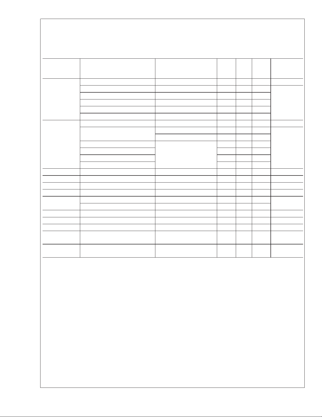
Electrical Characteristics
LM4132-2.5 (V
LM4132
over the junction temperature (T
sign, or statistical correlation. Typical values represent the most likely parametric norm at T
erence purposes only. Unless otherwise specified V
Symbol Parameter Conditions
V
REF
Output Voltage Initial Accuracy
LM4132A-2.5 (A Grade - 0.05%) -0.05 0.05 %
LM4132B-2.5 (B Grade - 0.1%) -0.1 0.1
LM4132C-2.5 (C Grade - 0.2%) -0.2 0.2
LM4132D-2.5 (D Grade - 0.4%) -0.4 0.4
LM4132E-2.5 (E Grade - 0.5%) -0.5 0.5
TCV
REF
(Note 6)
/˚C
Temperature Coefficient
LM4132A-2.5 0˚C ≤ T
LM4132B-2.5
LM4132C-2.5 20
LM4132D-2.5 20
LM4132E-2.5 30
∆V
∆V
REF
∆V
I
Q_SD
REF
I
Q
/∆I
REF
/∆V
LOAD
Supply Current 60 100 µA
Supply Current in Shutdown EN = 0V 3 7 µA
Line Regulation V
IN
Load Regulation 0mA ≤ I
Long Term Stability (Note 7) 1000 Hrs 50 ppm
Thermal Hysteresis (Note 8) -40˚C ≤ T
V
IN-VREF
V
I
SC
V
N
IL
Dropout Voltage (Note 9) I
Output Noise Voltage 0.1 Hz to 10 Hz 240 µV
Short Circuit Current 75 mA
Enable Pin Maximum Low Input
Level
V
IH
Enable Pin Minimum High Input
Level
= 2.5V) Limits in standard type are for T
OUT
) range of -40˚C to +125˚C. Minimum and Maximum limits are guaranteed through test, de-
J
= 5V and I
IN
-40˚C ≤ T
-40˚C ≤ T
REF
LOAD
J
=0
LOAD
≤ + 85˚C 10
J
≤ +125˚C 20
J
≤ +125˚C
J
+ 400mV ≤ VIN≤ 5.5V 50 ppm / V
≤ 20mA 25 120 ppm/mA
LOAD
≤ +125˚C 75
J
= 10mA 175 400 mV
= 25˚C only, and limits in boldface type apply
= 25˚C, and are provided for ref-
J
Typ
Min
(Note 4)
(Note5)Max
(Note 4) Unit
20
ppm/˚C
PP
35 %V
65 %V
IN
IN
www.national.com 4
Electrical Characteristics
LM4132-4.1 (V
ply over the junction temperature (T
= 4.096V) Limits in standard type are for T
OUT
) range of -40˚C to +125˚C. Minimum and Maximum limits are guaranteed through test,
J
design, or statistical correlation. Typical values represent the most likely parametric norm at T
reference purposes only. Unless otherwise specified V
= 5V and I
IN
LOAD
=0
Symbol Parameter Conditions
V
REF
Output Voltage Initial Accuracy
LM4132A-4.1 (A Grade - 0.05%) -0.05 0.05 %
LM4132B-4.1 (B Grade - 0.1%) -0.1 0.1
LM4132C-4.1 (C Grade - 0.2%) -0.2 0.2
LM4132D-4.1 (D Grade - 0.4%) -0.4 0.4
LM4132E-4.1 (E Grade - 0.5%) -0.5 0.5
TCV
REF
(Note 6)
/˚C
Temperature Coefficient
LM4132A-4.1 0˚C ≤ T
-40˚C ≤ T
≤ + 85˚C 10
J
≤ +125˚C 20
J
LM4132B-4.1
LM4132C-4.1 20
LM4132D-4.1 20
-40˚C ≤ T
≤ +125˚C
J
LM4132E-4.1 30
∆V
∆V
REF
V
I
Q
I
Q_SD
/∆V
REF
/∆I
LOAD
∆V
REF
IN-VREF
V
N
I
SC
V
IL
Supply Current 60 100 µA
Supply Current in Shutdown EN = 0V 3 7 µA
Line Regulation V
IN
Load Regulation 0mA ≤ I
+ 400mV ≤ VIN≤ 5.5V 100 ppm / V
REF
≤ 20mA 25 120 ppm/mA
LOAD
Long Term Stability (Note 7) 1000 Hrs 50 ppm
Thermal Hysteresis (Note 8) -40˚C ≤ T
Dropout Voltage (Note 9) I
LOAD
≤ +125˚C 75
J
= 10mA 175 400 mV
Output Noise Voltage 0.1 Hz to 10 Hz 350 µV
Short Circuit Current 75 mA
Enable Pin Maximum Low Input
Level
V
IH
Enable Pin Minimum High Input
Level
= 25˚C only, and limits in boldface type ap-
J
Min
(Note 4)
65 %V
= 25˚C, and are provided for
J
Typ
(Note5)Max
(Note 4) Unit
20
ppm/˚C
35 %V
LM4132
PP
IN
IN
Note 1: Absolute Maximum Ratings indicate limits beyond which damage may occur to the device. Operating Ratings indicate conditions for which the device is
intended to be functional, but do not guarantee specific performance limits. For guaranteed specifications, see Electrical Characteristics.
Note 2: Without PCB copper enhancements. The maximum power dissipation must be de-rated at elevated temperatures and is limited by T
junction temperature), θ
=(T
Note 3: The human body model is a 100 pF capacitor discharged through a 1.5 kΩ resistor into each pin.
Note 4: Limits are 100% production tested at 25˚C. Limits over the operating temperature range are guaranteed through correlation using Statistical Quality Control.
Note 5: Typical numbers are at 25˚C and represent the most likely parametric norm.
Note 6: Temperature coefficient is measured by the "Box" method; i.e., the maximum ∆V
Note 7: Long term stability is V
Note 8: Thermal hysteresis is defined as the change in +25˚C output voltage before and after cycling the device from (-40˚C to 125˚C).
Note 9: Dropout voltage is defined as the minimum input to output differential at which the output voltage drops by 0.5% below the value measured with a 5V input.
JMAX-TA
)/θ
(junction to ambient thermal resistance) and TA(ambient temperature). The maximum power dissipation at any temperature is: P
J-A
up to the value listed in the Absolute Maximum Ratings. θ
J-A
@
25˚C measured during 1000 hrs.
REF
for SOT23-5 package is 220˚C/W, T
J-A
is divided by the maximum ∆T.
REF
JMAX
= 125˚C.
JMAX
www.national.com5
(maximum
DissMAX
 Loading...