

National LM3620M5-4, LM3620M5-8 Schematic [ru]
LM3620
Lithium-Ion Battery Charger Controller
General Description
The LM3620 series of controllers are monolithic integrated
circuits designed to control the charging and end-of-charge
control for lithium-ion rechargeable batteries. The LM3620 is
available in two versions for one or two cell charger applications. Each version provides the option of selecting the
appropriate termination voltage for either coke or graphite
anode lithium cells.
The LM3620 can operate from a wide range of DC input
sources (4V to 30V). With no charger supply connected, the
controller draws a quiescent current of only 10nA to minimize
discharging of a connected battery pack.
The LM3620 consists of an operational transconductance
amplifier, a bandgap voltage reference, a NPN driver transistor and precision voltage setting resistors. The output of
the amplifier is made available to drive an external power
transistor if higher drive currents are required.
With a trimmed output voltage regulation of
accuracy, the LM3620 provides a simple, precise solution for
end-of-charge control of lithium-ion rechargeable cells.
The LM3620 is packaged in a miniature 5-lead SOT-23
surface mount package for very compact designs.
Features
n Voltage options for charging 1 or 2 cell stacks
n Adjustable output voltage for coke or graphite anodes
n Precision end-of-charge voltage control
n Wide input voltage range (4V to 30V)
n Low off state current (
n Drive provided for external power stage
n Tiny SOT-23 package
<
10nA)
July 2000
±
1.2% initial
LM3620 Lithium-Ion Battery Charger Controller
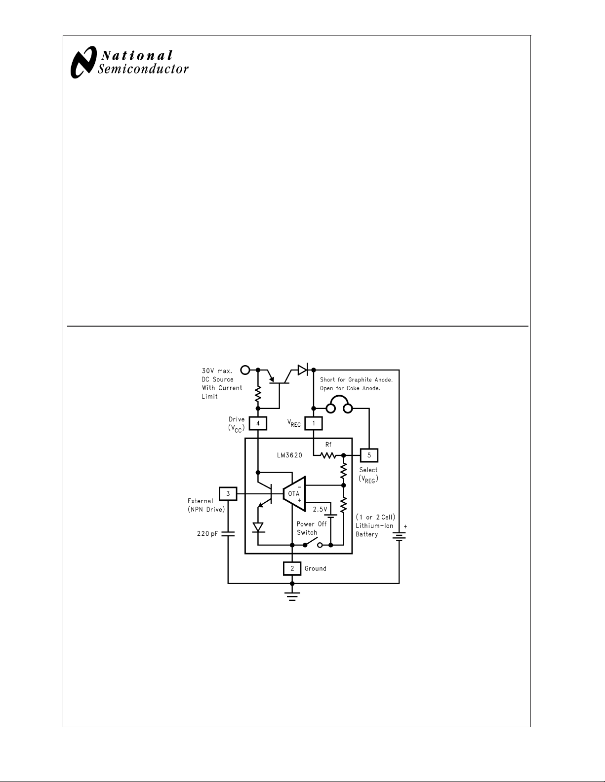
Typical Application
10084110
© 2004 National Semiconductor Corporation DS100841 www.national.com
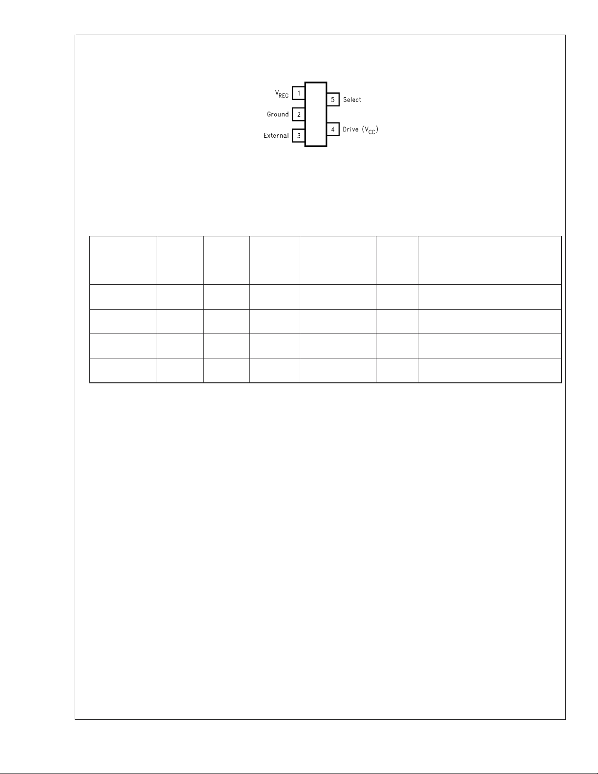
Connection Diagram
LM3620
5-Lead SOT23-5 Surface Mount Package
Refer to the Ordering Information Table in
this Data Sheet for Specific Part Number
See NS Package MF05A
10084101
Ordering Information
Device Order
Number
LM3620M5-4 D10B 4.1V/4.2V 1.2% 2% 1
LM3620M5X-4 D10B 4.1V/4.2V 1.2% 2% 1
LM3620M5-8 D11B 8.2V/8.4V 1.2% 2% 2
LM3620M5X-8 D11B 8.2V/8.4V 1.2% 2% 2
The small physical size of the SOT23-5 Package does not
allow for the full part number marking. Devices will be
marked with the designation shown in the column Package
Marking.
Package
Marking
Output
Voltage
Initial
Accuracy
(25˚C)
Over
Temperature
Accuracy
(0 to 70˚C)
The devices are shipped in tape-and-reel format. The standard quantity is 250 units on a reel (indicated by the letters
“M5” in the part number), or 3000 units on a reel (indicated
by the letters “M5X” in the part number).
Number
of Cells
Supplied as
1000 Unit increments on Tape and
Reel
3000 Unit increments on Tape and
Reel
1000 Unit increments on Tape and
Reel
3000 Unit increments on Tape and
Reel
www.national.com 2
LM3620
Absolute Maximum Ratings (Note 1)
If Military/Aerospace specified devices are required,
please contact the National Semiconductor Sales Office/
Power Dissipation (T
= 25˚C)
A
(Note 2)
ESD Susceptibility (Note 3) 2000V
Distributors for availability and specifications.
Input Voltage (V
V
EXT
Junction Temperature 150˚C
Storage Temperature −65 to +150˚C
Lead Temp. Soldering
Vapor Phase (60 sec.)
Infrared (15 sec.)
) 35V
DRIVE
1.5V
215˚C
220˚C
Operating Ratings (Note 1)
Ambient Temp. Range 0˚C to 70˚C
Junction Temp. Range 0˚C to 125˚C
Thermal Resistance (Junction to
Ambient, θ
Input Voltage (V
J-A
)
) 4Vto30V
DRIVE
280˚C/W
Electrical Characteristics
LM3620-4
V
= 5V, I
DRIVE
limits with standard typeface apply for T
Symbol Parameter Conditions Typical Limit Units
V
REG
V
REG/VDRIVE
I
Q
I
OFF
I
DRIVE
Gm
(DRIVE)
I
EXT
Gm
(EXT)
R
IN
R
F
= 2mA. Limits with boldface type apply over the full operating ambient temperature range, 0˚C to +70˚C,
DRIVE
Regulated Output Voltage (pin 1
to ground)
= 25˚C.
A
Pin 5 shorted to pin 1 (graphite
anode)
4.1 4.051/4.018 V(min)
4.149/4.182 V(max)
Pin 5 open (coke anode) 4.2 4.150/4.116 V(min)
4.250/4.284 V(max)
Regulated Output Voltage
Either Pin 5 setting
±
1.2/±2.0 %
Tolerance
Supply Sensitivity V
Quiescent Current V
Off State Current V
Drive Pin Sink Current V
Drive Pin Transconductance ∆I
External Pin Source Current V
External Pin Transconductance ∆I
V
Input Resistance Pin 1 to Ground.
REG
for 5V ≤ V
REG
= 4.5V, V
REG
open circuited (Note 5) 10 200 nA(max)
DRIVE
= 5.0V 20 15 mA(min)
DRIVE
/∆V
DRIVE
2mA ≤ I
EXT
EXT
0mA ≤ I
REG
≤15mA
DRIVE
= 1V (Note 6) 3 2.5 mA(min)
/∆V
REG,VEXT
≤ 2.5mA
EXT
Circuit biased with V
open circuited
V
DRIVE
≤ 30V 100 µV/V(max)
DRIVE
= 1.0V (Note 4) 400 750 µA(max)
EXT
3 A/V
=1V
DRIVE
applied
0.8 A/V
46 kΩ
42 MΩ
Feedback Resistance Pin 1 to Pin 5 1500 Ω
300mW
www.national.com3
 Loading...