

National LM3500TL-16, LM3500TL-21 Schematic [ru]
February 2005
LM3500
Synchronous Step-up DC/DC Converter for White LED
Applications
LM3500 Synchronous Step-up DC/DC Converter for White LED Applications
General Description
The LM3500 is a fixed-frequency step-up DC/DC converter
that is ideal for driving white LEDs for display backlighting and
other lighting functions. With fully intergrated synchronous
switching (no external schottky diode required) and a low
feedback voltage (500mV), power efficiency of the LM3500
circuit has been optimized for lighting applications in wireless
phones and other portable products (single cell Li-Ion or 3cell NiMH battery supplies). The LM3500 operates with a fixed
1MHz switching frequency. When used with ceramic input
and output capacitors, the LM3500 provides a small, lownoise, low-cost solution.
Two LM3500 options are available with different output voltage capabilities. The LM3500-21 has a maximum output
voltage of 21V and is typically suited for driving 4 or 5 white
LEDs in series. The LM3500-16 has a maximum output voltage of 16V and is typically suited for driving 3 or 4 white LEDs
in series (maximum number of series LEDs dependent on
LED forward voltage). If the primary white LED network
should be disconnected, the LM3500 uses internal protection
circuitry on the output to prevent a destructive over-voltage
event.
A single external resistor is used to set the maximum LED
current in LED-drive applications. The LED current can easily
be adjusted using a pulse width modulated (PWM) signal on
the shutdown pin. In shutdown, the LM3500 completely disconnects the input from output, creating total isolation and
preventing any leakage currents from trickling into the LEDs.
Features
Synchronous rectification, high efficiency and no external
■
schottky diode required
Uses small surface mount components
■
Can drive 2-5 white LEDs in series
■
(may function with more low-VF LEDs)
2.7V to 7V input range
■
Internal output over-voltage protection (OVP) circuitry,
■
with no external zener diode required
LM3500-16: 15.5V OVP; LM3500-21: 20.5V OVP.
True shutdown isolation
■
Input undervoltage lockout
■
Requires only small ceramic capacitors at the input and
■
output
Thermal Shutdown
■
0.1µA shutdown current
■
Small 8-bump thin micro SMD package
■
Applications
LCD Bias Supplies
■
White LED Backlighting
■
Handheld Devices
■
Digital Cameras
■
Portable Applications
■
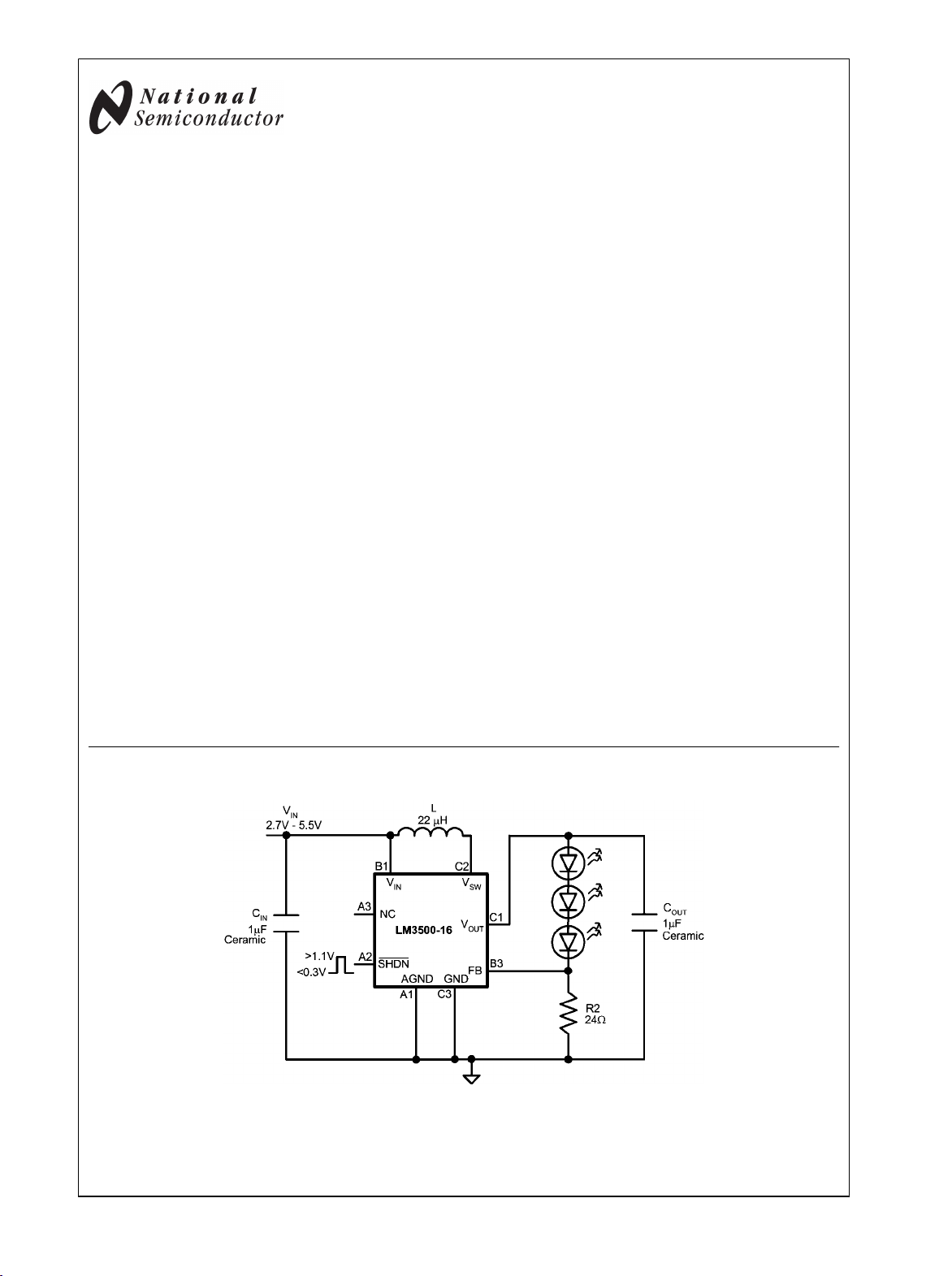
Typical Application Circuit
20065701
© 2007 National Semiconductor Corporation 200657 www.national.com
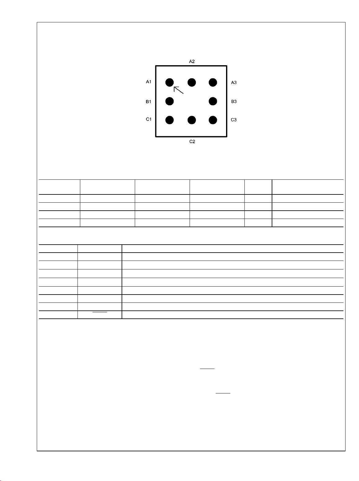
Connection Diagram
LM3500
Top View
8-bump micro SMD
20065702
Ordering Information
Maximum
Output Voltage
16V LM3500TL-16 micro SMD TL08SSA S18 250 Units, Tape and Reel
16V LM3500TLX-16 micro SMD TL08SSA S18 3000 Units, Tape and Reel
21V LM3500TL-21 micro SMD TL08SSA S23 250 Units, Tape and Reel
21V LM3500TLX-21 micro SMD TL08SSA S23 3000 Units, Tape and Reel
Order Number Package Type NSC Package
Drawing
Top Mark Supplied As
Pin Description/Functions
Pin Name Function
A1 AGND Analog ground.
B1 V
C1 V
C2 V
C3 GND Power Ground.
B3 FB Output voltage feedback connection.
A3 NC No internal connection made to this pin.
A2 SHDN Shutdown control pin.
AGND(pin A1): Analog ground pin. The analog ground pin
should tie directly to the GND pin.
VIN(pin B1): Analog and Power supply pin. Bypass this pin
with a capacitor, as close to the device as possible, connected
between the VIN and GND pins.
V
(pin C1): Source connection of internal PMOS power
OUT
device. Connect the output capacitor between the V
GND pins as close as possible to the device.
VSW(pin C2): Drain connection of internal NMOS and PMOS
switch devices. Keep the inductor connection close to this pin
to minimize EMI radiation.
GND(pin C3): Power ground pin. Tie directly to ground plane.
IN
OUT
SW
Analog and Power supply input.
PMOS source connection for synchronous rectification.
Switch pin. Drain connections of both NMOS and PMOS power devices.
FB(pin B3): Output voltage feedback connection. Set the primary White LED network current with a resistor from the FB
pin to GND. Keep the current setting resistor close to the device and connected between the FB and GND pins.
NC(pin A3): No internal connection is made to this pin. The
maximum allowable voltage that can be applied to this pin is
OUT
and
7.5V.
SHDN(pin A2): Shutdown control pin. Disable the device with
a voltage less than 0.3V and enable the device with a voltage
greater than 1.1V. The white LED current can be controlled
using a PWM signal at this pin. There is an internal pull down
on the SHDN pin, the device is in a normally off state.
www.national.com 2
LM3500
Absolute Maximum Ratings (Note 1)
If Military/Aerospace specified devices are required,
please contact the National Semiconductor Sales Office/
Distributors for availability and specifications.
V
IN
V
(LM3500-16)(Note 2)
OUT
V
(LM3500-21)(Note 2)
OUT
VSW(Note 2) −0.3V to V
FB, SHDN, and NC Voltages −0.3V to 7.5V
−0.3V to 7.5V
−0.3V to 16V
−0.3V to 21V
+0.3V
OUT
Operating Conditions
Ambient Temperature
(Note 5) −40°C to +85°C
Junction Temperature −40°C to +125°C
Supply Voltage 2.7V to 7V
Thermal Properties
Junction to Ambient Thermal
Resistance (θJA)(Note 6)
75°C/W
Maximum Junction Temperature 150°C
Lead Temperature
(Note 3) 300°C
ESD Ratings (Note 4)
Human Body Model 2kV
Machine Model 200V
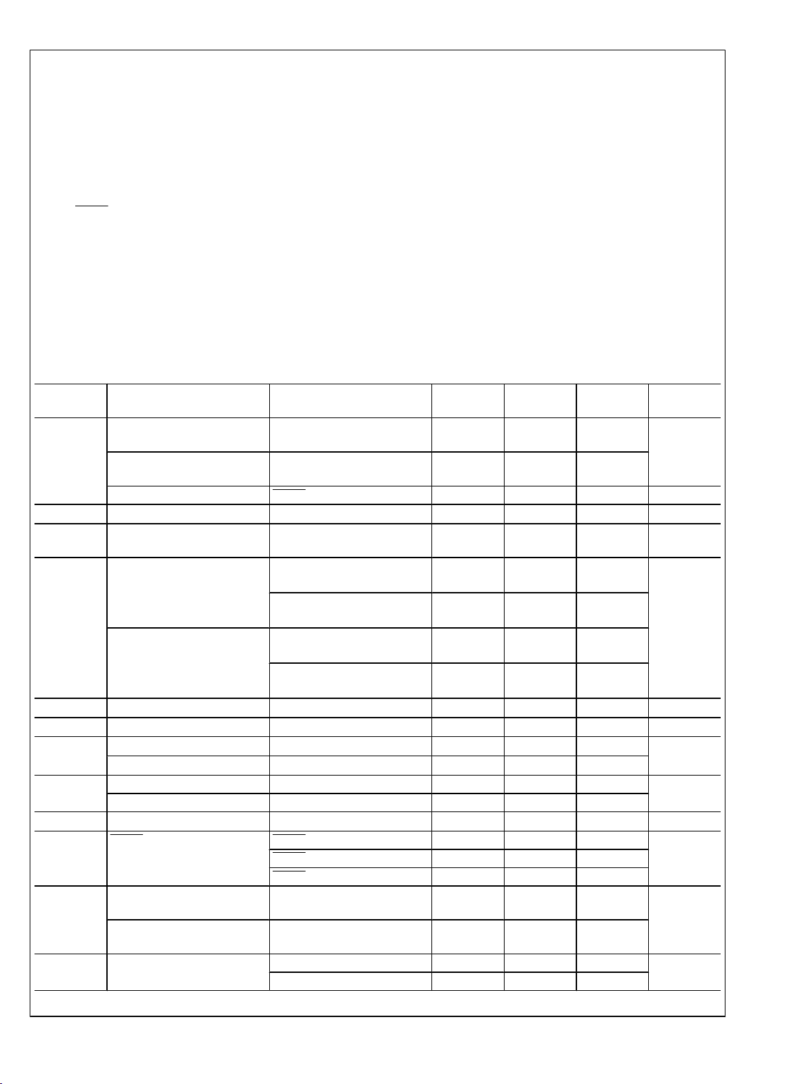
Electrical Characteristics
Specifications in standard type face are for TA = 25°C and those in boldface type apply over the Operating Temperature Range
of TA = −10°C to +85°C. Unless otherwise specified VIN =2.7V and specification apply to both LM3500-16 and LM3500-21.
Symbol Parameter Conditions
I
Q
Quiescent Current, Device Not
Switching
Quiescent Current, Device
Switching
FB > 0.54V
FB = 0V
Min
(Note 7)
Shutdown SHDN = 0V 0.1 2 µA
V
ΔV
FB
FB
Feedback Voltage VIN = 2.7V to 7V 0.47 0.5 0.53
Feedback Voltage Line
VIN = 2.7V to 7V
Regulation
I
CL
I
B
V
R
D
IN
DSON
Limit
Switch Current Limit
(LM3500-16)
Switch Current Limit
(LM3500-21)
VIN = 2.7V,
Duty Cycle = 80%
VIN = 3.0V,
Duty Cycle = 70%
VIN = 2.7V,
Duty Cycle = 70%
VIN = 3.0V,
Duty Cycle = 63%
275 400 480
255 400 530
420 640 770
450 670 800
FB Pin Bias Current FB = 0.5V (Note 9)
Input Voltage Range 2.7 7.0 V
NMOS Switch R
PMOS Switch R
DSON
DSON
VIN = 2.7V, ISW = 300mA
V
= 6V, ISW = 300mA
OUT
Duty Cycle Limit (LM3500-16) FB = 0V 80 87
Duty Cycle Limit (LM3500-21) FB = 0V 85 94
F
SW
I
SD
Switching Frequency
0.85 1.0 1.15 MHz
SHDN Pin Current (Note 10) SHDN = 5.5V 18 30
SHDN = GND 0.1
I
L
Switch Leakage Current
VSW = 15V 0.01 0.5 µA
(LM3500-16)
Switch Leakage Current
VSW = 20V 0.01 2.0
(LM3500-21)
UVP Input Undervoltage Lockout ON Threshold 2.4 2.5 2.6
OFF Threshold 2.3 2.4 2.5
Typ
(Note 8)
Max
(Note 7)
0.95 1.2
1.8 2.5
0.1 0.4 %/V
45 200 nA
0.43
1.1 2.3
Units
mA
V
mA
Ω
%
µASHDN = 2.7V 9 16
V
3 www.national.com
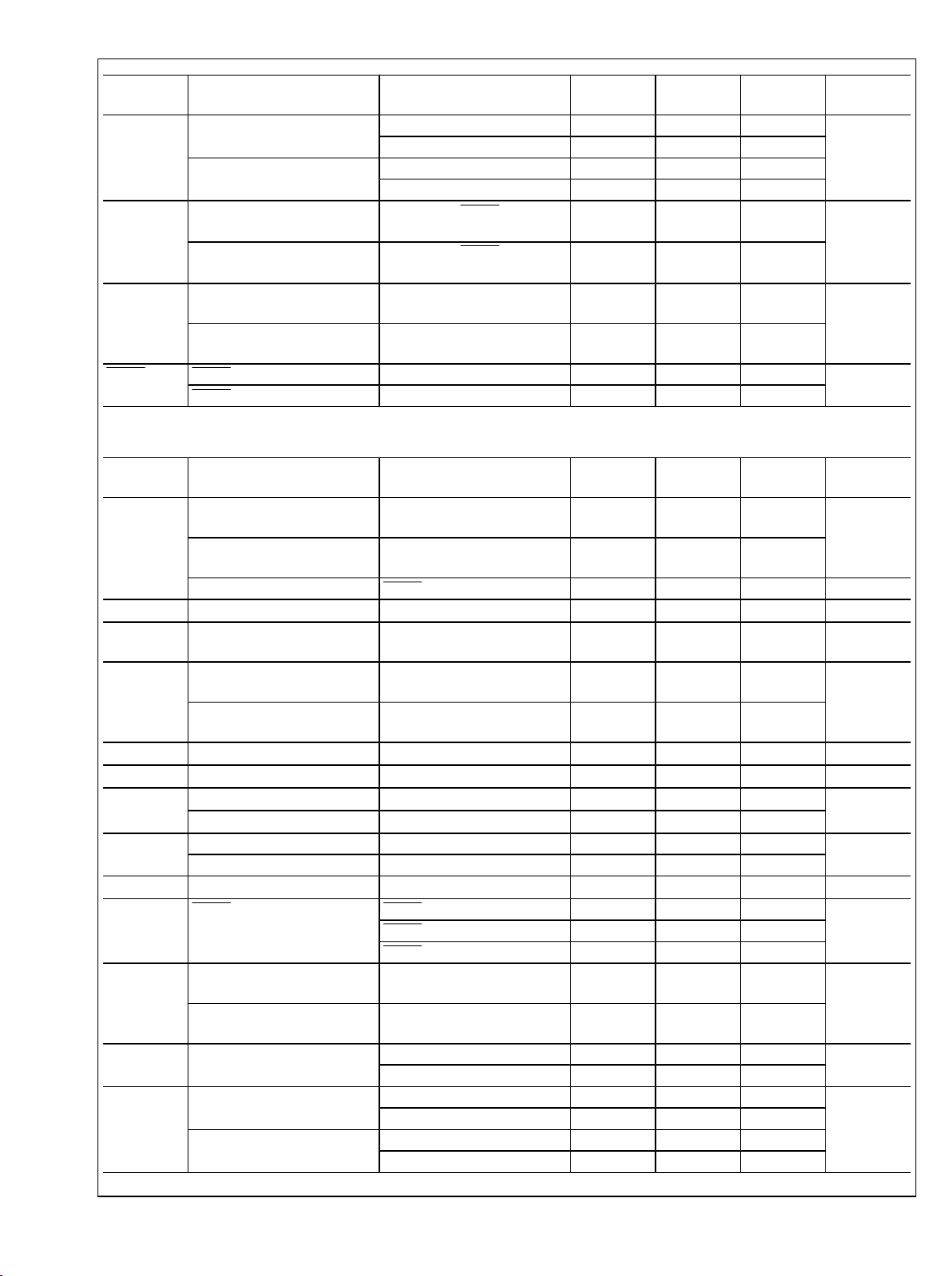
Symbol Parameter Conditions
LM3500
OVP Output Overvoltage Protection
(LM3500-16)
Output Overvoltage Protection
(LM3500-21)
I
Vout
V
Bias Current
OUT
ON Threshold 15 15.5 16
OFF Threshold 14 14.6 15
ON Threshold 20 20.5 21
OFF Threshold 19 19.5 20
V
= 15V, SHDN = V
OUT
(LM3500-16)
V
Bias Current
OUT
V
= 20V, SHDN = V
OUT
(LM3500-21)
I
VL
PMOS Switch Leakage
V
= 15V, VSW = 0V
OUT
Current (LM3500-16)
PMOS Switch Leakage
V
= 20V, VSW = 0V
OUT
Current (LM3500-21)
SHDN
Threshold
SHDN Low 0.65 0.3
SHDN High 1.1 0.65
Min
(Note 7)
IN
IN
Typ
(Note 8)
260 400
300 460
0.01 3
0.01 3
Max
(Note 7)
Specifications in standard type face are for TJ = 25°C and those in boldface type apply over the full Operating Temperature
Range (TJ = −40°C to +125°C). Unless otherwise specified VIN =2.7V and specification apply to both LM3500-16 and LM3500-21.
Symbol Parameter Conditions
I
Q
Quiescent Current, Device Not
Switching
Quiescent Current, Device
Switching
FB > 0.54V
FB = 0V
Min
(Note 7)
Typ
(Note 8)
0.95 1.2
1.8 2.5
Max
(Note 7)
Shutdown SHDN = 0V 0.1 2 µA
V
ΔV
I
CL
I
B
V
R
D
FB
FB
IN
DSON
Limit
Feedback Voltage VIN = 2.7V to 7V 0.47 0.5 0.53
Feedback Voltage Line
Regulation
Switch Current Limit
(LM3500-16)
Switch Current Limit
(LM3500-21)
FB Pin Bias Current FB = 0.5V (Note 9)
VIN = 2.7V to 7V
VIN = 3.0V, Duty Cycle = 70%
VIN = 3.0V, Duty Cycle = 63%
0.1 0.4 %/V
400
670
45 200 nA
Input Voltage Range 2.7 7.0 V
NMOS Switch R
PMOS Switch R
DSON
DSON
VIN = 2.7V, ISW = 300mA
V
= 6V, ISW = 300mA
OUT
0.43
1.1 2.3
Duty Cycle Limit (LM3500-16) FB = 0V 87
Duty Cycle Limit (LM3500-21) FB = 0V 94
F
SW
I
SD
Switching Frequency
0.8 1.0 1.2 MHz
SHDN Pin Current (Note 10) SHDN = 5.5V 18 30
SHDN = GND 0.1
I
L
Switch Leakage Current
VSW = 15V 0.01 0.5 µA
(LM3500-16)
Switch Leakage Current
VSW = 20V 0.01 2.0
(LM3500-21)
UVP Input Undervoltage Lockout ON Threshold 2.4 2.5 2.6
OFF Threshold 2.3 2.4 2.5
OVP Output Overvoltage Protection
(LM3500-16)
Output Overvoltage Protection
(LM3500-21)
ON Threshold 15 15.5 16
OFF Threshold 14 14.6 15
ON Threshold 20 20.5 21
OFF Threshold 19 19.5 20
Units
V
µA
µA
V
Units
mA
V
mA
Ω
%
µASHDN = 2.7V 9 16
V
V
www.national.com 4
LM3500
Symbol Parameter Conditions
I
Vout
V
Bias Current
OUT
V
= 15V, SHDN = V
OUT
IN
Min
(Note 7)
(LM3500-16)
V
Bias Current
OUT
V
= 20V, SHDN = V
OUT
IN
(LM3500-21)
I
VL
PMOS Switch Leakage
V
= 15V, VSW = 0V
OUT
Current (LM3500-16)
PMOS Switch Leakage
V
= 20V, VSW = 0V
OUT
Current (LM3500-21)
SHDN
Threshold
Note 1: Absolute maximum ratings are limits beyond which damage to the device may occur. Operating Ratings are conditions for which the device is intended
to be functional, but device parameter specifications may not be guaranteed. For guaranteed specifications and test conditions, see the Electrical Characteristics.
Note 2: This condition applies if VIN < V
Note 3: For more detailed soldering information and specifications, please refer to National Semiconductor Application Note 1112: Micro SMD Wafer Level Chip
Scale Package (AN-1112), available at www.national.com.
Note 4: The human body model is a 100 pF capacitor discharged through a 1.5 kΩ resistor into each pin. The machine model is a 200 pF capacitor discharged
directly into each pin.
Note 5: In applications where high power dissipation and/or poor package thermal resistance is present, the maximum ambient temperature may have to be
derated. Maximum ambient temperature (T
dissipation of the device in the application (P
following equation: T
Note 6: Junction-to-ambient thermal resistance (θJA) is highly application and board-layout dependent. The 75ºC/W figure provided was measured on a 4-layer
test board conforming to JEDEC standards. In applications where high maximum power dissipation exists, special care must be paid to thermal dissipation issues
when designing the board layout.
Note 7: All limits guaranteed at room temperature (standard typeface) and at temperature extremes (bold typeface). All room temperature limits are production
tested, guaranteed through statistical analysis or guaranteed by design. All limits at temperature extremes are guaranteed via correlation using standard Statistical
Quality Control (SQC) methods. All limits are used to calculate Average Outgoing Quality Level (AOQL).
Note 8: Typical numbers are at 25°C and represent the most likely norm.
Note 9: Feedback current flows out of the pin.
Note 10: Current flows into the pin.
SHDN Low 0.65 0.3
SHDN High 1.1 0.65
A-MAX
= T
J-MAX-OP
. If VIN > V
OUT
A-MAX
D-MAX
– (θJA × P
, a voltage greater than VIN + 0.3V should not be applied to the V
OUT
) is dependent on the maximum operating junction temperature (T
), and the junction-to ambient thermal resistance of the part/package in the application (θJA), as given by the
).
D-MAX
Typ
(Note 8)
Max
(Note 7)
260 400
300 460
0.01 3
0.01 3
or VSW pins.
OUT
= 125ºC), the maximum power
J-MAX-OP
Units
µA
µA
V
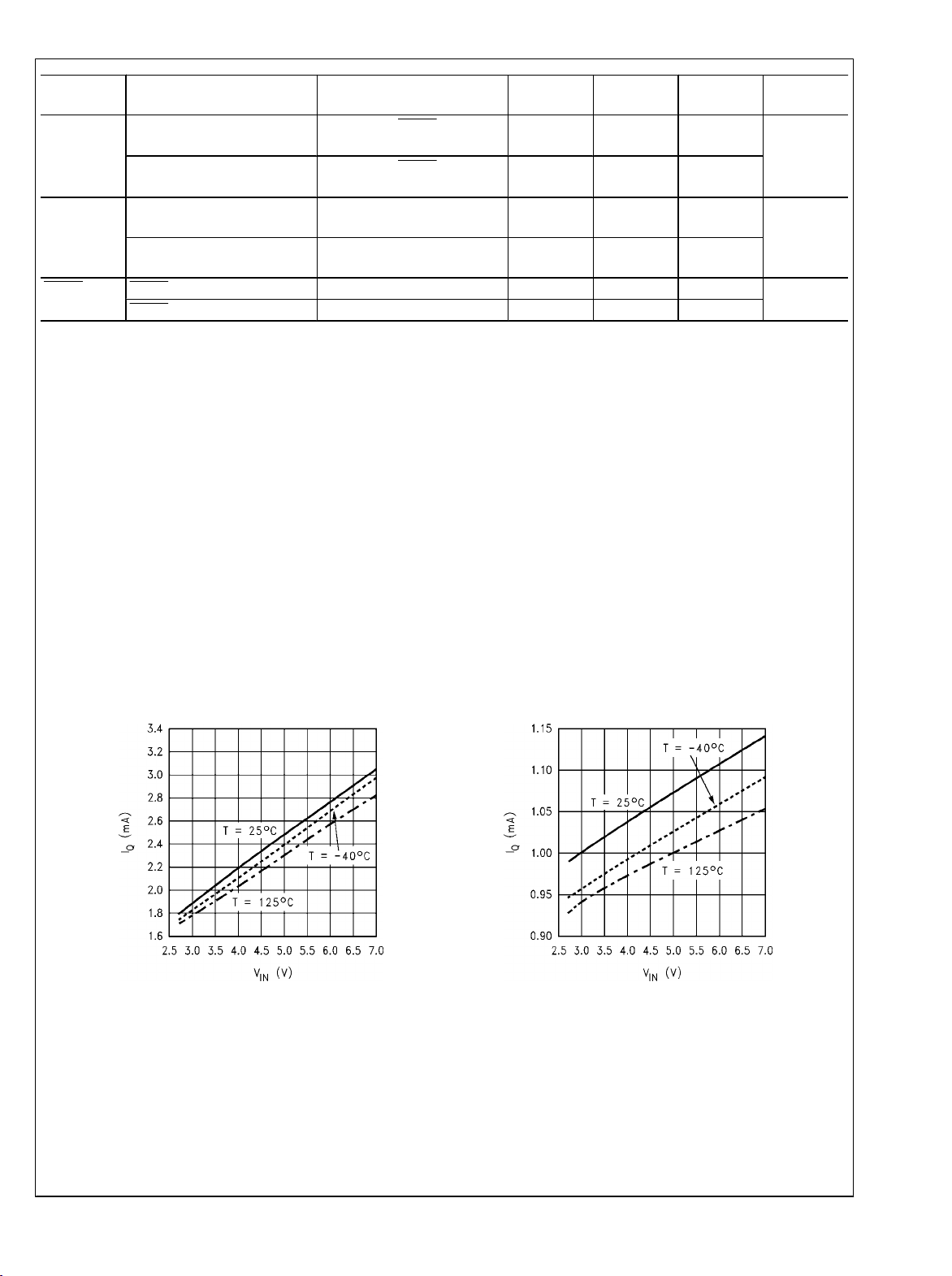
Typical Performance Characteristics
Switching Quiescent Current vs V
IN
20065755
Non-Switching Quiescent Current vs V
20065756
IN
5 www.national.com
LM3500
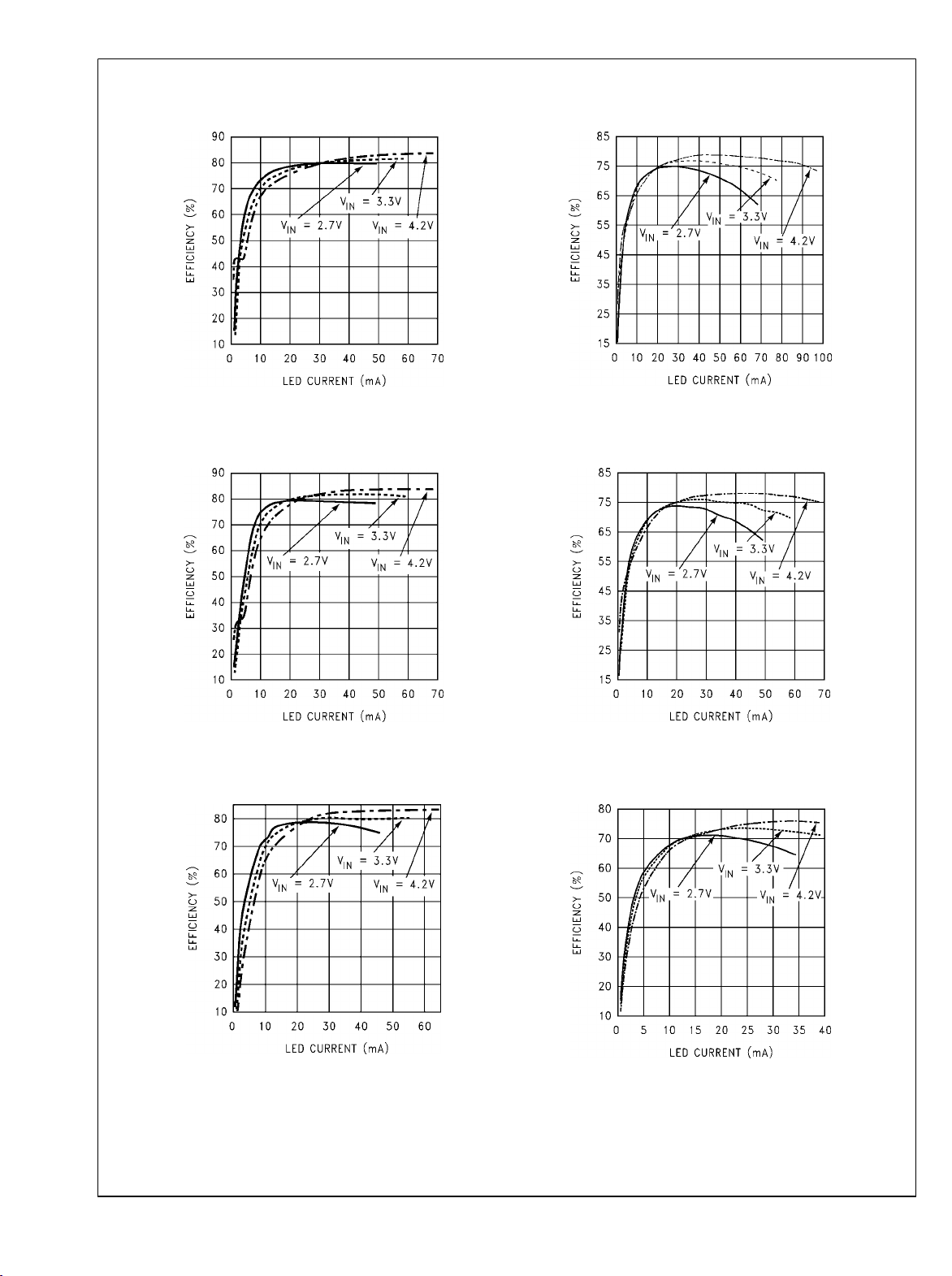
2 LED Efficiency vs LED Current
L = Coilcraft DT1608C-223,
Efficiency = 100*(PIN/(2V
LED*ILED
2 LED Efficiency vs LED Current
L = TDK VLP4612T-220MR34,
))
Efficiency = 100*(PIN/(2V
LED*ILED
))
3 LED Efficiency vs LED Current
L = Coilcraft DT1608C-223,
Efficiency = 100*(PIN/(3V
LED*ILED
4 LED Efficiency vs LED Current
L = Coilcraft DT1608C-223,
Efficiency = 100*(PIN/(4V
LED*ILED
20065757
))
20065758
))
3 LED Efficiency vs LED Current
L = TDK VLP4612T-220MR34,
Efficiency = 100*(PIN/(3V
LED*ILED
4 LED Efficiency vs LED Current
L = TDK VLP4612T-220MR34,
Efficiency = 100*(PIN/(4V
LED*ILED
20065779
))
20065780
))
20065759
www.national.com 6
20065781
 Loading...