

National LM2931AM-5.0, LM2931M-5.0 Schematic [ru]
LM2931
Series Low Dropout Regulators
LM2931 Series Low Dropout Regulators
November 2000
General Description
The LM2931 positive voltage regulator features a very low
quiescent current of 1mA or less when supplying 10mA
loads. This unique characteristic and the extremely low
input-output differential required for proper regulation (0.2V
for output currents of 10mA) make the LM2931 the ideal
regulator for standby power systems. Applications include
memory standby circuits, CMOS and other low power processor power supplies as well as systems demanding as
much as 100mA of output current.
Designed originally for automotive applications, the LM2931
and all regulated circuitry are protected from reverse battery
installations or 2 battery jumps. During line transients, such
as a load dump (60V) when the input voltage to the regulator
can momentarily exceed the specified maximum operating
voltage, the regulator will automatically shut down to protect
both internal circuits and the load. The LM2931 cannot be
harmed by temporary mirror-image insertion. Familiar regulator features such as short circuit and thermal overload
protection are also provided.
The LM2931 family includes a fixed 5V output (
ance for A grade) or an adjustable output with ON/OFF pin.
±
3.8% toler-
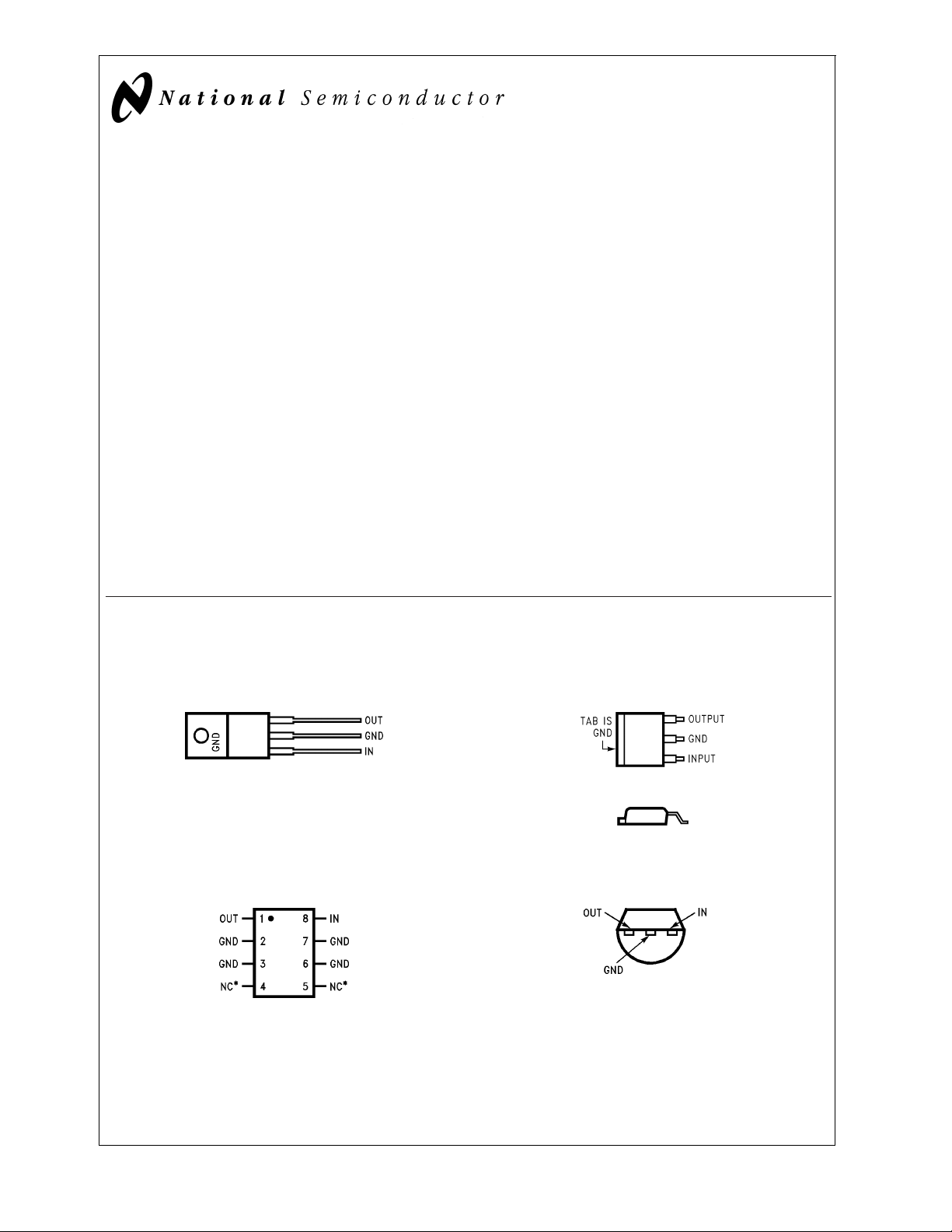
Connection Diagrams
FIXED VOLTAGE OUTPUT
Both versions are available in a TO-220 power package,
TO-263 surface mount package, and an 8-lead surface
mount package. The fixed output version is also available in
the TO-92 plastic and 6-Bump micro SMD packages.
Features
n Very low quiescent current
n Output current in excess of 100 mA
n Input-output differential less than 0.6V
n Reverse battery protection
n 60V load dump protection
n −50V reverse transient protection
n Short circuit protection
n Internal thermal overload protection
n Mirror-image insertion protection
n Available in TO-220, TO-92, TO-263, SO-8 or 6-Bump
micro SMD packages
n Available as adjustable with TTL compatible switch
n See AN-1112 for micro SMD considerations
TO-220 3-Lead Power Package
DS005254-6
Front View
8-Pin Surface Mount
DS005254-7
*NC = Not internally connected. Must be electrically isolated from the rest
of the circuit for the micro SMD package.
Top View
TO-263 Surface-Mount Package
DS005254-11
Top View
DS005254-12
Side View
TO-92 Plastic Package
DS005254-8
Bottom View
© 2000 National Semiconductor Corporation DS005254 www.national.com
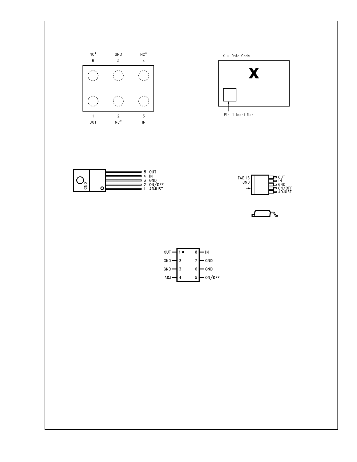
Connection Diagrams (Continued)
LM2931
6-Bump micro SMD
Top View
(Bump Side Down)
ADJUSTABLE OUTPUT VOLTAGE
micro SMD Laser Mark
DS005254-39
DS005254-38
TO-220 5-Lead Power Package
DS005254-9
Front View
TO-263
5-Lead Surface-Mount Package
DS005254-13
Top View
DS005254-14
Side View
8-Pin Surface Mount
DS005254-10
Top View
www.national.com 2
Connection Diagrams (Continued)
Ordering Information
LM2931
Output
Number
5V 3-Pin TO-220 LM2931T-5.0 LM2931T-5.0 Rails T03B
Adjustable,
3V to 24V
3.3V
Note: The micro SMD package marking is a single digit manufacturing Date Code Only.
Package Part Number Package Marking Transport Media NSC
Drawing
LM2931AT-5.0 LM2931AT-5.0 Rails
3-Pin TO-263 LM2931S-5.0 LM2931S-5.0 Rails TS3B
LM2931AS-5.0 LM2931AS-5.0 Rails
TO-92 LM2931Z-5.0 LM2931Z-5 1.8k Units per Box Z03A
LM2931AZ-5.0 LM2931AZ 1.8k Units per Box
8-Pin
SOIC
*
6-Bump
micro SMD
5-Pin TO-220 LM2931CT LM2931CT Rails T05A
5-Pin TO-263 LM2931CS LM2931CS Rails TS5B
8-Pin
SOIC
*
6-Bump
micro SMD
LM2931M-5.0 2931M-5.0 Rails M08A
LM2931AM-5.0 2931AM-5.0 Rails
LM2931IBPX-5.0 - Tape and Reel BPA06HTA
LM2931CM LM2931CM Rails M08A
LM2931IBPX-3.3 - Tape and Reel BPA06HTB
www.national.com3
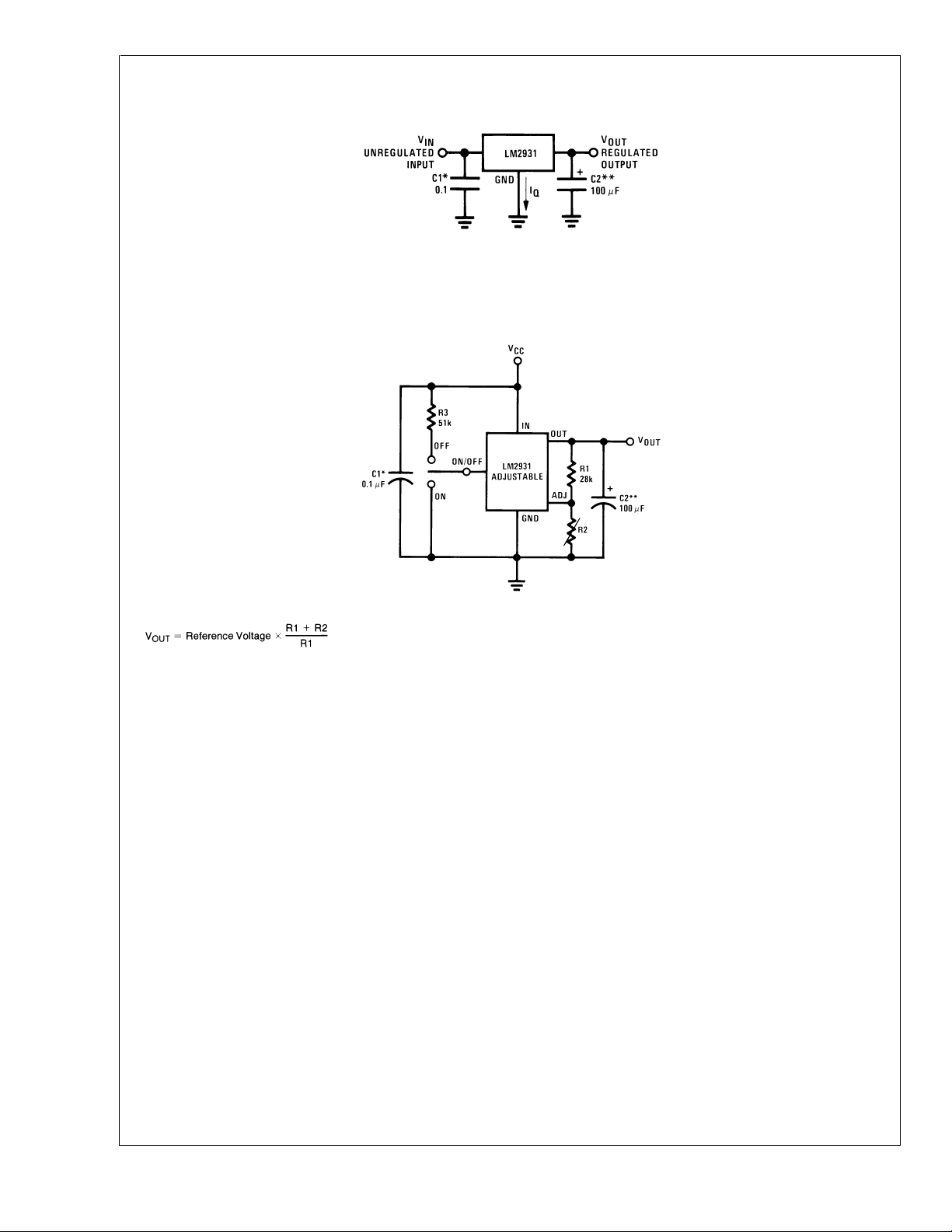
Typical Applications
LM2931
*
Required if regulator is located far from power supply filter.
*
*C2 must be at least 100 µF to maintain stability. May be increased without bound to maintain regulation during transients. Locate as close as possible to the
regulator. This capacitor must be rated over the same operating temperature range as the regulator. The equivalent series resistance (ESR) of this capacitor is
critical; see curve.
LM2931 Fixed Output
DS005254-4
LM2931 Adjustable Output
Note: Using 27k for R1 will automatically compensate for errors in V
DS005254-5
due to the input bias current of the ADJ pin (approximately 1 µA).
OUT
www.national.com 4
LM2931
Absolute Maximum Ratings (Note 1)
If Military/Aerospace specified devices are required,
please contact the National Semiconductor Sales Office/
Distributors for availability and specifications.
Input Voltage
Operating Range 26V
Overvoltage Protection
LM2931A, LM2931C (Adjustable) 60V
Internal Power Dissipation
(Note 2) (Note 4) Internally Limited
Operating Ambient Temperature
Range −40˚C to +85˚C
Maximum Junction Temperature 125˚C
Storage Temperature Range −65˚C to +150˚C
Lead Temp. (Soldering, 10 seconds) 230˚C
ESD Tolerance (Note 5) 2000V
LM2931 50V
Electrical Characteristics for Fixed 3.3V Version
VIN= 14V, IO= 10mA, TJ= 25˚C, C2= 100µF (unless otherwise specified) (Note 2)
Parameter Conditions LM2931-3.3 Units
Typ Limit
Output Voltage 3.3 3.465
4V ≤ VIN≤ 26V, IO= 100 mA
−40˚C ≤ T
≤ 125˚C
J
Line Regulation 4V ≤ VIN≤ 26V 4 33 mV
Load Regulation 5mA ≤ IO≤ 100mA 10 50 mV
Output Impedance 100mADCand 10mA
rms
,
200 mΩ
100Hz - 10kHz
Quiescent Current I
≤ 10mA, 4V ≤ VIN≤ 26V 0.4 1.0 mA
O
−40˚C ≤ TJ≤ 125˚C
I
= 100mA, VIN= 14V, TJ= 25˚C 15 mA
O
Output Noise Voltage 10Hz -100kHz, C
= 100µF 330 µV
OUT
Long Term Stability 13 mV/1000 hr
Ripple Rejection f
Dropout Voltage I
Maximum Operational
= 120Hz 80 dB
O
= 10mA
O
= 100mA
I
O
0.05
0.30
33 26 V
Input Voltage
Maximum Line Transient RL= 500Ω,VO≤5.5V,
70 50 V
T = 1ms, τ≤100ms
Reverse Polarity Input
VO≥ −0.3V, RL= 500Ω −30 −15 V
Voltage, DC
Reverse Polarity Input
T = 1ms, τ≤100ms, RL= 500Ω −80 −50 V
Voltage, Transient
(Note 3)
3.135
3.630
2.970
0.2
0.6
V
MAX
V
MIN
V
MAX
V
MIN
MAX
MAX
MAX
rms
V
MAX
MIN
MIN
MIN
MIN
Electrical Characteristics for Fixed 5V Version
VIN= 14V, IO= 10mA, TJ= 25˚C, C2 = 100 µF (unless otherwise specified) (Note 2)
Parameter Conditions LM2931A-5.0 LM2931-5.0 Units
Typ
Output Voltage 5 5.19
Limit
(Note 3)
Typ
5 5.25
4.81
6.0V ≤ VIN≤ 26V, IO= 100mA
−40˚C ≤ T
≤ 125˚C
J
Line Regulation 9V ≤ VIN≤ 16V
IN
≤ 26V
6V ≤ V
2
4
5.25
4.75
10
30
2
4
Load Regulation 5 mA ≤ IO≤ 100mA 14 50 14 50 mV
Output Impedance 100mADCand 10mA
rms
,
200 200 mΩ
100Hz -10kHz
Limit
(Note 3)
4.75
5.5
4.5
10
30
V
V
mV
www.national.com5
MAX
V
MIN
MAX
V
MIN
MAX
MAX
Electrical Characteristics for Fixed 5V Version (Continued)
VIN= 14V, IO= 10mA, TJ= 25˚C, C2 = 100 µF (unless otherwise specified) (Note 2)
LM2931
Parameter Conditions LM2931A-5.0 LM2931-5.0 Units
Limit
(Note 3)
Typ
Quiescent Current I
Typ
≤ 10mA, 6V ≤ VIN≤ 26V 0.4 1.0 0.4 1.0 mA
O
−40˚C ≤ TJ≤ 125˚C
I
= 100mA, VIN= 14V, TJ= 25˚C 15 30
O
15 mA
5
Output Noise Voltage 10Hz -100kHz, C
= 100µF 500 500 µV
OUT
Long Term Stability 20 20 mV/1000
Ripple Rejection f
Dropout Voltage IO= 10mA
Maximum Operational Input
= 120 Hz 80 55 80 dB
O
= 100mA
I
O
0.05
0.3
0.2
0.6
0.05
0.3
33 26 33 26 V
Voltage
Maximum Line Transient RL= 500Ω,VO≤5.5V,
T = 1ms, τ≤100ms
Reverse Polarity Input
VO≥ −0.3V, RL= 500Ω −30 −15 −30 −15 V
70 60 70 50 V
Voltage, DC
Reverse Polarity Input
T = 1ms, τ≤100ms, RL= 500Ω −80 −50 −80 −50 V
Voltage, Transient
Note 1: Absolute Maximum Ratings indicate limits beyond which damage to the device may occur. Electrical specifications do not apply when operating the device
beyond its rated operating conditions.
Note 2: See circuit in Typical Applications. To ensure constant junction temperature, low duty cycle pulse testing is used.
Note 3: All limits are guaranteed for T
Note 4: The maximum power dissipation is a function of maximum junction temperature T
maximum allowable power dissipation at anyambienttemperatureisP
and the LM2931 will go into thermal shutdown. For the LM2931 in the TO-92 package, θ
package, θ
sink, θ
If the TO-263 package is used, the thermal resistance can be reduced by increasing the P.C.board copper area thermally connected to the package: Using 0.5 square
inches of copper area, θ
Note 5: Human body model, 100 pF discharged through 1.5 kΩ.
is 50˚C/W; in the TO-263 package, θJAis 73˚C/W; and in the 6-Bump micro SMD package θJAis 290˚C/W. If the TO-220 package is used with a heat
JA
is the sum of the package thermal resistance junction-to-case of 3˚C/W and the thermal resistance added by the heat sink and thermal interface.
JA
is 50˚C/W; with 1 square inch of copper area, θJAis 37˚C/W; and with 1.6 or more square inches of copper area, θJAis 32˚C/W.
JA
= 25˚C (standard type face) or over the full operating junction temperature range of −40˚C to +125˚C (bold type face).
J
D
=(T
)/θJA. If this dissipation is exceeded, the die temperature will rise above 150˚C
Jmax−TA
, total thermal resistance θJA, and ambient temperature TA. The
Jmax
is 195˚C/W; in the SO-8 package, θJAis 160˚C/W, and in the TO-220
JA
Limit
(Note 3)
0.2
0.6
mA
V
MAX
MAX
MIN
rms
hr
MIN
MAX
MIN
MIN
MIN
MIN
Electrical Characteristics for Adjustable Version
VIN= 14V, V
Reference Voltage 1.20 1.26 V
Output Voltage Range 24 V
Line Regulation V
Load Regulation 5 mA ≤ IO≤ 100 mA 0.3 1 %
Output Impedance 100 mADCand 10 mA
Quiescent Current I
Output Noise Voltage 10 Hz–100 kHz 100 µV
Long Term Stability 0.4 %/1000 hr
Ripple Rejection f
www.national.com 6
= 3V, IO= 10 mA, TJ= 25˚C, R1 = 27k, C2 = 100 µF (unless otherwise specified) (Note 2)
OUT
Parameter Conditions Typ Limit Units
Limit
MAX
1.14 V
IO≤ 100 mA, −40˚C ≤ Tj≤ 125˚C, R1 = 27k 1.32 V
Measured from V
to Adjust Pin 1.08 V
OUT
3V
+ 0.6V ≤ VIN≤ 26V 0.2 1.5 mV/V
OUT
, 100 Hz–10 kHz 40 mΩ/V
rms
= 10 mA 0.4 1 mA
O
MIN
MAX
MIN
MAX
MIN
MAX
IO= 100 mA 15 mA
During Shutdown R
= 120 Hz 0.02 %/V
O
= 500Ω 0.8 1 mA
L
rms
MAX
MAX
MAX
/V
 Loading...