

National LM2760M5 Schematic [ru]
December 2002
LM2760
3.3V Regulated Switched Capacitor Voltage Converter
LM2760 3.3V Regulated Switched Capacitor Voltage Converter
General Description
The LM2760 is a switched-capacitor DC/DC converter that
generates a regulated 3.3V output capable of driving a load
up to 20mA (V
(2.0V-4.4V) allows this device to be powered from several
types of batteries, including single cell lithium-ion, two-cell
alkaline, nickel-metal-hydride, and nickel-cadmium. The
LM2760 solution does not require an inductor and needs
only three small external ceramic capacitors. The miniscule
quiescent current of the part, typically 10µA unloaded,
makes the LM2760 ideal for low-current standby power rails.
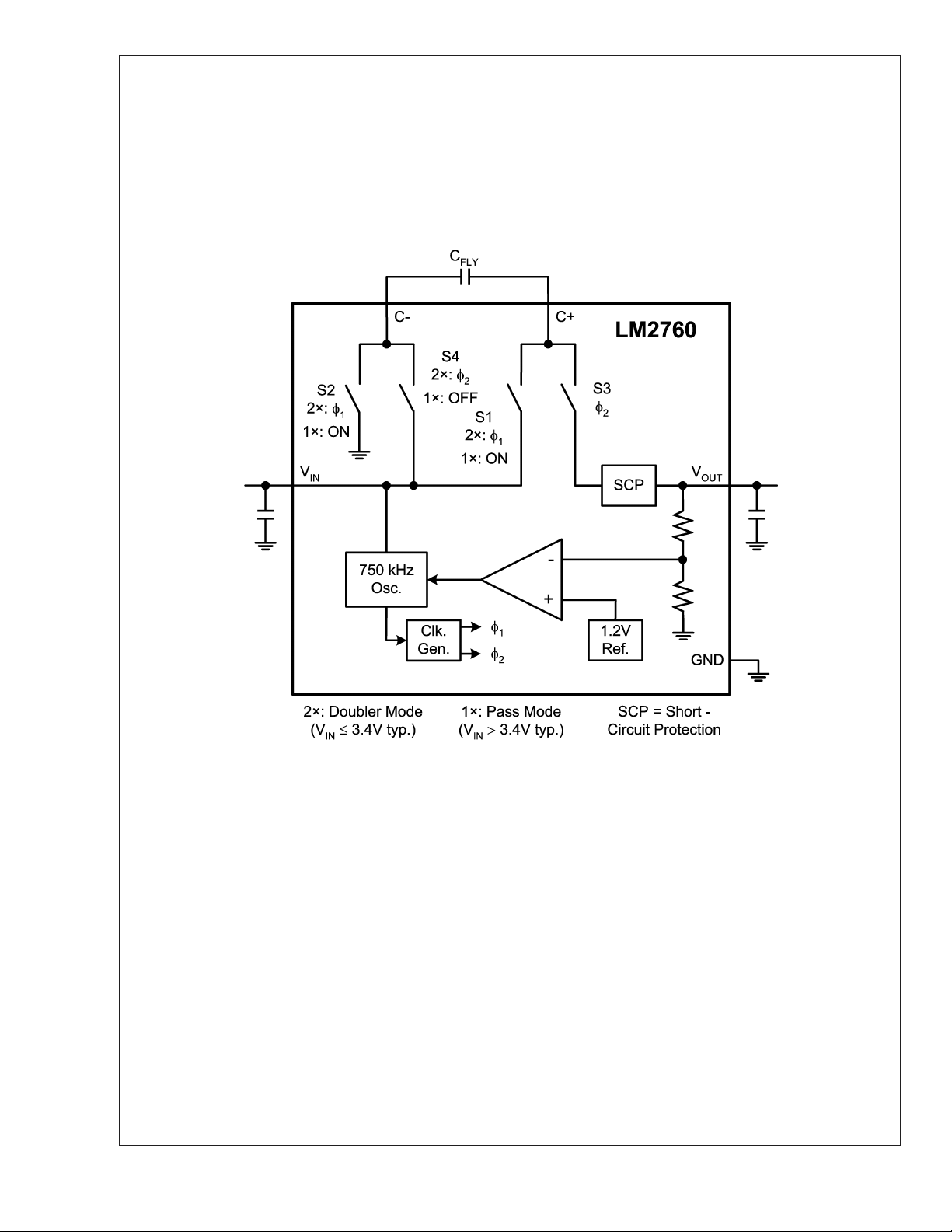
The LM2760 is a switched-capacitor circuit that is controlled
by a gated oscillator. Both a low-input-voltage boost mode
and high-input-voltage pass mode are implemented to optimize efficiency over the full input voltage range.
Additional features of the LM2760 include thermal protection
and current limiting. The LM2760 is available in a small,
five-pin SOT-23 package.
≥ 2.5V). The wide input voltage range
IN
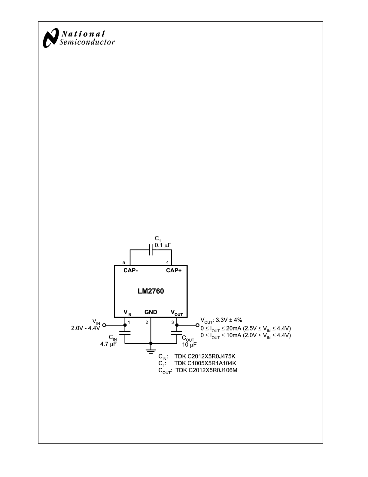
Typical Application Circuit
Features
n 3.3V±4% Regulated Output
n Ultralow Power: 10µA Typical Supply Current
n Boost and Pass Modes for Improved Efficiency
n Input Voltage Range: 2.0V to 4.4V
n Output Current up to 20mA (V
n Output Current up to 10mA (V
n Inductorless solution
n Small external parts count: 3 ceramic capacitors
n 750kHz Switching Frequency
n SOT23-5 Package
n Short-Circuit and Thermal Protection
≥ 2.5V)
IN
≥ 2.0V)
IN
Applications
n Battery-Operated Devices
n Cellular Phone
n Standby Power Supply
n Memory Keep-alive Power
20044301
© 2002 National Semiconductor Corporation DS200443 www.national.com
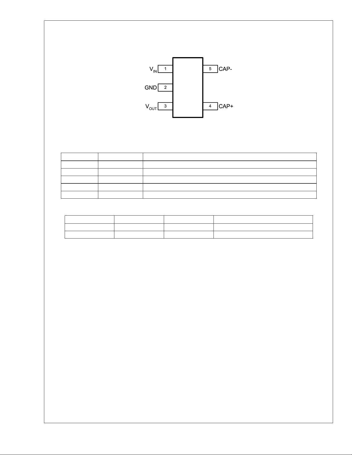
Connection Diagram
LM2760
LM2760
SOT23-5 Package
NS Package Number MF05A
Pin Description
Pin #(s) Pin Name Description
1V
2 GND Ground connection
3V
4 CAP+ Charge pump capacitor (+) connection
5 CAP- Charge pump capacitor (-) connnection
IN
OUT
Ordering Information
Order # Package Type Package Marking Supplied as
LM2760M5 SOT23-5 S19B Rail (250 units/rail)
LM2760M5X SOT23-5 S19B Tape and reel (3000 units/reel)
Top View
20044302
Input supply connection
Regulated 3.3V output
www.national.com 2
LM2760
Absolute Maximum Ratings (Notes 1,
2)
If Military/Aerospace specified devices are required,
please contact the National Semiconductor Sales Office/
Distributors for availability and specifications.
Pin: Voltage to GND −0.3V to 6V
V
IN
Junction Temperature (T
J-MAX-ABS
Continuous Power Dissipation Internally Limited
) 150˚C
Operating Ratings (Notes 1, 2)
Input Voltage Range 2.0V to 4.4V
Recommended Output Current
2.5V ≤ V
2.0V ≤ V
Junction Temperature (T
Ambient Temperature (T
(Note 6)
≤ 4.4V 0mA to 20mA
IN
≤ 2.5V 0mA to 10mA
IN
) Range -40˚C to 100˚C
J
) Range
A
-40˚C to 85˚C
(Note 3)
V
Short-Circuit to GND Duration Unlimited
OUT
(Note 4)
Thermal Information
Storage Temperature Range -65˚C to 150˚C
Lead Temperature 260˚C
(Soldering, 5 sec.)
ESD Rating (Note 5)
Human-body model:
Machine model
2kV
200 V
Junction-to-Ambient Thermal 220˚C/W
Resistance (θ
), SOT23-5
JA
Package(Note 7)
Electrical Characteristics (Notes 2, 8)
Typical values and limits in standard typeface apply for TJ=25oC. Limits in boldface type apply over the operating junction
temperature range 0
= 10µF(Note 10)
C
OUT
Symbol Parameter Conditions Min Typ Max Units
V
OUT
I
Q
I
IN
f
OSC
V
p-p
t
ON
I
SC
Note 1: Absolute Maximum Ratings indicate limits beyond which damage to the component may occur. Operating Ratings are conditions under which operation of
the device is guaranteed. Operating Ratings do not imply guaranteed performance limits. For guaranteed performance limits and associated test conditions, see the
Electrical Characteristics tables.
Note 2: All voltages are with respect to the potential at the GND pin.
Note 3: Thermal shutdown circuitry protects the device from permanent damage.
Note 4: Excessive power dissipation will occur if the part is shorted to ground. Internal thermal shutdown will protect the device from permanent damage, but
thermal cycling of the part is likely to occur until the short is removed. Protection is guaranteed only for V
Note 5: : The human-body model is a 100 pF capacitor discharged through a 1.5 kΩ resistor into each pin. The machine model is a 200pF capacitor discharged
directly into each pin.
Note 6: Maximum ambient temperature (T
dissipation of the device in the application (P
following equation: T
LM2760 is 70mW. This occurs when the output current is 20mA and the input voltage is 3.4V (edge of the "doubler" region). The maximum ambient temperature
operating rating (T
Dissipation section of this datasheet.
Note 7: Junction-to-ambient thermal resistance (θ
guidelines set forth in the JEDEC standard JESD51-3. The test board is a 2-layer FR-4 board measuring 230mm x 125mm x 1.6mm. Thickness of the copper layers
is 18mm (1.0oz). Ambient temperature in simulation is 22˚C, still air. Power dissipation is 1W. Junction-to-ambient thermal resistance is a highly application-specific
parameter. The value of θ
Note 8: : All room temperature limits are 100% tested or guaranteed through statistical analysis. All limits at temperature extremes are guaranteed by correlation
using standard Statistical Quality Control methods (SQC). All limits are used to calculate Average Outgoing Quality Level (AOQL). Typical numbers are not
guaranteed, but do represent the most likely norm.
Note 9: With P
o
the 0
Note 10: C
D-MAX
C-to-85oC junction temperature range that is used in determining guaranteed limits.
FLY,CIN
o
C≤ TJ≤ +85oC[0oC ≤ TA≤ +70oC (Note 9)] Unless otherwise specified: CIN= 4.7µF, C
Output Voltage 2.5V ≤ VIN≤ 4.4V,
OUT
IN
OUT
≤ 20mA
≤ 4.4V,
≤ 10mA
0mA ≤ I
2.0V ≤ V
0mA ≤ I
Quiescent Supply Current 2.0V ≤ VIN≤ 4.4V, V
OUT
tied to
3.17 3.3 3.43 V
3.17 3.3 3.43 V
6 12 µA
FLY
= 0.1µF,
3.5V, unloaded (Note 11)
Normal Operation Supply
Current
2.0V ≤ VIN≤ 4.4V, unloaded,
Time-averaged (Note 12)
10 µA
Oscillator Frequency VIN= 3.0V 750 kHz
Output Ripple Voltage VIN= 3.0V, I
V
Turn-On Time VIN= 3.0V (Note 13) 1 ms
OUT
= 10mA 60 mV
OUT
Output Short Circuit Current VIN= 3.0V 170 mA
≤ 4.4V
IN
) is dependent on the maximum operating junction temperature (T
A-MAX
), and the junction-to-ambient thermal resistance of the part/package in the application (θJA), as given by the
D-MAX
A-MAX=TJ-MAX-OP
)of85oC is calculated using θJA= 220oC/W and P
A-MAX
of the LM2760 could fall in a range as wide as 150oC/W to 250oC/W (if not wider), depending on PCB and application conditions.
JA
of 70mW and θJAof 220oC/W (see Note 6), the ambient temperature range of 0oC-to-70oC is provided for convenience and is calculated from
, and C
OUT
-(θJAxP
: Low-ESR Surface-Mount Ceramic Capacitors (MLCCs) used in setting electrical characteristics
). When application conditions are within the specified operating ratings, maximum power dissipation of the
D-MAX
= 70mW. For more information on these topics, please refer to the Power
D-MAX
) of the SOT23-5 package is taken from a thermal modeling result, performed under the conditions and
JA
= 100oC), the maximum power
J-MAX-OP
p-p
www.national.com3
Electrical Characteristics (Notes 2, 8) (Continued)
Note 11: In determining quiescent supply current limits, the voltage on the V
LM2760
inactive and all internal switches are off.
Note 12: The "normal operation" supply current specification is a measure of the time-averaged supply current when there is no current load connected to the output
of the LM2760. During this so-called normal operation, the charge pump occasionally is activated to provide charge to the output cap and keep the output voltage
from drooping. This is necessary because, when the pump is not active, the output capacitor supplies current to the internal feedback resistor divider. The occasional
pumping typically occurs every 2 seconds on average, contains a few short pump cycles, and results in a small increase in the average quiescent supply current.
Note 13: Turn-on time is measured from when the input voltage (V
) is established until the output voltage crosses 90% of its final value.
IN
pin is forced to 200mV above the typical V
OUT
to ensure that the charge pump is
OUT
Block Diagram
www.national.com 4
20044303
 Loading...