

National LM2733XMF, LM2733YMF Schematic [ru]
February 2003
LM2733
0.6/1.6 MHz Boost Converters With 40V Internal FET
Switch in SOT-23
LM2733 0.6/1.6 MHz Boost Converters With 40V Internal FET Switch in SOT-23
General Description
The LM2733 switching regulators are current-mode boost
converters operating fixed frequency of 1.6 MHz (“X” option)
and 600 kHz (“Y” option).
The use of SOT-23 package, made possible by the minimal
power loss of the internal 1A switch, and use of small inductors and capacitors result in the industry’s highest power
density. The 40V internal switch makes these solutions perfect for boosting to voltages of 16V or greater.
These parts have a logic-level shutdown pin that can be
used to reduce quiescent current and extend battery life.
Protection is provided through cycle-by-cycle current limiting
and thermal shutdown. Internal compensation simplifies design and reduces component count.
Switch Frequency
XY
1.6 MHz 0.6 MHz
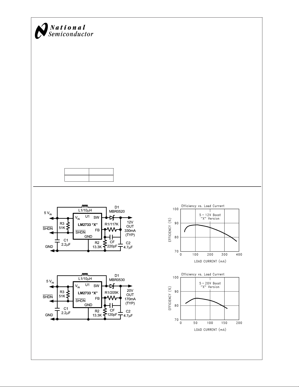
Typical Application Circuit
Features
n 40V DMOS FET switch
n 1.6 MHz (“X”), 0.6 MHz (“Y”) switching frequency
n Low R
n Switch current up to 1A
n Wide input voltage range (2.7V–14V)
n Low shutdown current (
n 5-Lead SOT-23 package
n Uses tiny capacitors and inductors
n Cycle-by-cycle current limiting
n Internally compensated
(ON) DMOS FET
DS
<
1 µA)
Applications
n White LED Current Source
n PDA’s and Palm-Top Computers
n Digital Cameras
n Portable Phones and Games
n Local Boost Regulator
20055424
20055457
20055401
20055458
© 2003 National Semiconductor Corporation DS200554 www.national.com
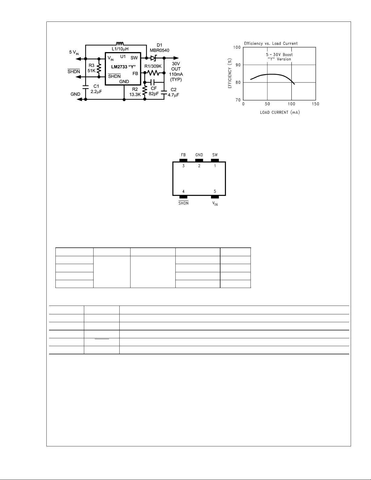
Typical Application Circuit (Continued)
LM2733
Connection Diagram
20055440
20055459
Top View
5-Lead SOT-23 Package
See NS Package Number MF05A
20055402
Ordering Information
Order Number Package Type Package Drawing Supplied As Package ID
LM2733XMF
LM2733XMFX 3K Tape and Reel S52A
LM2733YMF 1K Tape and Reel S52B
LM2733YMFX 3K Tape and Reel S52B
SOT23-5 MF05A
1K Tape and Reel S52A
Pin Description
Pin Name Function
1 SW Drain of the internal FET switch.
2 GND Analog and power ground.
3 FB Feedback point that connects to external resistive divider.
4 SHDN
5V
IN
Shutdown control input. Connect to VINif this feature is not used.
Analog and power input.
www.national.com 2
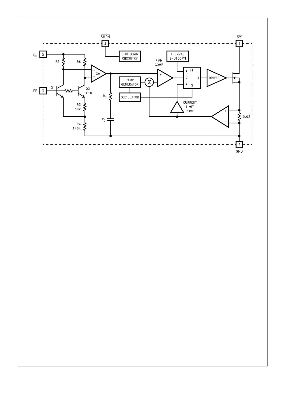
Block Diagram
LM2733
20055403
Theory of Operation
The LM2733 is a switching converter IC that operates at a
fixed frequency (0.6 or 1.6 MHz) using current-mode control
for fast transient response over a wide input voltage range
and incorporate pulse-by-pulse current limiting protection.
Because this is current mode control, a 50 mΩ sense resistor in series with the switch FET is used to provide a voltage
(which is proportional to the FET current) to both the input of
the pulse width modulation (PWM) comparator and the current limit amplifier.
At the beginning of each cycle, the S-R latch turns on the
FET. As the current through the FET increases, a voltage
(proportional to this current) is summed with the ramp coming from the ramp generator and then fed into the input of the
PWM comparator. When this voltage exceeds the voltage on
the other input (coming from the Gm amplifier), the latch
resets and turns the FET off. Since the signal coming from
the Gm amplifier is derived from the feedback (which
samples the voltage at the output), the action of the PWM
comparator constantly sets the correct peak current through
the FET to keep the output volatge in regulation.
Q1 and Q2 along with R3 - R6 form a bandgap voltage
reference used by the IC to hold the output in regulation. The
currents flowing through Q1 and Q2 will be equal, and the
feedback loop will adjust the regulated output to maintain
this. Because of this, the regulated output is always maintained at a voltage level equal to the voltage at the FB node
"multiplied up" by the ratio of the output resistive divider.
The current limit comparator feeds directly into the flip-flop,
that drives the switch FET. If the FET current reaches the
limit threshold, the FET is turned off and the cycle terminated
until the next clock pulse. The current limit input terminates
the pulse regardless of the status of the output of the PWM
comparator.
www.national.com3
Absolute Maximum Ratings (Note 1)
If Military/Aerospace specified devices are required,
LM2733
please contact the National Semiconductor Sales Office/
Distributors for availability and specifications.
Storage Temperature Range −65˚C to +150˚C
Operating Junction
Temperature Range −40˚C to +125˚C
Lead Temp. (Soldering, 5 sec.) 300˚C
Power Dissipation (Note 2) Internally Limited
FB Pin Voltage −0.4V to +6V
SW Pin Voltage −0.4V to +40V
Input Supply Voltage −0.4V to +14.5V
Shutdown Input Voltage
(Survival) −0.4V to +14.5V
θ
(SOT23-5) 265˚C/W
J-A
ESD Rating (Note 3)
Human Body Model
Machine Model
Electrical Characteristics
Limits in standard typeface are for TJ= 25˚C, and limits in boldface type apply over the full operating temperature range
(−40˚C ≤ T
≤ +125˚C). Unless otherwise specified: VIN= 5V, V
J
Symbol Parameter Conditions
V
IN
I
SW
R
(ON) Switch ON Resistance ISW= 100 mA 500 650 mΩ
DS
SHDN
Input Voltage 2.7 14 V
Switch Current Limit (Note 6) 1.0 1.5 A
Shutdown Threshold Device ON 1.5
TH
Device OFF 0.50
I
SHDN
V
FB
Shutdown Pin Bias Current V
Feedback Pin Reference
=0 0
SHDN
V
=5V 0 2
SHDN
VIN=3V
Voltage
I
FB
I
Q
Feedback Pin Bias Current VFB= 1.23V 60 nA
Quiescent Current V
= 5V, Switching "X" 2.1 3.0
SHDN
V
= 5V, Switching "Y" 1.1 2
SHDN
V
= 5V, Not Switching 400 500
SHDN
V
= 0 0.024 1
SHDN
FB Voltage Line Regulation 2.7V ≤ VIN≤ 14V
= 5V, IL= 0A.
SHDN
Min
(Note 4)
Typical
(Note 5)
Max
(Note 4)
1.205 1.230 1.255 V
0.02 %/V
2kV
200V
Units
V
µA
mA
µA
F
SW
Switching Frequency “X” Option 1.15 1.6 1.85
“Y” Option 0.40 0.60 0.8
D
MAX
Maximum Duty Cycle “X” Option 87 93
“Y” Option 93 96
I
L
Note 1: Absolute Maximum Ratings indicate limits beyond which damage to the component may occur. Electrical specifications do not apply when operating the
device outside of the limits set forth under the operating ratings which specify the intended range of operating conditions.
Note 2: The maximum power dissipation which can be safely dissipated for any application is a function of the maximum junction temperature, T
the junction-to-ambient thermal resistance for the SOT-23 package, θ
at any ambient temperature for designs using this device can be calculated using the formula:
If power dissipation exceeds the maximum specified above, the internal thermal protection circuitry will protect the device by reducing the output voltage as required
to maintain a safe junction temperature.
Note 3: The human body model is a 100 pF capacitor discharged through a 1.5 kΩ resistor into each pin. The machine model is a 200 pF capacitor discharged
directly into each pin.
Note 4: Limits are guaranteed by testing, statistical correlation, or design.
Note 5: Typical values are derived from the mean value of a large quantity of samples tested during characterization and represent the most likely expected value
of the parameter at room temperature.
Note 6: Switch current limit is dependent on duty cycle (see Typical Performance Characteristics). Limits shown are for duty cycles ≤ 50%.
www.national.com 4
Switch Leakage Not Switching VSW=5V 1 µA
(MAX) = 125˚C,
= 265˚C/W, and the ambient temperature, TA. The maximum allowable power dissipation
J-A
J
MHz
%
LM2733
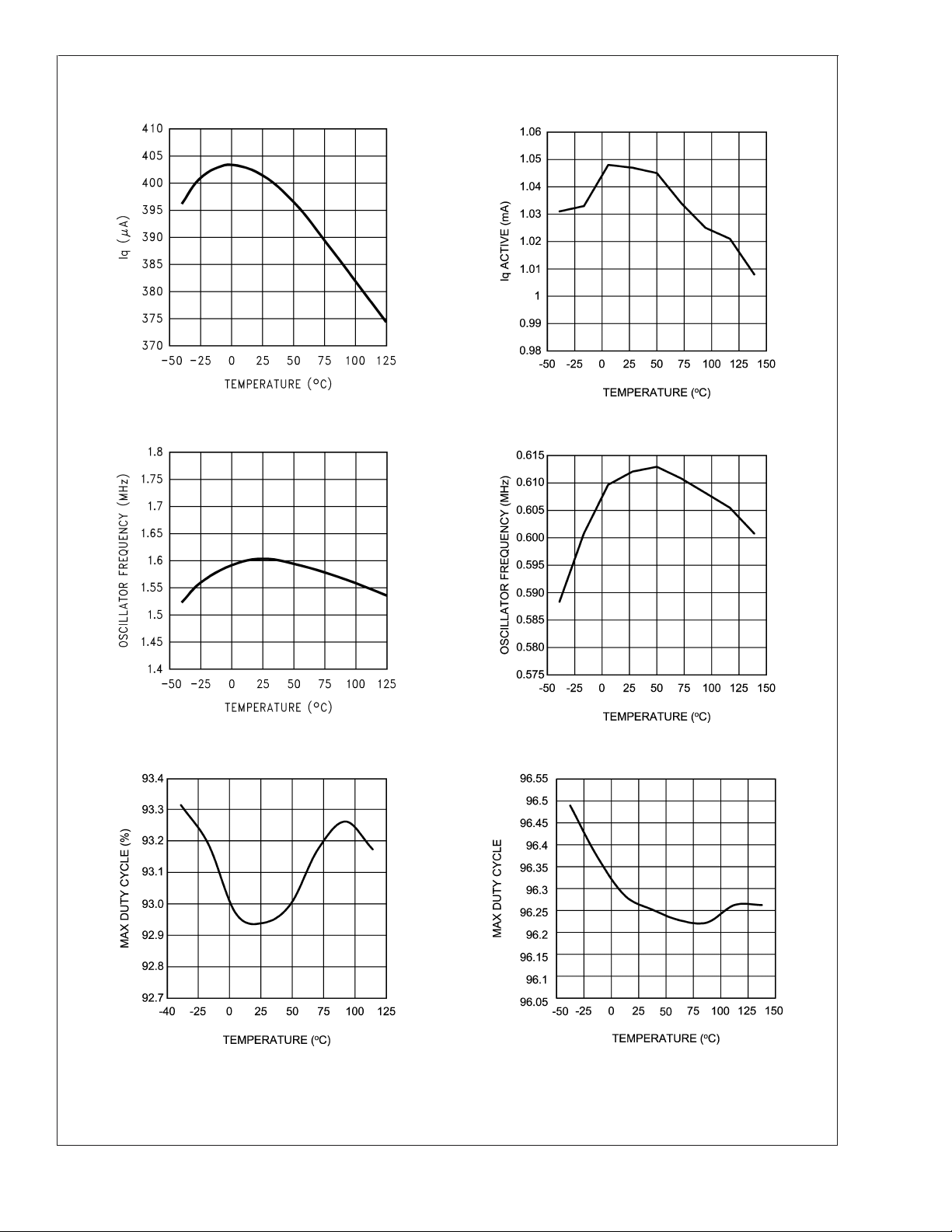
Typical Performance Characteristics Unless otherwise specified: V
(Active) vs Temperature - "X" Iq VIN(Active) vs Temperature - "Y"
Iq V
IN
20055410
= 5V, SHDN pin is tied to VIN.
IN
Oscillator Frequency vs Temperature - "X" Oscillator Frequency vs Temperature - "Y"
20055442
20055408
20055443
Max. Duty Cycle vs Temperature - "X" Max. Duty Cycle vs Temperature - "Y"
20055455
20055456
www.national.com5
 Loading...