

National LM2660MM, LM2661MM Schematic [ru]
LM2660/LM2661
Switched Capacitor Voltage Converter
LM2660/LM2661 Switched Capacitor Voltage Converter
September 1999
General Description
The LM2660/LM2661 CMOS charge-pump voltage converter inverts a positive voltage in the range of 1.5V to 5.5V
to the corresponding negative voltage. The LM2660/LM2661
uses two low cost capacitors to provide 100 mA of output
current without the cost, size, and EMI related to inductor
based converters. With an operating current of only 120 µA
and operating efficiency greater than 90% at most loads, the
LM2660/LM2661 provides ideal performance for battery
powered systems. The LM2660/LM2661 may also be used
as a positive voltage doubler.
The oscillator frequency can be lowered by adding an external capacitor to the OSC pin. Also, the OSC pin may be used
to drive the LM2660/LM2661 with an external clock. For
LM2660, a frequency control (FC) pin selects the oscillator
frequency of 10 kHz or 80 kHz. For LM2661, an external
shutdown (SD) pin replaces the FC pin. The SD pin can be
used to disable the device and reduce the quiescent current
to 0.5 µA. The oscillator frequency for the LM2661 is 80 kHz.
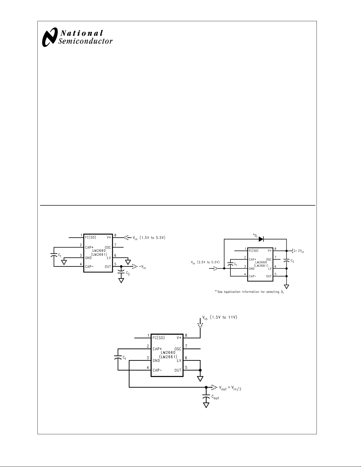
Basic Application Circuits
Voltage Inverter Positive Voltage Doubler
Features
n Inverts or doubles input supply voltage
n Narrow SO-8 and Mini SO-8 Package
n 6.5Ω typical output resistance
n 88% typical conversion efficiency at 100 mA
n (LM2660) selectable oscillator frequency: 10 kHz/80 kHz
n (LM2661) low current shutdown mode
Applications
n Laptop computers
n Cellular phones
n Medical instruments
n Operational amplifier power supplies
n Interface power supplies
n Handheld instruments
01291103
01291104
Splitting VINin Half
01291126
© 2004 National Semiconductor Corporation DS012911 www.national.com
Absolute Maximum Ratings (Note 1)
If Military/Aerospace specified devices are required,
please contact the National Semiconductor Sales Office/
Distributors for availability and specifications.
Supply Voltage (V+ to GND, or GND to OUT) 6V
LM2660/LM2661
LV (OUT − 0.3V) to (GND + 3V)
FC, OSC The least negative of (OUT −
0.3V) or (V+ − 6V) to (V+ + 0.3V)
V+ and OUT Continuous Output Current 120 mA
Output Short-Circuit Duration to GND (Note
2) 1 sec.
Power Dissipation
(T
= 25˚C) (Note 3) 735 mW 500 mW
A
T
Max (Note 3) 150˚C 150˚C
J
θ
(Note 3) 170˚C/W 250˚C/W
JA
Operating Junction
Temperature
Range −40˚C to +85˚C
Storage Temperature
Range
Package
MMM
−65˚C to +150˚C
Lead Temperature 300˚C
(Soldering, 10 seconds)
ESD Rating 2 kV
Electrical Characteristics
Limits in standard typeface are for TJ= 25˚C, and limits in boldface type apply over the full operating temperature range. Unless otherwise specified: V+ = 5V, FC = Open, C
Symbol Parameter Condition Min Typ Max Units
V+ Supply Voltage R
I
Q
I
SD
Supply Current No Load FC = Open (LM2660) 0.12 0.5
Shutdown Supply Current
L
(LM2661)
V
SD
Shutdown Pin Input Voltage Shutdown Mode 2.0 (Note 5)
(LM2661) Normal Operation 0.3
I
R
f
f
I
L
OUT
OSC
SW
OSC
Output Current TA≤ +85˚C, OUT ≤ −4V 100
T
A
Output Resistance (Note 6) IL= 100 mA TA≤ +85˚C 6.5 10
Oscillator Frequency (Note 7) OSC = Open FC = Open 5 10
Switching Frequency (Note 8) OSC = Open FC = Open 2.5 5
OSC Input Current FC = Open
FC=V+
P
EFF
V
OEFF
Note 1: Absolute maximum ratings indicate limits beyond which damage to the device may occur. Electrical specifications do not apply when operating the device
beyond its rated operating conditions.
Note 2: OUT may be shorted to GND for one second without damage. However, shorting OUT to V+ may damage the device and should be avoided. Also, for
temperatures above 85˚C, OUT must not be shorted to GND or V+, or device may be damaged.
Note 3: The maximum allowable power dissipation is calculated by using P
ambient temperature, and θ
Note 4: In the test circuit, capacitors C
voltage and efficiency.
Note 5: In doubling mode, when V
Note 6: Specified output resistance includes internal switch resistance and capacitor ESR.
Note 7: For LM2661, the oscillator frequency is 80 kHz.
Note 8: The output switches operate at one half of the oscillator frequency, f
Power Efficiency RL(1k) between V+and OUT 96 98
R
L
I
L
Voltage Conversion Efficiency No Load 99 99.96 %
is the junction-to-ambient thermal resistance of the specified package.
JA
and C2are 0.2Ω maximum ESR capacitors. Capacitors with higher ESR will increase output resistance, reduce output
1
>
5V, minimum input high for shutdown equals V
out
= 150 µF. (Note 4)
1=C2
= 1k Inverter, LV = Open 3.5 5.5
Inverter, LV = GND 1.5 5.5 V
Doubler, LV = OUT 2.5 5.5
SD = Ground (LM2661)
1 3
0.5 2 µA
>
+85˚C, OUT ≤ −3.8V 100
>
T
+85˚C 12
A
FC=V+ 40 80
FC=V+ 20 40
±
2
±
16
(500) between GND and OUT 92 96 %
= 100 mA to GND 88
DMax
OSC
=(T
=2fSW.
JMax−TA
−3V.
out
)/θJA, where T
is the maximum junction temperature, TAis the
JMax
mALV = Open FC = V+ (LM2660) or
V
mA
Ω
kHz
kHz
µA
www.national.com 2
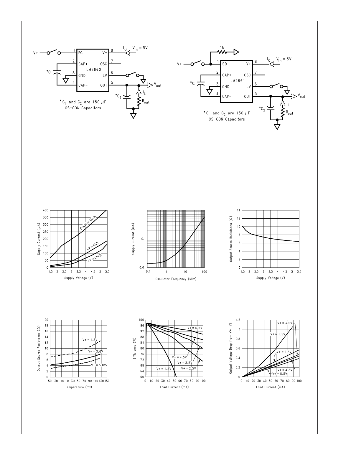
Test Circuits
01291105
FIGURE 1. LM2660 and LM2661 Test Circuits
Typical Performance Characteristics
(Circuit of Figure 1)
Supply Current vs
Supply Voltage
Supply Current vs
Oscillator Frequency
LM2660/LM2661
01291106
Output Source
Resistance vs Supply
Voltage
Output Source
Resistance vs
Temperature
01291107
01291110
Efficiency vs Load
Current
01291108
01291111
01291109
Output Voltage Drop
vs Load Current
01291112
www.national.com3
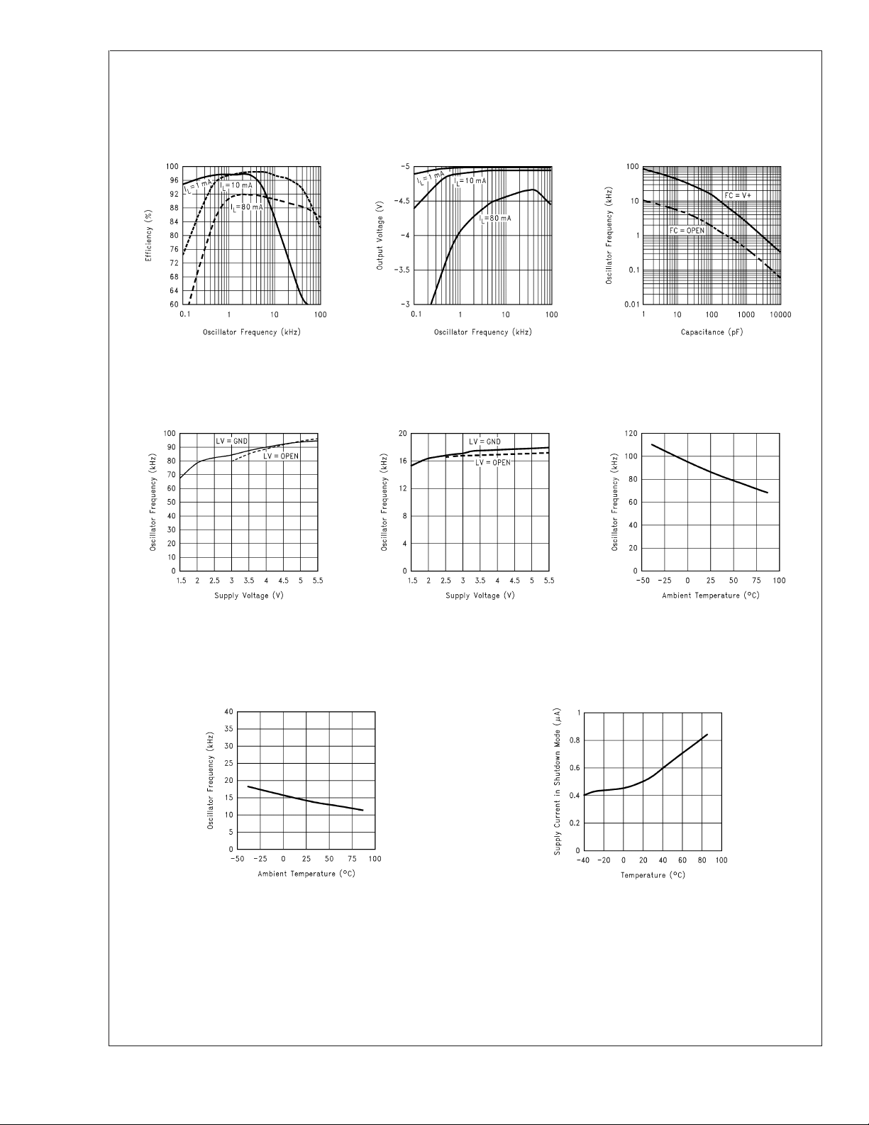
Typical Performance Characteristics (Circuit of Figure 1) (Continued)
Efficiency vs
Oscillator Frequency
LM2660/LM2661
01291113 01291114 01291115
Output Voltage vs
Oscillator Frequency
Oscillator Frequency
vs External
Capacitance
Oscillator Frequency
vs Supply Voltage
(FC = V+)
Oscillator Frequency
vs Temperature
(FC = Open)
Oscillator Frequency
vs Supply Voltage
(FC = Open)
01291116 01291117 01291118
Oscillator Frequency
vs Temperature
(FC = V+)
Shutdown Supply
Current vs
Temperature
(LM2661 Only)
01291119
www.national.com 4
01291120
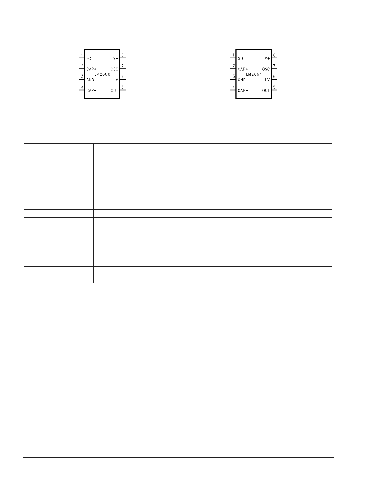
Connection Diagrams
8-Lead SO (M) or Mini SO (MM)
01291101 01291102
Top View
Order Number LM2660M, LM2661M, LM2660MM or LM2661MM
See NS Package Number M08A and MUA08A
Ordering Information
Order Number Package Number Package Marking Supplied As
LM2660M M08A Datecode Rail (95 units/rail)
LM26
60M
LM2660MX M08A Datecode Tape and Reel (2500 units/rail)
LM26
60M
LM2660MM MUA08A S01A (Note 9) Tape and Reel (250 units/rail)
LM2660MMX MUA08A S01A (Note 9) Tape and Reel (3500 units/rail)
LM2661M M08A Datecode Rail (95 units/rail)
LM26
61M
LM2661MX M08A Datecode Tape and Reel (2500 units/rail)
LM26
61M
LM2661MM MUA08A S02A (Note 9) Tape and Reel (250 units/rail)
LM2661MMX MUA08A S02A (Note 9) Tape and Reel (3500 units/rail)
Note 9: The first letter “S” identifies the part as a switched capacitor converter. The next two numbers are the device number: “01” for a LM2660 device, and “02”
for a LM2661 device. The fourth letter “A” indicates the grade. Only one grade is available. Larger quantity reels are available upon request.
LM2660/LM2661
www.national.com5
 Loading...