

Service Manual
DVD-15
5 Disc MusicBank DVD Changer
CONTENTS |
|
|
1. |
GENERAL .............................................................................................................................. |
2 |
2. |
REMOVAL PROCEDURES .................................................................................................... |
4 |
3. |
ELECTRICAL ADJUSTMENT ............................................................................................... |
9 |
|
3-1 Measurement instruments and jigs .................................................................................. |
9 |
|
3-2 Parts location for adjustment ............................................................................................ |
9 |
|
3-3 Adjustment Procedure .................................................................................................... |
10 |
|
3-4 RAM Clear ...................................................................................................................... |
11 |
4. |
MECHANICAL ASS’Y AND PARTS LIST ........................................................................... |
12 |
|
4-1 Synthesis Ass’y .............................................................................................................. |
12 |
|
4-2 Mechanism Ass’y DVD-15 (A01) ................................................................................... |
14 |
|
4-3 Motor Chassis EX Ass’y (B01) ....................................................................................... |
16 |
|
4-4 Loading EX Ass’y ADJ-3 (B02) ..................................................................................... |
17 |
|
4-5 DVD Traverse Ass’y ADJ-3 (B03) ................................................................................... |
19 |
|
4-6 Pakage Ass’y and Accessory Ass’y ............................................................................... |
20 |
5. |
ELECTRICAL PARTS LIST ................................................................................................. |
21 |
6. |
RECOMMENDED SPARE PARTS LIST .............................................................................. |
26 |
7. |
IC BLOCK DIAGRAMS ........................................................................................................ |
27 |
8. |
SPECIFICATIONS ................................................................................................................ |
49 |
For Schematic Diagrams, and Mounting Diagrams, see the separate volume.
R
1
1. GENERAL
1.1 Product Code
V685
1.2 Destinations
BS, CAN, CH, DA, EP, HK, JPN, OTR, TW, USA, KR, AUS
Abbreviations |
|
CAN - Canada |
CH - China |
DA - South America |
EP - Europe |
HK - Hong Kong |
JPN - Japan |
OTR - Other |
TW - Taiwan |
U.K. - United Kingdom |
USA - U.S.A. |
KR - Korea |
AUS - Australia |
1.3 Cautions / Warnings
(1) Product Safety Notice
Parts marked with the symbol  in the schematic diagram have critical characteristics.
Use ONLY replacement parts recommended by the manufacturer. It is recommended that the unit be operated from a suitable DC supply or batteries during initial check-out procedures.
(2) Leakage Current Check / Resistance Check
Before returning the unit to the customer, make sure you make either (1) a leakage current check or (2) a line to chassis resistance check. If the leakage current exceeds 0.5 milliamp, or if the resistance from chassis to either side of the power cord is less than 240 k ohms, the unit is defective.
WARNING–DO NOT return the unit to the customer until the problem is located and corrected.
(3) Protection of Eyes from Laser Beam
To protect eyes from invisible laser beam during servic-
ing, DO NOT LOOK AT THE LASER BEAM on the
Changer.
(4) Laser Caution
CAUTION
Adjusting the knobs, switches, and controls etc. or taking actions not specified herein may result in a harmful emission of laser beams. This Changer must be adjusted and repaired only by qualified service personnel.
OBSERVERA!
Sådana inställningar av rattarna, omkopplarna eller övriga kontrollknappar som inte är beskriva i bruksanvisningen kan resultera i farlig laserutstrålning. Justering eller reparation av denna kompaktskivspelare skall endast utföras av kvalificerad servicepersonal.
OBS!
Indstilling af knapper, cmskiftere og øvrige kontrolknapper, som ikke følger den i brugsanvisningen beskrevne måde, kan resultere i farlig laserudstråling. Justering eller reparation af denno CD-afspiller må kun udføres af kvalificeret servicepersonale.
OBS!
Justering av ratt, brytere og kontroller andre enn de som er beskrevet her, kan resultere i farlig laserbestråling. Justering eller reparasjon av denne kompaktdiskspilleren ma bare utføres av kvalifiserte fagfolk.
HUOMAUTUS
Jos nuppeja, kyikimiä ja säätimiä ym, säädetään tai laitetta käytetään toisella tavalla kuin on selostettu, tuloksena saattaa olla vaarallista lasersäteiden vuotoa. CD-soittimen säätö ja korjaus on jätettävä aina asiantuntevan huoltoteknikon tehtäväksi
CLASS 1 LASER PRODUCT
KLASSE 1 LASER PRODUKT
LUOKAN 1 LASER LAITE
KLASS 1 LASER APPARAT
THIS DVD PLAYER IS CLASSIFIED AS A CLASS 1 LASER PRODUCT. THE CLASS 1 LASER PRODUCT LABEL IS LOCATED ON THE REAR EXTERIOR.
CAUTION ; INVISIBLE LASER RADIATION WHEN OPEN
AND INTERLOCKS DEFEATED. AVOID EXPOSURE TO BEAM.
ADVARSEL ;USYNLIG LASERSTRALING VED ABNING,
NAR SIKKERHEDSAFBRYDERE ER UDE AF FUNKTION
UNDGA UDS TTELSE FOR STRALING.
VARO ; AVATTAESSA JA SUOJALUKITUS OHITETTAESSA
OLET ALTTIINA NAKYMATTOMALLE LASERSATEILYLLE.
ALA KATSO SATEESEEN !
VARNING ; OSYNLIG LASERSTRALNING NAR DENNA
DEL AR OPPNAD OCH SPARREN AR URKOPPLAD.
BETRAKTA EJ STRALEN !
2

GENERAL
1.4 Caution for handling Laser Pickup of DVD Player
[Electric Influence because of impressed electricity]
Laser pickup of a DVD player is weaker and more sensitive than that of CD player, it is possible to damage the pickup under specific electrical environments, such as impressed or leaked electricity, including static electricity. Electricity that is impressed during modification for zone coding, or through updating the micro processor and so forth, may influence the laser pickup.
Prevention of Impressed Electricity
• In general
It is very difficult to specify why and how static electricity is impressed. It is important to thoroughly ground the working bench and fasten the antistatic electricity wrist band, as well as carry out the daily management of isolating the resistor of the soldering iron and the leaked current in the working room.
Unfortunately, it is impossible for us, even as the supplier, to assure that all these conditions are met at any distributor or subsidiary that does not have an identical situation to that of the manufacturing site. Consequently, we do not recommend any modification for zone coding, that can be a negative factor against quality assurance, and we consider pickup failure of any unit modified for zone coding to be out of warranty.
Condition of Soldering lron
•How to prevent or discharge the impressed electricity
Please refer to the following items.
1) Grounding
When you repair a laser pickup, first ground the human body, as well as the measuring instruments and other tools (with particular caution to the soldering iron). What's more, your workbench and floor should desirably be grounded using a conductive sheet or copper plate. Be careful so as not to let your clothes touch the laser pickup, as static electricity on the clothes may be released even if your body is grounded.
2) Discharge of electricity
Be sure to discharge electricity from objects brought into contact with the laser pickup (i.e., soldering iron, tweezers, probes, volt-ohm-meter probes, etc.) before starting work by contacting them with the DVD player's chassis. Also, never touch the laser pickup while power is applied.
3) Soldering iron
The soldering iron for use in repair work should be: (1) a ceramic soldering iron, (2) a soldering iron with its metal part grounded, or (3) a soldering iron whose insulation resistance after power application is 10 M-ohm or more at 500 VDC. Soldering should be completed promptly, at a soldering iron temperature of 320° C ideally. (39W). A soldering iron heated above this temperature can break down the laser diode.
Type |
Output Wattage |
Tip Temperature |
Isolated Resistance |
Leaked Current |
|
For IC or LSl |
13-18W |
300± 40° C |
≥ 100MΩ |
≤ |
1.0µ A |
|
|
|
|
|
|
For Elec. Part |
23-30W |
360± 40° C |
≥ 50MΩ |
≤ |
2.0µ A |
Note: A precise digital tester is needed to measure the leaked current.
3
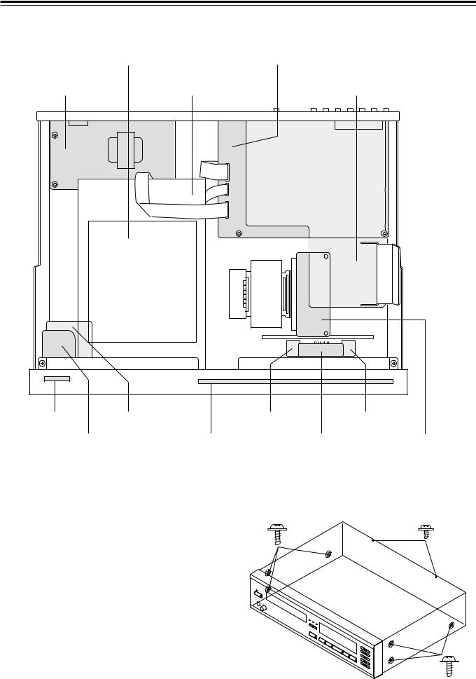
2. REMOVAL PROCEDURES
• Location of Major Parts
DVD Main P.C.B. Ass'y
(Bottom side of Mechanism BLK) |
Digital P.C.B. Ass'y |
|
P-Supply P.C.B. Ass'y |
Mechanism BLK Ass'y |
Output P.C.B. Ass'y |
|
|
|
|
|
|
|
|
|
|
|
|
|
|
|
|
|
|
|
|
|
|
|
|
|
|
|
|
|
|
|
REG 5V P.C.B. Ass'y |
|
|
|
|
|
|
|
|
|
|
||
LED P.C.B. Ass'y H.P P.C.B. Ass'y |
|
REG 3V P.C.B. Ass'y |
|
|
|
|||||
Power-SW P.C.B. Ass'y |
Front P.C.B. Ass'y |
Diode P.C.B. Ass'y |
M-Trance P.C.B. Ass'y |
|||||||
(The Mechanism P.C.B. Ass’y is constructed on the DVD Mechanism Block.)
Fig. 2-1 Top View
2.1 Top Cover (Refer to Fig. 2-2)
1)Remove the 8 screws and detach the Top Cover from the main body.
Fig. 2-2
4
REMOVAL PROCEDURES
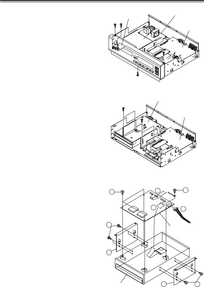
2.2 Front Panel (Refer to Fig. 2-3)
1)Remove the 5 screws on the front panel.
2)Remove the screws holding the H.P P.C.B. Ass’y. The screws can be reached by going through the hole in the left side Power-SW P.C.B. Ass’y.
3)Disconnect the P702 on the P-Supply P.C.B. Ass’y and disconnect the P530 and P200 on the Digital P.C.B. Ass’y.
4)Remove the front panel in front of you by pulling it outward, keeping it level as you pull.
P-Supply P.C.B. Ass'y
H.P P.C.B. Ass'y
Digital
P.C.B. Ass'y
P702
P530
P200
Fig.2-3
2.3 Mechanism Block (Refer to Fig. 2-4)
1)Disconnect the flexible cable from the P550 and P570 on the Digital P.C.B. Ass’y.
2)Disconnect the P540 on the Output P.C.B. Ass’y.
3)Remove the 4 screws and detach the machanism from the
main body.
2.4 DVD Main P.C.B. Ass’y (Refer to Fig. 2-5) |
1 |
1)Remove the 4 screws “1” on the DVD Main P.C.B. Ass’y.
2)Disconnect the three connectors “a” , “b” and “c” on the DVD Main P.C.B. Ass’y.
2
2.5 Mechanism Ass’y (Refer to Fig. 2-5)
1) Remove the DVD Main P.C.B. Ass’y.
2) Remove the 8 screws "2" in the diagram, and then remove the left and right plates "3".
3
Mechanism Block
Digital P.C.B. Ass'y
 P570
P570
 P550
P550
 P540
P540
Fig.2-4 |
|
a |
1 |
c |
b |
|
DVD Main P.C.B. Ass'
Mechanism Ass'y 3 2
Fig.2-5
5
REMOVAL PROCEDURES
2.6. Bottom Cover EX Ass'y, Top Cover EX Ass'y |
6) Pull the edges of the connector CN200 "8" on the Mecha- |
|
|
and F Panel EX Ass'y(Refer to Fig. 2-7) |
nism P.C.B. Ass'y to unlock the connector edges and care- |
1) Remove the 6 screws "1" (M2.6x5 + Pan (#0 Type 3)) and |
fully pull out the Pickup Flexible P.C.B. "9". |
|
|
detach the Bottom Cover EX Ass'y. |
7) Carefully disconnect the 3 connectors CPI04 "10" (EX Mo- |
2) Remove the 2 screws "2" (M2.6x3 + Pan), and detach the |
tor Ass'y), CN50011" " (Sled Motor Ass'y), and CN60012" " |
|
|
Top Cover EX Ass'y and F Panel EX Ass'y. |
(Inner Switch) |
|
|
8) Remove the Mechanism P.C.B. Ass'y from the Mechanism |
2.7. Mechanism P.C.B. Ass'y(Refer to Fig. 2-7) |
Ass'y. |
|
1) Remove the Bottom Cover EX Ass'y, Top Cover EX Ass'y |
|
|
|
and F Panel EX Ass'y. See item 2.6. |
2.8. Loading EX Ass'y(Refer to Fig. 2-7) |
2) |
Shorting the laser diode shorting land of the DVD Traverse |
1) Remove the Mechanism P.C.B Ass'y. See item 2.7. |
|
Ass'y: |
2) Remove the 6 screws "13" (ST2.6x3 + Pan (#0 Type 3)), 1 |
|
Short the laser diode shorting lands (2 places shown by the |
screw "14" (M1.7x2.5 + Pan (#0 Type 3) (Black)), and 4 |
|
arrows) with a soldering iron before removing the Mecha- |
screws "15" (M2x2 + Pan (#0 Type 3) (Black)). |
|
nism P.C.B. Ass'y. |
• Note when reassembling: |
|
Note: Use a soldering iron whose metal part is grounded or |
When reassembling the Mecha Flexible P.C B. Ass'y 5"", |
|
a ceramic soldering iron. |
move it to the front side. |
|
CAUTION: Do not disconnect the Flexible Cable from the |
Be sure that the shutter is positioned in the center of the |
|
connector P200 on the Mechanism P.C.B. Ass'y unless the |
shutter sensor on the Mecha Flexible P.C.B. Ass'y, when the |
|
laser shorting lands (2 places) are shorted. |
shutter of the Loading EX Ass'y is closed by hand, |
|
|
3) Remove the EX Loading Chassis block "16" backward while |
|
|
lifting its to the right side a little. |
|
|
4) Remove the Loading EX Ass'y while lifting it. |
|
|
• Note: Do not damage the Catch Arm Ass'y and the Loading |
|
|
Link Ass'y of the Loading EX Ass'y. |
|
|
2.9. DVD Traverse Ass'y(Refer to Fig. 2-7) |
|
|
1) Remove the Loading EX Ass'y. See item 2.8. |
|
|
2) Remove the 3 screws "17" (ST2 6x3 + Pan (#0 Type 3)) and |
|
|
remove the EX Motor Ass'y. |
|
|
3) Remove the 3 screws "18" (ST2.6x3 + Pan (#0 Type 3)) and |
|
|
remove the EX Chassis Ass'y. |
|
|
4) Remove the 4 pcs. of Damper Screw SL"19", 4 pcs of and |
|
|
SUS Collar B "20", and 4 pcs of SUS Collar T "21", and |
|
|
detach the DVD Traverse Ass'y. |
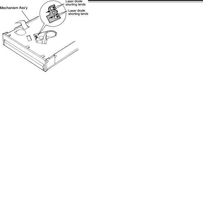
[Shorting the Laser Diode Shorting Lands of the DVD Traverse |
Notes: |
|
Ass'y] |
1. Pay attention so as not to damage the Door Sensor P.C B. |
|
|
|
of the Mecha Flexible P.C.B. "5". |
• |
Note when reassembling: |
2. Assemble the Door Sensor P.C.B. so as not it is inclined. |
|
Unsolder the laser diode shorting lands after reassembling |
3. Be sure that the projection of the Front Door Ass'y can be |
|
the Mechanism P.C.B. Ass'y. |
correctly inserted into the Door Sensor. |
3) Remove 1 screw "3" (M2.6x3.5 + Pan (#0 Type 3)) and 1 |
|
|
|
screw "4" (M2.6x8 + Pan). |
|
4) Disconnect the Mecha Flexible P.C B. Ass'y 5"" by pulling |
|
|
|
the edges of the connector CP103 "6" on the Mechanism |
|
|
P.C.B. Ass'y to unlock the connector edges. |
|
5) |
Pull the edges of the connector CN300 "7" on the Mecha- |
|
|
nism P.C.B. Ass'y to unlock the connector edges and care- |
|
|
fully pull out the Traverse Flexible P.C.B. Ass'y. |
|
6
REMOVAL PROCEDURES
2.6. Top Cover EX Ass'y
2.8. Loading EX Ass'y
2.9.DVD Traverse Ass'y
2.7. Mechanism
P.C.B. Ass'y
2.6. Panel EX Ass'y
2.6. Bottom Cover EX Ass'y
Fig.2-7
7
REMOVAL PROCEDURES
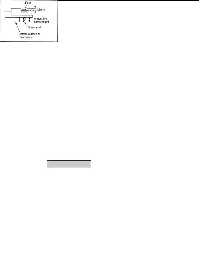
2.10 Pickup (Refer to Fig.2-8)
Caution: Do not remove or loosen screws that are not in-
cluded in this procedure.
Note: After reassembling the Pickup, you need to perform “Tilt Adjustment” of the Pickup.
Preparation:
Since you need to reposition the screw F03 to the original position, check the current position before removing the screw F03.
•Give a mark on the head of screw F03 to allow easy repositioning.
•Check the end position of the screw F03. It will be almost the same as the bottom surface of the chassis.
1)Remove the DVD Traverse Ass’y. Refer to item 2.9.
2)Remove a screw F01 (M1.7x3.5+Pan CMT) and detach F02 (Hook L.S)
3)Give a mark to the screw F03 for repositioning.
4)Remove a screw F03 (Screw S) and detach F04/F05 (Pickup block).
F06 (SP Push Shaft) can be removed.
5)Pull out F04 (Shaft L) from F05 (Pickup).
Notes on reassembling:
•Assemble the screw F03 so that it is roughly positioned to the original position.
•Perform “Tilt Adjustment”. Refer to Stap 3 “Tilt Adjustment” in 3.3 “Adjustment procedure”
Do not remove or loosen
Fig.2-8
8
3. ELECTRICAL ADJUSTMENT
3.1 Measurement instruments and Jigs
1)DC Voltmeter
2)AC Voltmeter
3)Tracking Offset Meter LE-9055A or LTM-9055 (Leader Electronics Corp.)
4)A-BEX Vertical Deviation Test Disc TDV-562 (DA09206A)
5)SONY Test Disc Type 3
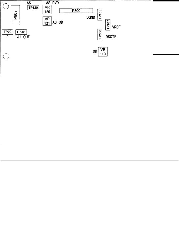
3.2Parts Location for Adjustment
Fig.3-1 Parts Location for Electorical Adjustment (DVD Main P.C.B. Ass’y)
Fig.3-2 Tilt Adjustment Screws (Mechanism Ass’y)
9
ELECTRICAL ADJUSTMENT
3.3 Adjustment procedure (Follow the next steps in order)
STEP |
|
ITEM |
SIGNAL |
|
OUTPUT |
ADJUSTMENT |
|
|
REMARKS |
|
||||||||||||||||
|
SOURCE |
|
CONNECTION |
|
|
|
||||||||||||||||||||
|
|
|
|
|
|
|
|
|
|
|
|
|
|
|
|
|
|
|
|
|
|
|||||
1 |
DVD Adjust |
|
|
|
|
|
|
|
|
1. |
Connect each measuring instrument as follows: |
|||||||||||||||
|
|
Mode |
|
|
|
|
|
|
|
|
|
• Connect a DC voltmeter between TP120 (AS) (+ terminal) |
||||||||||||||
|
|
|
|
|
|
|
|
|
|
|
|
|
|
|
|
|
|
and TP107 (VREF) (- terminal) on the DVD Main P.C.B. Ass’y. |
||||||||
|
|
|
|
|
|
|
|
|
|
|
|
|
|
|
|
|
|
• Connect an AC voltmeter between TP201 (JI OUT) (+ termi- |
||||||||
|
|
|
|
|
|
|
|
|
|
|
|
|
|
|
|
|
|
nal) and TP105 (DGND) (-terminal) on the DVD Main P.C.B. |
||||||||
|
|
|
|
|
|
|
|
|
|
|
|
|
|
|
|
|
|
|||||||||
|
|
|
|
|
|
|
|
|
|
|
|
|
|
|
|
|
|
Ass’y. |
|
|
|
|
|
|
|
|
|
|
|
|
|
|
|
|
|
|
|
|
|
|
|
Disc |
3 button |
|
• Connect a tracking offset meter between TP300 (DSCTE) (+ |
||||||||
|
|
|
|
|
|
|
|
|
|
|
|
|
|
|
|
|||||||||||
|
|
|
|
|
|
|
|
|
|
|
|
|
|
|
|
|||||||||||
|
|
|
|
|
|
|
|
|
|
|
|
|
|
|
|
|||||||||||
|
|
|
|
|
|
|
|
|
|
|
|
|
|
|
|
terminal) and TP107 (VREF) (-terminal) on the DVD Main |
||||||||||
|
|
|
|
|
|
|
|
|
|
|
|
|
|
|
|
|||||||||||
|
|
|
|
|
|
|
|
|
|
|
|
|
|
|
|
|
|
|||||||||
|
|
|
|
|
|
|
|
|
|
|
|
|
|
|
|
|
|
P.C.B. Ass’y. |
|
|
|
|
|
|
|
|
|
|
|
|
|
|
|
|
|
|
|
|
|
|
|
|
|
|
|
|
|
|
|
|
|
|
|
|
|
|
|
|
|
|
|
|
|
|
|
|
|
|
|
|
|
|
|
|
|
|
|
|
|
|
|
|
|
|
|
|
|
|
|
|
|
|
|
|
|
|
|
2. While pressing and holding the STOP button, press the POWER |
|||||||||
|
|
|
|
|
|
|
|
|
|
|
|
|
|
|
|
|
|
button, then enter standby mode. (the indicator will light orange). |
||||||||
|
|
|
|
|
|
|
|
|
|
|
|
|
|
|
|
|
|
|||||||||
|
Eject button Forward Skip Play button |
|
Stop button |
|
|
3. Press the PAUSE ( |
) button and DISC 3 button for more than 2 |
|||||||||||||||||||
|
|
|
|
|
|
|
||||||||||||||||||||
|
|
|
|
|
|
|
button |
Pause button |
|
|
|
seconds to engage the test mode. |
|
|||||||||||||
|
|
|
|
|
|
|
|
|
|
|
|
|
|
|||||||||||||
|
|
|
|
|
|
|
|
|
|
|
|
|
|
|
|
|
|
|
||||||||
|
|
|
|
|
|
|
|
|
|
|
|
|
|
|
|
|
|
Confirm that the following message appears on the display. |
||||||||
|
|
|
|
|
|
|
|
|
|
|
|
|
|
|
|
|
|
DVD ADJUST → |
DISC 1 T - 01 |
|
||||||
|
|
|
|
|
|
|
|
|
|
|
|
|
|
|
|
|
|
|
||||||||
|
|
|
|
|
|
|
|
|
|
|
|
|
|
|
|
|
|
|
||||||||
2 |
|
AS |
|
|
DC Voltmeter |
VR120 |
|
Note: Perform the adjustment in the order of “CD LD ON” and |
||||||||||||||||||
|
|
Adjustment |
|
|
between |
(for DVD,LD) |
|
“DVD LD ON” as mentioned below: |
|
|||||||||||||||||
|
|
|
|
|
|
|
|
|
|
|
TP120(AS)(+) |
|
|
1. |
Press the STOP ( |
) button once. |
|
|||||||||
|
|
|
|
|
|
|
|
|
|
|
|
|
|
The message will change as follows: |
||||||||||||
|
|
|
|
|
|
|
|
|
|
|
and |
VR121 |
|
|||||||||||||
|
|
|
|
|
|
|
|
|
|
|
|
→ AS ADJUST → |
DVD LD ON |
|
||||||||||||
|
|
|
|
|
|
|
|
|
|
TP107(VREF)(-) |
(for CD,LD) |
|
|
|||||||||||||
|
|
|
|
|
|
|
|
|
|
2. Adjust VR120 to obtain 0V ± 10 mV DC on the DC voltmeter. |
||||||||||||||||
|
|
|
|
|
|
|
|
|
|
|
on DVD Main |
|
|
|||||||||||||
|
|
|
|
|
|
|
|
|
|
|
|
|
3. |
Press the FORWARD SKIP ( |
|
|
|
|
) button once. |
|||||||
|
|
|
|
|
|
|
|
|
|
|
P.C.B. Ass’y |
|
|
|
|
|
|
|||||||||
|
|
|
|
|
|
|
|
|
|
|
|
|
|
The following message will appear on the display, |
||||||||||||
|
|
|
|
|
|
|
|
|
|
|
|
|
|
|
|
|
|
→ CD LD ON |
|
|
|
|
|
|
|
|
|
|
|
|
|
|
|
|
|
|
|
|
|
|
|
|
|
4. |
Adjust VR121 to obtain 0V ± 10 mV DC on the DC voltmeter. |
||||||||
|
|
|
|
|
|
|
|
|
|
|
|
|
|
|
|
|
5. |
Press the FORWARD SKIP ( |
|
|
|
|
) button again to select “DVD |
|||
|
|
|
|
|
|
|
|
|
|
|
|
|
|
|
|
|
|
|||||||||
|
|
|
|
|
|
|
|
|
|
|
|
|
|
|
|
|
|
|||||||||
|
|
|
|
|
|
|
|
|
|
|
|
|
|
|
|
|
|
LD ON”, and confirm that the DC voltage is at the level that it was |
||||||||
|
|
|
|
|
|
|
|
|
|
|
|
|
|
|
|
|
|
adjusted to in step 2. If there is any deviance to the DC voltage, |
||||||||
|
|
|
|
|
|
|
|
|
|
|
|
|
|
|
|
|
|
re-adjust. |
|
|
|
|
|
|
|
|
|
|
|
|
|
|
|
|
|
|
|
|
|
|
|
|
|
6. |
Press the FORWARD SKIP ( |
|
|
|
|
) button twice. |
|||
|
|
|
|
|
|
|
|
|
|
|
|
|
|
|
|
|
|
|||||||||
|
|
|
|
|
|
|
|
|
|
|
|
|
|
|
|
|
|
|||||||||
|
|
|
|
|
|
|
|
|
|
|
|
|
|
|
|
|
|
The following message will appear on the display. |
||||||||
|
|
|
|
|
|
|
|
|
|
|
|
|
|
|
|
|
|
CD LD ON → LD OFF |
|
|||||||
|
|
|
|
|
|
|
|
|
|
|
|
|
|
|
|
|
|
The pickup will then move to the innermost position and stops |
||||||||
|
|
|
|
|
|
|
|
|
|
|
|
|
|
|
|
|
|
there. |
|
|
|
|
|
|
|
|
|
|
|
|
|
|
|
|
|
|
|
|
|
|
|
|
|
7. Proceed to the next step. |
|
||||||||
|
|
|
|
|
|
|
|
|
|
|
|
|
|
|
|
|
|
|
|
|
||||||
3 |
|
Tilt |
DVD Vertical |
|
AC Voltmeter |
Tilt Screws |
1. |
Press the STOP ( |
) button once. |
|
||||||||||||||||
|
|
Adjustment |
Deviation |
|
between |
A and B |
|
Be sure that the following message appears on the display. |
||||||||||||||||||
|
|
|
|
→ MECHA ADJUST |
|
|||||||||||||||||||||
|
|
|
|
|
|
|
|
|
|
|
TP201(JI OUT) |
|
|
|
|
|||||||||||
|
|
|
|
|
|
|
|
|
|
|
|
|
2. |
Press the EJECT ( |
) button and insert the DVD Test Disc. |
|||||||||||
|
|
|
|
|
|
|
|
|
Test Disc |
|
(+) and |
|
|
|||||||||||||
|
|
|
|
|
|
|
|
|
|
|
|
3. |
Press the PLAY ( |
) button to play back the disc. |
||||||||||||
|
|
|
|
|
|
|
|
|
TDV-562 |
TP105(DGND)(-) |
|
|
||||||||||||||
|
|
|
|
|
|
|
|
|
|
|
4. |
Press the FORWARD SKIP ( |
|
|
) button to play back the |
|||||||||||
|
|
|
|
|
|
|
|
|
|
|
|
|||||||||||||||
|
|
|
|
|
|
|
|
|
|
on DVD Main |
|
|
|
|||||||||||||
|
|
|
|
|
|
|
|
|
(DA09206) |
|
|
|
|
Chapter 16 (outermost track). |
|
|||||||||||
|
|
|
|
|
|
|
|
|
|
|
P.C.B. Ass’y |
|
|
5. |
Press the PAUSE ( |
) button to pause the disc. (The disc will |
||||||||||
|
|
|
|
|
|
|
|
|
|
|
|
|
|
|
|
|
|
keep turning.) |
|
|
|
|
|
|
|
|
|
|
|
|
|
|
|
|
|
|
|
|
|
|
|
|
|
6. Turn Screw A to obtain the minimum reading on the AC voltmeter. |
|||||||||
|
|
|
|
|
|
|
|
|
|
|
|
|
|
|
|
|
7. Turn Screw B to obtain the minimum reading on the AC voltmeter. |
|||||||||
|
|
|
|
|
|
|
|
|
|
|
|
|
|
|
|
|
8. Repeat steps 6 and 7 several times until the minimum readings |
|||||||||
|
|
|
|
|
|
|
|
|
|
|
|
|
|
|
|
|
|
are obtained. |
|
|
|
|
|
|
|
|
|
|
|
|
|
|
|
|
|
|
|
|
|
|
|
|
|
9. |
Press the EJECT ( |
) button to eject the disc. |
|||||||
|
|
|
|
|
|
|
|
|
|
|
|
|
|
|
|
|
10.Proceed to the next step. |
|
||||||||
|
|
|
|
|
|
|
|
|
|
|
|
|
|
|
|
|
|
|
|
|
|
|
|
|
|
|
10
ELECTRICAL ADJUSTMENT
STEP |
ITEM |
SIGNAL |
OUTPUT |
ADJUSTMENT |
REMARKS |
|
SOURCE |
CONNECTION |
|||||
|
|
|
|
4 CD Tracking CD Test Disc |
Tracking Offset |
VR110 |
1. |
Set the tracking offset meter as follows: |
|||
Adjustment |
SONY |
Meter |
|
|
• |
Sensitivity switch: |
HIGH (right side) |
|
Type 3 |
between |
|
|
• |
Level switch: |
MEASURE (left side) |
|
|
TP300(DSCTE) (+) |
|
|
• |
Center switch: |
MEASURE (center position) |
|
|
|
2. |
Insert the CD Test Disc. |
|||
|
|
and |
|
||||
|
|
|
3. |
Press the STOP ( |
) button once. |
||
|
|
TP107(VRFE)(-) |
|
||||
|
|
|
|
Be sure that the following message appears on the display. |
|||
|
|
on Main P.C.B. |
|
|
|||
|
|
|
|
|
→ CD ADJUST |
|
|
|
|
|
|
|
|
|
|
|
|
|
|
4. |
Adjust VR110 so that the center meter indicates 0 V as shown on |
||
|
|
|
|
|
the left. Also, be sure that the left side meter indicates around 1 V. |
||
|
|
|
|
5. |
Press the EJECT ( |
) button to eject the disc. |
|
|
|
|
|
6. |
Proceed to the next step to terminate the adjustment. |
||
When adjustment is finished, detach the voltmeter and press the Power button to turn the power off. The TEST MODE will be released once the power is off.
Apply paint lock the Screw A and B.
3.4 RAM Clear (System Controller & Mechanism Controller Clear)
Note: Before shipping perform the RAM Clear to perform the followings:
•To clear the usable setting values to the initial setting values.
•To perform initialization operation of the changer mechanism.
STEP |
ITEM |
SIGNAL |
OUTPUT |
ADJUSTMENT |
|
REMARKS |
|
SOURCE |
CONNECTION |
|
|||||
|
|
|
|
|
|
||
|
|
|
|
|
|
|
|
1 |
RAM Clear |
|
|
|
1. While pressing and holding |
the STOP button, press the POWER |
|
|
|
|
|
|
button, then enter standby mode. |
||
|
|
|
|
|
2. Remove all discs. |
|
|
|
|
|
|
|
3. Press and hold the PAUSE ( |
) and DISC 4 buttons for more than |
|
|
|
|
|
|
7 seconds. |
|
|
|
|
|
|
|
4. The following messages will appear on the display. |
||
|
|
|
|
|
RAM CLEAR 2 |
|
|
|
|
|
|
|
↓ |
(After 5 seconds) |
|
|
|
|
|
|
REGION X (X: 0 to 8) |
|
|
|
|
|
|
|
5. Then, the following operation will be done. |
||
|
|
|
|
|
• User setting values are reset to the initial setting values. |
||
|
|
|
|
|
• Changer mechanism is initialized. |
||
|
|
|
|
|
6. “Power OFF” will be displayed and the system is automatically shut |
||
|
|
|
|
|
off. |
|
|
|
|
|
|
|
POWER OFF (Standby mode) |
||
|
|
|
|
|
If the disc remains in the changer mechanism, power is not shut off |
||
|
|
|
|
|
and the display returns to the normal one. |
||
|
|
|
|
|
|
|
|
11
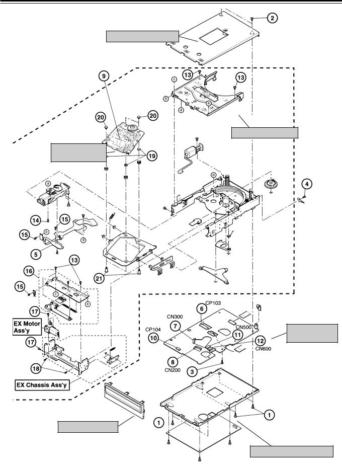
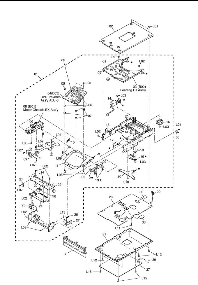
4. MECHANICAL ASS’Y AND PARTS LIST
4.1 Synthesis Ass’y
<![if ! IE]><![endif]>L04
<![if ! IE]><![endif]>L04
| <![if ! IE]> <![endif]>L04 |
|
| <![if ! IE]> <![endif]>L05 |
|
|
<![if ! IE]> <![endif]>L02 |
|
<![if ! IE]> <![endif]>A |
|
<![if ! IE]> <![endif]>D |
| <![if ! IE]> <![endif]>L04 |
<![if ! IE]> <![endif]>D |
|
|
| <![if ! IE]> <![endif]>23 |
<![if ! IE]> <![endif]>19 |
| <![if ! IE]> <![endif]>A |
|
|
<![if ! IE]> <![endif]>L02 |
<![endif]>L02
|
|
|
|
|
|
<![if ! IE]> <![endif]>D’ |
|
|
|
<![if ! IE]> <![endif]>25 |
|
|
|
|
|
|
<![if ! IE]> <![endif]>26 |
| <![if ! IE]> <![endif]>24 |
|
|
|
|
|
<![if ! IE]> <![endif]>C’ |
|
|
|
|
|
|
|
|
<![if ! IE]> <![endif]>D’ |
|
|
|
|
<![if ! IE]> <![endif]>B’ |
|
|
|
|
|
|
|
|
|
|
|
|
<![if ! IE]> <![endif]>B’ |
|
|
| <![if ! IE]> <![endif]>L10 |
|
<![if ! IE]> <![endif]>L11 |
<![if ! IE]> <![endif]>C’ |
|
<![if ! IE]> <![endif]>C’ |
|
<![if ! IE]> <![endif]>J |
|
|
|
|
<![if ! IE]> <![endif]>B’ |
|
|
|
|
<![if ! IE]> <![endif]>C’ |
| <![if ! IE]> <![endif]>D |
|
|
|
|
<![if ! IE]> <![endif]>A’ |
|
|
|
|
|
|
|
|
<![if ! IE]> <![endif]>D’ |
|
|
|
| <![if ! IE]> <![endif]>D |
|
|
|
|
|
|
<![if ! IE]> <![endif]>H’ |
|
| <![if ! IE]> <![endif]>20 |
|
<![if ! IE]> <![endif]>C |
|
|
|
<![if ! IE]> <![endif]>E’ |
|
|
|
|
<![if ! IE]> <![endif]>21 |
<![if ! IE]> <![endif]>D’ |
|
|
|
|
|
|
|
<![if ! IE]> <![endif]>J’ |
|
|
|
|
|
|
| <![if ! IE]> <![endif]>L09 |
<![if ! IE]> <![endif]>B |
<![if ! IE]> <![endif]>J’ |
<![if ! IE]> <![endif]>A’ |
|
|
<![if ! IE]> <![endif]>E’ |
|
<![if ! IE]> <![endif]>F’ |
|
|
|
<![if ! IE]> <![endif]>A’ |
|
<![if ! IE]> <![endif]>E’ |
|
|
|
|
|
|
<![if ! IE]> <![endif]>C |
|
|
|
|
|
| <![if ! IE]> <![endif]>22 |
|
<![if ! IE]> <![endif]>C |
|
|
<![if ! IE]> <![endif]>E’ |
|
<![if ! IE]> <![endif]>28 |
<![if ! IE]> <![endif]>L12 |
| <![if ! IE]> <![endif]>B |
|
<![if ! IE]> <![endif]>C |
|
|
|
|
|
|
| <![if ! IE]> <![endif]>L09 |
|
<![if ! IE]> <![endif]>L09 |
<![if ! IE]> <![endif]>L08 |
<![if ! IE]> <![endif]>H’ |
<![if ! IE]> <![endif]>G’ |
|
<![if ! IE]> <![endif]>26 |
<![if ! IE]> <![endif]>27 |
|
|
|
<![if ! IE]> <![endif]>E |
|
|
|
|
|
|
|
|
|
<![if ! IE]> <![endif]>E |
<![if ! IE]> <![endif]>L06 |
|
|
|
|
|
|
|
<![if ! IE]> <![endif]>L06 |
|
|
|
|
| <![if ! IE]> <![endif]>A01 |
|
|
<![if ! IE]> <![endif]>L07 |
|
|
|
<![if ! IE]> <![endif]>16 |
|
|
|
|
|
|
|
<![if ! IE]> <![endif]>17 |
|
<![if ! IE]> <![endif]>15 |
|
|
<![if ! IE]> <![endif]>E |
|
|
|
|
|
|
|
|
|
|
|
|
<![if ! IE]> <![endif]>13 |
|
|
|
|
<![if ! IE]> <![endif]>L06 |
|
|
<![if ! IE]> <![endif]>L04 |
<![if ! IE]> <![endif]>H |
|
<![if ! IE]> <![endif]>8 |
| <![if ! IE]> <![endif]>L08 |
|
<![if ! IE]> <![endif]>E |
|
<![if ! IE]> <![endif]>18 |
|
|
|
|
|
|
|
|
|
|
|
|
|
|
|
<![if ! IE]> <![endif]>L07 |
|
<![if ! IE]> <![endif]>14 |
|
|
|
|
| <![if ! IE]> <![endif]>27 |
<![if ! IE]> <![endif]>L04 |
<![endif]>L04
<![if ! IE]><![endif]>L13
<![if ! IE]><![endif]>30
<![if ! IE]><![endif]>L12
| <![if ! IE]> <![endif]>29 |
<![if ! IE]> <![endif]>L12 |
<![endif]>L04
| <![if ! IE]> <![endif]>L01 |
<![if ! IE]> <![endif]>L06 |
|
<![if ! IE]> <![endif]>12 |
|
<![if ! IE]> <![endif]>L03 |
|
<![if ! IE]> <![endif]>10 |
|
<![if ! IE]> <![endif]>L04 |
|
<![if ! IE]> <![endif]>L04 |
<![endif]>9
| <![if ! IE]> <![endif]>11 |
<![if ! IE]> <![endif]>7 |
<![endif]> G
G
<![endif]> H
H
<![endif]>6
<![if ! IE]><![endif]>F
<![if ! IE]><![endif]>L03
| <![if ! IE]> <![endif]>1 |
<![if ! IE]> <![endif]>6 |
| <![if ! IE]> <![endif]>L01 |
|
|
<![if ! IE]> <![endif]>2 |
|
<![if ! IE]> <![endif]>5 |
| <![if ! IE]> <![endif]>3 |
<![if ! IE]> <![endif]>4 |
Fig.4-1
12

MECHANICAL ASS’Y AND PARTS LIST
4.1 Synthesis Ass’y
Ref. No. |
Part No. |
Description |
Q'ty |
|
Ref. No. |
Part No. |
Description |
Q'ty |
1 |
0H08831A |
Top Cover BK |
1 |
|
|
BK10564A |
DIGITAL P.C.B. Ass’y Other NTSC |
1 |
|
|
(USA/CAN/UK/EP/AUS/DA) |
|
|
|
|
(KR/DA/TW) |
|
|
0H08832A |
Top Cover CG |
1 |
|
|
BK10566A |
DIGITAL P.C.B. Ass’y Other PAL |
1 |
|
|
(CH/JPN/OTR/HK/KR/TW) |
|
|
|
|
(CH/HK/AUS/OTR) |
|
2 |
0H08583C |
Dress Panel BK |
1 |
21 |
BK10255A |
OUTPUT P.C.B. Ass’y |
1 |
|
|
|
(USA/CAN/UK/EP/AUS/DA) |
|
|
|
|
(Except JPN/EP/UK) |
|
|
0H08584C |
Dress Panel CG |
1 |
|
|
BK10377A |
OUTPUT P.C.B. Ass’y |
1 |
|
|
(CH/JPN/OTR/HK/KR/TW) |
|
|
|
|
(JPN) |
|
3 |
2H00138A |
Logo Plate BK |
1 |
|
|
BK10378A |
OUTPUT P.C.B. Ass’y |
1 |
|
|
(USA/CAN/UK/EP/AUS/DA) |
|
|
|
|
(EP/UK) |
|
|
2H00139A |
Logo Plate CG |
1 |
22 |
0B85640A |
FFC 17P |
1 |
|
|
|
(CH/JPN/OTR/HK/KR/TW) |
|
23 |
0B70300A |
Slide SW L12-22A2 (SW701) |
1 |
|
4 |
0H08600A |
Power Knob BK |
1 |
|
|
|
(OTR/DA/TW only) |
|
|
|
(USA/CAN/UK/EP/AUS/DA) |
|
24 |
0B50459A |
Power Transformer 100-120V |
1 |
|
|
0H09025A |
Power Knob CG |
1 |
|
|
|
(JPN/USA/CAN) |
|
|
|
(CH/JPN/OTR/HK/KR/TW) |
|
|
|
0B50460A |
Power Transformer 115-230V |
1 |
5 |
0H07985A |
Headphone Volume knob BK |
1 |
|
|
|
(Except JPN/USA/CAN) |
|
|
|
(USA/CAN/UK/EP/AUS/DA) |
|
25 |
BK10376A |
M-Trans P.C.B. Ass’y |
1 |
|
|
0H09026A |
Headphone Volume knob CG |
1 |
26 |
0H08470A |
55 Foot A |
4 |
|
|
|
(CH/JPN/OTR/HK/KR/TW) |
|
27 |
0J08423A |
Foot Sheet (20) |
4 |
|
6 |
0H08500A |
Indicator |
4 |
28 |
BK10565A |
DIODE P.C.B. Ass’y |
1 |
|
7 |
0H08596C |
Display Lens |
1 |
29 |
BK10557A |
REG.3V P.C.B. Ass’y |
1 |
|
8 |
0H08585E |
Front Panel BK |
1 |
30 |
BK10556A |
REG.5V P.C.B. Ass’y |
1 |
|
|
|
(USA/CAN/UK/EP/AUS/DA) |
|
|
A01 |
----------- |
MECHANISM Ass’y DVD-15 |
1 |
|
0H08586D |
Dress Panel CG |
1 |
|
L01 |
0E03032A |
BT4x8+Washer Faced (Black) |
|
|
|
(CH/JPN/OTR/HK/KR/TW) |
|
|
|
|
(USA/CAN/UK/EP/AUS/DA) |
|
9 |
BK10268A |
POW SW P.C.B. Ass’y |
1 |
|
|
0E04146A |
BT4x8+Pan Flange |
|
10 |
BK10257A |
LED P.C.B. Ass’y |
1 |
|
|
|
(CH/JPN/OTR/HK/KR/TW) |
|
11 |
BK10254A |
HP P.C.B. Ass’y Except EP |
1 |
|
L02 |
0E03632A |
BT3x8+Binding with washer (Black) |
|
|
BK10574A |
HP P.C.B. Ass’y |
1 |
|
|
|
(USA/CAN/UK/EP/AUS/DA) |
|
|
|
(EP/UK) |
|
|
|
0E04147A |
BT3x8+Binding with washer |
|
12 |
0J08637A |
Line Cord washar |
1 |
|
|
|
(CH/JPN/OTR/HK/KR/TW) |
|
13 |
0H08592B |
Control Button BK |
1 |
|
L03 |
0E03897A |
BT3x10+Binding Projected (Black) |
|
|
|
(USA/CAN/UK/EP/AUS/DA) |
|
|
|
|
(USA/CAN/UK/EP/AUS/DA) |
|
|
0H08593B |
Control Button CG |
1 |
|
|
0E04372A |
BT3x10+Binding Projected |
|
|
|
(CH/JPN/OTR/HK/KR/TW) |
|
|
|
|
(CH/JPN/OTR/HK/KR/TW) |
|
14 |
0H08605B |
Control Lens |
1 |
|
L04 |
0E00921A |
BT3x8+Binding (Black) |
|
15 |
0H08590B |
Disc Select Button BK |
1 |
|
L05 |
0E03137A |
M3x10+Binding (OTR/DA/TW) |
|
|
|
(USA/CAN/UK/EP/AUS/DA) |
|
|
L06 |
0E00865A |
BT3x10+Binding |
|
|
0H08591B |
Disc Select Button CG |
1 |
|
L07 |
0E03854A |
BT3x6+Binding with washer |
|
|
|
(CH/JPN/OTR/HK/KR/TW) |
|
|
L08 |
0E00992A |
M3x4+Binding |
|
16 |
0H08604B |
Disc Select Lens |
5 |
|
L09 |
0E00877A |
ST3x5+Binding |
|
17 |
0B85637A |
FFC 13P |
1 |
|
L10 |
0E03438A |
ST4x6+Binding |
|
18 |
BK10253A |
FRONT P.C.B. Ass’y |
1 |
|
L11 |
0E00857A |
BT3x6+Binding |
|
19 |
BK10269A |
P-SUPPLY P.C.B. Ass’y |
1 |
|
L12 |
0E00986A |
M3x10+Binding |
|
|
|
(USA/CAN) |
|
|
L13 |
0E00896A |
M3x6+Binding |
|
|
BK10379A |
P-SUPPLY P.C.B. Ass’y |
1 |
|
L14 |
0E00964A |
M3x5+Binding |
|
|
|
(JPN) |
|
|
|
|
|
|
|
BK10380A |
P-SUPPLY P.C.B. Ass’y |
1 |
|
|
|
|
|
|
|
(DA/OTR) |
|
|
|
|
|
|
|
BK10381A |
P-SUPPLY P.C.B. Ass’y |
1 |
|
|
|
|
|
|
|
(EP/UK) |
|
|
|
|
|
|
|
BK10382A |
P-SUPPLY P.C.B. Ass’y |
1 |
|
|
|
|
|
|
|
(CH/HK/KR/SA) |
|
|
|
|
|
|
|
BK10383A |
P-SUPPLY PCB Ass’y |
1 |
|
|
|
|
|
|
|
(TW) |
|
|
|
|
|
|
20 |
BK10258A |
DIGITAL P.C.B. Ass’y |
1 |
|
|
|
|
|
|
|
(USA/CAN) |
|
|
|
|
|
|
|
BK10562A |
DIGITAL P.C.B. Ass’y |
1 |
|
|
|
|
|
|
|
(JPN) |
|
|
|
|
|
|
|
BK10563A |
DIGITAL P.C.B. Ass’y |
1 |
|
|
|
|
|
|
|
(EP/UK) |
|
|
|
|
|
|
13
MECHANICAL ASS’Y AND PARTS LIST
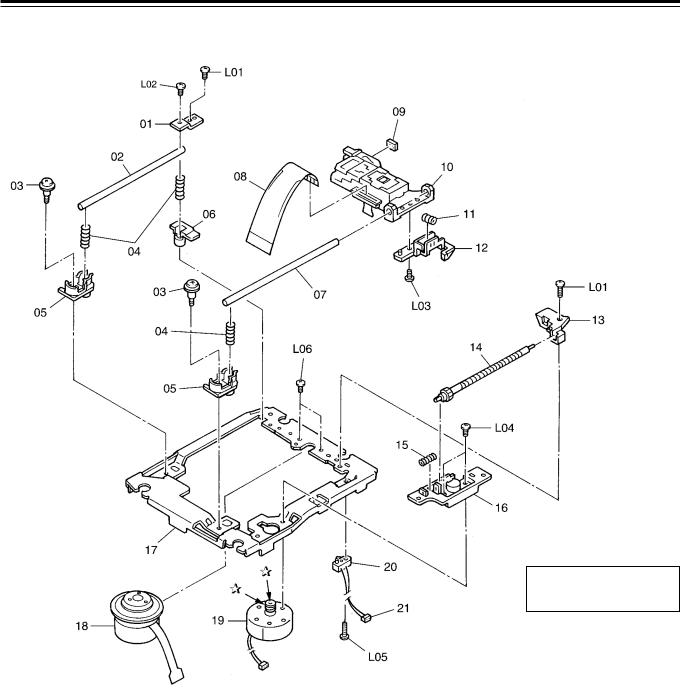
4.2 Mechanism Ass’y DVD-15 (A01)
Fig.4-2
14

MECHANICAL ASS’Y AND PARTS LIST
4.2 Mechanism Ass’y DVD-15 (A01)
Ref. No. |
Part No. |
Description |
Q'ty |
A01 |
--------- |
Mechanism Ass’y Black |
|
|
--------- |
Mechanism Ass’y Gold |
|
01 |
CG09508A |
Machanism Deck Ass’y ADJ-3 |
1 |
02 |
CA09393A |
Top Cover EX Ass’y |
1 |
03 |
CA09505A |
Loading EX Ass’y |
1 |
04 |
CA09479A |
DVD Traverse Ass’y ADJ-3 |
1 |
05 |
0C10325B |
SUS Collar T |
4 |
06 |
0C10326A |
SUS Collar B |
4 |
07 |
0C10279A |
Damper S SL |
4 |
08 |
CA09415A |
Motor Chassis EX Ass’y |
1 |
09 |
BA09736A |
Mecha Flexible P.C.B. Ass’y |
1 |
10 |
0C10286A |
Anti Rattle Spring SL |
1 |
11 |
CA09392B |
SUS Base ADT S Ass’y |
1 |
12 |
0C10185B |
Mechanism UD Sub Cam SL |
1 |
13 |
0C10186A |
UD S Cam Guide SL |
2 |
14 |
CA09351A |
Stocker Motor SL Ass’y |
1 |
15 |
0J08004A |
Dust Seal Emergency SL |
1 |
16 |
0C10175A |
Stocker Position Gear SL |
1 |
17 |
0C10211B |
Plate Spring SL |
1 |
18 |
0C10184A |
Disc Lock Spring SL |
1 |
19 |
0C10183A |
Disc Lock Arm SL |
1 |
20 |
0C10187A |
UD Link Arm SL |
1 |
22 |
0C10306C |
EX Loading Chassis |
1 |
23 |
0C10351A |
EX Loading Return Spring |
1 |
24 |
CA09407A |
Mov G Plat Ass’y |
1 |
25 |
CA09408A |
EX Motor Ass’y |
1 |
26 |
0C10250A |
Shutter Spring SL |
1 |
27 |
0C10305B |
Sub Cam Extension |
1 |
28 |
BA10323A |
Mechanism P.C.B. Ass’y (C3M1) |
1 |
29 |
0J08023A |
Heat sink Reg |
1 |
30 |
HA08369C |
ME F Panel Ass’y BK |
1 |
|
|
(UK/EP/USA/CAN/AUS/DA) |
|
|
HA08370C |
ME F Panel Ass’y CG |
1 |
|
|
(JPN/DU/CH/HK/KR/TW) |
|
31 |
CA09394A |
Bottom Cover EX Ass’y |
1 |
32 |
0B85926A |
FFC 14P |
1 |
33 |
0B85438A |
40P Flexible Wire |
1 |
35 |
0B85437A |
30P Flexible Wire (Pickup) |
1 |
36 |
0B85493A |
1P Wire GND D202 |
1 |
37 |
BK10567A |
DVD Main P.C.B. Ass’y (C3M1) |
1 |
38 |
0C10350A |
D Guide upside Ex |
1 |
39 |
0B85927A |
FFC 24P |
1 |
L01 |
0E00120A |
M2.6x3+Pan |
|
L02 |
0E03964A |
ST2.6x3+Pan (#0 Type 3) |
|
L03 |
0E03955A |
Cut Washer 2.2x4.2x0.2 |
|
L04 |
0E04036A |
M2.6x8+Pan |
|
L05 |
0C10287A |
Damper Screw SL |
|
L06 |
0E03845A |
M1.7x2.5+Pan (#0 Type 3) (Black) |
|
L07 |
0E03945A |
M2x2+Pan (#0 Type 3) (Black) |
|
L08 |
0E03953A |
M2x2+Pan (#0 Type 1) |
|
L09 |
0E03971A |
Pet Washer |
|
L10 |
0E03956A |
Cut Washer 3.2x5.2x0.2 |
|
L11 |
0E03947A |
M2.6x3.5+Pan (#0 Type 3) |
|
L12 |
0E04032A |
M2.6x5+Pan (#0 Type 3) |
|
L13 |
0E03954A |
Cut Washer 1.6x3.2x0.2 |
|
L14 |
0E00955A |
BT2x4+Binding |
|
L15 |
0E00964A |
M3x5+Binding |
|
We suggest that you use grease FL-955/G-4270 or equivalent type.
The company dealing FL-955/G-4270 is as follows:
• FL-955 : Kanto Chemicals Co., Ltd.
2-7 Kanda Sakuma-cho, Chiyoda-ku, Tokyo, Japan
Apply FL-955 (grease) to the following places (marked with ) when parts are replaced.
Ref. No. |
Location |
Remarks |
03 |
Loading EX Ass’y |
|
|
Edges which areinserted into the chassis plate |
|
11 |
SUS Bass ADT S Ass’y |
|
|
• Contact part with the Plate Spring SL (Ref. No. 17) |
|
12 |
Mecha UD Sub Cam SL |
Whole surface |
13 |
UD S Cam Guide SL (2 pcs.) |
Whole surface |
14Stocker Motor SL Ass’y
•Motor Shaft Worm Gear
•Motor Shaft End
17 |
Plate Spring SL |
|
|
Contact part (bottom end) with the SUS Base X Sub |
|
|
Ass’y (Ref, No. 11) |
|
19 |
Disc Lock Arm SL |
Whole surface |
20UD Link Arm SL
• Around the Top End
---Shaft for UD Link Arm SL (Ref. No. 20)
15
MECHANICAL ASS’Y AND PARTS LIST
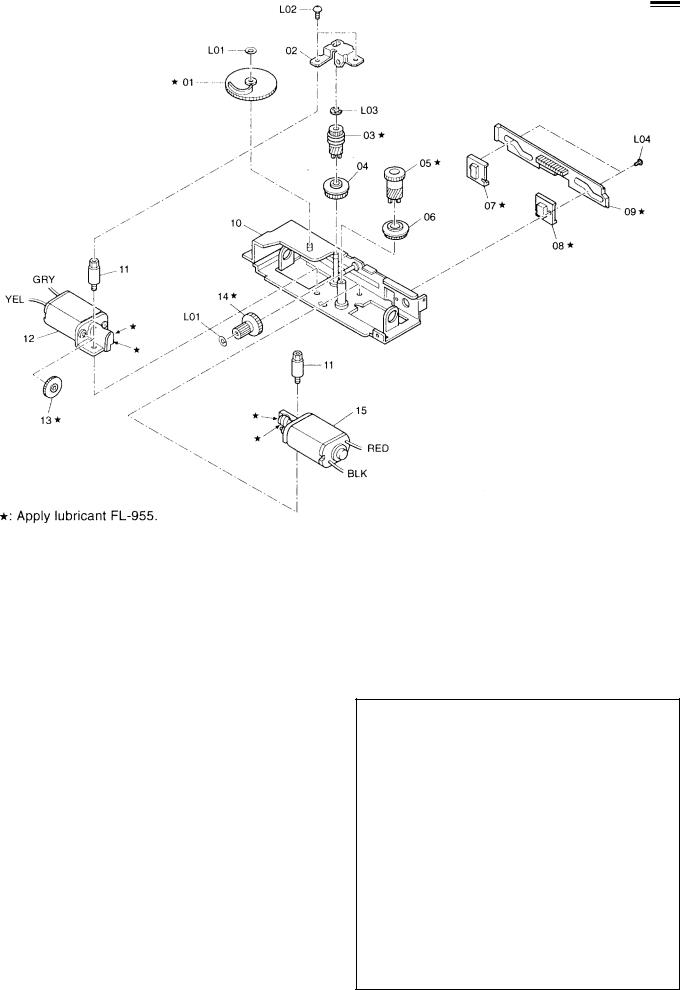
4.3 Motor Chassis EX Ass’y (B01)
Fig.4-3
4.3 Motor Chassis EX Ass’y (B01)
Ref. No. |
Part No. |
Description |
Q'ty |
B01 |
CA09415A |
Motor Chassis EX Ass’y |
|
01 |
0C10238A |
Loading Plate Cam SL |
1 |
02 |
0C10240A |
UD Worm Plate SL |
1 |
03 |
0C10233A |
UD Worm Gear SL |
1 |
04 |
0C10235A |
Mecha Sensor Ring SL |
1 |
05 |
0C10236A |
Loading Worm Gear SL |
1 |
06 |
0C10237A |
Loading Sensor Ring SL |
1 |
07 |
0C10208A |
UD Cam Guide SL |
1 |
08 |
0C10242A |
UD Cam Guide W SL |
1 |
09 |
0C10232A |
UD Cam SL |
1 |
10 |
CA09338A |
Motor Chassis SA S Ass’y |
1 |
11 |
0C10241A |
Bracket Screw SL |
2 |
12 |
CA09417A |
UD Motor EX Ass’y |
1 |
13 |
0C10239A |
Emergency Gear SL |
1 |
14 |
0C10234A |
Mecha UD Gear SL |
1 |
15 |
CA09416A |
Loading Motor EX Ass’y |
1 |
L01 |
0E03955A |
Cut Washer 2.2x4.2x0.2 |
|
L02 |
0E03947A |
M2.6x3.5+Pan (#0 Type 3) |
|
L03 |
0E00222A |
E-Ring 2.0 mm |
|
L04 |
0E03967A |
M1.4x2+Pan (#0 Type 1) (Black) |
|
Apply FL-955 (grease) to the following places (marked with ) when parts are replaced.
Ref. No. |
Location |
Remarks |
01 |
Loading Plate Cam SL |
Whole surface |
03 |
UD Worm Gear SL |
Whole surface |
05 |
Loading Worm Gear SL |
Whole surface |
07 |
UD Cam Guide SL |
Whole surface |
08 |
UD Cam Guide W SL |
Whole surface |
09 |
UD Cam SL |
Whole surface |
12UD Motor EX Ass’y
•Motor Shaft Worm Gear
•Motor Shaft End
13 |
Emergency Gear SL |
Whole surface |
14 |
Mecha UD Gear SL |
Whole surface |
15Loading Motor EX Ass’y Emergency Gear SL
•Motor Shaft Worm Gear
•Motor Shaft End
16
MECHANICAL ASS’Y AND PARTS LIST
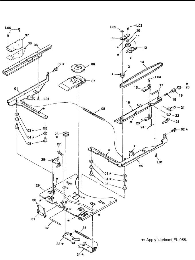
4.4 Loading EX Ass’y ADJ-3 (B02)
Fig.4-4
17

MECHANICAL ASS’Y AND PARTS LIST
4.4 Loading EX Ass’y ADJ-3 (B02)
Ref. No. |
Part No. |
Description |
Q'ty |
B02 |
CA09505A |
Loadig EX Ass’y ADJ-3 |
1 |
01 |
0C10201A |
Loading Plate R SL |
1 |
02 |
0C10215A |
LP Slider SL |
2 |
03 |
0C10295A |
Loading Roller |
4 |
04 |
0C10296A |
Screw Collar |
4 |
05 |
0C10294A |
Loading Screw |
4 |
06 |
CA09403A |
Clamper ADT Ass’y |
1 |
07 |
0C10203A |
Disc Guide Upper SL |
1 |
08 |
0C10252A |
Loading Return Spring SL |
1 |
09 |
CA09356A |
Loading Link B SL S Ass’y |
1 |
10 |
0C10248A |
Loading Idler Gear L SL |
1 |
11 |
0C10247A |
Loading Gear Collar SL |
1 |
12 |
CA09355A |
Loading Link A SL S Ass’y |
1 |
13 |
0C10213A |
Timing Gear SL |
1 |
14 |
0C10190A |
Timing Belt SL |
1 |
15 |
CA09335A |
Disc Fin Arm LO SL S Ass’y |
1 |
16 |
0C10199A |
Disc Guide L SL |
1 |
17 |
0C10214A |
Catch Arm Spring SL |
1 |
18 |
0C10193A |
Pulley Spring SL |
1 |
19 |
0C10192A |
Pulley Fork SL |
1 |
20 |
0C10191A |
Idler Pulley SL |
1 |
21 |
0C10195B |
Lapping Arm SL |
2 |
22 |
0C10194A |
Disc Catch Gear SL |
1 |
23 |
CA09336A |
Disc Fin Arm SL S Ass’y |
1 |
24 |
0C10196C |
Lapping Arm Spring |
1 |
25 |
CA09337A |
Loading Plate L SL A Ass’y |
1 |
26 |
0C10251A |
Loading Center Gear SL |
1 |
27 |
0C10250A |
Shutter Spring SL |
1 |
28 |
0C10204A |
Shutter Lever SL |
1 |
29 |
CA09361A |
Loading Chassis SL S Ass’y |
1 |
30 |
0C10255A |
Shutter Arm Cushion SL |
2 |
31 |
0C10249A |
Shutter Arm SL |
1 |
32 |
0C10254A |
Shutter Arm Shaft SL |
1 |
33 |
0C10206A |
Clamp Holder R SL |
1 |
34 |
0C10205A |
Clamp Holder L SL |
1 |
35 |
0C10253A |
Clamper Return Spring SL |
1 |
36 |
CA09395B |
Disc Guide R EX S Ass’y |
1 |
37 |
0C10581A |
D Guide R side EX |
1 |
38 |
0C10582A |
D Guide Sheet EX |
1 |
L01 |
0E03961A |
BT2x4+Pan (#0 Type 1) (Black) |
|
L02 |
0E03955A |
Cut Washer 2.2x4.2x0.2 |
|
L03 |
0E03969A |
M1.4x3+Pan (#0 Type 3) |
|
L04 |
0E03963A |
BT1.7x3+Pan (#0 Type 1) (Black) |
|
L05 |
0E00793A |
BT2x6+Pan |
|
Apply FL-955 (grease) to the following places (marked with ) when parts are replaced.
Ref. No. |
Location |
Remarks |
01 |
Loading Plate R SL |
Groove |
02 |
LP Slider SL |
Whole surface (2 places) |
03 |
Loading Roller |
Whole surface (4 places) |
04 |
Screw Collar |
Whole surface (4 places) |
09 |
Loading Link B SL S Ass’y |
Gear surface |
10 |
Loading Idler Gear L SL |
Gear surface |
12 |
Loading Link A SL S Ass’y |
Gear surface |
13 |
Timing Gear SL |
Gear surface |
16 |
Disc Guide L SL |
Stud |
20 |
Idler Pulley SL |
Whole surface |
25 |
Loading Plate L SL A Ass’y |
Grooves (2 places) |
26 |
Loading Center Gear SL |
Whole surface |
29 |
Loading Chassis SL S Ass’y |
Holes (4 places) |
33 |
Clamp Holder R SL |
Whole surface |
34 |
Clamp Holder L SL |
Whole surface |
18
MECHANICAL ASS’Y AND PARTS LIST
4.5 DVD Traverse Ass’y ADJ-3 (B03)
: Apply lubricant PG-663
Apply PG-663
19: Gear and Gear Top
|
|
|
|
|
|
|
|
Lubricant: |
|
|
|
|
|
|
|
|
|
We suggest that you use PG-663 or |
|
|
|
|
|
|
|
|
|
equivalent type. |
|
|
|
|
|
|
|
|
|
Please contact: |
|
|
|
|
|
|
|
|
|
Dowcorning Co., Ltd. |
|
|
|
|
|
|
|
|
|
1-1-3 Marunouchi, Chiyoda-ku, |
|
|
|
|
|
Fig.4-5 |
|
Tokyo, Japan |
|
||
4.5 DVD Traverse Ass’y ADJ-3 (B03) |
|
|
|
|
|
|
|
||
|
|
|
|
|
|
|
|||
Ref. No. |
Part No. |
Description |
Q'ty |
|
|
Ref. No. |
Part No. |
Description |
Q'ty |
B03 |
CA09479A |
DVD Traverse Ass’y ADJ-3 |
|
13 |
0C10537A |
Holder Shaft 1 |
1 |
||
01 |
0C10559A |
Holder Shaft 3 |
1 |
14 |
CA09487A |
Shaft Screw Ass’y |
1 |
||
02 |
0C10532A |
Shaft R |
1 |
15 |
0C10524A |
SP Push L.S |
1 |
||
03 |
0C10534A |
Screw S |
2 |
16 |
0C10539A |
Holder Motor |
1 |
||
04 |
0C10525A |
SP Push Shaft |
3 |
17 |
0C10530A |
Traverse-P Chassis |
1 |
||
05 |
0C10536A |
Holder SP |
2 |
18 |
0B90969A |
M. CDS8A50T30-A/TT |
1 |
||
06 |
0C10558A |
Holder SP 2 |
1 |
19 |
CA09488A |
Sled Motor Ass’y |
1 |
||
07 |
0C10531A |
Shaft L |
1 |
20 |
0B70304A |
Switch MPU10420MLB0 |
1 |
||
08 |
0B85437A |
30P Flexible wire (Pickup) |
1 |
21 |
0B85699A |
2P Wire Ass’y L100 |
1 |
||
|
(Note: Do not included in the DVD Traverse Ass’y (CA09479A). |
|
|
L01 |
0E04250A |
ST2x5+Pan CMT |
|
||
09 |
0C10583A |
Cushion PU 7x4x2.5 |
1 |
|
|
L02 |
0E04256A |
M2x4+Pan BNI |
|
10 |
0B90967A |
Pick-up VED0383-AK |
1 |
|
|
L03 |
0E04248A |
M1.7x3.5+Pan CMT |
|
11 |
0C10526A |
SP Push Hook |
1 |
|
|
L04 |
0E04248A |
M1.7x3.5+Pan CMT |
|
12 |
0C10535A |
Hook L.S |
1 |
|
|
L05 |
0E04249A |
ST2x8+Binding CMT |
|
|
|
|
|
|
|
L06 |
0E04247A |
M1.7x2.5+Pan BZN |
|
19

MECHANICAL ASS’Y AND PARTS LIST
4.6 Pakage Ass’y and Accessory Ass’y
2
1
4.6 Pakage Ass’y and Accessory Ass’y
Ref. No. |
Part No. |
Description |
Q'ty |
1 |
0F05622B |
Carton Box |
1 |
2 |
0F05623B |
Packing |
2 |
3 |
0F04458A |
Sheet |
1 |
--- |
0B85744A |
Code YAF11-0642 (UK/EP) |
1 |
--- |
0B85745A |
Code R-C275VP (JPN/OTR/AUS 1 |
|
|
|
/USA/CAN/CH/DA/HK/KR/TW) |
|
--- |
0B90451A |
Batery UM3X1 |
2 |
--- |
0D03092B |
Poly Bag |
1 |
--- |
0F04860A |
Poly Bag (UK/HK only) |
1 |
--- |
0D07238A |
AC Cord UL (USA/CAN) |
1 |
--- |
0D07239A |
AC Cord EP (EP) |
1 |
--- |
0D07240A |
AC Cord DA/DU (DA/OTR/TW) |
1 |
--- |
0D07241A |
AC Cord DM (JPN) |
1 |
--- |
0D07242A |
AC Cord BS/HK (UK/HK) |
1 |
Accessory Ass'y
2
3
Fig.4-6
Ref. No. |
Part No. |
Description |
Q'ty |
--- |
0D07243A |
AC Cord CH (CH) |
1 |
--- |
0D07244A |
AC Cord KR (KR) |
1 |
--- |
0D07245A |
AC Cord SA (AUS) |
1 |
--- |
0D07355A |
Owner’s Manual Japanise (JPN) |
1 |
--- |
0D07356A |
Owner’s Manual English |
1 |
|
|
(Except JPN) |
|
--- |
0D07357A |
Owner’s Manual Franch |
1 |
|
|
(USA/CAN/EP) |
|
--- |
0D07358A |
Owner’s Manual German (EP) |
1 |
--- |
0D07359A |
Owner’s Manual Spanish |
1 |
|
|
(USA/CAN/EP/DA) |
|
--- |
0D07360A |
Owner’s Manual Italian (EP) |
1 |
--- |
0H08216A |
CD Single Adaptor (JPN) |
1 |
--- |
HG08343A |
Remote Control Unit |
1 |
20
5. ELECTRICAL PARTS LIST
Notes:
1.Abbreviations
TR-Transistor, SID-Slicon Diode, ZD-Zener Diode,
RC-Cement Resistor, RF-Fail Safe Type Resistor,
RK-Carbon Resistor.
IC-Integrated Circuit, CML-Mylar Capacitor,
CC-Ceramic Capacitor, CE-Electrolytic Capacitor.
2.Parts marked with * show chip parts.
5.1 Mechanism P.C.B. Ass’y (C3M1)
Ref. No. |
Part No. |
|
Description |
Q'ty |
|
BA10323A |
|
Mech P.C.B. Ass’y C3M1 |
|
CN100 |
0B85425A |
|
40P F Connector* |
1 |
CN200 |
0B85424A |
|
30P F Connector* |
1 |
CN300 |
0B85420A |
|
11P F Connector* |
1 |
CN501 |
0B80941A |
|
14P F Connector * |
1 |
CP103 |
0B84785A |
|
22P F Connector* |
1 |
CP502 |
0B85421A |
|
13P F Connector* |
1 |
D011 |
0B12249A |
SID |
1SS133 |
1 |
D031,032 |
0B12249A |
SID |
1SS133 |
2 |
D404 |
0B10540A |
SID |
MA152WA* |
1 |
D406 |
0B10540A |
SID |
MA152WA* |
1 |
D516 |
0B10539A |
SID |
MA152WK* |
1 |
D518 |
0B12249A |
SID |
1SS133 |
1 |
ICP01 |
0B12918A |
IC |
ICP 0.5A* |
1 |
Q001 |
0B14013A |
TR |
DTC144EK* |
1 |
Q031,032 |
0B12901A |
TR |
2SB1132R * |
2 |
Q033,034 |
0B14227A |
TR |
2SA1576 S * |
2 |
Q035 |
0B14188A |
TR |
2SC4081 R * |
1 |
Q036 |
0B10882A |
TR |
DTC114TKA* |
1 |
Q037 |
0B14188A |
TR |
2SC4081 R * |
1 |
Q038 |
0B14002A |
TR |
DTA114EK* |
1 |
Q090 |
0B14167A |
TR |
2SC2412K * |
1 |
Q401 |
0B10792A |
TR |
2SB1182QR* |
1 |
Q402 |
0B14167A |
TR |
2SC2412K * |
1 |
Q403 |
0B10901A |
TR |
2SD2153TL* |
1 |
Q404 |
0B10930A |
TR |
2SD1758F * |
1 |
Q411,412 |
0B14167A |
TR |
2SC2412K * |
2 |
Q501 |
0B14167A |
TR |
2SC2412K * |
1 |
Q502 |
0B14013A |
TR |
DTC144EK* |
1 |
Q511,512 |
0B14018A |
TR |
DTC143TK* |
2 |
Q513,514 |
0B14018A |
TR |
DTC143TK* |
2 |
Q515 |
0B14018A |
TR |
DTC143TK* |
1 |
U001 |
0B12868A |
IC |
BA6859AFP* |
1 |
U002 |
0B12867A |
IC |
BA5938FM* |
1 |
U003 |
0B11001A |
IC |
NJM4558M |
1 |
U004 |
0B06404A |
IC |
NJM2904M |
1 |
U105,106 |
0B10719A |
IC |
TA8409F * |
2 |
U107,108 |
0B10719A |
IC |
TA8409F * |
2 |
U401 |
0B10566A |
IC |
PQ09RF1 |
1 |
U501 |
0B13256A |
IC |
HD6433396F* |
1 |
U502 |
0B11928A |
IC |
TC4049BF |
1 |
X501 |
0B90740A |
|
Resonator 6.00MHz |
1 |
Ref. No. |
Part No. |
|
Description |
Q'ty |
ZD033 |
0B12168A |
ZD |
RD10V JS B2 |
1 |
ZD401 |
0B12150A |
ZD |
RD5.6V JS B2 |
1 |
ZD402 |
0B12160A |
ZD |
RD7.5V JS B3 |
1 |
ZD403 |
0B12153A |
ZD |
RD6.2V JS B2 |
1 |
ZD404 |
0B12150A |
ZD |
RD5.6V JS B2 |
1 |
ZD502,503 |
0B12154A |
ZD |
RD6.2V JS B3 |
2 |
21

ELECTRICAL PARTS LIST
5.2 DVD Main P.C.B. Ass’y (C3M1)
Ref. No. |
Part No. |
|
Description |
Q'ty |
|
BK10567A |
|
DVD Main P.C.B. Ass’y C3M1 |
|
D101,102 |
0B13151A |
SID |
1SS355TE-17* |
2 |
D103 |
0B13151A |
SID |
1SS355TE-17* |
1 |
D120 |
0B13151A |
SID |
1SS355TE-17* |
1 |
D190 |
0B13151A |
SID |
1SS355TE-17* |
1 |
D191 |
0B13152A |
SID |
DA204U-T106* |
1 |
D193 |
0B13151A |
SID |
1SS355TE-17* |
1 |
D209 |
0B13151A |
SID |
1SS355TE-17* |
1 |
D300,301 |
0B13151A |
SID |
1SS355TE-17* |
2 |
D500,501 |
0B13151A |
SID |
1SS355TE-17* |
2 |
D850 |
0B13153A |
SID |
UMN11N-TN* |
1 |
D901 |
0B13153A |
SID |
UMN11N-TN* |
1 |
D902,903 |
0B13151A |
SID |
1SS355TE-17* |
2 |
IC100 |
0B13171A |
IC |
CYC11AP000* |
1 |
IC110,111 |
0B13179A |
IC |
NJM4558M* |
2 |
IC120 |
0B13169A |
IC |
BU4011BFV-E2* |
1 |
IC121,122 |
0B13170A |
IC |
BU4S81-TR* |
2 |
IC201 |
0B13172A |
IC |
CYC12MP000* |
1 |
IC202 |
0B13190A |
IC |
TC7SHU04FU* |
1 |
IC203 |
0B13179A |
IC |
NJM4558M* |
1 |
IC300 |
0B13177A |
IC |
MN67700VRZB* |
1 |
IC311 |
0B13190A |
IC |
TC7SHU04FU* |
1 |
IC410,411 |
0B13178A |
IC |
NJM2903V* |
2 |
IC412 |
0B13169A |
IC |
BU4011BFV-E2* |
1 |
IC490 |
0B13165A |
IC |
MN66261 |
1 |
IC500 |
0B13173A |
IC |
CYC13DD000* |
1 |
IC501 |
0B13175A |
IC |
HY628100ALG-55* |
1 |
IC502 |
0B13174A |
IC |
HY57V161610DTC* |
1 |
IC503 |
0B13183A |
IC |
TC74VHC00FT* |
1 |
IC507 |
0B13186A |
IC |
TC74VHC32FTEL* |
1 |
IC550 |
0B13185A |
IC |
TC74VHC157FTEL* |
1 |
IC600 |
BA10572A |
|
DVD AK-SYS6 KIT |
1 |
IC602 |
BA10573A |
|
OPT ROM NC100503 KIT |
1 |
IC603 |
0B13176A |
IC |
M24C16-MN6T* |
1 |
IC605 |
0B13183A |
IC |
TC74VHC00FT* |
1 |
IC606 |
0B13189A |
IC |
TC74VHCT245AFT* |
1 |
IC607 |
0B13187A |
IC |
TC74VHC574FTEL* |
1 |
IC610 |
0B13191A |
IC |
TC7W04FUTE12L* |
1 |
IC611 |
0B13183A |
IC |
TC74VHC00FT* |
1 |
IC612 |
0B13193A |
IC |
TC7WH74FUTE12L* |
1 |
IC613 |
0B13184A |
IC |
TC74VHC08FTEL* |
1 |
IC614 |
0B13188A |
IC |
TC74VHC86FT* |
1 |
IC700 |
0B13195A |
IC |
ZIVA-3-PEO* |
1 |
IC701,702 |
0B13174A |
IC |
HY57V161610DTC* |
2 |
IC703 |
0B13192A |
IC |
TC7WH157FU* |
1 |
IC704 |
0B13181A |
IC |
SI-3025ALS-TL* |
1 |
IC800 |
0B13182A |
IC |
SM8701BM-ET* |
1 |
IC801 |
0B13194A |
IC |
TC7WU04FUTE12L* |
1 |
IC802 |
0B13190A |
IC |
TC7SHU04FU* |
1 |
IC803 |
0B13194A |
IC |
TC7WU04FUTE12L* |
1 |
IC850 |
0B13167A |
IC |
ADV7172 KST* |
1 |
IC901 |
0B13168A |
IC |
BA05FP-E2* |
1 |
IC911 |
0B13180A |
IC |
PCM1735E/2K* |
1 |
IC991 |
0B13231A |
IC |
TC74HC4053AFT* |
1 |
Ref. No. |
Part No. |
|
Description |
Q'ty |
P800 |
0B85696A |
|
SO 40FLT-SM1-TB* |
1 |
P803 |
0B85694A |
|
FFC 24FLT-SM1-TB* |
1 |
P807 |
0B85697A |
|
SO S06B-XH-SM3-TB* |
1 |
P999 |
0B85695A |
|
SO 10FM-1.0-SP1.9* |
1 |
TR100,101 |
0B13161A |
TR |
UMG4N-TR* |
2 |
TR102,103 |
0B13161A |
TR |
UMG4N-TR* |
2 |
TR104,105 |
0B13161A |
TR |
UMG4N-TR* |
2 |
TR106 |
0B13161A |
TR |
UMG4N-TR* |
1 |
TR110,111 |
0B13163A |
TR |
2SK880-TE85L* |
2 |
TR112 |
0B13162A |
TR |
2SK2145-TE85L* |
1 |
TR115 |
0B13157A |
TR |
UMY3N-TR* |
1 |
TR117 |
0B13160A |
TR |
DTC144TUA* |
1 |
TR120 |
0B13155A |
TR |
UMW1N-TR* |
1 |
TR125 |
0B13160A |
TR |
DTC144TUA* |
1 |
TR167 |
0B13154A |
TR |
FMY4A-T148* |
1 |
TR170 |
0B13160A |
TR |
DTC144TUA* |
1 |
TR171 |
0B13156A |
TR |
UMX3N-TR* |
1 |
TR172 |
0B13196A |
TR |
2SA1576A-Q/R/S* |
1 |
TR190 |
0B13159A |
TR |
DTC144EUA* |
1 |
TR200,201 |
0B13197A |
TR |
2SC4081-R/S* |
2 |
TR202 |
0B13197A |
TR |
2SC4081-R/S* |
1 |
TR300 |
0B13158A |
TR |
DTA144EUA* |
1 |
TR490 |
0B13159A |
TR |
DTC144EUA* |
1 |
TR491 |
0B13160A |
TR |
DTC144TUA* |
1 |
TR500 |
0B13160A |
TR |
DTC144TUA* |
1 |
TR600 |
0B13159A |
TR |
DTC144EUA* |
1 |
TR801,802 |
0B13196A |
TR |
2SA1576A-Q/R/S* |
2 |
TR804,805 |
0B13196A |
TR |
2SA1576A-Q/R/S* |
2 |
TR806 |
0B13196A |
TR |
2SA1576A-Q/R/S* |
1 |
VR110 |
0B30229A |
|
Semi VR 22K* |
1 |
VR120,121 |
0B30229A |
|
Semi VR 22K* |
2 |
X301 |
0B90966A |
|
X’tal CX-16F 40MHz* |
1 |
X601 |
0B90964A |
|
X’tal CCR4.0MC3T* |
1 |
X800 |
0B90965A |
|
X’tal CX-11F 27MH* |
1 |
22

ELECTRICAL PARTS LIST
5.3 Digital P.C.B. Ass’y
Ref. No. |
Part No. |
Description |
Q'ty |
|
BK10258A |
Digital P.C.B. Ass’y (USA/CAN) |
|
|
BK10562A |
Digital P.C.B. Ass’y (JPN) |
|
|
BK10563A |
Digital P.C.B. Ass’y (EP/UK) |
|
|
BK10564A |
Digital P.C.B. Ass’y Other NTSC |
|
|
BK10566A |
Digital P.C.B. Ass’y Other PAL |
|
C226 |
0B41298A CML |
0.1 50V J (EP/UK only) |
1 |
C227 |
0B41298A CML |
0.1 50V J (EP/UK only) |
1 |
C397 |
0B43203A CC |
330P 50V J* (EP/UK only) |
1 |
C701 |
0B42342A CE |
0.1F 5.5V |
1 |
J300 |
0B12811A |
Toslink TOTX178A |
1 |
L300 |
0B51351A |
Pulse Transformer (TC-1027-04) |
1 |
PJ200 |
0B85644A |
8P Pin Jack R/W |
1 |
PJ300 |
0B85645A |
1P Pin Jack ORG |
1 |
PJ400 |
0B85576A |
ST Mini Jack |
1 |
SW300 |
0B70296A |
Slide SW |
1 |
X101 |
0B90902A |
X’tel 12.288MHz |
1 |
X500 |
0B91047A |
X’tal 8.38MHz |
1 |
D200,201 |
0B12835A SID |
1SS355* |
2 |
D202,203 |
0B12835A SID |
1SS355* |
2 |
D204,205 |
0B12835A SID |
1SS355* |
2 |
D206,207 |
0B12835A SID |
1SS355* |
2 |
D208,209 |
0B12835A SID |
1SS355* |
2 |
D210,211 |
0B12835A SID |
1SS355* |
2 |
D212 |
0B12835A SID |
1SS355* |
1 |
D690,691 |
0B12586A SID |
1N4002 |
2 |
D692,693 |
0B12835A SID |
1SS355* |
2 |
D694,695 |
0B12835A SID |
1SS355* |
2 |
D696,697 |
0B12835A SID |
1SS355* |
2 |
D698 |
0B12586A SID |
1N4002 |
1 |
IC101 |
0B12885A IC |
YSS912* |
1 |
IC103 |
0B12883A IC |
LC89055W* |
1 |
IC104 |
0B11603A IC |
TC74HCU04AF |
1 |
IC105 |
0B11613A IC |
TC74HC00AF |
1 |
IC200,201 |
0B14189A IC |
UPC4570G2* |
2 |
IC202,203 |
0B14189A IC |
UPC4570G2* |
2 |
IC204,205 |
0B14189A IC |
UPC4570G2* |
2 |
IC206,207 |
0B14189A IC |
UPC4570G2* |
2 |
IC208,209 |
0B14189A IC |
UPC4570G2* |
2 |
IC210,211 |
0B14189A IC |
UPC4570G2* |
2 |
IC212,213 |
0B14189A IC |
UPC4570G2* |
2 |
IC214 |
0B14189A IC |
UPC4570G2* |
1 |
IC215 |
0B10812A IC |
LC78211 |
1 |
IC216 |
0B10814A IC |
LC78213 |
1 |
IC217 |
0B10813A IC |
LC78212 |
1 |
IC218,219 |
0B14189A IC |
UPC4570G2* |
2 |
IC220,221 |
0B14189A IC |
UPC4570G2* |
2 |
IC222,223 |
0B14189A IC |
UPC4570G2* |
2 |
IC224,225 |
0B14189A IC |
UPC4570G2* |
2 |
IC390 |
0B11613A IC |
TC74HC00AF |
1 |
IC401,402 |
0B12783A IC |
AD1855* |
2 |
IC403 |
0B12783A IC |
AD1855* |
1 |
IC404,405 |
0B14189A IC |
UPC4570G2* |
2 |
IC406 |
0B14189A IC |
UPC4570G2* |
1 |
IC500 |
0B12863A IC |
UPD78F4225GC-8* |
1 |
P530 |
0B85929A |
13P F Connector* |
1 |
Ref. No. |
Part No. |
Description |
Q'ty |
P550 |
0B85930A |
14P F Connector* |
1 |
P570 |
0B85829A |
24P F Connector* |
1 |
P600 |
0B85931A |
17P F Connector* |
1 |
R578 |
0B25579A RK |
47K 1/10W J* (UK/EP/DA/KR/TW) 1 |
|
R579 |
0B25579A RK |
47K 1/10W J* (UK/USA/CAN/EP) 1 |
|
R580 |
0B25579A RK |
47K 1/10W J* (JPN) |
1 |
R678 |
0B25579A RK |
47K 1/10W J* |
1 |
|
|
(JPN/OTR/AUS/USA/CAN/CH/HK) |
|
R679 |
0B25579A RK |
47K 1/10W J* (Except USA/CAN) 1 |
|
R680 |
0B25579A RK |
47K 1/10W J* (Except JPN) |
1 |
TR200,201 |
0B06299A TR |
2SC2878 |
2 |
TR202,203 |
0B06299A TR |
2SC2878 |
2 |
TR204,205 |
0B06299A TR |
2SC2878 |
2 |
TR206,207 |
0B06299A TR |
2SC2878 |
2 |
TR208 |
0B06299A TR |
2SC2878 |
1 |
TR209 |
0B14002A TR |
DTA114EK* |
1 |
TR211 |
0B14002A TR |
DTA114EK* |
1 |
TR213 |
0B14002A TR |
DTA114EK* |
1 |
TR215 |
0B14002A TR |
DTA114EK* |
1 |
TR217 |
0B14002A TR |
DTA114EK* |
1 |
TR218,219 |
0B14167A TR |
2SC2412K * |
2 |
TR220,221 |
0B14167A TR |
2SC2412K * |
2 |
TR222 |
0B14167A TR |
2SC2412K * |
1 |
TR301,302 |
0B14011A TR |
DTC114EK* |
2 |
TR690 |
0B14167A TR |
2SC2412K * |
1 |
TR691 |
0B14002A TR |
DTA114EK* |
1 |
L472 |
0B25612A |
RK 0 1/10W J* (UK/EP) |
1 |
|
0B50467A |
Coil 100uH* (Except UK/EP) |
1 |
23

ELECTRICAL PARTS LIST
5.4 Output P.C.B. Ass’y
Ref. No. |
Part No. |
|
Description |
Q'ty |
|
BK10255A |
|
Output P.C.B. Ass’y (Except UK/EP/JPN) |
|
|
BK10377A |
|
Output P.C.B. Ass’y (JPN) |
|
|
BK10378A |
|
Output P.C.B. Ass’y (EP/UK) |
|
IC100 |
0B11146A |
IC |
TC4053BP (UK/EP) |
1 |
IC101 |
0B12995A |
IC |
BA7666FS* |
1 |
IC102 |
0B12862A |
IC |
BA7660FS* |
1 |
IC500 |
0B12864A |
IC |
PQ30RV2 |
1 |
IC510 |
0B10554A |
IC |
PQ05RF1 |
1 |
IC530 |
0B10554A |
IC |
PQ05RF1 |
1 |
IC540 |
0B12791A |
IC |
PQ20VZ1U* |
1 |
IC570 |
0B11751A |
IC |
NJM7815FA |
1 |
IC580 |
0B11752A |
IC |
NJM7915FA |
1 |
PJ100 |
0B85646A |
|
2P Pin Jack YEL |
1 |
PJ101 |
0B85647A |
|
3P Pin Jack G/B/R (Except EP/UK) |
1 |
PJ102 |
0B90953A |
|
S-Video Jack |
1 |
PJ103 |
0B85631A |
|
21P Connector (EP/UK only) |
1 |
D100 |
0B12154A |
ZD |
RD6.2V JS B3 (EP/UK only) |
1 |
D101 |
0B12175A |
ZD |
RD12JSB3 (EP/UK only) |
1 |
D502 |
0B12249A |
SID |
1SS133 |
1 |
D521 |
0B10520A |
SID |
GBU6D |
1 |
TR100,101 |
0B10026A |
TR |
2SA933S |
2 |
TR102 |
0B10026A |
TR |
2SA933S |
1 |
TR103,104 |
0B10039A |
TR |
2SC1740S(SE) |
2 |
TR105 |
0B10039A |
TR |
2SC1740S(SE) |
1 |
TR106 |
0B10026A |
TR |
2SA933S (EP/UK only) |
1 |
TR107,108 |
0B10026A |
TR |
2SA933S |
2 |
TR109 |
0B10039A |
TR |
2SC1740S(SE) (EP/UK only) |
1 |
TR110,111 |
0B10039A |
TR |
2SC1740S(SE) |
2 |
TR112,113 |
0B10039A |
TR |
2SC1740S(SE) |
2 |
TR114 |
0B12991A |
TR |
DTC143ZS (JPN only) |
1 |
TR115 |
0B12991A |
TR |
DTC143ZS (EP/UK only) |
1 |
TR116 |
0B12991A |
TR |
DTC143ZS (EP/UK only) |
1 |
TR117 |
0B10026A |
TR |
2SA933S (EP/UK only) |
1 |
TR118 |
0B12991A |
TR |
DTC143ZS (EP/UK only) |
1 |
TR119 |
0B10039A |
TR |
2SC1740S(SE) (EP/UK only) |
1 |
TR490 |
0B06299A |
TR |
2SC2878 (EP/UK only) |
1 |
TR491 |
0B06299A |
TR |
2SC2878 (EP/UK only) |
1 |
5.5 Front P.C.B. Ass’y
Ref. No. |
Part No. |
|
Description |
Q'ty |
|
BK10253A |
|
Front P.C.B. Ass’y |
|
IC601 |
0B12866A |
IC |
LC75874E * |
1 |
IC602 |
0B12993A |
IC |
NJU3716L |
1 |
IN601 |
0B90957A |
|
LCD |
1 |
PH601 |
0B12999A |
|
Photo Sensor |
1 |
D601,602 |
0B12998A |
|
LED Amber/Green |
2 |
D603,604 |
0B12998A |
|
LED Amber/Green |
2 |
D605 |
0B12998A |
|
LED Amber/Green |
1 |
D607,608 |
0B12996A |
|
LED Amber |
2 |
D609,610 |
0B12996A |
|
LED Amber |
2 |
D611,612 |
0B13385A |
|
LED Amber (605NM) |
2 |
Ref. No. |
Part No. |
Description |
Q'ty |
D613,614 |
0B13385A |
LED Amber (605NM) |
2 |
SW601,602 |
0B70298A |
Tact SW |
2 |
SW603,604 |
0B70298A |
Tact SW |
2 |
SW605,606 |
0B70298A |
Tact SW |
2 |
SW607,608 |
0B70298A |
Tact SW |
2 |
SW609,610 |
0B70298A |
Tact SW |
2 |
SW611,612 |
0B70298A |
Tact SW |
2 |
TR601 |
0B10969A TR |
DTD113ZK* |
1 |
5.6 Head phone P.C.B. Ass’y
Ref. No. |
Part No. |
Description |
Q'ty |
|
BK10254A |
HP P.C.B. Ass’y (Except EP/UK) |
|
|
BK10574A |
HP P.C.B. Ass’y (EP/UK) |
|
C811 |
0B41298A CML |
0.1 50V J (EP/UK) |
1 |
C812 |
0B41298A CML |
0.1 50V J (EP/UK) |
1 |
IC801 |
0B10743A IC |
NJM4556D |
1 |
PJ801 |
0B85642A |
3P Mini Jack 6.3 |
1 |
VR801 |
0B30228A |
VR 50K(A)x2 L25 |
1 |
TR801,802 |
0B06299A TR |
2SC2878 |
2 |
5.7 P-Supply P.C.B. Ass’y
Ref. No. |
Part No. |
Description |
Q'ty |
|
BK10269A |
P Supply P.C.B. Ass’y (USA/CAN) |
|
|
BK10379A |
P Supply P.C.B. Ass’y (JPN) |
|
|
BK10380A |
P Supply P.C.B. Ass’y (OTR/DA) |
|
|
BK10381A |
P Supply P.C.B. Ass’y (EP/UK) |
|
|
BK10382A |
P Supply P.C.B. Ass’y (AUS/CH/HK/KR) |
|
|
BK10383A |
P Supply P.C.B. Ass’y (TW) |
|
F701 |
0B91083A |
Fuse 3.15A-250V |
1 |
IC701 |
0B17033A IC |
NJM78M12FA |
1 |
IC702 |
0B12994A IC |
PQ30RV1 |
1 |
P701 |
0B85361A |
AC Inlet (USA/CAN) |
1 |
|
0B85362A |
AC Inlet (Except USA/CAN) |
1 |
RL701 |
0B90907A |
Relay OSZ-SH-112DM |
1 |
T701 |
0B50342A |
Sub Transformer (USA/CAN/JPN) 1 |
|
|
0B50343A |
Sub Transformer |
1 |
|
|
(Except USA/CAN/JPN) |
|
C715 |
0B41298A CML |
0.1 50V J (EP/UK) |
1 |
D701,702 |
0B12586A SID |
1N4002 |
2 |
D703,704 |
0B12249A SID |
1SS133 |
2 |
D705 |
0B12249A SID |
1SS133 |
1 |
TR701 |
0B12992A TR |
DTC113ZKA* |
1 |
TR702,703 |
0B14167A TR |
2SC2412K * |
2 |
24

ELECTRICAL PARTS LIST
5.8 M-Trans P.C.B. Ass’y
Ref. No. |
Part No. |
Description |
Q'ty |
|
BK10376A |
M Trans P.C.B. Ass’y |
|
D500,501 |
0B12586A SID |
1N4002 |
2 |
D510,511 |
0B12586A SID |
1N4002 |
2 |
F201,202 |
0B91091A |
Fuse 4A-125V |
2 |
F203,204 |
0B91088A |
Fuse 7A-125V |
2 |
F205,206 |
0B91089A |
Fuse 3A-125V |
2 |
F207,208 |
0B91084A |
Fuse 1A-125V |
2 |
5.9 Power SW P.C.B. Ass’y
Ref. No. |
Part No. |
Description |
Q'ty |
|
BK10268A |
Power SW P.C.B. Ass’y |
|
SW301 |
0B70292A |
Power SW |
1 |
5.10 LED P.C.B. Ass’y
Ref. No. |
Part No. |
Description |
Q'ty |
|
BK10257A |
LED P.C.B. Ass’y |
|
D401 |
0B12998A |
LED Amber/Green |
1 |
5.11 Diode P.C.B. Ass’y
Ref. No. |
Part No. |
Description |
Q'ty |
|
BK10565A |
DIODE P.C.B. Ass’y |
|
D520 |
0B10543A SID |
GBU8D |
1 |
5.12 REG. 3V P.C.B. Ass’y
Ref. No. |
Part No. |
Description |
Q'ty |
|
BK10557A |
REG3V P.C.B. Ass’y |
|
IC560 |
0B12994A IC |
PQ30RV1 |
1 |
5.13 REG. 5V P.C.B. Ass’y
Ref. No. |
Part No. |
Description |
Q'ty |
|
BK10556A |
REG5V P.C.B. Ass’y |
|
IC550 |
0B10554A IC |
PQ05RF1 |
1 |
5.14 Mecha Flexible P.C.B. Ass’y
Ref. No. |
Part No. |
|
Description |
Q'ty |
|
BA09736A |
|
Mecha Flexible P.C.B. ASS’y |
|
PC701,702 |
0B10737A |
IC |
PhotoInterrupter |
2 |
PC703,704 |
0B10737A |
IC |
PhotoInterrupter |
2 |
PC705,706 |
0B10737A |
IC |
PhotoInterrupter |
2 |
PC707,708 |
0B10737A |
IC |
PhotoInterrupter |
2 |
PC709 |
0B10737A |
IC |
PhotoInterrupter |
1 |
5.15 Photo P.C.B. Ass’y
Ref. No. |
Part No. |
Description |
Q'ty |
|
BA10175A |
Photo P.C.B. Ass’y |
|
|
0B10737A IC |
PhotoInterrupter |
1 |
25

6. RECOMMENDED SPARE PARTS LIST
Notes:
1.Abbreviations
TR-Transistor, SID-Slicon Diode, ZD-Zener Diode,
RC-Cement Resistor, RF-Fail Safe Type Resistor,
RK-Carbon Resistor.
IC-Integrated Circuit, CML-Mylar Capacitor,
CC-Ceramic Capacitor, CE-Electrolytic Capacitor.
2.Parts marked with * show chip parts.
Ref. No. |
Part No. |
|
Description |
1 |
0B06404A |
IC |
NJM2904M |
2 |
0B10554A |
IC |
PQ05RF1 |
3 |
0B10566A |
IC |
PQ09RF1 |
4 |
0B10719A |
IC |
TA8409F * |
5 |
0B10737A |
IC |
PhotoInterrupter |
6 |
0B10743A |
IC |
NJM4556D |
7 |
0B10812A |
IC |
LC78211 |
8 |
0B10813A |
IC |
LC78212 |
9 |
0B10814A |
IC |
LC78213 |
10 |
0B11001A |
IC |
NJM4558M |
11 |
0B11146A |
IC |
TC4053BP |
12 |
0B11603A |
IC |
TC74HCU04AF |
13 |
0B11613A |
IC |
TC74HC00AF |
14 |
0B11751A |
IC |
NJM7815FA |
15 |
0B11752A |
IC |
NJM7915FA |
16 |
0B11928A |
IC |
TC4049BF |
17 |
0B12783A |
IC |
AD1855* |
18 |
0B12791A |
IC |
PQ20VZ1U* |
19 |
0B12862A |
IC |
BA7660FS* |
20 |
0B12863A |
IC |
UPD78F4225GC-8* |
21 |
0B12864A |
IC |
PQ30RV2 |
22 |
0B12866A |
IC |
LC75874E * |
23 |
0B12867A |
IC |
BA5938FM* |
24 |
0B12868A |
IC |
BA6859AFP* |
25 |
0B12883A |
IC |
LC89055W* |
26 |
0B12885A |
IC |
YSS912* |
27 |
0B12918A |
IC |
ICP 0.5A* |
28 |
0B12993A |
IC |
NJU3716L |
29 |
0B12994A |
IC |
PQ30RV1 |
30 |
0B12995A |
IC |
BA7666FS* |
31 |
0B13165A |
IC |
MN66261 |
32 |
0B13167A |
IC |
ADV7172 KST* |
33 |
0B13168A |
IC |
BA05FP-E2* |
34 |
0B13169A |
IC |
BU4011BFV-E2* |
35 |
0B13170A |
IC |
BU4S81-TR* |
36 |
0B13171A |
IC |
CYC11AP000* |
37 |
0B13172A |
IC |
CYC12MP000* |
38 |
0B13173A |
IC |
CYC13DD000* |
39 |
0B13174A |
IC |
HY57V161610DTC* |
40 |
0B13175A |
IC |
HY628100ALG-55* |
41 |
0B13176A |
IC |
M24C16-MN6T* |
42 |
0B13177A |
IC |
MN67700VRZB* |
43 |
0B13178A |
IC |
NJM2903V* |
44 |
0B13179A |
IC |
NJM4558M* |
45 |
0B13180A |
IC |
PCM1735E/2K* |
46 |
0B13181A |
IC |
SI-3025ALS-TL* |
47 |
0B13182A |
IC |
SM8701BM-ET* |
48 |
0B13183A |
IC |
TC74VHC00FT* |
49 |
0B13184A |
IC |
TC74VHC08FTEL* |
50 |
0B13185A |
IC |
TC74VHC157FTEL* |
51 |
0B13186A |
IC |
TC74VHC32FTEL* |
52 |
0B13187A |
IC |
TC74VHC574FTEL* |
53 |
0B13188A |
IC |
TC74VHC86FT* |
54 |
0B13189A |
IC |
TC74VHCT245AFT* |
55 |
0B13190A |
IC |
TC7SHU04FU* |
56 |
0B13191A |
IC |
TC7W04FUTE12L* |
57 |
0B13192A |
IC |
TC7WH157FU* |
58 |
0B13193A |
IC |
TC7WH74FUTE12L* |
59 |
0B13194A |
IC |
TC7WU04FUTE12L* |
60 |
0B13195A |
IC |
ZIVA-3-PEO* |
61 |
0B13231A |
IC |
TC74HC4053AFT* |
Ref. No. |
Part No. |
|
Description |
62 |
0B13256A |
IC |
HD6433396F* |
63 |
0B17033A |
IC |
NJM78M12FA |
64 |
0B10520A |
SID |
GBU6D |
65 |
0B10539A |
SID |
MA152WK* |
66 |
0B10543A |
SID |
GBU8D |
67 |
0B12249A |
SID |
1SS133 |
68 |
0B12586A |
SiD |
1N4002 |
66 |
0B12835A |
SID |
1SS355* |
70 |
0B13151A |
SID |
1SS355TE-17* |
71 |
0B13152A |
SID |
DA204U-T106* |
72 |
0B13153A |
SID |
UMN11N-TN* |
73 |
0B06299A |
TR |
2SC2878 |
74 |
0B10026A |
TR |
2SA933S |
75 |
0B10039A |
TR |
2SC1740S(SE) |
76 |
0B10792A |
TR |
2SB1182QR* |
77 |
0B10882A |
TR |
DTC114TKA* |
78 |
0B10901A |
TR |
2SD2153TL* |
79 |
0B10930A |
TR |
2SD1758F * |
80 |
0B10969A |
TR |
DTD113ZK* |
81 |
0B12901A |
TR |
2SB1132R * |
82 |
0B12991A |
TR |
DTC143ZS |
83 |
0B12992A |
TR |
DTC113ZKA* |
84 |
0B13154A |
TR |
FMY4A-T148* |
85 |
0B13155A |
TR |
UMW1N-TR* |
86 |
0B13156A |
TR |
UMX3N-TR* |
87 |
0B13157A |
TR |
UMY3N-TR* |
88 |
0B13158A |
TR |
DTA144EUA* |
89 |
0B13159A |
TR |
DTC144EUA* |
90 |
0B13160A |
TR |
DTC144TUA* |
91 |
0B13161A |
TR |
UMG4N-TR* |
92 |
0B13162A |
TR |
2SK2145-TE85L* |
93 |
0B13163A |
TR |
2SK880-TE85L* |
94 |
0B13196A |
TR |
2SA1576A-Q/R/S* |
95 |
0B13197A |
TR |
2SC4081-R/S* |
96 |
0B14002A |
TR |
DTA114EK* |
97 |
0B14011A |
TR |
DTC114EK* |
98 |
0B14013A |
TR |
DTC144EK* |
99 |
0B14018A |
TR |
DTC143TK* |
100 |
0B14167A |
TR |
2SC2412K * |
101 |
0B14188A |
TR |
2SC4081 R * |
102 |
0B14227A |
TR |
2SA1576 S * |
103 |
0B12150A |
ZD |
RD5.6V JS B2 |
104 |
0B12153A |
ZD |
RD6.2V JS B2 |
105 |
0B12154A |
ZD |
RD6.2V JS B3 |
106 |
0B12160A |
ZD |
RD7.5V JS B3 |
107 |
0B12168A |
ZD |
RD10V JS B2 |
108 |
0B12175A |
ZD |
RD12JSB3 |
109 |
0B12811A |
|
Toslink TOTX178A |
110 |
0B12999A |
|
Photo Sensor |
111 |
0B50342A |
|
Sub Transformer DM/UL |
112 |
0B50343A |
|
Sub Transformer EP/OTR |
113 |
0B50459A |
|
Power Transformer 100-120V |
114 |
0B50460A |
|
Power Transformer 115-230V |
115 |
0B51351A |
|
Pulse Transformer (TC-1027-04) |
116 |
0B70296A |
|
Slide SW |
117 |
0B70298A |
|
Tact SW |
118 |
0B70300A |
|
Slide SW L21-22A2 |
119 |
0B70304A |
|
Switch MPU10420MLB0 |
120 |
0B90907A |
|
Relay OSZ-SH-112DM |
121 |
0B90967A |
|
Pick-up VED0383-AK |
122 |
0B91083A |
|
Fuse 3.15A-250V |
123 |
0B91084A |
|
Fuse 1A-125V |
124 |
0B91088A |
|
Fuse 7A-125V |
125 |
0B91089A |
|
Fuse 3A-125V |
126 |
0B91091A |
|
Fuse 4A-125V |
127 |
0C10190A |
|
Timing Belt SL |
128 |
CA09479A |
|
DVD Traverse Ass’y ADJ-3 |
26

7. IC BLOCK DIAGRAMS
7.1 AD1855 (A/D Converter) - IC401,402,403 on Digital P.C.B. Ass’y
7.2 ADV7172 (Video signal decoder) - IC850 on DVD Main P.C.B. Ass’y
27

IC BLOCK DIAGRAMS
7.3 BA5938FM (Power driver) - U002 on Mechanism P.C.B. Ass’y
7.4 BA6859AFP (3-Phase motor driver) - U001 on Mchanism P.C.B. Ass’y
28

IC BLOCK DIAGRAMS
7.5 CYC11AP000 (DVD Pre-AMP) - IC100 on DVD Main P.C.B. Ass’y
Pin No. |
Port Name |
I/O |
FUNCTION |
|
|
|
|
1 |
NC |
--- |
No connection. |
|
|
|
|
2,19,23,38,48 |
AVSS |
--- |
Ground pin. |
|
|
|
|
3 |
LPCVREF |
O |
LPC (laser power control) reference voltage output. |
|
|
|
|
4 |
LPCI1 |
I |
LPC (laser power control) non-inverting input pin. |
|
|
|
|
5 |
LPCI2 |
I |
LPC (laser power control) inverting input pin. |
|
|
|
|
6 |
LPCO |
O |
LPC (laser power control) output.. |
|
|
|
|
7 |
LDON |
I |
LPC (laser power control) on/off control (H;LD on, L: LD off). |
|
|
|
|
8 |
FBAL |
I |
Focus balance control input. |
|
|
|
|
9 |
VFEI_P |
I |
Focus AMP positive input pin. |
|
|
|
|
10 |
VFEI_N |
I |
Focus AMP negative input pin. |
|
|
|
|
11 |
FEO |
O |
Focus error output pin. |
|
|
|
|
12 |
FE3XINN |
I |
Focus AMP negative input pin. |
|
|
|
|
13 |
FE3XINP |
I |
Focus AMP positive input pin. |
|
|
|
|
14 |
VFE2N4 |
O |
Vin2, Vin4 summing output. |
|
|
|
|
15 |
VFE1N3 |
O |
Vin1, Vin3 summing output. |
|
|
|
|
16 |
VGAOUT |
O |
Focus balance AMP output. |
|
|
|
|
17 |
ASI |
I |
Servo full addition AMP inverting input. |
|
|
|
|
18 |
ASO |
O |
Servo full addition AMP output. |
|
|
|
|
20 |
TPSP |
I |
OP-AMP non-inverting input. |
|
|
|
|
21 |
TPSO |
O |
OP-AMP output. |
|
|
|
|
22 |
TPSN |
l |
OP-AMP inverting input. |
|
|
|
|
24,25,43,79 |
AVDD |
--- |
+5V power supply pin. |
|
|
|
|
26 |
REFCAPFIX |
--- |
Fixed delay capacitor connecting pin. |
|
|
|
|
27 |
REFCAPDLY |
--- |
Variable delay capacitor connecting pin. |
|
|
|
|
28 |
CLIMITER |
--- |
Phase error limit capacitor connecting pin. |
|
|
|
|
29 |
VDOWN |
O |
Low reference voltage output (nominal: 1.25V) |
|
|
|
|
30 |
HOLD |
I |
Select TE detection method. (L: TE detection method, H: improved method) |
|
|
|
|
31 |
LIMIT |
--- |
Phase error limit capacitor connecting terminal. |
|
|
|
|
32 |
POF NEG |
l |
POF AMP negative input pin. |
|
|
|
|
33 |
POF |
O |
TE (tracking error) phase off-track voltage output. |
|
|
|
|
34 |
VREF |
O |
Reference voltage output (nominal: 2.5V). |
|
|
|
|
35 |
TBAL |
I |
Tracking balance control pin (nominal input range: 2.5V± 1.25V). |
|
|
|
|
36 |
VUP |
O |
High reference voltage output (nominal: 3.75V) |
|
|
|
|
37 |
TE |
O |
TE (tracking error) AMP output. |
|
|
|
|
39 |
TE_N |
I |
TE (tracking error) AMP inverting input. |
|
|
|
|
40 |
CMN |
I |
Comparator inverting input. |
|
|
|
|
41 |
CMOUT |
O |
Comparator output. |
|
|
|
|
42 |
CMP |
l |
Comparator non inverting input. |
|
|
|
|
44 |
POFP |
I |
POF non inverting input. |
|
|
|
|
45 |
OFTR_2 |
O |
CD off-track analog output. |
|
|
|
|
46 |
POFN |
l |
POF inverting input. |
|
|
|
|
47 |
POF_2.2 |
O |
2.2V reference voltage output. |
|
|
|
|
49 |
XDVD |
l |
DVD control pin. |
|
|
|
|
50 |
XCD2 |
I |
CD 2X control pin. |
|
|
|
|
51 |
XCD4 |
l |
CD 4X control pin. |
|
|
|
|
52 |
OFTR |
O |
Off track detect output pin. |
|
|
|
|
53 |
COFTR |
--- |
OFTR AMP filtering capacitor connecting pin. |
|
|
|
|
54 |
COFTR_FAST |
O |
OFTR AMP timing capacitor connecting pin. |
|
|
|
|
55 |
BUF_COFTR |
O |
Buffered output of OFTR AMP. |
|
|
|
|
56 |
OFTRVTH |
--- |
OFTR AMP threshold voltage setting pin. |
|
|
|
|
(to be continued)
29

IC BLOCK DIAGRAMS
Pin No. |
Port Name |
I/O |
FUNCTION |
|
|
|
|
57 |
OFTRIN |
I |
OFTR AMP input pin. |
|
|
|
|
58 |
BDO |
O |
BDO (black drop out) AMP output pin. |
|
|
|
|
59 |
CBDO |
--- |
BDO (black drop out) AMP filtering capacitor connecting pin. |
|
|
|
|
60 |
BDOV1 |
--- |
BDO (black drop out) AMP connecting pin. |
|
|
|
|
61 |
BDOIN |
I |
BDO (black drop out) AMP input pin. |
|
|
|
|
62 |
ARF |
O |
AGC (automatic gain control) AMP output pin. |
|
|
|
|
63 |
CAGC |
--- |
AGC (automatic gain control) loop setting capacitor connecting pin. |
|
|
|
|
64 |
AGCREF |
--- |
Reference current setting resistor connecting pin. |
|
|
|
|
65 |
RFI2 |
I |
AGC (automatic gain control) AMP input pin. |
|
|
|
|
66 |
SP_P |
I |
Spare amplifier positive input pin. |
|
|
|
|
67 |
SP_N |
I |
Spare amplifier negative input pin. |
|
|
|
|
68 |
SP_O |
O |
Spare amplifier output pin. |
|
|
|
|
69 |
RFENV |
O |
RF envelope output pin. |
|
|
|
|
70 |
BOTTOM |
--- |
Bottom hold capacitor connecting pin. |
|
|
|
|
71 |
PEAK |
--- |
Peak hold capacitor connecting pin. |
|
|
|
|
72 |
RFI3 |
I |
RF envelope input pin. |
|
|
|
|
73 |
PDVD1 |
I |
DVD tracking phase difference input pin 1. |
|
|
|
|
74 |
PCD1 |
I |
CD tracking phase difference input pin 1. |
|
|
|
|
75 |
PDVD2 |
l |
DVD tracking phase difference input pin 2. |
|
|
|
|
76 |
PCD2 |
I |
CD tracking phase difference input pin 2. |
|
|
|
|
77 |
RFO2 |
O |
RF phase difference output pin 2. |
|
|
|
|
78 |
RFO1 |
O |
RF phase difference output pin 1. |
|
|
|
|
80 |
RFAS3 |
O |
RF full addition AMP output pin. |
|
|
|
|
81 |
RE1 |
I |
RF full addition AMP input pin 1. |
|
|
|
|
82 |
RF2 |
I |
RF full addition AMP input pin 2. |
|
|
|
|
83 |
RFAS1 |
O |
RF full addition AMP output pin 1. |
|
|
|
|
84 |
RFAS2 |
O |
RF full addition AMP output pin 2. |
|
|
|
|
85-88 |
VIN5-VIN8 |
I |
External PD input pins. |
|
|
|
|
89-92 |
VIN1-VIN4 |
l |
Internal PD input pins. |
|
|
|
|
93-100 |
VCD1-VCD8 |
--- |
Phase delay capacitor connecting pins. |
|
|
|
|
CYC11AP000 (DVD Pre-AMP) - IC100 on DVD Main P.C.B. Ass’y
30
IC BLOCK DIAGRAMS
7.6 CYC12AP000 (LION) (Read Channel) - IC201 on DVD Main P.C.B. Ass’y
Pin No. |
Port Name |
I/O |
FUNCTION |
|
|
|
|
1 |
VBG |
O |
Band gap reference volyage output. |
|
|
|
|
2 |
PWDNB |
I |
Power on mode control input. (normal: H) |
|
|
|
|
3 |
TRSON |
I |
Traverse servo on. (H: tracking servo on, L: off) |
|
|
|
|
4 |
XRFOK |
I |
Drop out input. (H: drop out, L: normal) |
|
|
|
|
5 |
PLLOK |
I |
PLL mode selection. (H: phase pull in, L: frequency pull in) |
|
|
|
|
6 |
SEN |
l |
Serial port enable input. |
|
|
|
|
7 |
SCK |
I |
Serial port clock input. |
|
|
|
|
8 |
SDTIO |
I/O |
Serial port data input/output. |
|
|
|
|
9 |
FREQ |
O |
Frequency mode test pin. |
|
|
|
|
10 |
RFCP |
--- |
Frequency mode current setting pin. |
|
|
|
|
11 |
DMSRVR |
O |
Reference clock / 3456 output. |
|
|
|
|
12 |
DMSRDT |
O |
Serial data output for speed control. |
|
|
|
|
13 |
DMSRVP |
O |
VCO / 3456 output. |
|
|
|
|
14 |
DMSRCK |
I |
Serial clock input for speed control. |
|
|
|
|
15 |
XCLK |
I |
Reference clock input for velocity detection (27 MHz). |
|
|
|
|
16,25,32,50,56 |
VSS |
--- |
Ground pin. |
|
|
|
|
17 |
UP |
I/O |
Tri-state I/O pin (not used). |
|
|
|
|
18 |
DOWN |
l/O |
Tri-state I/O pin (not used). |
|
|
|
|
19 |
JITOUT |
O |
PLL jitter output. Jitter is converted to voltage and send to output. |
|
|
|
|
20 |
JITOVR |
O |
Jitter over output. (L: normal, H: jitter over) |
|
|
|
|
21 |
JITFLR |
--- |
Filter terminal for PLL jitter detection. |
|
|
|
|
22 |
RJIT |
--- |
Resister terminal for jitter detection. |
|
|
|
|
23 |
CAP5 |
--- |
TW/2 test pin. |
|
|
|
|
24 |
ADJDSRFD |
--- |
TW/2 half window adjust pin. |
|
|
|
|
26 |
RDCK |
O |
Synchronized clock output. |
|
|
|
|
27 |
SRD |
O |
Synchronized data output. |
|
|
|
|
28,33,36,54 |
VDD |
--- |
LVD & digital section power supply. |
|
|
|
|
29 |
PDWIN |
O |
TW/2 half window test pin. |
|
|
|
|
30 |
VCOIN |
I |
VCO input pin. The voltage level of this pin controls the frequency of VCO. |
|
|
|
|
31 |
PLFLT |
--- |
Phase control charge pump output / VCO input. |
|
|
|
|
34 |
FCPO |
--- |
Capacitor connecting pin for frequency control loop. |
|
|
|
|
35 |
RPCP |
--- |
Phase mode current setting terminal. |
|
|
|
|
37 |
DSRF |
O |
Sliced data test pin. |
|
|
|
|
38 |
EXT_SD |
I |
MUX selection control pin. (L: normal mode, H: select SLDTIN as PLL input for testing). |
|
|
|
|
39 |
SLDTIN |
I |
PLL test dat input. |
|
|
|
|
40 |
BF2 |
l |
Differential to single converter input 2. |
|
|
|
|
41 |
BF1 |
l |
Differential to single converter input 1. |
|
|
|
|
42 |
VBF2 |
O |
Buffered filter output 2 (normal output : 50 mVp-p). |
|
|
|
|
43 |
VBF1 |
O |
Buffered filter output 1 (normal output : 50 mVp-p). |
|
|
|
|
44 |
VL2 |
l |
Filter input 2. |
|
|
|
|
45 |
VL1 |
I |
Filter input 1. |
|
|
|
|
46 |
VOUT |
O |
D/S converter output (VOUT=Vbf2_Vbf1) x 10+LZ3V. |
|
|
|
|
47 |
VO2 |
O |
Differential AGC output 2. |
|
|
|
|
48 |
VO1 |
O |
Differential AGC output 1. |
|
|
|
|
49 |
LZ3V |
O |
Reference voltage output (3V). |
|
|
|
|
51 |
RIREF2 |
--- |
Filter & equalizer reference current setting resistor pin. |
|
|
|
|
52 |
AGC_CAP |
--- |
AGC loop setting terminal. |
|
|
|
|
53 |
AGCVRF |
--- |
AGC output reference voltage pin. |
|
|
|
|
55 |
AGCLVL |
--- |
AGC output level reference voltage pin. |
|
|
|
|
57 |
AGCINN |
I |
AGC negative signal input. |
|
|
|
|
(to be continued)
31

IC BLOCK DIAGRAMS
Pin No. |
Port Name |
I/O |
FUNCTION |
|
|
|
|
58 |
AGCINP |
I |
AGC positive signal input. |
|
|
|
|
59 |
VMIDI |
I |
Data slicer comparator positive input test pin. |
|
|
|
|
60 |
LOENV |
O |
Data slicer negative envelope output pin. |
|
|
|
|
61 |
VIN |
I |
Data slicer input. |
|
|
|
|
62 |
HIENV |
O |
Data slicer positive envelope output pin. |
|
|
|
|
63 |
RSLICE |
--- |
Data slicer internal bias current setting resistor pin. |
|
|
|
|
64 |
RIREF |
--- |
Reference current setting resistor pin. |
|
|
|
|
CYC12MP000 (Read Channel) - IC201 on DVD Main P.C.B. Ass’y
|
<![if ! IE]> <![endif]>RIREF2 |
<![if ! IE]> <![endif]>VSS 4 |
<![if ! IE]> <![endif]>LZ3V |
<![if ! IE]> <![endif]>VO1 VO2 |
|
<![if ! IE]> <![endif]>VOUT |
<![if ! IE]> <![endif]>VI1 |
<![if ! IE]> <![endif]>VI2 |
|
<![if ! IE]> <![endif]>VBF1 |
<![if ! IE]> <![endif]>VBF2 |
|
<![if ! IE]> <![endif]>BF1 |
<![if ! IE]> <![endif]>BF2 |
<![if ! IE]> <![endif]>SLDTIN |
<![if ! IE]> <![endif]>EX-T-SD |
<![if ! IE]> <![endif]>DSRF |
<![if ! IE]> <![endif]>VDD4 |
|
|
|
|
<![if ! IE]> <![endif]>RPCP |
<![if ! IE]> <![endif]>FCPO |
|
<![if ! IE]> <![endif]>VDD2 |
|
|
|
|
51 |
50 |
49 |
48 47 |
|
46 |
45 44 |
|
43 42 |
|
41 40 |
39 |
38 |
37 |
36 |
|
|
|
|
35 |
34 |
|
33 |
|
|
|
|||
|
|
|
|
VO1 VO2 |
|
Vout |
V11 |
V12 |
|
VBF1 |
VBF2 |
BF1 BF2 |
|
|
|
A |
|
|
|
|
A |
|
A |
|
|
32 |
VSS 3 |
||
|
|
|
LZ3V |
|
|
|
|
|
|
|
|
|
|
|
|
|
|
|
|
|
|
||||||||
AGC-CAP |
52 |
|
|
|
|
|
|
|
|
|
|
|
|
|
|
|
|
|
|
|
|
|
|
|
|||||
|
|
|
|
|
|
FILTER |
|
|
|
|
|
|
|
|
|
|
|
PD |
|
|
CP |
A |
|
31 |
PLFLT |
||||
|
|
|
|
|
|
|
|
|
|
|
|
|
|
|
|
TW/2 |
|
|
|
|
|
||||||||
|
|
|
|
|
|
|
|
|
|
|
|
|
|
|
|
|
|
|
|
|
|
||||||||
|
|
|
|
|
|
|
|
|
|
|
|
DIFF_IO_ |
|
MUX |
|
|
|
|
|
|
|
|
|
A |
|
|
|
||
AGCVRF |
53 |
|
|
|
|
|
|
|
|
|
|
SINGLE |
|
|
|
|
|
|
|
|
|
|
|
|
30 |
VCOIN |
|||
|
|
|
|
|
|
|
|
|
|
CONVERTER |
|
|
|
|
|
|
|
|
|
|
|
|
|
||||||
|
|
|
|
|
|
|
|
|
|
|
|
|
|
|
|
|
|
|
|
|
|
|
|
|
|||||
|
|
|
|
|
|
|
|
|
|
|
(8X) |
|
|
|
|
|
|
|
|
|
|
|
|
|
|
|
|||
|
|
|
|
|
|
|
|
|
|
|
|
|
|
|
|
|
|
|
|
|
|
|
|
|
|
29 |
PDWIN |
||
VDD 3 |
54 |
|
|
AGC |
|
|
|
D/A |
D/A |
|
|
|
|
|
|
|
|
|
|
|
|
|
|
|
|
|
|
||
AGCL VL |
55 |
|
|
|
|
|
|
|
|
|
|
|
|
|
|
|
|
|
|
|
|
VCO |
|
|
|
|
28 |
VDD 1 |
|
|
|
|
|
|
|
|
|
|
|
|
|
|
|
|
|
|
|
|
|
|
|
|
|
|
|
||||
VSS 5 |
56 |
|
|
|
|
|
|
|
|
|
|
|
|
|
|
|
|
|
|
|
|
|
|
|
VCO_IN |
|
27 |
SRD |
|
|
|
|
|
|
|
|
|
|
|
|
|
|
|
|
|
|
|
|
|
|
|
|
|
|
|
||||
AGCINN |
57 |
|
|
|
|
|
|
|
|
|
|
|
|
|
|
|
|
|
|
|
|
|
|
|
DLY_ |
|
|
26 |
PDCK |
AGCINP |
|
|
|
|
|
|
|
|
|
|
|
|
|
|
|
PREQ-CP |
|
|
|
|
|
|
|
|
|||||
58 |
|
|
|
|
|
|
|
|
|
|
|
|
|
|
|
|
|
|
|
SYNC |
|
25 |
VSS 2 |
||||||
VMIDI |
|
|
|
|
|
|
|
|
|
|
|
|
|
|
|
|
ON |
|
|
|
|
|
|
||||||
59 |
|
|
|
|
|
|
|
|
|
|
|
|
|
|
|
|
|
|
|
|
|
|
|
|
|
|
|||
|
|
|
|
|
|
5 |
5 |
|
|
|
|
|
|
|
|
OUT |
|
|
|
|
|
|
|
A |
24 |
ADJDSRFD |
|||
LOENV |
60 |
|
|
|
|
|
|
|
|
|
|
|
|
|
RECP |
|
|
|
|
|
|
|
|
||||||
|
|
|
|
|
|
|
|
|
|
|
|
|
|
|
|
U |
O |
|
|
|
|
|
|
|
|
|
|
||
|
|
|
|
DATA |
|
|
|
|
|
|
|
|
|
|
|
TRI_STATE |
|
|
|
|
|
|
|
|
|
A |
23 |
CAP5 |
|
VIN |
61 |
|
|
|
|
|
|
|
|
|
|
|
|
|
|
|
|
|
|
|
|
|
|
|
|
|
|||
|
|
SLICER |
|
|
|
|
|
|
|
|
|
|
|
|
|
|
|
|
|
|
|
|
|
|
|
|
|
||
|
|
|
|
|
|
|
|
|
|
|
|
|
|
|
|
|
|
|
|
|
|
|
|
|
|
|
|
|
|
HIENV |
62 |
|
|
|
|
|
|
|
|
|
|
|
|
|
|
|
|
UP DOWN |
|
|
|
|
DLY_DATA |
|
A |
22 |
RJIT |
||
RSLICE |
63 |
|
|
|
|
|
|
|
|
|
|
|
|
|
|
|
|
|
|
|
|
|
RJIT |
|
|||||
|
|
|
|
|
|
|
|
|
|
|
|
|
|
DSPF_IN VELOCITY DETECTOR |
|
|
|
|
JITFLR |
A |
21 |
JITFLR |
|||||||
|
|
|
|
|
|
|
|
|
|
ADDR3_D(0..3) |
|
|
|
|
|
VCO_IN |
|
|
|
|
|||||||||
|
|
|
|
|
|
|
|
|
|
|
|
PULSE_CTRL |
|
|
|
|
VCO_IN |
|
|
||||||||||
|
|
|
|
|
|
|
|
|
|
|
|
|
|
|
|
|
|
|
|
|
|
|
OVER |
|
20 |
|
|||
RIREF |
64 |
|
|
|
|
|
|
|
|
|
|
|
|
|
|
|
|
|
|
XCK |
|
|
|
|
|
JITOVR |
|||
|
|
|
|
|
|
|
|
|
|
|
|
|
|
XCK/3456 |
DT VCO/3456 |
CK |
|
|
|
JITOUT |
|
|
|||||||
|
|
|
|
|
|
|
|
LOGIC |
|
|
|
|
|
|
|
|
|
|
|
|
|
|
|
|
|
|
|
||
|
|
VBG |
|
|
|
|
|
|
|
|
|
|
|
|
|
|
|
|
|
|
|
|
|
JIT |
|
|
|
||
|
|
|
|
|
|
|
|
|
|
|
|
|
|
A |
|
|
|
|
|
|
|
|
|
A |
|
|
|
||
|
|
|
|
|
|
|
|
|
|
|
|
|
|
|
|
|
|
|
|
|
|
|
|
|
|
|
|
||
|
|
1 |
|
2 |
3 |
4 |
5 |
6 |
7 |
8 |
|
|
9 |
10 |
|
11 |
12 |
13 |
14 |
15 |
16 17 |
18 |
19 |
|
|
|
|
||
|
|
<![if ! IE]> <![endif]>VBG |
|
<![if ! IE]> <![endif]>PWDNB |
<![if ! IE]> <![endif]>TRSON |
<![if ! IE]> <![endif]>XRFOK |
<![if ! IE]> <![endif]>PLLOK |
<![if ! IE]> <![endif]>SEN |
<![if ! IE]> <![endif]>SCK |
<![if ! IE]> <![endif]>SDVIO |
|
|
<![if ! IE]> <![endif]>FREQ |
<![if ! IE]> <![endif]>RFCP |
|
<![if ! IE]> <![endif]>DMSRVM |
<![if ! IE]> <![endif]>DMSRDT |
<![if ! IE]> <![endif]>DMSRVM |
<![if ! IE]> <![endif]>DMSRCK |
<![if ! IE]> <![endif]>XCLK |
<![if ! IE]> <![endif]>VSS 1 |
<![if ! IE]> <![endif]>UP |
<![if ! IE]> <![endif]>DOWN |
|
<![if ! IE]> <![endif]>JITOUT |
|
|
|
|
32

IC BLOCK DIAGRAMS
7.7 HD6433396A32F (Mechanism Controller) - U501 on Mechanism P.C.B. Ass’y
Pin No. |
Signal Name |
I/O |
Function |
Active |
|
|
|
|
|
1 |
RES |
I |
Reset signal. |
|
|
|
|
|
|
2 |
XTAL |
--- |
CPU clock (6MHz). |
|
|
|
|
|
|
3 |
EXTAL |
--- |
CPU clock (6MHz). |
|
|
|
|
|
|
4 |
MD1 |
I |
CPU mode select input. |
|
|
|
|
|
|
5 |
MDO |
l |
CPU mode select input. |
|
|
|
|
|
|
6 |
NMI |
I |
Grounded. |
|
|
|
|
|
|
7 |
STBY |
I |
Grounded. |
|
|
|
|
|
|
8 |
VCC |
--- |
+5V |
|
|
|
|
|
|
9 |
CLK-IN |
l |
S-BUS clock input (SCI). |
|
|
|
|
|
|
10 |
DAT-lN |
I |
S-BUS data input (SCl). |
|
|
|
|
|
|
11 |
SYS-ON |
O |
System on signal. |
H |
|
|
|
|
|
12 |
Vss |
--- |
GND |
|
|
|
|
|
|
13 |
NC |
--- |
Not used. |
|
|
|
|
|
|
14 |
NC |
--- |
Not used. |
|
|
|
|
|
|
15 |
NC |
--- |
Not used. |
|
|
|
|
|
|
16 |
NC |
--- |
Not used. |
|
|
|
|
|
|
17 |
NC |
--- |
Not used. |
|
|
|
|
|
|
18 |
BSENS |
I |
Battery voltage sensing input. |
|
|
|
|
|
|
19 |
ACC-CNT |
l |
ACC control signal. |
|
|
|
|
|
|
20 |
SQCK |
O |
Not used. |
|
|
|
|
|
|
21 |
KEY1 |
I |
key I input signal. |
|
|
|
|
|
|
22 |
KEY2 |
l |
key 2 input signal. |
|
|
|
|
|
|
23 |
SCOR |
l |
Grounded. |
|
|
|
|
|
|
24 |
LD-PLS |
I |
Loading pulse. |
|
|
|
|
|
|
25 |
UD-PLS |
I |
Up/Down pulse. |
|
|
|
|
|
|
26 |
KEY3 |
I |
key 3 input signal. |
|
|
|
|
|
|
27 |
KEY4 |
l |
key 4 input signal. |
|
|
|
|
|
|
28 |
KEY5 |
I |
key 5 input signal. |
|
|
|
|
|
|
29 |
AVCC |
--- |
+5V |
|
|
|
|
|
|
30 |
SENSE |
I |
Grounded. |
|
|
|
|
|
|
31 |
SQSO |
l |
Grounded. |
|
|
|
|
|
|
32 |
FOK |
l |
Grounded. |
|
|
|
|
|
|
33 |
GFS |
I |
Grounded. |
|
|
|
|
|
|
34 |
UD-HOME |
l |
Up/down reference position signal. |
|
|
|
|
|
|
35 |
DOOR |
I |
Door open signal. |
|
|
|
|
|
|
36 |
SHUTTER |
I |
Shutter signal |
|
|
|
|
|
|
37 |
LD-lNOUT |
I |
Loading in signal. |
|
|
|
|
|
|
38 |
AVSS |
--- |
GND |
|
|
|
|
|
|
39 |
DLOCK |
l |
Disc lock signal. |
|
|
|
|
|
|
40 |
DCNT |
I |
Disc count signal. |
|
|
|
|
|
|
41 |
DCNT-HOME |
l |
Disc count home position |
|
|
|
|
|
|
42 |
UD-UP |
O |
Up/down-motor down drive output. |
H |
|
|
|
|
|
43 |
UD-DOWN |
O |
Up/down-motor up drive output. |
H |
|
|
|
|
|
44 |
DSPSEL |
l |
DSP select signal. |
|
|
|
|
|
|
45 |
FRONT |
O |
Loading-motor rear drive output. |
H |
|
|
|
|
|
46 |
REAR |
O |
Loading-motor front drive output. |
|
|
|
|
|
|
47 |
VCC |
--- |
+5V |
|
|
|
|
|
|
48 |
NC |
--- |
Not used. |
|
|
|
|
|
|
49 |
NC |
--- |
Not used. |
|
|
|
|
|
|
50 |
NC |
--- |
Not used. |
|
(to be continued)
33

IC BLOCK DIAGRAMS
Pin No. |
Signal Name |
l/O |
Function |
Active |
|
|
|
|
|
51 |
NC |
--- |
Not used. |
|
|
|
|
|
|
52 |
NC |
--- |
Not used. |
|
|
|
|
|
|
53 |
NC |
--- |
Not used. |
|
|
|
|
|
|
54 |
NC |
--- |
Not used. |
|
|
|
|
|
|
55 |
NC |
--- |
Not used. |
|
|
|
|
|
|
56 |
VSS |
--- |
GND |
|
|
|
|
|
|
57 |
NC |
--- |
Not used. |
|
|
|
|
|
|
58 |
NC |
--- |
Not used. |
|
|
|
|
|
|
59 |
NC |
--- |
Not used. |
|
|
|
|
|
|
60 |
DATA |
O |
Not used. |
|
|
|
|
|
|
61 |
TR-ON |
O |
Not used. |
|
|
|
|
|
|
62 |
LDON |
O |
Not used. |
|
|
|
|
|
|
63 |
CDRST |
O |
Not used. |
|
|
|
|
|
|
64 |
ENCLK |
O |
Not used. |
H |
|
|
|
|
|
65 |
LED1 |
O |
Disc 1 LED drive output. |
H |
|
|
|
|
|
66 |
LED2 |
O |
Disc 2 LED drive output. |
H |
|
|
|
|
|
67 |
LED3 |
O |
Disc 3 LED drive output. |
H |
|
|
|
|
|
68 |
LED4 |
O |
Disc 4 LED drive output. |
H |
|
|
|
|
|
69 |
LED5 |
O |
Disc 5 LED drive output. |
H |
|
|
|
|
|
70 |
NC |
--- |
Not used. |
|
|
|
|
|
|
71 |
NC |
--- |
Not used. |
|
|
|
|
|
|
72 |
NC |
--- |
Not used. |
|
|
|
|
|
|
73 |
VSS |
--- |
GND |
|
|
|
|
|
|
74 |
ST-DOWN |
O |
Stocker-motor down drive output. |
H |
|
|
|
|
|
75 |
STUP |
O |
Stocker-motor up drive output. |
H |
|
|
|
|
|
76 |
CLK |
O |
Not used. |
|
|
|
|
|
|
77 |
MUTE |
O |
Not used. |
|
|
|
|
|
|
78 |
DAT-OUT |
O |
S-BUS data out signal. |
|
|
|
|
|
|
79 |
XLAT |
O |
Not used. |
|
|
|
|
|
|
80 |
CLK-OUT |
O |
S-BUS clock out signal. |
|
|
|
|
|
|
34

IC BLOCK DIAGRAMS
7.8 LC75874E (LCD driver) - IC601 on Front P.C.B. Ass’y
7.9 LC89055W (Digital audio interface receiver) - IC103 on Digital P.C.B. Ass’y
35

IC BLOCK DIAGRAMS
7.10 MN66261 (CD signal processor) - IC490 on DVD Main P.C.B. Ass’y
Pin No. |
Port Name |
I/O |
FUNCTION |
|
|
|
|
1 |
AVSS |
--- |
Ground pin for DSL, PLL circuit. |
|
|
|
|
2 |
IREF |
I |
Reference current input pin. |
|
|
|
|
3 |
ARF |
I |
RF signal input pin. |
|
|
|
|
4 |
DRF |
--- |
Bias pin for DSL. |
|
|
|
|
5 |
DSLF |
O |
Loop filter pin for DSL. |
|
|
|
|
6 |
PLLF |
l/O |
Loop filter pin for PLL. |
|
|
|
|
7 |
AVDD |
--- |
+5 V power supply pin for DSL, PLL. |
|
|
|
|
8 |
RSEL |
--- |
RF signal polarity setting pin. (Brightness level : H--> RSEL: H) |
|
|
|
|
9-16 |
TBUS0-7 |
O |
Test pins. Normally, these pins are open circuit. |
|
|
|
|
17 |
FLAG |
O |
Flag output pin. |
|
|
|
|
18 |
IPFLAG |
O |
Interpolation flag pin. (H: interpolate) |
|
|
|
|
19 |
FCLK |
O |
Frame clock output (from crystal OSC). (fCLK=7.35 kHz,14.7 kHz when dubble speed) |
|
|
|
|
20 |
BYTCK |
O |
Byte clock out. |
|
|
|
|
21 |
WDCK |
O |
Word clock out. |
|
|
|
|
22 |
/RST |
I |
Reset input pin (L: reset). |
|
|
|
|
23 |
TX |
O |
Digital audio interface output. |
|
|
|
|
24 |
LDG |
O |
L-CH deglitch signal output. |
|
|
|
|
25 |
RDG |
O |
R-CH deglitch signal output. |
|
|
|
|
26 |
SRDATA |
O |
Serial data output. |
|
|
|
|
27 |
SCK |
O |
Bit clock output for SRDATA. |
|
|
|
|
28 |
LRCK |
O |
Left-right discrimination clock output. |
|
|
|
|
29 |
XCK |
O |
Crystal OSC clock output (fXCK=16.9344 MHz). |
|
|
|
|
30 |
PMCK |
O |
1/192 counted down clock signal from the crystal OSC. (fPMCK=88.2 kHz) |
|
|
|
|
31 |
CSEL |
I |
Crystal OSC frequency select pin. (L: 16.9344 MHz, H: 33.8688 MHz) |
|
|
|
|
32 |
PSEL |
--- |
Test pin (normally, open circuit). |
|
|
|
|
33 |
X1 |
I |
Crystal connecting pin. (f=16.9344 MHz or 33.8688 MHz) |
|
|
|
|
34 |
X2 |
O |
Crystal connecting pin. (f=16.9344 MHz or 33.8688 MHz) |
|
|
|
|
35 |
VSS |
--- |
Ground pin. |
|
|
|
|
36 |
SUBQ |
O |
Subcode Q output. |
|
|
|
|
37 |
SQCK |
I |
External clock input for Subcode Q register. |
|
|
|
|
38 |
/CLDCK |
O |
Subcode frame clock signal output. (fCLDCK=7.35 kHz in normal palyback) |
|
|
|
|
39 |
BLKCK |
O |
Subcord block clock signal. (fBLOCK= 75 Hz in normal playback) |
|
|
|
|
40 |
DEMPH |
O |
De-emphasis control output. (H: de-emphasis on) |
|
|
|
|
41 |
MEMP |
I |
Emphasis signal input for digital audio interface. |
|
|
|
|
42 |
MLD |
I |
MI-COM command LOAD signal input. (L: LOAD) |
|
|
|
|
43 |
MCLK |
l |
MI-COM command CLOCK signal input. (Data will be latched with rising edge of the pulse) |
|
|
|
|
44 |
MDATA |
l |
MI-COM command DATA input. |
|
|
|
|
45 |
DMUTE |
I |
Muting input. |
|
|
|
|
46 |
SMCK |
O |
1/2 counted down crystal OSC signal output when MSEL=H. |
|
|
|
1/4 counted down crystal OSC signal output when MSEL=L. |
|
|
|
|
47 |
STAT |
O |
Status signal output (CRC, CUE, CLVS, TTSTOP, FCLV, SQOK). |
|
|
|
|
48 |
CRC |
O |
Subcode CRC check output. (H: OK, L: no good) |
|
|
|
|
49 |
SUBC |
O |
Subcode serial output data. |
|
|
|
|
50 |
SBCK |
I |
Clock input for subcode serial output. |
|
|
|
|
51 |
/TRON |
I |
Tracking servo on signal. (L: tracking on) |
|
|
|
|
52 |
CLVS |
O |
Spindle servo phase synchronization judge output. (H: CLV, L: rough cervo) |
|
|
|
|
53 |
PC |
O |
Spindle motor on signal (L= on). |
|
|
|
|
54 |
ECM |
O |
Spindle motor drive signal output (forced mode, 3-state). |
|
|
|
|
55 |
ECS |
O |
Spindle motor drive signal output (servo error signal, 3-state). |
|
|
|
|
56 |
VDD |
--- |
+5V power supply. |
|
|
|
|
(to be continued)
36

IC BLOCK DIAGRAMS
Pin No. |
Port Name |
I/O |
FUNCTION |
|
|
|
|
57 |
/TEST |
I |
Test pin (normally, H) |
|
|
|
|
58 |
SSEL |
I |
Output mode select pin for SUBQ pin. (H: Q-code buffer is used) |
|
|
|
|
59 |
MSEL |
I |
Output frequency select pin for SMCK pin. (H: SMCK=8.4672 MHz, L: 4.2336 MHz) |
|
|
|
|
60 |
RESY |
O |
Re-synchronization signal of the frame synchronization signal. |
|
|
|
(H: synchronized, L: not synchronized) |
|
|
|
|
61 |
DO |
I |
Drop out signal (H: drop out) |
|
|
|
|
62 |
EFM |
O |
EFM signal output. |
|
|
|
|
63 |
PCK |
O |
PLL extraction clock output. (fPCK=4.3218 MHz in normal playback) |
|
|
|
|
64 |
PDO |
O |
Phase comparison signal between EFM and PCK signal. |
|
|
|
|
MN66261 (CD signal processor) - IC490 on DVD Main P.C.B. Ass’y
37

IC BLOCK DIAGRAMS
7.11 MB90574 (CPU/System control MI-COM) - IC600 on DVD Main P.C.B. Ass’y
Pin No. |
Port Name |
I/O |
FUNCTION |
|
|
|
|
1 |
RDX |
O |
System bus read strobe signal output. |
|
|
|
|
2 |
WEX |
O |
System bus lower 8 bit write strobe signal output. |
|
|
|
|
3 |
BOOT |
O |
Ziva Ml-COM transmission control output. |
|
|
|
|
4 |
CDLOW |
O |
Disc judge output. |
|
|
|
|
5 |
LD.SW1 |
O |
Laser control output 1. |
|
|
|
|
6 |
N.C |
--- |
Not used. |
|
|
|
|
7 |
LD.SW2 |
O |
Laser control output 2. |
|
|
|
|
8,54,94 |
Vcc |
--- |
+5 V power supply pin. |
|
|
|
|
9 |
DACML.C3 |
O |
Audio DAC serial latch output. |
|
|
|
|
10 |
DACMC.C3 |
O |
Audio DAC serial clock output. |
|
|
|
|
11 |
DACMD.C3 |
O |
Audio DAC serial data output. |
|
|
|
|
12 |
OPE.DOUT |
I |
Serial data input from the output control Ml-COM. |
|
|
|
|
13 |
OPE.DIN |
O |
Serial data output to the output control Ml-COM. |
|
|
|
|
14 |
OPE.CLK |
I |
Serial clock input from the output control Ml-COM. |
|
|
|
|
15 |
CHG.V.C2 |
O |
PWM out ut for data slice level control of the read channel MI-COM. |
|
|
|
|
16 |
LMVC |
O |
PWM output for disc changer tray rotation control. |
|
|
|
|
17 |
XAVRST |
O |
Reset control output for the Ziva-3 Ml-COM. |
|
|
|
|
18 |
SYS.XBSY |
O |
Serial data ready/busy output to the output control Ml-COM. |
|
|
|
|
19 |
DVD.L |
O |
DVD/CD Iaser select control output. |
|
|
|
|
20 |
SUBQ |
l |
CD-DSP Q data input. |
|
|
|
|
21 |
OLD.M3 |
I |
New M3 / Old M3 |
|
|
|
|
22 |
SQCK |
O |
Clock output for CD-DSP Q data. |
|
|
|
|
23 |
REG 95 |
O |
Register 0x95 write input. (Low) |
|
|
|
|
24 |
CRCOK |
l |
Sector ID error O.K. input. |
|
|
|
|
25 |
XAVLP |
l |
Ziva LP operation setting pin. |
|
|
|
|
26 |
XDAMUTEO |
O |
Audio section mute control output. (L: mute on) |
|
|
|
|
27 |
IECSEL |
O |
IEC958 digital out select output. (L: Ziva, H: CD) |
|
|
|
|
28 |
XDAMUTE1 |
O |
Audio section mute control output. (L: mute on) |
|
|
|
|
29 |
CLKSEL1 |
O |
Clock generator SRO control output. (L: normal, H: double) |
|
|
|
|
30 |
CLKSEL2 |
O |
Clock generator FSO control output. (L: 48 kHz, H: 44.1 kHz) |
|
|
|
|
31 |
SYSRST |
O |
System reset output. |
|
|
|
|
32 |
DRPOUT |
l |
Drop out input. |
|
|
|
|
33,63,91,119 |
Vss |
--- |
Ground pin. |
|
|
|
|
34 |
C |
--- |
Capacitor connecting pin. |
|
|
|
|
35 |
PAL/NTSC |
O |
Video decoder PAL/NTSC select output. |
|
|
|
|
36 |
ENRST |
O |
Video encoder IC reset output. |
|
|
|
|
37 |
XDARST |
O |
DAC reset output. |
|
|
|
|
38 |
DVcc |
--- |
+5 V power supply pin for digital circuit. |
|
|
|
|
39 |
DVss |
--- |
Ground pin for digital circuit. |
|
|
|
|
40 |
FCSBAL |
l |
Focus balance adjustment input. |
|
|
|
|
41 |
TRKBAL |
l |
Tracking balance adjustment input. |
|
|
|
|
42 |
Avcc |
--- |
+5 V power supply pin for analog circuit. |
|
|
|
|
43 |
AVRH |
l |
Connect to +5 V. |
|
|
|
|
44 |
AVRL |
l |
Connect to ground. |
|
|
|
|
45 |
Avcc |
--- |
Ground pin for analog circuit. |
|
|
|
|
46 |
TE |
l |
A/D input for disc judge signal 1 (Tracking error). |
|
|
|
|
47 |
RFENV |
I |
A/D input for disc judge signal 2 (RF envelope). |
|
|
|
|
48 |
FE |
l |
A/D input for disc judge signal 3 (FOCUS error). |
|
|
|
|
49 |
JIT.OUT |
l |
A/D input for jitter out. |
|
|
|
|
50 |
DASW1 |
O |
Audio DAC L/R channel input data select control output. |
|
|
|
|
(to be continued)
38

IC BLOCK DIAGRAMS
Pin No. |
Port Name |
I/O |
FUNCTION |
|
|
|
|
51 |
SL.KICK |
O |
SLED. KICK |
|
|
|
|
52 |
VREFM |
O |
TRD offset adjust input. |
|
|
|
|
53 |
N.C |
--- |
Not used. |
|
|
|
|
55 |
DASW0 |
O |
Audio DAC mix channel input data select control output. |
|
|
|
|
56 |
N.C |
--- |
Not used. |
|
|
|
|
57 |
DEC.CS |
O |
Ziva MI-COM chip select output. |
|
|
|
|
58 |
XDACS1 |
O |
Audio DAC (L/R) chip select output. |
|
|
|
|
59 |
XDACS2 |
O |
Audio DAC (SL/SR) chip select output. |
|
|
|
|
60 |
XDACS3 |
O |
Audio DAC (C/SUBW) chip select output. |
|
|
|
|
61 |
XDACS0 |
O |
Audio DAC (MlXL/MIXR) chip select output. |
|
|
|
|
62 |
CHG.V.C |
O |
Disc changer motor control output. |
|
|
|
|
64 |
DISC.CHK |
l |
Disc judge assist. |
|
|
|
|
65 |
M3C1 |
l |
M3C1/C3M1 setting control input. |
|
|
|
|
66 |
DVCD |
O |
OFTR threshold level / TE Gain select output. |
|
|
|
|
67 |
AVRTM |
l |
ECC interruption request input (end of output stream of 2060 byies data) . |
|
|
|
|
68,69 |
DGND |
--- |
Ground for digital section. |
|
|
|
|
70 |
SDA |
I/O |
Serial data in/out from/to EEP-ROM & video encoder. |
|
|
|
|
71 |
SCL |
O |
Serial clock output to the EEP-ROM & video encoder. |
|
|
|
|
72 |
STAT |
I |
CD-DSP status input. |
|
|
|
|
73 |
X0A |
--- |
Not used. |
|
|
|
|
74 |
X1A |
--- |
Not used. |
|
|
|
|
75 |
XSRTM |
I |
ECC interruption request input (end of block signal). |
|
|
|
|
76 |
XINT.DEC |
l |
Interruption request from the Ziva Ml-COM. |
|
|
|
|
77 |
XINT.SER |
l |
Interruption request from the servo Ml-COM. |
|
|
|
|
78 |
OPEN-SW |
I |
Disc tray open detect input pin. |
|
|
|
|
79 |
CLOSE-SW |
I |
Disc tray close detect input pin. |
|
|
|
|
80 |
CLAMP-SW |
I |
Disc changer tray position detect input pin. |
|
|
|
|
81 |
PHOT-lN |
l |
Disc changer tray position detect photo sensor input pin. |
|
|
|
|
82 |
LOAD.F |
O |
|
83 |
LOAD.R |
O |
Loading motor direction control output. |
|
|
|
|
84 |
CHG.M.R |
O |
|
85 |
CHG.M.F |
O |
Disc changer motor control output. |
|
|
|
|
86 |
HSTX |
I |
hardware standby pin. (Pulled up) |
|
|
|
|
87-89 |
MD0-MD2 |
I |
Bus mode setting pins. |
|
|
|
|
90 |
RSTOUT |
l |
Reset signal input from the output control Ml-COM. |
|
|
|
|
92 |
X0 |
I |
|
93 |
X1 |
O |
4 MHz crystal connecting pin. |
|
|
|
|
95-102 |
HAD00-HAD07 |
I/O |
S stem bus serial data/address I/O pins. |
|
|
|
|
103-116 |
HA08-HA21 |
O |
System bus address output pins. |
|
|
|
|
117,118 |
HA22,HA23 |
O |
System bus address output pins for chip select circuit. |
|
|
|
|
120 |
ALE |
O |
System bus address latch enable output. |
|
|
|
|
39

IC BLOCK DIAGRAMS
7.12 MN67700 (Servo Processing IC) - IC300 on DVD Main P.C.B. Ass’y
Pin No. |
Port Name |
I/O |
FUNCTION |
|
|
|
|
1 |
VSS |
--- |
Ground pin for digital circuit. |
|
|
|
|
2 |
ECS |
O |
Spindle motor drive signal output. |
|
|
|
|
3 |
TRV |
O |
Traverse (sled motor) drive signal output. |
|
|
|
|
4,6-11 |
N.C |
--- |
No connection. |
|
|
|
|
5,21,39,55 |
VDD |
--- |
Power supply for digital circuit. |
|
|
|
|
12-15,17-20 |
CPDT80-87 |
l/O |
CPU I/F data I/O pins. |
|
|
|
|
16,35,60 |
VSS |
--- |
Ground for digital circuit. |
|
|
|
|
22-24 |
CPA30-32 |
I |
CPU I/F address input pins. |
|
|
|
|
25 |
CPUIRQ |
O |
CPU interruption signal output. |
|
|
|
|
26 |
CPWR |
I |
CPU I/F write strobe input pin. |
|
|
|
|
27 |
CPRD |
I |
CPU I/F read strobe input pin. |
|
|
|
|
28 |
CPCS |
I |
CPU I/F chip select input pin. |
|
|
|
|
29 |
XRESETIN |
I |
Reset signal input. (L: reset) |
|
|
|
|
30 |
CRCOK |
I |
ID check signal input pin from the DEM/ECC MI-COM. |
|
|
|
|
31 |
GIO01 |
--- |
No connection. |
|
|
|
|
32 |
SW SLE |
I |
Traverse innermost position detect signal input. |
|
|
|
|
33 |
TRS-ON |
O |
Tracking servo on signal. (H: tracking servo on) |
|
|
|
|
34 |
ST/SR |
O |
Spindle motor drive (start / stop) control output (H: start). |
|
|
|
|
35 |
VSS |
--- |
Ground for digital circuit. |
|
|
|
|
36 |
XIN |
l |
Crystal connecting pin (40 MHz). |
|
|
|
|
37 |
XOUT |
O |
Crystal connecting pin (40 MHz). |
|
|
|
|
38 |
CLKOUT |
O |
Clock output (1/2 counted down of the crystal OSC). |
|
|
|
|
40 |
SPEN |
O |
Serial enable output pin. |
|
|
|
|
41 |
SPWCLK |
O |
Serial write signal synchronization clock. |
|
|
|
|
42 |
SPDO |
O |
Serial data output pin. |
|
|
|
|
43 |
SPRCLK |
O |
Serial clock output pin. |
|
|
|
|
44 |
SPDI |
I |
Serial data input pin. |
|
|
|
|
45 |
FG |
l |
FG (frequency generator) signal input pin. |
|
|
|
|
46 |
FGREF |
I |
FG (frequency generator) reference signal input pin. |
|
|
|
|
47 |
PG |
I |
PG (pulse generator) signal input pin. (VCO/3456 XCK=27 MHz) |
|
|
|
|
48 |
PGREF |
I |
PG (pulse generator) reference signal input pin. (XCK/3456 XCK=27 MHz) |
|
|
|
|
49,56,57,77 |
N.C |
--- |
No connection. |
|
|
|
|
50 |
CDRF |
I |
CD-RF signal input. |
|
|
|
|
51 |
DVDRF |
I |
DVD-RF signal input. |
|
|
|
|
52-54 |
MON0-2 |
O |
Internal monitoring signal. |
|
|
|
|
58 |
SRF |
O |
Head AMP gain select control. |
|
|
|
|
59,66,95-99 |
DSEL1-7 |
O |
VCD setting pins. |
|
|
|
|
61 |
DRPOUT |
O |
Drop out signal output. (H: drop out) |
|
|
|
|
62 |
BDO |
l |
Black drop out signal input. (H: black drop out) |
|
|
|
|
63 |
OFTR |
l |
Off track signal input. (H: off track) |
|
|
|
|
64 |
TKCRS |
I |
Track cross signal input pin. |
|
|
|
|
65 |
RSV1 |
l |
Test pin (normally open). |
|
|
|
|
67 |
RSVO |
I |
Test pin (normally open). |
|
|
|
|
68 |
TESTA |
l |
Test mode setting pin (normally open). |
|
|
|
|
69 |
AVSS1 |
l |
Ground for analog circuit. |
|
|
|
|
70 |
VREFH1 |
I |
AD high level reference voltage input pin (3.75V). |
|
|
|
|
71 |
VREFM |
I |
AD middle reference voltage input pin (2.5V). |
|
|
|
|
72 |
VREFL1 |
I |
AD low level reference voltage input pin (1.25V). |
|
|
|
|
73 |
TRD-IN |
I |
Tracking drive voltage input pin. (This pin is connected to 91 pin) |
|
|
|
|
74 |
CDECS |
I |
CD spindle motor drive signal input. |
|
|
|
|
(to be continued)
40
IC BLOCK DIAGRAMS
Pin No. |
Port Name |
I/O |
FUNCTION |
|
|
|
|
75 |
JIT |
I |
Jitter level signal input. |
|
|
|
|
76 |
VREF |
I |
Reference voltage input. |
|
|
|
|
78 |
AS2 |
I |
PD all addition signal input. |
|
|
|
|
79 |
FE |
I |
Focus error signal input. |
|
|
|
|
80 |
RFENV |
I |
RF envelope signal input. |
|
|
|
|
81 |
AS1 |
I |
Addition signal of inner 4 divided PD. |
|
|
|
|
82 |
TE |
I |
Tracking error signal input. |
|
|
|
|
83 |
AVDD1 |
I |
Power supply for analog circuit. |
|
|
|
|
84 |
VREF0 |
I |
Analog reference voltage input (2.5V). |
|
|
|
|
85 |
VREFH2 |
I |
Analog high level reference voltage input (3.75V). |
|
|
|
|
86 |
VREFL2 |
I |
Analog low level reference voltage input (1.25V). |
|
|
|
|
87 |
AVDD2 |
I |
Power supply for analog circuit. |
|
|
|
|
88 |
TBAL |
O |
Tracking balance adjust output. |
|
|
|
|
89 |
FBAL |
O |
Focus balance adjust output. |
|
|
|
|
90 |
FOD |
O |
Focus drive signal output. |
|
|
|
|
91 |
TRD |
O |
Tracking drive signal output. |
|
|
|
|
92 |
AVSS2 |
I |
Ground pin for analog circuit. |
|
|
|
|
93 |
TESTD |
I |
Test mode setting pin (normally open). |
|
|
|
|
94 |
MINTST |
I |
Test mode setting pin (normally open). |
|
|
|
|
100 |
PWMCTL |
l |
PWM output control signal input (normal: L). |
|
|
|
|
MN67700 (Servo processing) - IC300 on DVD Main P.C.B. Ass’y
41

IC BLOCK DIAGRAMS
7.13 NJU3716 (16-bit Serial-to-parallel converter) - IC602 on Front P.C.B. Ass’y
7.14 TA8409F (Motor driver) - U105, 106, 107, 108 on Mechanism P.C.B. Ass’y
42

IC BLOCK DIAGRAMS
7.15 PD78F4225YGC (System Controller) - IC500 on Digital P.C.B. Ass’y
Pin No. |
Signal Name |
l/O |
Function |
|
|
|
|
1 |
NC |
--- |
Grounded. |
|
|
|
|
2 |
NC |
--- |
Grounded. |
|
|
|
|
3 |
NC |
--- |
Grounded. |
|
|
|
|
4 |
AVSS |
--- |
GND |
|
|
|
|
5 |
XINH |
O |
LCD display OFF signal. |
|
|
|
|
6 |
CE |
O |
LCD driver IC enable signal. |
|
|
|
|
7 |
AVREF1 |
--- |
+5V |
|
|
|
|
8 |
COM-SI |
I |
Serial data input. |
|
|
|
|
9 |
COM-SO |
O |
Serial data output. |
|
|
|
|
10 |
COM-CLK |
O |
Serial clock output. |
|
|
|
|
11 |
DVD-SI |
I |
Serial data input for DVD. |
|
|
|
|
12 |
DVD-SO |
O |
Serial data output for DVD. |
|
|
|
|
13 |
DVD-CLK |
O |
Serial clock output for DVD. |
|
|
|
|
14 |
READY/BSY |
I |
READY/BUSY input for DVD. |
|
|
|
|
15 |
ACCCONT |
O |
MB mechanism operation/standby control output. |
|
|
|
|
16 |
MB-Sl |
I |
Serial data input for MB mechanism. (Serial data input for flash ROM writing.) |
|
|
|
|
17 |
FROM-SO |
O |
Serial data output for CD mechanism. (Serial data output for flash ROM writing.) |
|
|
|
|
18 |
MB-CLK |
l |
Serial clock input for MB mechanism. (Serial clock input for flash ROM writing.) |
|
|
|
|
19 |
CLKOUT |
O |
Serial clock output for MB mechanism. |
|
|
|
|
20 |
DATOUT |
O |
Serial data output for MB mechanism. |
|
|
|
|
21 |
DSPSEL |
O |
Motor quasi control output for DVD MPU. |
|
|
|
|
22 |
DW-AMUTE |
O |
Down mix audio mute signal. |
|
|
|
|
23 |
F-AMUTE |
O |
Front (L/R) audio mute signal. |
|
|
|
|
24 |
R-AMUTE |
O |
Rear (L/R) audio mute signal. |
|
|
|
|
25 |
C-AMUTE |
O |
Center audio mute signal. |
|
|
|
|
26 |
S-AMUTE |
O |
Sub-woofer audio mute signal. |
|
|
|
|
27 |
ST-DSP1 |
O |
DSP1 strob signal. |
|
|
|
|
28 |
ST-DSP2 |
O |
DSP2 strob signal. |
|
|
|
|
29 |
ST-DIR |
O |
DIR strob signal. |
|
|
|
|
30 |
DI-SEL |
O |
Serial data input select signal from DSP and DIR. |
|
|
|
|
31 |
XDIR-RST |
O |
DIR reset signal. |
|
|
|
|
32 |
XDSP-RET |
O |
DSP reset signal. |
|
|
|
|
33 |
VSS1 |
--- |
GND |
|
|
|
|
34 |
XDAC-RST |
O |
D/A converter reset signal. |
|
|
|
|
35 |
ST-CONF |
O |
SP CONF strob signal. |
|
|
|
|
36 |
DIR-ERR |
I |
DIR error input signal. |
|
|
|
|
37 |
DOFF |
O |
Digital audio output OFF signal. |
|
|
|
|
38 |
XCLR |
O |
LCD drive IC clear signal. |
|
|
|
|
39 |
XSTB |
O |
LCD drive IC chip enable signal. |
|
|
|
|
40 |
NC |
--- |
Not used. |
|
|
|
|
41 |
DVD/XTV |
O |
DVD/TV change control signal of 21 pin SCART output. (EP,BS model only) |
|
|
|
|
42 |
21SQ |
O |
16:9 squeeze pictures control signal of 21 pin SCART output. (EP,BS model only) |
|
|
|
|
43 |
RGB |
O |
21 pin SCART connector setting signal (EP,BS model only). |
|
|
|
|
44 |
XS |
O |
21 pin SCART connector setting signal (EP,BS model only). |
|
|
|
|
45 |
S1 |
O |
16:9 squeeze pictures control signal of S-Video terminal. (DM model only) |
|
|
|
|
46 |
DVDVMUTE |
O |
DVD video mute signal. |
|
|
|
|
47 |
NC |
--- |
Not used. |
|
|
|
|
48 |
NC |
--- |
Not used |
|
|
|
|
49 |
REM |
l |
Remote sensor input signal. |
|
|
|
|
50 |
DZFR |
I |
DVD audio zero signal. |
|
|
|
|
|
|
|
|
(to be continued)
43

IC BLOCK DIAGRAMS
Pin No. |
Signal Name |
l/O |
Function |
|
|
|
|
51 |
DZFL |
O |
DVD audio zero signal. |
|
|
|
|
52 |
OPEN |
O |
Open SW output to DVD. |
|
|
|
|
53 |
CLOSE |
O |
Close SW output to DVD. |
|
|
|
|
54 |
DVRST |
O |
DVD reset signal. |
|
|
|
|
55 |
LM1 |
I |
DVD tray motor control terminal signal. |
|
|
|
|
56 |
LM2 |
l |
DVD tray motor control terminal signal. |
|
|
|
|
57 |
CTL5V |
O |
5V control output for DVD. |
|
|
|
|
58 |
CTL11V |
O |
11V control output for DVD. |
|
|
|
|
59 |
P.ON |
O |
Power ON signal |
|
|
|
|
60 |
RESET |
I |
Reset signal. |
|
|
|
|
61 |
NC |
--- |
Not used. |
|
|
|
|
62 |
P-OFF |
I |
Power OFF detect signal. |
|
|
|
|
63 |
NC |
--- |
Not used. |
|
|
|
|
64 |
NC |
--- |
Not used. |
|
|
|
|
65 |
NC |
--- |
Not used. |
|
|
|
|
66 |
NC |
--- |
Not used. |
|
|
|
|
67 |
VSS0 |
--- |
GND |
|
|
|
|
68 |
VDD1 |
--- |
+5V |
|
|
|
|
69 |
X2 |
O |
Crystal connecting terminal. |
|
|
|
|
70 |
X1 |
I |
Crystal connecting terminal. |
|
|
|
|
71 |
TEST/VPP |
I |
IC test pin. |
|
|
|
|
72 |
NC |
--- |
Not used. |
|
|
|
|
73 |
NC |
--- |
Not used. |
|
|
|
|
74 |
VDD0 |
--- |
+5V |
|
|
|
|
75 |
AVDD |
--- |
+5V |
|
|
|
|
76 |
KIN1 |
I |
Key input 1 signal. |
|
|
|
|
77 |
KIN2 |
l |
Key input 2 signal. |
|
|
|
|
78 |
NT/PAL |
l |
NTSC/PAL detect signal. |
|
|
|
|
79 |
AREA |
l |
Destination setting signal. |
|
|
|
|
80 |
MODEL |
I |
Model setting signal. |
|
|
|
|
44

IC BLOCK DIAGRAMS
7.16 CYC13D000 (DVD Sync /ECC / Formatter) - IC500 on DVD Main P.C.B. Ass’y
Pin No. |
|
Port Name |
l/ O |
FUNCTION |
|||
|
|
|
|
|
|
|
|
1,12,26,35,46 |
|
|
|
|
|
|
|
52,63,73,81 |
|
|
|
|
|
|
|
95,105,118 |
|
VSS1-18 |
--- |
Grounded. |
|||
131,142,156 |
|
|
|
|
|
|
|
170,182,195 |
|
|
|
|
|
|
|
|
|
|
|
|
|
|
|
2 |
|
SEL0 |
--- |
Grounded. |
|||
|
|
|
|
|
|
|
|
3 |
|
SEL1 |
--- |
Test mode select pins. |
|||
|
|
|
|
|
|
|
|
4-6,8,10,11 |
|
|
|
|
|
|
|
14-22,28,29 |
|
|
|
|
|
|
|
116,117,119 |
|
|
|
|
|
|
|
125,126,132 |
|
TEST 9-46 |
--- Test mode output pins. (Leave them open) |
||||
171-174,194 |
|
|
|
|
|
|
|
197-206 |
|
|
|
|
|
|
|
|
|
|
|
|
|
|
|
7 |
|
AVRTM |
O |
End of output stream of 2060 byies data to CSS. |
|||
|
|
|
|
|
|
|
|
9 |
|
XSRTM |
O |
End of block signal. |
|||
|
|
|
|
|
|
|
|
13,25,33,45, |
|
VDD-5 |
|
|
|||
53, 62,72,140, |
1-12 |
|
|
|
--- |
+5 V power supply. |
|
157,169,196,208 |
|
|
|
|
|
|
|
|
|
|
|
|
|
|
|
23 |
MLD |
O |
Microprocessor command load signal for CD-DA section. (L: Ioad). |
||||
24 |
|
MCLK |
O |
Microprocessor command clock signal for CD-DA section. |
|||
|
|
|
|
|
|
|
(data is atched on rising edge) |
|
|
|
|
|
|
|
|
27 |
|
MDATA |
O |
Microprocessor command data for CD-DA section. |
|||
|
|
|
|
|
|
|
|
30 |
DEMPH |
I |
De-emphasis control input (H: on). |
||||
|
|
|
|
|
|
|
|
31 |
|
DMUTE |
O |
Muting output for CD-DA section. |
|||
32 |
STAT |
l |
Status signal (CRC, CUE, CLVS, TTSTOP, FCLV, SQOK) from CD-DA, STAT also |
||||
|
|
|
|
|
|
|
goes to CPU. |
|
|
|
|
|
|
|
|
34 |
PLLCLK |
l |
27 MHz clock input pin. |
||||
36 |
|
CHNDATA |
l Inverted bit data, which is changed on the falling edge of PLLCLK. |
||||
37 |
SDTIO |
I/O |
Serial bit data l/O. |
||||
|
|
|
|
|
|
|
|
38 |
|
ASPSCK |
O |
296ns clock (27 MHz/8) output. |
|||
|
|
|
|
|
|
|
|
39 |
|
SEN |
O |
High enable CPU to write data to 8 read-channel registers. |
|||
|
|
|
|
|
|
|
|
40 |
PLLOK |
O |
DVD frame sync (H: O.K) |
||||
41 |
LDON |
O |
Turn on the Laser diode. |
||||
42 |
|
XDVD |
O |
DVD mode control output. |
|||
43 |
|
XCD2 |
O |
2X CD mode control output. |
|||
44 |
|
XCD4 |
O |
4X CD mode control output. |
|||
|
|
|
|
|
|
|
|
47-51,54-56 |
SRMDT0-7 |
I/O |
SRAM data bus. |
||||
|
|
|
|
|
|
|
|
57-61 ,64-71 |
|
|
|
|
|
|
|
74-77 |
SRMADR0-16 |
O |
SRAM address bus. |
||||
78 |
XSRMCE |
O |
Chip enable signal to SRAM. |
||||
79 |
XSRMOE |
O |
Output enable signal to SRAM. |
||||
80 |
|
XSRMWE |
O |
Write enable signal to SRAM. |
|||
82,84,104 |
VDD-3 |
--- +3.3 V power supply. |
|||||
114,175,184 |
1-6 |
|
|
|
|
|
|
|
|
|
|
|
|
|
|
83-90 |
SDMDT0-7 |
l/O |
SDRAM data bus. |
||||
|
|
|
|
|
|
|
|
91-93 |
|
|
|
|
|
|
|
96-103,106 |
SDMADR0-11 |
O |
SDRAM address bus. |
||||
|
|
|
|
|
|
|
|
107 |
|
SDMRAS |
|
O |
SDRAM row address strobe output. |
||
108 |
|
|
|
|
O |
SDRAM column address strobe output. |
|
|
SDMCAS |
||||||
109 |
|
|
O |
SDRAM write enable output. |
|||
SDMWE |
|||||||
110 |
SDMDQML |
O |
SDRAM Iower byte input/output mask. |
||||
111 |
SDMCLK |
O |
Clock signal output to SDRAM. |
||||
|
|
|
|
|
|
|
|
112 |
SDMCS |
|
|
|
O |
SDRAM chip select control. |
|
113 |
SDMDQMU |
O |
SDRAM upper byte input/output mask. |
||||
115 |
SDMCKE |
O |
SDRAM clock enable. |
||||
120 |
XDSCO |
O |
Chip select signal to the SERVO Ml-COM. |
||||
121 |
CRCOK |
O |
Sector IDs are O.K. |
||||
(to be continued)
45

IC BLOCK DIAGRAMS
Pin No. |
Port Name |
I/O |
|
FUNCTION |
|
|
|
|
|
122-124 |
CPUADR0-2 |
O |
(Video/Audio) HAL [2:0], V/A decoder, CPU address bus. |
|
|
|
|
|
|
127-130 |
|
|
|
|
133-139 |
CPUADT0-20 |
I/O |
CPU address / data bus. |
|
143-152 |
|
|
|
|
141 |
XRESET |
l |
Global reset input. |
|
153 |
XALE |
l |
Address latch enable input. |
|
154 |
XRE |
I |
Read strobe. |
|
155 |
XINTO |
O |
ECC interrupt request. |
|
|
|
|
|
|
158 |
XW E H |
l |
Write strobe signal. |
|
|
|
|
|
|
159 |
XWA IT |
O |
CPU wait state control. |
|
|
|
|
|
|
160-167 |
HSTBUS0-7 |
--- |
Not used. |
|
|
|
|
|
|
168 |
XHSTCS |
--- |
Not used. |
|
176 |
STENABLE |
l |
Stream data request. |
|
177-184 |
|
|
|
|
185-187 |
STD0-7 |
O |
Output stream data bus. |
|
|
|
|
|
|
183 |
GENCLK |
l |
27 MHz clock input. |
|
|
|
|
|
|
188 |
STCLK |
O |
Output stream data transfer clock, falling edge active, 6.75 MHz. |
|
|
|
|
|
|
189 |
STVALID |
O |
Output stream data valid. |
|
|
|
|
|
|
190 |
XVCS |
O |
Latched video decoder chip select. |
|
191 |
XVDS |
O |
CPU read/write strobe. |
|
192 |
HRXW |
O |
CPU write strobe, XWEH |
|
193 |
ASCK |
O |
Latched audio decoder chip select. |
|
207 |
SELCPU |
l |
1 : data corresponds to CPUADT15-8. 0: data corresponds to CPUADT7-0. |
|
|
|
|
|
|
7.17 YSS912 (Dolby digital(AC3) / prologic / DTS decoder & programmable DSP) - IC101 on Digital P.C.B.
Ass’y
46

IC BLOCK DIAGRAMS
7.18 Advanced DVD decoder with integrated Audio DSP ZIVA-3 (MPEG AV decoder) - IC700 on DVD Main P.C.B. Ass’y
Pin No. |
|
|
|
Port Name |
I/O |
FUNCTION |
||||
|
|
|
|
|
|
|
|
|
|
|
122-124 |
|
|
|
|
|
|
|
|
|
|
133,138,141 |
PIO0-10 |
I/O |
Programmable I/O pins. |
|||||||
147,153,156 |
|
|
|
|
|
|
|
|
|
|
174,190 |
|
|
|
|
|
|
|
|
|
|
|
|
|
|
|
||||||
2-4,6,8-11 |
|
HDATA0-7 |
l/O |
8 bit bi-directional host data bus. |
||||||
|
|
|
|
|
|
|
|
|
|
|
5,12,17,27 |
|
|
|
|
|
|
|
|
|
|
36,40,47,55 |
|
|
|
|
|
|
|
|
|
|
661,65,69,75 |
|
|
|
|
|
|
|
|
|
|
81,87,91,95 |
VDD1-29 |
--- |
+3.3 V power supp;y pins. |
|||||||
101,107,113 |
|
|
|
|
|
|
|
|
|
|
117,123,134 |
|
|
|
|
|
|
|
|
|
|
149,160,181 |
|
|
|
|
|
|
|
|
|
|
193 |
|
|
|
|
|
|
|
|
|
|
|
|
|
|
|
|
|
|
|
|
|
7,14,19,29 |
|
|
|
|
|
|
|
|
|
|
38,42,49,57 |
|
|
|
|
|
|
|
|
|
|
663,67,71,77 |
|
|
|
|
|
|
|
|
|
|
83,89,93,97 |
VSS1-29 |
--- |
Ground pins. |
|||||||
119,125,136 |
|
|
|
|
|
|
|
|
|
|
146,151,162 |
|
|
|
|
|
|
|
|
|
|
170,183,195 |
|
|
|
|
|
|
|
|
|
|
199 |
|
|
|
|
|
|
|
|
|
|
|
|
|
|
|
|
|
|
|
|
|
13 |
|
|
|
|
|
|
|
|
I |
Hardware reset pin. |
RESET |
||||||||||
15 |
|
|
|
|
|
|
|
|
O |
Transfer not complete / data acknowledge. |
|
WAIT/DTACK |
|
||||||||
16 |
|
|
INT |
O |
Host interrrupt. |
|||||
21-26,28,30 |
|
HDATA8-15 |
I/O |
Programmable I/O pins. Input mode after reset. |
||||||
31-35,37,39 |
HADDR12-23 |
I/O |
Programmable I/O pins. Output mode after reset. |
|||||||
41,43-46 |
|
|
|
|
|
|
|
|
|
|
|
|
|
|
|
|
|||||
51,130 |
|
|
NC |
--- |
Not used. |
|||||
|
|
|
|
|
|
|
|
|
|
|
53,54,56,58 |
|
|
|
|
|
|
|
|
|
|
59,60,62,64 |
|
MDATA0-15 |
I/O |
Memory data. |
||||||
66,68,70,72 |
|
|
|
|
|
|
|
|
|
|
73,74,76,78 |
|
|
|
|
|
|
|
|
|
|
|
|
|
|
|
|
|||||
79 |
|
|
LDQM |
O |
SDRAM LDQM. |
|||||
80 |
|
|
UDQM |
O |
SDRAM UDQM. |
|||||
82 |
|
|
MWE |
|
|
|
O |
SDRAM write enable. |
||
84 |
|
SD-CLK |
O |
SDRAM system clock. |
||||||
|
|
|
|
|
||||||
85 |
|
SD-CAS |
O |
Active low SDRAM column address. |
||||||
|
|
|
|
|
||||||
86 |
|
SD-RAS |
O |
Active low SDRAM row address. |
||||||
|
|
|
|
|||||||
88,90 |
SDCS0,1 |
O |
Active low SDRAM back select. |
|||||||
92 |
|
|
EDO-CAS |
O |
EDO column address (Not used). |
|||||
94 |
|
|
EDO-RAS |
O |
EDO row address (Not used). |
|||||
96,98-100 |
|
|
|
|
|
|
|
|
|
|
102,104-106 |
|
|
MADDR0-11 |
O |
Memory address output. |
|||||
108,110-112 |
|
|
|
|
|
|
|
|
|
|
|
|
|
|
|
|
|
|
|
|
|
114,115,116 |
|
|
|
|
|
|
|
|
|
|
120-122,124 |
|
|
HADDR3-11 |
O |
Memory address output (Not used). |
|||||
126,127 |
|
|
|
|
|
|
|
|
|
|
|
|
|
|
|||||||
128 |
ROM-CS |
O |
Not used. |
|||||||
131,132.135 |
VDDA-F |
--- |
Connect to +3.3 V power supply line. |
|||||||
137,139,140 |
|
|
|
|
|
|
|
|
|
|
|
|
|
|
|
|
|
|
|
|
|
142,143,145 |
|
|
|
|
|
|
|
|
|
|
148,150,152 |
|
VDATA0-7 |
O |
Video data bus. |
||||||
154,155 |
|
|
|
|
|
|
|
|
|
|
|
|
|
|
|
|
|||||
157 |
|
|
HSYNC |
I/O |
Horizontal sync. |
|||||
158 |
|
|
VSYNC |
I/O |
Vertical sync. |
|||||
159 |
|
|
DA-IEC |
O |
Bit stream data in IEC-1937 or PCM data out in IEC-958 format. |
|||||
(to be continued)
47

IC BLOCK DIAGRAMS
Pin No. |
Port Name |
I/O |
FUNCTION |
|
|
|
|
161,163-165 |
DA-DATA0-3 |
O |
PCM data out, eight channels. Serial audio samples relative to DA-BCK clock. |
166 |
DA-LRCK |
O PCM left/right clock. Identifies the channel for each audio sample. |
|
|
|
|
|
167 |
DA-BCK |
O PCM bit clock output. |
|
|
|
|
|
169 |
DA-XCK |
O Audio master frequency clock. |
|
171 |
DAI-DATA |
I |
PCM input DATA (Not used). |
172 |
DAI-LRCK |
I PCM input LRCK (Not used). |
|
173 |
DAI-BCK |
I PCM input BCK (Not used). |
|
175 |
CLKSEL |
I |
Clock select pin. (H: Internal, L: External) |
176 |
A-VDD |
--- +3.3 V power supply for analog section. |
|
|
|
|
|
177 |
VCLK |
O |
Video clock. (27 MHz) |
|
|
|
|
178 |
SYSCLK |
I |
System clock input. Decoder requires an external 27 MHz TTL oscillator. |
|
|
|
|
179 |
A-VSS |
--- |
Analog ground for PLL. |
180 |
DVD-DATA0 |
I |
Serial CD data. |
|
/CD-DATA |
|
|
|
|
|
|
182 |
DVD-DATA1 |
I |
DVD DATA1 input or CD-LRCK input. |
|
/CD-LRCK |
|
|
|
|
|
|
184 |
DVD-DATA2 |
I |
DVD DATA2 input or CD bit clock input. |
|
/CD-BCK |
|
|
|
|
|
|
185 |
DVD-DATA3 |
I |
DVD DATA3 input. Asserted HIGH indicates a corrupted byte. |
|
/CD-C2PO |
|
|
|
|
|
|
186-189 |
DVD-DATA4-7 |
I |
DVD parallel compressed data from DVD DSP or |
|
CDG-4-7 |
|
CDG-SDATA/VSFY/S0S1/SCLK signal input. |
|
|
|
|
191 |
VREQUEST |
O Video request. Decoder asserts VREQUEST to indicate that the video input |
|
|
|
|
buffer has available space. |
|
|
|
|
192 |
VSTROBE |
I |
Video strobe signal input. |
|
|
|
|
194 |
AREQUEST |
O Audio request. Decoder asserts AREQUEST to indicate that the audio input |
|
|
|
|
buffer has available space. |
|
|
|
|
196 |
V-DACK |
I |
Video data acknowledg (in synchronous mode). Asserted when DVD is valid. |
198 |
A-DACK |
I |
Audio data acknowledg |
200 |
ERROR |
I Error input data. If error signal is not available from the DSP, it must be grounded. |
|
202-204 |
HADDR0-2 |
I |
Host address bus. 3-bit address bus selects one of eight host interface registers. |
205 |
DTACKSEL |
I Tie HIGH to select WAIT signal, LIW to select DTACK signal. (Motorola 68K mode) |
|
|
|
|
|
206 |
CS |
I |
Host chip select. Host asserts CS to select the decoder for a read or write operation. |
|
|
|
|
207 |
R/W |
I |
Read/write strobe in M mode. Write strobe in I mode. |
|
|
|
Host asserts R/W LOW to select write and LOW to select read. |
|
|
|
|
208 |
RD |
I |
Read strobe in I mode. Must be held HIGH in I mode. |
Advanced DVD decoder with integrated Audio DSP
ZIVA-3 (MPEG AV decoder) - IC700 on DVD Main P.C.B. Ass’y
48

8. SPECIFICATIONS
Discs played |
|
|
DVD video disc |
12 cm single-sided, single layer |
|
|
12 cm single-sided, double layer |
|
|
12 cm double-sided, single layer |
|
|
12 cm double-sided, double layer (one layer per side) |
|
|
8 cm single-sided, single layer |
|
|
8 cm single-sided, double layer |
|
|
8 cm double-sided, single layer |
|
Compact disc |
8 cm double-sided, double layer (one layer per side) |
|
|
|
|
(CD-DA, Video DC) |
12 cm, 8 cm |
|
Video system |
NTSC (525/60)/PAL (625/50) |
|
Audio system |
Linear PCM audio |
|
|
Dolby Digital |
|
|
DTS audio |
|
Video output |
|
|
Line output level |
1.0 Vp-p/75 ohms, unbalanced |
|
|
Pin Jack x 2 |
|
S output level |
Y output: 1.0 Vp-p/75 ohms, unbalanced |
|
|
C output: 0.286 Vp-p/75 ohms (NTSC) |
|
|
0.3 Vp-p: 75 ohms (PAL) |
|
|
4 pin mini DIN x 1 |
|
R/G/B output level |
R/G/B output 0.7 Vp-p |
|
|
21 Pin SCART connector x 1 (*5) |
|
Component output level |
Y output: |
1.0 Vp-p/75 ohms, unbalanced |
|
CR output: |
0.7 Vp-p/75 ohms, unbalanced |
|
CB output: |
0.7 Vp-p/75 ohms, unbalanced |
|
Pin Jack x 1 system (*1,2,3,4,6) |
|
Audio output |
|
|
Audio output |
2.0 Vrms/10 kohms |
|
|
Pin jack x 1 system |
|
|
21 Pin SCART connector x 1 (*5) |
|
Dolby Digital 5.1ch output |
Pin Jack x 1 system |
|
Digital audio output |
|
|
Optical Digital Output |
Optical connector x 1 |
|
Coaxial Output |
RCA Pin x 1 |
|
DVD linear audio characteristics |
|
|
Frequency response |
4 Hz-22 kHz (Fs = 48 kHz) |
|
|
4 Hz-44 kHz (Fs = 96 kHz) |
|
S/N ratio |
100 dB (Fs = 48 kHz, 24 bit, PCM) |
|
Dynamic range |
100 dB (Fs = 48 kHz, 24 bit, PCM) |
|
Total harmonic distortion |
0.0025 % (Fs = 48 kHz, 24 bit, PCM) |
|
CD audio characteristics |
|
|
Frequency response |
4 Hz-20 kHz (EIAJ) |
|
S/N ratio |
100 dB (EIAJ) |
|
Dynamic range |
100 dB (EIAJ) |
|
Total harmonic distortion |
0.003 % (EIAJ) |
|
Pickup |
Wave length 655 nm (DVD) |
|
|
Wave length 790 nm (CD) |
|
Headphone output |
ø6.3 headphone jack |
|
Power requirements |
100 V AC, 50/60 Hz(*6) |
|
|
120 V AC, 60 Hz(*1) |
|
|
100-240 V AC, 50/60 Hz(*2,3,5) |
|
|
220 V AC, 60 Hz(*4) |
|
Power consumption |
Approx. 45 W max. |
|
Operation temperature |
5° C-35° C |
|
Operation humidity range |
5 %-90 % (no condensation) |
|
Dimensions |
430 (W) x 100 (H) x 320 (D) mm (excluding protrusions) |
|
Weight |
Approx. 8 kg |
|
(*1) : For U.S.A. and Canada
(*2) : For Australia
(*3) : For Southeast Asis and Hong Kong
(*4) : For Korea
(*5) : For U.K. and C.Europe
(*6) : For Japan
• For improvement purposes, specifications and design are subject to change without notice.
49
Nakamichi Corporation |
1-153 Suzukicho, Kodaira, Tokyo 187-8501, Japan |
|
Phone: 81(42)342-1111 |
Nakamichi America |
18375 S. Broadwick St., Rancho Dominguez, CA 90220 |
|
Phone: 1(310)631-2122 Fax: 1(310)631-2760 |
Nakamichi Asia |
8/F The Grande Bldg., 398 Kwun Tong Rd., Kowloon, Hong Kong |
|
Phone: 852-2357-6690 Fax: 852-2357-6697 |
Nakamichi Europe |
8F Hayes Gate House, 27 Uxbridge Road, Hayes, Middlesex UB4 0JN, England |
|
Phone: 44-181-581-9191 Fax: 44-181-581-9153 |
|
|
0Q06271A (1/2) |
ET-0012??A |
Printed in Japan |
50

To
Digital
PCB P550
DVD-15 MECHANISM (C3M1)
SCHEMATIC DIAGRAM


 Loading...