

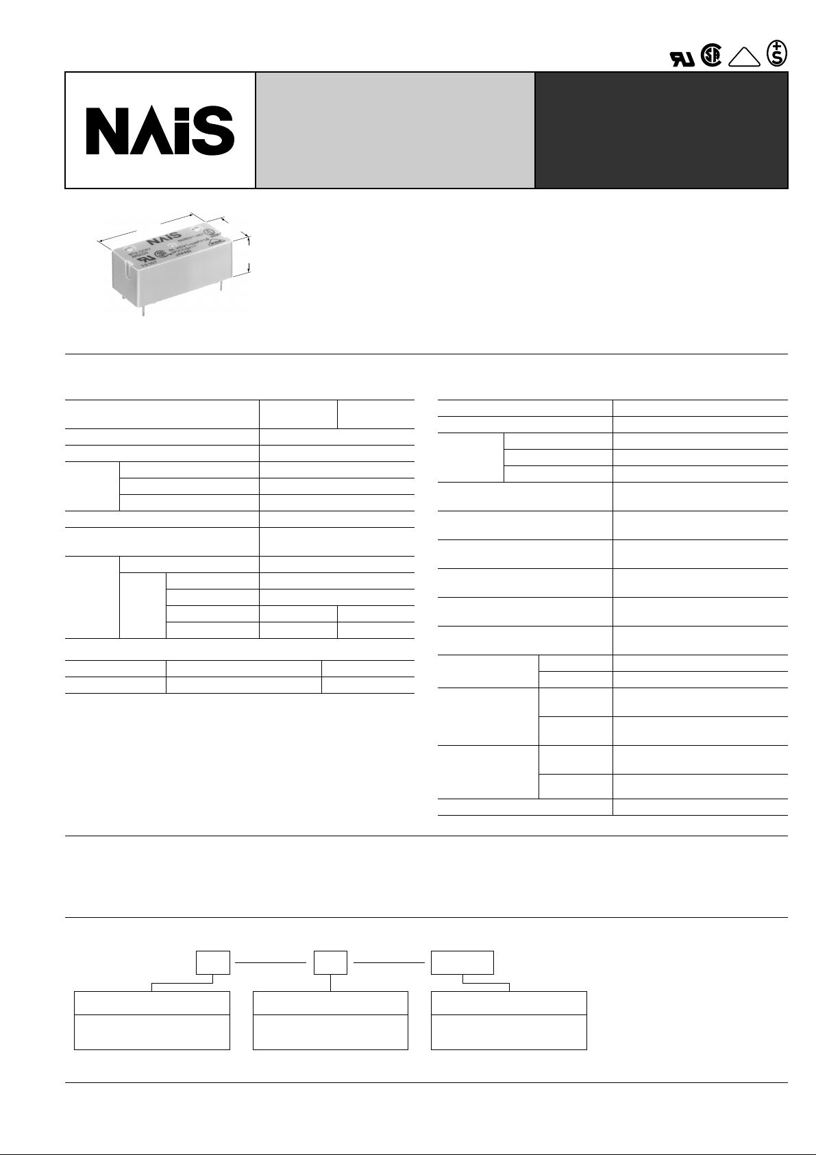
NAIS ST2-L2-DC9V, ST2-L2-DC6V, ST2-L2-DC5V, ST2-L2-DC48V, ST2-L2-DC3V Datasheet
...
VDE
2 ×
3 ×
×
IC DRIVABLE PC BOARD
RELAY FOR FIELD LOAD
ST-RELAYS
SWITCHING
31
1.220
14
.551
11.3
.445
FEATURES
• Sealed to meet the combination process of automatic wave soldering
and cleaning needs
• Latching types available
mm inch
SPECIFICATIONS
Contacts
Arrangement
Contact material Gold flash over silver alloy
Initial contact resistance, max. 30 m Ω
Rating
(resistive)
Max. switching power 2,000 VA, 150 W
Max. switching voltage 380 V AC, 30 V DC
Max. switching current 8 A
HP rating 1/4 HP 125, 250 V AC
Inrush current capability
Mechanical (at 180 cpm) 10
Expected
life (min.
operations)
Electrical
8 A 250 V AC (resistive)
5 A 30 V DC (resistive)
3 A 100 V AC (lamp)
1 A 100 V AC (lamp)
Coil (polarized) (at 25 ° C 77 ° F)
Single side stable Nominal operating power Approx. 240 mW
Latching Nominal set and reset power Approx. 240 mW
Remarks
* Specifications will vary with foreign standards certification ratings.
1
Measurement at same location as "Initial breakdown voltage" section
*
2
*
Detection current: 10 mA
3
Wave is standard shock voltage of ± 1.2 × 50 µ s according to JEC-212-1981
*
4
*
Excluding contact bounce time
5
Half-wave pulse of sine wave: 11ms; detection time: 10 µ s
*
6
*
Half-wave pulse of sine wave: 6ms
7
*
Detection time: 10 µ s
8
Refer to 5. Conditions for operation, transport and storage mentioned in
*
AMBIENT ENVIRONMENT (Page 61).
1 Form A
1 Form B
2 Form A
51 A (TV-3 equivalence) for 1a1b
35 A (TV-1 equivalence) for 2a
7
5
10
5
10
4
10
—3
—
10
4
• High switching capacity and high
sensitivity in subminiature size
150 mW pick-up, 8 A inrush capacity:
51 A for 1a1b, 35 A for 2a
• High shock and vibration resistance
Shock: 20 G, Vibration: 10 to 55 Hz at
double amplitude of 2 mm
Characteristics (at 25 ° C 77 ° F 50% Relative humidity)
Max. operating speed
Initial insulation resistance*
Initial
breakdown
voltage*
Surge voltage between coil and
contact*
Operate time*
Between contact sets
Between open contacts
2
Between contacts and coil
3
4
1
(at nominal voltage)
Release time (without diode)*
4
(at nominal voltage)
Set time*
4
(latching)
(at nominal voltage)
Reset time*
4
(latching)
(at nominal voltage)
Temperature rise
(at 60 ° C)
Shock
resistance
Vibration
resistance
Conditions for operation,
transport and storage*
(Not freezing and condensing at low temperature)
Functional*
Destructive*
Functional*
Destructive
Ambient
8
temp.
Humidity 5 to 85% R.H.
5
6
7
Unit weight Approx. 10g .353 oz
20 cpm (at rated load)
1,000 M Ω (at 500 V DC)
2,000 Vrms
1,200 Vrms
3,750 Vrms
Min. 6,000 V
Max. 15 ms (Approx. 10 ms)
Max. 10 ms (Approx. 8 ms)
Max. 10 ms (Approx. 8 ms)
Max. 10 ms (Approx. 8 ms)
Max. 55 ° C with nominal coil voltage
and at 8 A switching current
Min. 196 m/s
Min. 980 m/s
117.6 m/s
2
{20 G}
2
{100 G}
2
{12 G}, 10 to 55 Hz
at double amplitude of 2 mm
176.4 m/s
2
{18 G}, 10 to 55 Hz
at double amplitude of 3 mm
–40 ° C to +60 ° C
–40 ° Fto +140 ° F
TYPICAL APPLICATIONS
Sequence controllers, facsimiles, telephone controls, remote
control security devices and security equipment.
ORDERING INFORMATION
Ex. ST
Contact arrangement
1: 1 Form A 1 Form B
2: 2 Form A
1 L2 DC48V
Operating function Coil voltage
Nil: Single side stable
L2: 2 coil latching
(Note) Standard packing: Carton; 50 pcs., Case; 500 pcs.
DC 3, 5, 6, 9, 12,
24, 48 V
249
Ω ( ±
Ω ( ±
ST
TYPES AND COIL DATA (at 20 ° C 68 ° F)
Single side stable
1 Form A
1 Form B
Part No.
2 Form A
Nominal
voltage,
V DC
Pick-up voltage,
V DC (max.)
Drop-out
voltage,
V DC (min.)
ST1-DC3V ST2-DC3V 3 2.4 0.3 4.5 38 75
ST1-DC5V ST2-DC5V 5 4.0 0.5 7.5 105 47
ST1-DC6V ST2-DC6V 6 4.8 0.6 9.0 150 40
ST1-DC9V ST2-DC9V 9 7.2 0.9 13.5 360 25
ST1-DC12V ST2-DC12V 12 9.6 1.2 18.0 600 20
ST1-DC24V ST2-DC24V 24 19.2 2.4 36.0 2,400 10
ST1-DC48V ST2-DC48V 48 38.4 4.8 72.0 9,000 4.7
2 coil latching
Part No.
1 Form A
1 Form B
2 Form A
ST1-L2-DC3V ST2-L2-DC3V 3 2.4 4.5 40 75
ST1-L2-DC5V ST2-L2-DC5V 5 4.0 7.5 110 47
ST1-L2-DC6V ST2-L2-DC6V 6 4.8 9.0 155 37.5
ST1-L2-DC9V ST2-L2-DC9V 9 7.2 13.5 360 25
ST1-L2-DC12V ST2-L2-DC12V 12 9.6 18.0 640 18.8
ST1-L2-DC24V ST2-L2-DC24V 24 19.2 36.0 2,400 9.8
ST1-L2-DC48V ST2-L2-DC48V 48 38.4 72.0 10,200 4.7
Nominal
voltage,
V DC
Set and reset
voltage,
V DC (max.)
Maximum allowable voltage,
V DC (60 ° C
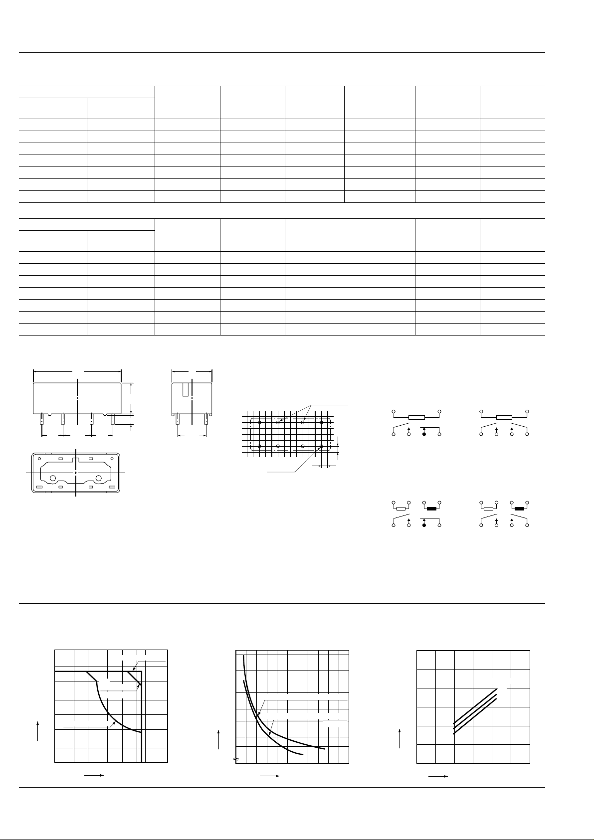
DIMENSIONS
Maximum
allowable voltage,
V DC (60 ° C 140°F)
140°F
)
Coil resistance,
10%)
Coil resistance,
10%)
Nominal
operating
current, mA
Nominal
operating
current, mA
mm inch
31.0
1.220
11.0
.433
0.3
.012
3.5 .138
7.62
.300
85
10.16
.400
76
7.62
.300
4321
General tolerance: ± 0.2 ± .008
14
.551
10.16
.400
PC board pattern
(Copper-side view)
2 coil latching
types only.
8-DIA. 1.4
.055
Tolerance: ± 0.1 ± .004
2.54
.100
2.54
.100
Schematic (Bottom view)
Single side stable
1a1b 2a
14
–+
5678
(Deenergized condition)
2 coil latching
1a1b
12
–+
34
+–
5678
(Reset condition)
Diagram shows the "reset" position when terminals 3 and 4
are energized. Energize terminals 1 and 2 to transfer contacts.
REFERENCE DATA
1. Max. switching power 2. Life curve 3. Coil temperature rise
1,000
500
200
100
50
Life, 10 k operations
20
10
AC 250 V, 125 V resistive load
AC 250 V, 125 V inductive load
12345678910
Current, A
(Pf = 0.4)
10
5
2
1
Current, A
0.5
0.2
0.1
AC resistive load
AC
inductive load
(cosϕ =0.4)
DC resistive load
10 20 50 100 200 300
Voltage, V
Sample: ST1-DC24V
60
50
40
30
Temperature rise, °C
20
10
0
0.1 0.2 0.3 0.4 0.5
Coil operating power, W
14
–+
5678
2a
12–+34
Diagram shows the "reset" position when terminals 3 and 4
are energized. Energize terminals 1 and 2 to transfer contacts.
Contact current
8 A
5 A
0 A
+–
5678
250
 Loading...