

21±0.2
.827±.008
12 3 4
–+
3.5±0.2
.138±.008
12.5±0.2
.492±.008
mm inch
POWER PhotoMOS RELAYS
with Internal Varistor
FEATURES
1. P ower PhotoMOS rela y with internal
varistor
An internal varistor on the output side protects the output MOSFET from the reverse voltage from an external voltage
surge or inductive load.
2. High capacity PhotoMOS relay
Supports control of minute loads to a
maximum 3.0 A. Suitable for output control.
3. Supports both AC and DC
Bi-directional control so there is no need
to differentiate according to the load as in
conventional SSR's.
4. Can be placed on-board the 4-unit
relay (power photoMOS relay type)
PhotoMOS
RELAYS
5. Ideal for inductive loads
Ideal for inductive loads such as motors,
solenoids, and electro-magnetic contactors.
6. High sensitivity, low ON resistance
Can control a maximum 3.0 A load with a
5 mA input current. Lo w On resistance of
0.18 Ω (AQZ202V).
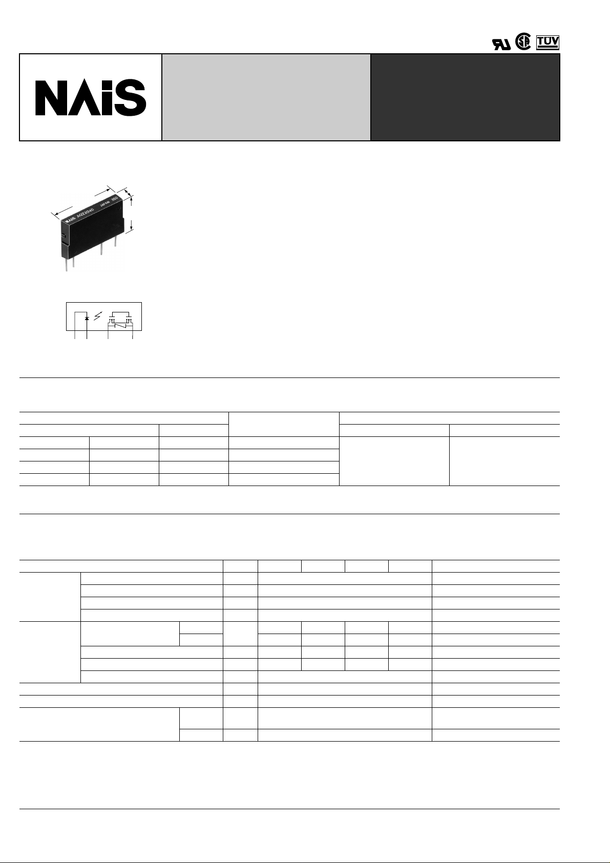
7. Compact slim-type 4-pin SIL
(W) 3.5 × (L) 21.0 × (H) 12.5 mm (W)
.138 × (L) .827 × (H) .492 inch . The com-
pact 73.5mm
age allows high density mounting.
8. Sockets also available
9. Promoting the CE making
(Please inquire for further details.)
2
size of the 4-pin SIL pack-
TYPES
AC/DC type
Output rating
Load voltage (Effective Vrms) Load current Inner carton Outer carton
17 V AC 22 V DC 3.0 A AQZ202V
30 V AC 38 V DC 2.0 A AQZ205V
60 V AC 85 V DC 1.0 A AQZ207V
140 V AC 180 V DC 0.5 A AQZ204V
Note: Refer to the recommended load voltage.
Part No.
25 pcs. 500 pcs.
Packing quantity
RATING
AC/DC type
1) Absolute maximum ratings (Ambient temperature: 25 ° C 77 ° F)
Item Symbol AQZ202V AQZ205V AQZ207V AQZ204V Remarks
LED forward current I
Input
Output
Total power dissipation P
I/O isolation voltage V
Temperature limits
LED reverse voltage V
Peak forward current I
Power dissipation P
Load voltage
Continuous load current (Peak AC) I
Peak load current I
Power dissipation P
AC
DC 22 V 38 V 85 V 180 V
Operating T
Storage T
FP
V
peak
F
R
in
17 V 30 V 60 V 140 V Effective Vrms
L
3.0 A 2.0 A 1.0 A 0.5 A
L
9.0 A 6.0 A 3.0 A 1.5 A 100 ms (1 shot), V
out
T
iso
opr
stg
–40 ° C to +85 ° C –40 ° F to +185 ° F
–40 ° C to +100 ° C –40 ° F to +212 ° F
50 mA
3 V
1 A f = 100 Hz, Duty factor = 0.1%
75 mW
1.6 W
1.6 W
2,500 V AC
Non-condensing at low
temperatures
= DC
L
210
0.5
0.4
0.3
0.2
0.1
0
0-40 -20
20
40 60 8085
Ambient temperature, °C
On resistance, Ω
AQZ205V
AQZ202V
■
■
■
AQZ20 ❍ V
2) Electrical characteristics (Ambient temperature: 25 ° C 77 ° F)
Item Symbol AQZ202V AQZ205V AQZ207V AQZ204V Remarks
Typical
Maximum 3.0 mA
Minimum
Typical 0.9 mA
Typical
Maximum 1.5 V
Typical
Maximum 0.18 Ω 0.34 Ω
Typical
Maximum 5.0 ms
Typical 5.64 ms 5.65 ms 2.57 ms 3.88 ms
I
Fon
Foff
I
V
R
Leak
F
on
1.16 V (1.25 V at I
0.11 Ω 0.23 Ω
2.46 ms 2.40 ms 1.12 ms 1.65 ms
T
on
Maximum 10.0 ms
Typical
Maximum 3.0 ms
Typical
Maximum 1.5 pF
Minimum R
0.22 ms 0.21 ms 0.10 ms 0.08 ms
T
off
C
iso
iso
Maximum — 1.0 cps
Input
Output
Transfer
characteristics
LED operate current
LED turn off current
LED dropout voltage
On resistance
Off state leakage current Maximum I
Turn on time*
Switching
speed
Turn off time*
I/O capacitance
Initial I/O isolation
resistance
Maximum operating
frequency
Vibration resistance Minimum — 10 to 55 Hz at double amplitude of 3 mm 2 hours for 3 axes
Shock resistance Minimum — 4,900 m/s
3) Internal varistor characteristics
Item AQZ202V AQZ205V AQZ207V AQZ204V
Varistor voltage 27 V 47 V 100 V 220 V
Maximum energy 0.5 J 1.0 J 2.0 J 4.5 J
Note: When using the relay to absorb the reverse voltage during inductive load switching, make sure the load is within the inductance range given in the internal varistor
characteristics data below, rather than the energy resistance range for the internal varistor. Note, the inductance range will differ if the switching frequency is higher
than the rate given for the characteristics data conditions.
Note: Recommendable LED forward current I
*Turn on/off time
= 5 to 10 mA. For type of connection, see page 35.
F
1.0 mA
0.4 mA
1 mA
0.8 pF
1,000 M Ω
F
= 50 mA)
0.7 Ω
1.1 Ω
2.1 Ω
3.2 Ω
L
I
= 100 mA
L
V
= 10 V
L
I
= 100 mA
L
V
= 10 V
F
I
= 10 mA
F
I
= 10 mA
L
I
= Max.
Within 1 s on time
F
I
= 0
= Max. DC
L
V
I
F
= 10 mA
= 100 mA
L
I
V
= 10 V
L
I
F
= 5 mA
= 100 mA
L
I
V
= 10 V
L
I
F
= 5 mA or 10 mA
= 100 mA
L
I
V
= 10 V
L
f = 1 MHz
V
= 0
B
500 V DC
I
= 10 mA
F
Duty factor = 50%
I
= Max., V
L
2
{500 G}1 ms 3 times for 3 axes
= Max.
L
Input
Output 10%
Ton
Toff
90%
For Dimensions, see Page 29.
For Schematic and Wiring Diagrams, see Page 35.
For Cautions for Use, see Page 40.
REFERENCE DATA
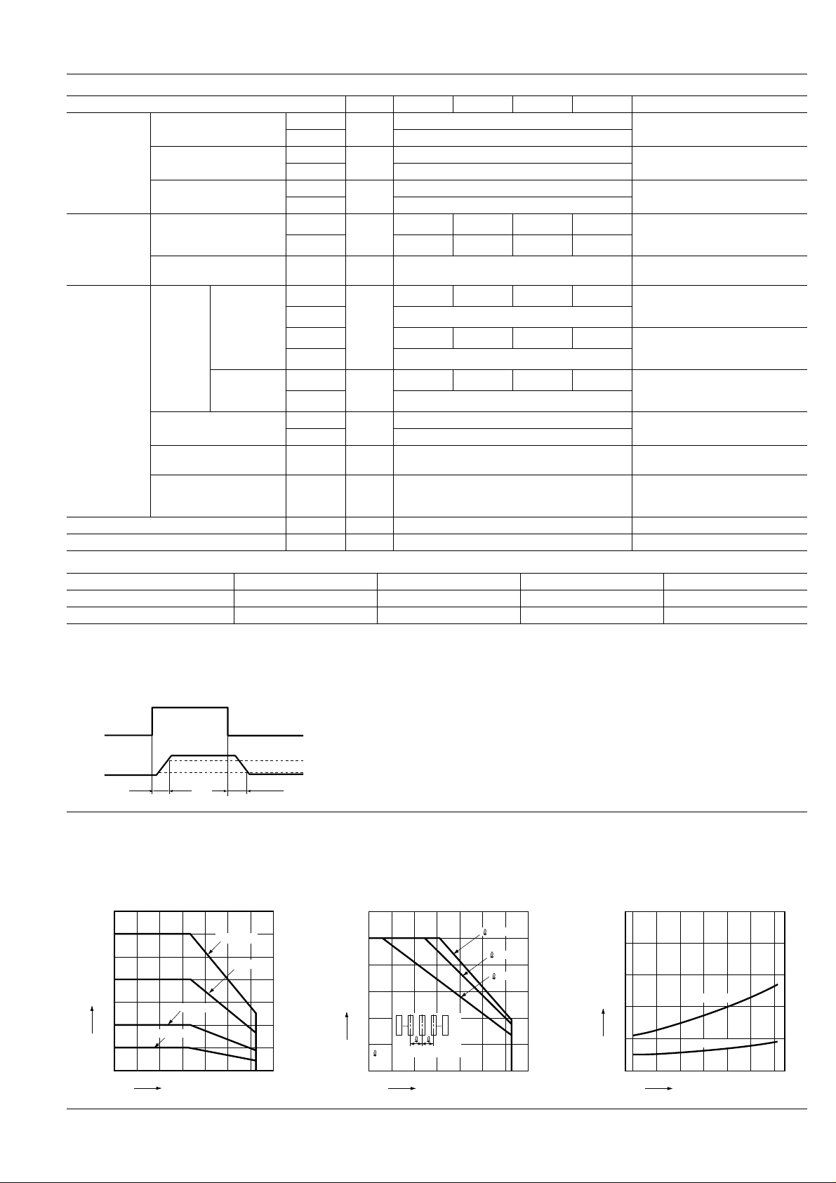
1. Load current vs. ambient temperature characteristics
Allowable ambient temperature: –40°C to +85°C
3.5
3.0
2.5
2.0
Load current, A
1.5
1.0
0.5
0
AQZ204V
0-40 -20 20 40 60 8085 100
Ambient temperature, °C
–40°F to +185°F
AQZ202V
AQZ205V
AQZ207V
2. Load current vs. ambient temperature characteristics in adjacent mounting
L
I
: Load current;
(max.): Maximum continuous load current
L
I
120
100
80
60
(max.)×100,%
L
/I
L
I
40
20
= Adjacent mounting pitch
0
0-20-40 20 40 60 100
Ambient temperature, °C
= 20mm
= 10mm
= 5mm
8085
3.-(1) On resistance vs. ambient temperature
characteristics
LED current: 10 mA;
Continuous load current: 3.0 A (DC) (AQZ202V),
2.0 A (DC) (AQZ205V),
211
 Loading...