

NAIS AQY414SZ, AQY414SX, AQY410SZ, AQY410SX Datasheet
-
-
S
×
×
TESTING
GU (General Use) Type
SOP Series
PhotoMOS
1- Channel (Form B)
4-Pin T ype
RELAYS
4.3±0.2
.169±.008
1
2
4.4±0.2
.173±.008
2.1±0.2
.083±.008
mm inch
4
3
FEATURES
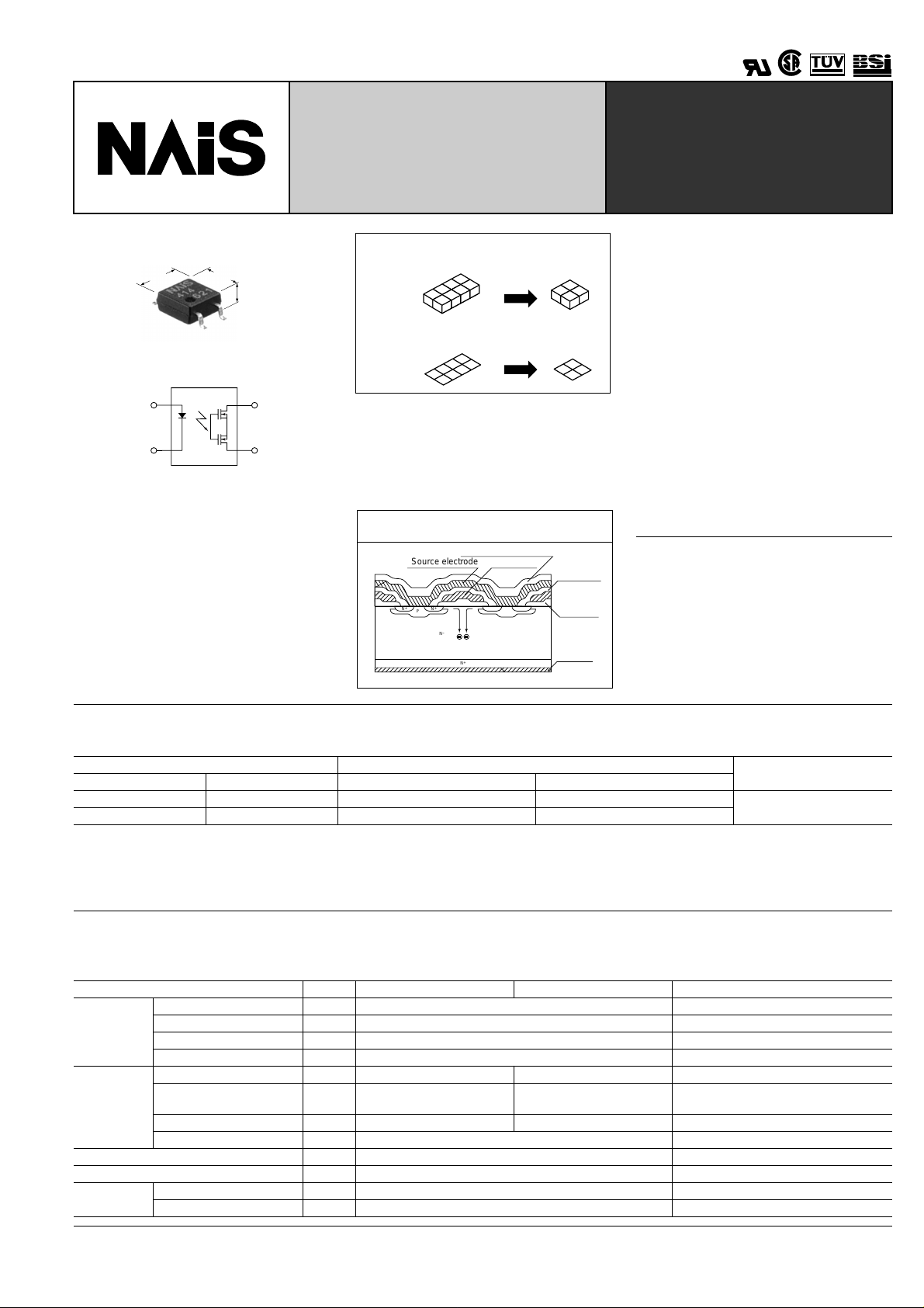
1. SO package 4-Pin type in super miniature design
The device comes in a super-miniature
SO package 4-Pin type measuring (W)
4.3
(L) 4.4 × (H) 2.1 mm (W) .169 × (L)
.173
(H) .083 inch —approx. 70% of the
volume and 70% of the footprint size of SO
package 6-pin type PhotoMOS Relays.
(4-pin)(6-pin)
Approx. 70%
Volume
Approx. 70%
Footprint
2. Low on resistance for normallyclosed type
This has been realized thanks to the builtin MOSFET processed by our proprietary
method, DSD (Double-diffused and Selective Doping) method.
Cross section of the normally-closed type of
power MOS
Source electrode
N+N
+
+
P
–
N
Passivation membrane
Gate electrode
+
N+N
+
P
+
N
Intermediate
insulating
membrane
Gate
oxidation
membrane
Drain
electrode
3. Tape and reel
The device comes standard in a tape and
reel (1,000 pcs./reel) to facilitate automatic
insertion machines.
4. Controls low-level analog signals
PhotoMOS relays feature extremely low
closed-circuit offset voltage to enable con
trol of low-level analog signals without dis
tortion.
5. Low-level off state leakage current
In contrast to the SSR with an off state
leakage current of several milliamps, the
PhotoMOS relay features a very small off
state leakage current of 1nA even with the
rated load voltage of 350 V (AQY410S).
TYPICAL APPLICATION
• Telecommunications (PC, Electoronic
Notepad)
• Measuring and Testing equipment
• Factory Automation Equipment
• Security equipment
• High speed inspection machines
TYPES
AC/DC type
Output rating* Part No.
Load voltage Load current Picked from the 1/2-pin side Picked from the 3/4-pin side
350 V 120 mA AQY410SX AQY410SZ
400 V 100 mA AQY414SX AQY414SZ
* Indicate the peak AC and DC values.
Notes: (1) Tape package is the standard packing style. Also available in tube. (Part No. suffix "X" or "Z" is not needed when ordering; Tube: 100 pcs.;
Case: 2,000 pcs.)
(2) For space reasons, the top two letters of the product number "A QY" and "S" are omitted on the product seal. The package type indicator "X"
and "Z" are omitted from the seal. (Ex. the label for product number AQY414S is 414).
Packing quantity in tape
and reel
1,000 pcs.
RATING
AC/DC type
1. Absolute maximum ratings (Ambient temperature: 25 ° C 77 ° F)
Item Symbol AQY410S AQY414S Remarks
LED forward current I
Input
Output
Total power dissipation P
I/O isolation voltage V
T emperture
limits
LED reverse voltage V
Peak forward current I
Power dissipation P
Load voltage (peak AC) V
Continuous load current
(peak AC)
Peak load current I
Power dissipation P
Operating T
Storage T
FP
I
peak
F
R
in
L
L
out
T
iso
opr
stg
350 V 400 V
0.12 A 0.1 A
0.3 A 0.24 A 100ms (1 shot), V
–40 ° C to +85 ° C –40 ° F to +185 ° F Non-condensing at low temperatures
–40 ° C to +100 ° C –40 ° F to +212 ° F
50 mA
3 V
1 A f = 100 Hz, Duty factor = 0.1%
75 mW
L
= DC
300 mW
350 mW
1,500 V AC
63
AQY41 ❍ S
2. Electrical characteristics (Ambient temperature: 25 ° C 77 ° F )
Item Symbol AQY410S AQY414S Remarks
LED operate
(OFF) current
Input
LED reverse
(ON) current
LED dropout
voltage
On resistance
Output
Off state leakage current
Operate (OFF)
time*
Reverse (ON)
Transfer
time*
characteristics
I/O capacitance
Initial I/O isola-
tion resistance
Note: Recommendable LED forward current I
Typical
Maximum 3 mA
Minimum
Typical 0.85 mA
Typical
Maximum 1.5 V
Typical
Maximum 25 Ω
Maximum I
Typical
Maximum 1 ms
Typical
Maximum 1 ms
Typical
Maximum 1.5 pF
Minimum R
Fon
I
Foff
I
F
V
on
R
Leak
T
on
T
off
C
iso
iso
= 5mA. For type of connection, see page 32.
F
1 µ
0.9 mA
0.4 mA
1.14 V (1.25 V at I
F
= 50 mA)
18 Ω
A
0.52 ms 0.47 ms
0.23 ms 0.28 ms
0.8 pF
1,000 M Ω
*Operate/Reverse time
26 Ω
35 Ω
■
■
■
L
I
= Max.
L
I
= Max.
F
I
= 5 mA
F
I
= 0 mA
L
I
= Max.
Within 1 s on time
F
I
= 5 mA
= Max.
L
V
I
= 0 mA-->5 mA
F
I
= Max.
L
I
= 5 mA-->0 mA
F
I
= Max.
L
f = 1 MHz
V
= 0
B
500 V DC
For Dimensions, see Page 28.
For Schematic and Wiring Diagrams, see Page 32.
For Cautions for Use, see Page 36.
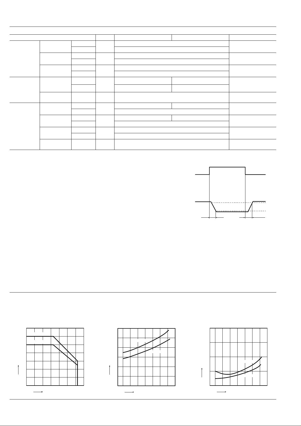
REFERENCE DATA
1. Load current vs. ambient temperature characteristics
Allowable ambient temperature:
–40 ° C to +85 ° C
–40 ° F to +185 ° F
140
AQY410S
120
AQY414S
100
80
60
Load current, mA
40
20
0
–40 100
0–20 20 40 60
Ambient temperature, °C
8085
2. On resistance vs. ambient temperature characteristics
Measured portion: between terminals 3 and 4;
LED current: 0 mA;
Continuous load current: Max.(DC)
30
25
20
15
On resistance, Ω
10
5
0
AQY414S
–40 –20
Ambient temperature, °C
AQY410S
0204060
8085
100
Input
Output
Toff
3. Operate (OFF) time vs . ambient temper ature
characteristics
LED current: 5 mA; Load voltage: Max.(DC);
Continuous load current: Max.(DC)
2
1.5
1
Operate (OFF) time, ms
0.5
0
AQY414S
AQY410S
0–40 –20 20 40 60
Ambient temperature, °C
Ton
80 85
10%
90%
100
64
 Loading...