

NAIS AQV227NSZ, AQV225NSZ, AQV225NSX, AQV224NSZ, AQV224NSX Datasheet
×
RF (Radio Frequency) Type
SOP Series
PhotoMOS
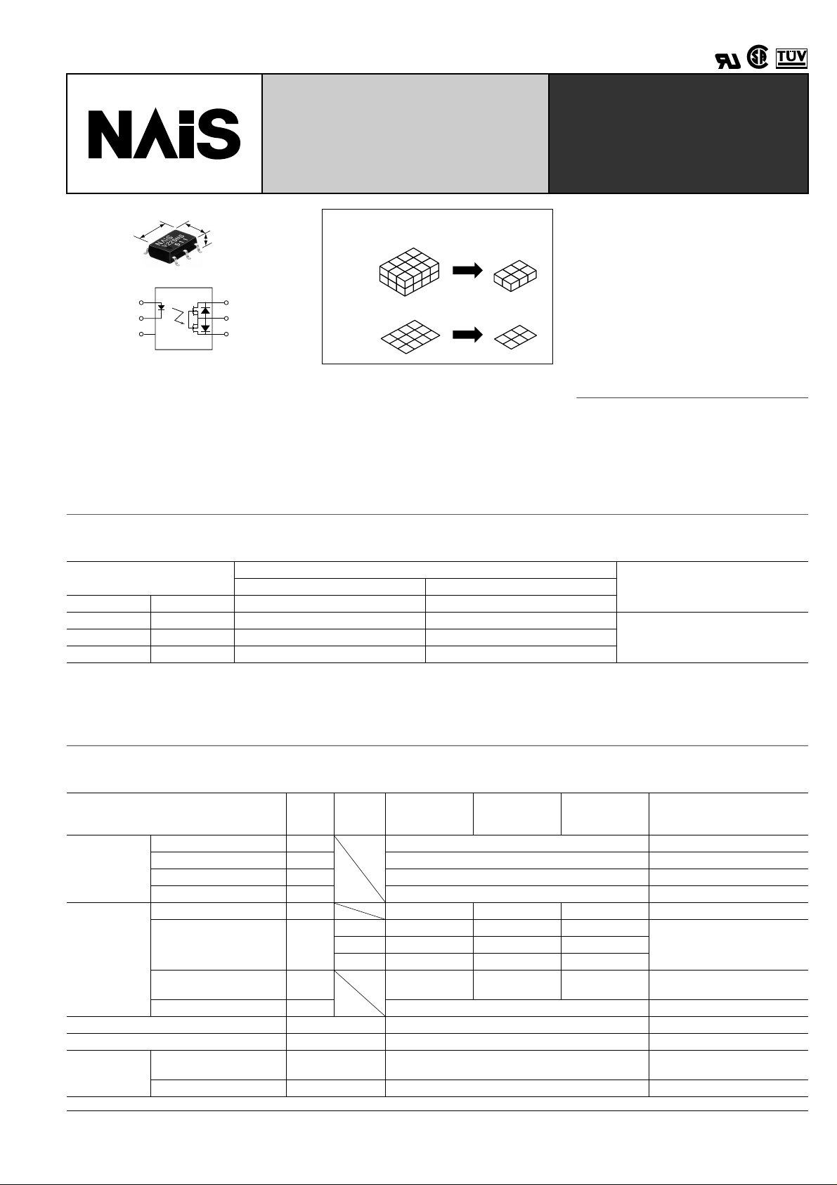
[1-Channel (Form A) Type]
—Low On resistance—
RELAYS
6.3±0.2
.248±.008
1
2
3
4.4±0.2
.173±.008
2.1±0.2
.083±.008
mm inch
6
5
4
(SOP)(DIP)
Approx. 25%
Volume
Approx. 50%
Footprint
toMOS relay has only 30 pA ev en with the
rated load voltage of 80 V (AQV225NS).
4. Controls low-level analog signals
PhotoMOS relays feature extremely low
closed-circuit offset voltage to enable
control of low-level analog signals without
distortion.
5. Tape and reel
The device comes standard in a tape and
reel (1,000 pcs./reel) to facilitate automat-
FEATURES
1. 1-channel (Form A) in super miniature design
The device comes in a super-miniature
SO package measuring (W) 4.4 × (L) 6.3
(H) 2.1 mm (W).173 × (L) .248 × (H) .083
inch —approx. 25% of the volume and
50% of the footprint size of DIP type PhotoMOS Relays.
2. Low capacitance between output
terminals ensure high response
speed:
The capacitance between output terminals is small, typically 10 pF. This enables
for a fast operation speed of 200 µ s.
3. Low-level off state leakage current:
The SSR has an off state leakage current
of several milliamperes , whereas the Pho-
ic insertion machines.
TYPICAL APPLICATIONS
• T elephones
• Measuring instruments
• Computer
• Industrial robots
• High-speed inspection machines
TYPES
1. AC/DC type
Output rating*
Load voltage Load current 1 Form A 1 Form A
80 V 120 mA AQV225NSX AQV225NSZ
400 V 40 mA AQV224NSX AQV224NSZ
*Indicate the peak AC and DC values.
Notes: (1) Tape package is the standard packing style. Also available in tube. (Part No. suffix "X" or "Z" is not needed when ordering; Tube: 75 pcs.;
Case: 1,500 pcs.)
(2) For space reasons, the top two letters of the product number "AQ" are omitted on the product seal. The package type indicator "X" and "Z"
are also omitted from the seal. (Ex. the label for product number AQV224NS is V224NS).
Part No.
Packing quantity in tape and reelPicked from the 1/2/3-pin side Picked from the 4/5/6-pin side
1,000 pcs.200 V 50 mA AQV227NSX AQV227NSZ
RATING
1. Absolute maximum ratings (Ambient temperature: 25 ° C 77 ° F)
FP
peak
Type of
connec-
tion
F
R
in
L
A 0.12 A 0.05 A 0.04 A
L
out
T
iso
opr
stg
B 0.15 A 0.06 A 0.05 A
C 0.25 A 0.08 A 0.06 A
AQV225NS AQV227NS AQV224NS Remarks
Item Symbol
LED forward current I
Input
Output
Total power dissipation P
I/O isolation voltage V
T emperature
limits
LED reverse voltage V
Peak forward current I
Power dissipation P
Load voltage (peak AC) V
Continuous load current I
Peak load current I
Power dissipation P
Operating T
Storage T
50 mA
3 V
1 A f = 100 Hz, Duty factor = 0.1%
75 mW
80 V 200 V 400 V
0.36 A 0.15 A 0.12 A
450 mW
500 mW
1,500 V AC
–40 ° C to +85 ° C –40 ° F to +185 ° F
–40 ° C to +100 ° C –40 ° F to +212 ° F
A connection: Peak AC, DC
B, C connection: DC
A connection: 100 ms (1 shot),
L
V
= DC
Non-condensing at low
temperatures
149
AQV22 ❍ NS
2. Electrical characteristics (Ambient temperature: 25 ° C 77 ° F)
LED operate current
Input
LED turn off current
LED dropout voltage
On resistance
Output
Output capacitance
Off state leakage current
Turn on time*
Transfer
Turn off time*
characteristics
I/O capacitance
Initial I/O isolation
resistance
*Turn on/Turn off time
Item Symbol
Typical
Maximum 3 mA
Minimum
Typical 0.65 mA
Typical
Maximum 1.5 V
Typical
Maximum 10.0 Ω
Typical
Maximum 5.0 Ω
Typical
Maximum 2.5 Ω
Typical
Maximum 15 pF
Typical
Maximum 10 nA
Typical
Maximum 0.5 ms
Typical
Maximum 0.2 ms
Typical
Maximum 1.5 pF
Minimum R
= 5 mA.
F
connec-
I
Fon
Foff
I
F
V
on
R
R
on
R
on
C
out
I
leak
T
on
T
off
C
iso
iso
Type of
AQV225NS AQV227NS AQV224NS Remarks
tion
—
—
—
A
B
C
1.14 V (1.25 V at I
7.0 Ω
3.5 Ω
1.8 Ω
0.7 mA
0.4 mA
30 Ω
50 Ω
16 Ω
25 Ω
12.5 Ω
10 pF
—
—
—
—
30 pA 30 pA 90 pA
0.25 ms
0.08 ms
0.8 pF
— 1,000 M Ω
8 Ω
F
= 50 mA)
For type of connection, see Page 31.Note: Recommendable LED forward current I
■
■
■
L
I
= Max.
L
I
= Max.
F
I
= 5 mA
F
I
70 Ω
100 Ω
55 Ω
70 Ω
28 Ω
35 Ω
= 5 mA
= Max.
L
I
Within 1 s on time
F
I
= 5 mA
= Max.
L
I
Within 1 s on time
F
I
= 5 mA
= Max.
L
I
Within 1 s on time
I
F
= 0
= 0
B
V
f = 1 MHz
I
= 0
F
V
= Max.
L
I
= 5 mA
F
I
= Max.
L
I
= 5 mA
F
I
= Max.
L
f = 1 MHz
V
= 0
B
500 V DC
Input
Output 10%
Ton
Toff
REFERENCE DATA
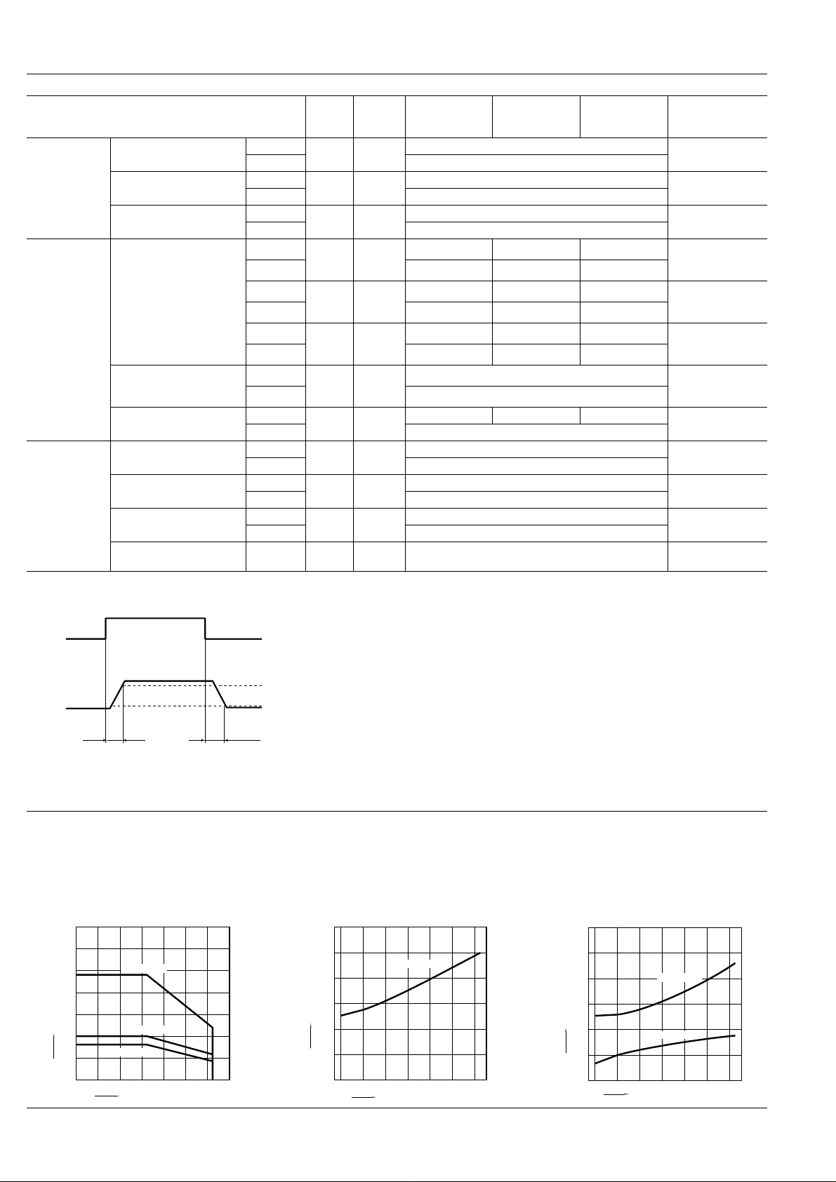
1. Load current vs. ambient temperature characteristics
Allowable ambient temperature: –40 ° C to +85 ° C
Type of connection: A
150
AQV225NS
100
Load current, mA
50
AQV227NS
AQV224NS
–40 ° F to +185 ° F
90%
For Dimensions, see Page 28.
For Schematic and Wiring Diagrams, see Page 31.
For Cautions for Use, see Page 36.
2.-(1) On resistance vs. ambient temperature
characteristics
Measured portion: between terminals 4 and 6;
LED current: 5 mA;
Load voltage: Max. (DC);
Continuous load current: Max. (DC)
12.0
10.0
On resistance, Ω
8.0
6.0
4.0
2.0
AQV225NS
2.-(2) On resistance vs. ambient temperature
characteristics
Measured portion: between terminals 4 and 6;
LED current: 5 mA;
Load voltage: Max. (DC);
Continuous load current: Max. (DC)
120
100
80
60
On resistance, Ω
40
20
AQV224NS
AQV227NS
150
0
0204060–20
Ambient temperature, °C
8085
100–40
0
–40
0–20 20 40 60
Ambient temperature, °C
80 85
0
–40
0–20 20 40 60
Ambient temperature, °C
8085
 Loading...