

NAIS AQV221NAZ, AQV221NAX, AQV221NA, AQV221N Datasheet
BSI
pending
8.8±0.05
.346±.002
1
2
3
6.4±0.05
.252±.002
3.6±0.2
.142±.008
8.8±0.05
.346±.002
6.4±0.05
.252±.002
6
5
4
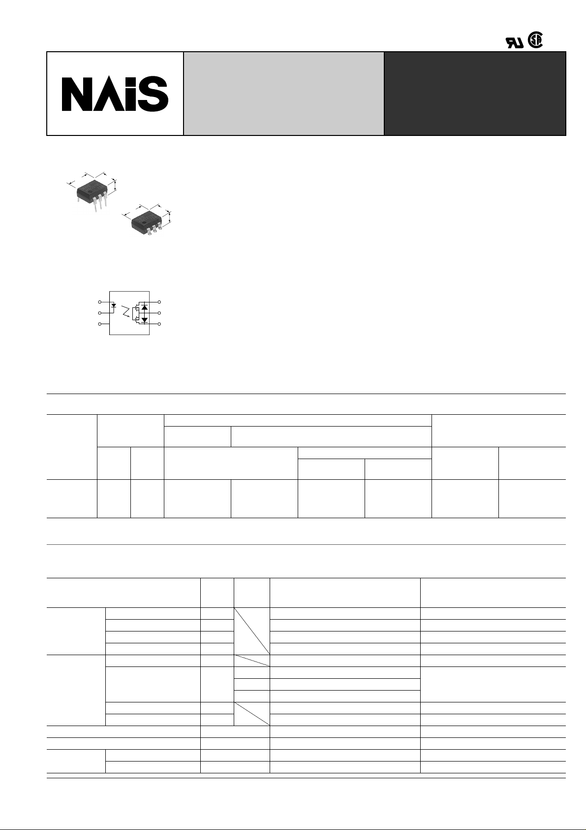
RF (Radio Frequency) Type
Low C and R
FEATURES
1. Low output capacitance between
output terminals and low ON-resistance
2. High speed switching (Turn on time:
3.9±0.2
.154±.008
mm inch
typ. 200 µ s)
3. High sensitivity
Control loads up to 250mA with input current 5mA
4. Low-level off state leakage current
The SSR has an off state leakage current
of several milliamperes, where as this
PhotoMOS relay has only 20pA (typical)
even with the rated load voltage
5. Controls low-level analog signals
PhotoMOS relays features e xtremely lo wclosed-circuit offset voltage to enable
control of low-level analog signals without
distortion
6. Low thermal electromotive force
(Approx. 1 µ V)
PhotoMOS
RELAYS
TYPICAL APPLICATIONS
Measuring and testing equipment
1. Testing equipment for semiconductor
performance
IC tester, Liquid crystal driver tester,
semiconductor performance tester
2. Board tester
Bear board tester, In-circuit tester,
function tester
3. Medical equipment
Ultrasonic wave diagnostic machine
4. Multi-point recorder
(warping, thermo couple)
TYPES
Part No.
Output rating*
Type
Load
voltage
AC/DC type 40 V 150 mA AQV221N AQV221NA AQV221NAX AQV221NAZ
*Indicate the peak AC and DC values.
Note: For space reasons, the package type indicator "X" and "Z" are omitted from the seal.
Load
current
Through hole
terminal
Tube packing style
Surface-mount terminal
Tape and reel packing style
Picked from the
1/2/3-pin side
Picked from the
4/5/6-pin side
RATING
1. Absolute maximum ratings (Ambient temperature: 25 ° C 77 ° F)
FP
peak
Type of
connec-
tion
F
R
in
L
A 0.15 A
L
out
T
iso
opr
stg
B 0.18 A
C 0.25 A
–40 ° C to +85 ° C –40 ° F to +185 ° F Non-condensing at low temperatures
–40 ° C to +100 ° C –40 ° F to +212 ° F
AQV221N(A) Remarks
50 mA
3 V
1 A f = 100 Hz, Duty factor = 0.1%
75 mW
40 V
0.45 A A connection: 100 ms (1 shot), V
360 mW
410 mW
1,500 V AC
Item Symbol
LED forward current I
Input
Output
Total power dissipation P
I/O isolation voltage V
T emperature
limits
LED reverse voltage V
Peak forward current I
Power dissipation P
Load voltage (peak AC) V
Continuous load current I
Peak load current I
Power dissipation P
Operating T
Storage T
Packing quantity
Tube Tape and reel
1 tube contains
50 pcs.
1 batch contains
500 pcs.
A connection: Peak AC, DC
B, C connection: DC
1,000 pcs.
L
= DC
145
AQV221N
2. Electrical characteristics (Ambient temperature: 25 ° C 77 ° F)
Item Symbol
LED operate current
Input
LED turn off current
LED dropout voltage
On resistance #
Output
Output capacitance #
Off state leakage current
Switching
speed
Transfer
characteristics
I/O capacitance
Initial I/O isolation resistance Minimum R
*Turn on/Turn off time
Turn on time*
Turn off time*
Typical
Maximum 3.0 mA
Minimum
Typical 0.85 mA
Typical
Maximum 1.5 V
Typical
Maximum 15 Ω
Typical
Maximum 7.5 Ω
Typical
Maximum 3.8 Ω
Typical
Maximum 5 pF
Typical
Maximum 10 nA
Typical
Maximum 0.5 ms
Typical
Maximum 0.2 ms
Typical
Maximum 1.5 pF
= 5mA
F
I
Fon
Foff
I
F
V
on
R
R
on
R
on
C
out
I
Leak
T
on
T
off
C
iso
iso
Type of
connec-
tion**
—
—
—
1.14 V (1.25 V at I
A
B
C
A
—
—
—
—
— 1,000 M Ω
■
■
■
AQV221N(A) Remarks
0.90 mA
0.4 mA
9.8 Ω
F
= 50 mA)
I
I
I
I
I
Within 1 s on time
5 Ω
I
I
Within 1 s on time
2.5 Ω
I
I
Within 1 s on time
3.9 pF
I
V
f = 1 MHz
20 pA
I
V
0.2 ms
I
I
0.08 ms
I
I
0.8 pF
f = 1 MHz
V
500 V DC
**For type of connection, see Page 31.Note: Recommendable LED forward current I
L
= Max.
L
= Max.
F
= 5 mA
F
= 0 mA
= Max.
L
F
= 5 mA
= Max.
L
F
= 5 mA
= Max.
L
F
= 0
= 0V
B
= 0
F
= Max.
L
= 5 mA
F
= Max.
L
= 5 mA
F
= Max.
L
= 0
B
Input
Output 10%
Ton
Toff
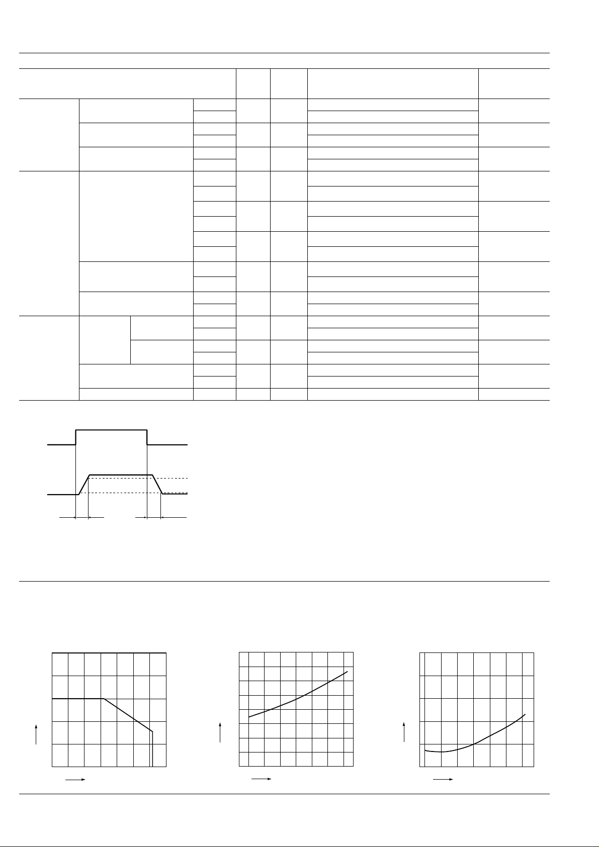
REFERENCE DATA
1. Load current vs. ambient temperature characteristics
Allowable ambient temperature: –40 ° C to +85 ° C
Type of connection: A
250
200
150
Load current, mA
100
50
0
0-40 -20 20 40 60
Ambient temperature, °C
–40 ° F to +185 ° F
8085
100
90%
binations carried in this catalog are also available.
(There is a trade-off between R
For more information, please contact our sales office in your area.
For Dimensions, see Page 27.
For Schematic and Wiring Diagrams, see Page 31.
For Cautions for Use, see Page 36.
2. On resistance vs. ambient temperature characteristics
Measured portion: between terminals 4 and 6;
LED current: 5 mA; Load voltage: Max. (DC);
Continuous load current: Max. (DC)
16.0
14.0
12.0
10.0
8.0
On resistance, Ω
6.0
4.0
2.0
# Other types of products than the C
0
0-40 -20 20 40 60
Ambient temperature, °C
(typ. 3.9pF) and R
out
and C
on
8085
(A connection typ. 9.8 Ω ) com-
on
both cannot be reduced at the same time.)
out
3. Turn on time vs. ambient temperature characteristics
LED current: 5 mA;
Load voltage: Max. (DC);
Continuous load current: Max. (DC)
1.0
0.8
0.6
Turn on time, ms
0.4
0.2
0
0-40 -20 20 40 60
Ambient temperature, °C
8085
146
 Loading...