

NAIS AQS610TSZ, AQS610TSX Datasheet
AQS610TS
93
2
3
4
5
6
7
16
15
14
13
1
8
12
11
10
9
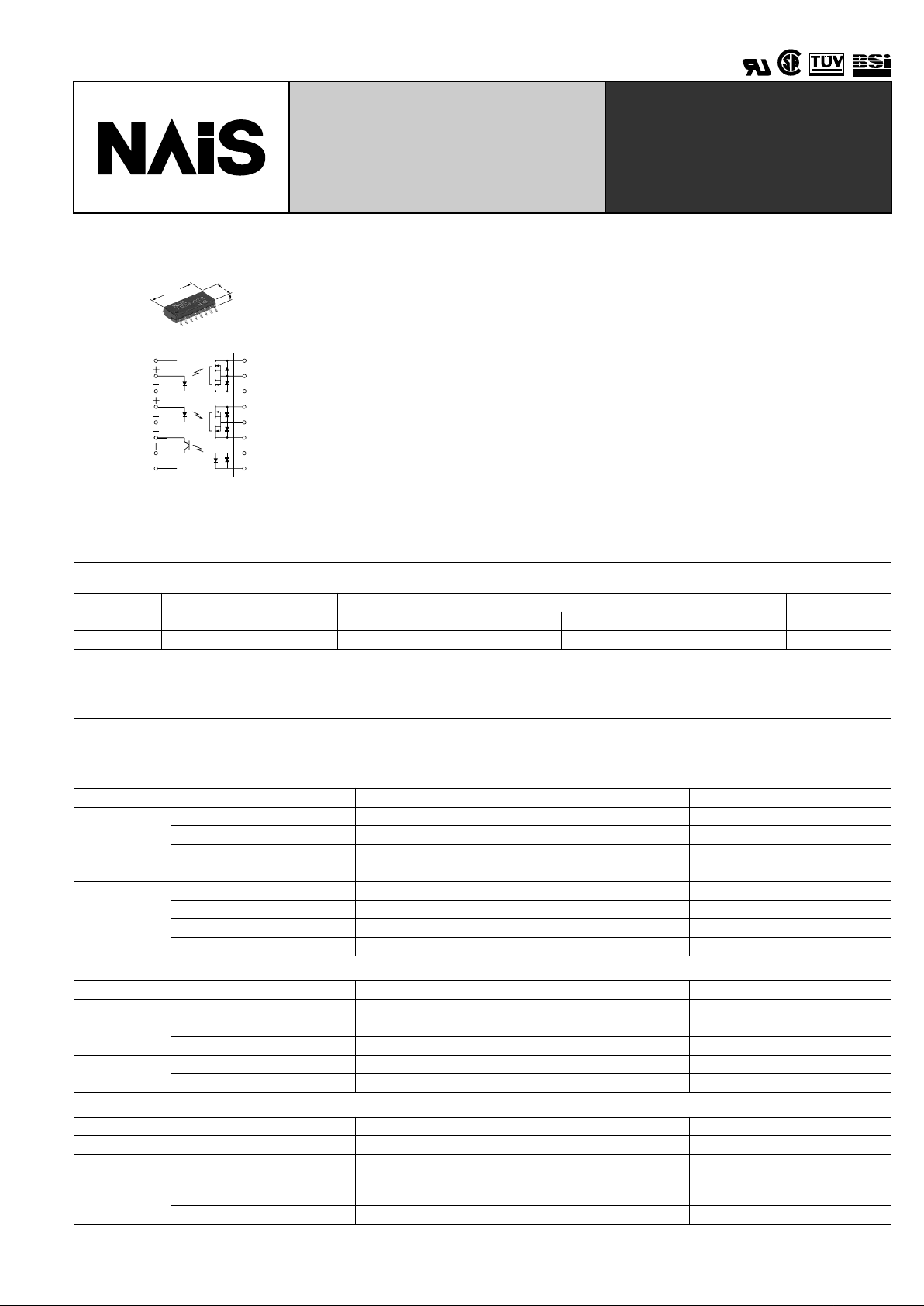
Relay portion
(2,3,14,15,16 pins)
(4,5,11,12,13 pins)
Detector portion
(6,7,9,10 pins)
PhotoMOS
RELAYS
GU (General Use) Type
SOP Series
Multi-function (1a1b MOSFET
& optocoupler) 16 Pin Type
1a1b MOSFET Relay and
1 optocoupler type
mm inch
2.1
.083
4.4
.173
10.37
.408
FEATURES
1. SO package 16-Pin type in super
miniature design
The device comes in a super-miniature
SO package 16-Pin type measuring
(W)4.4 × (L)10.37 × (H) 2.1mm (W).173 ×
(L).408 × (H).083inch
2. Ideal for PC car d and Fax/Modem applications
The small size provides additional space
for increased functionality. The new device has been specifically designed for
the PCMCIA embedded and handheld
device markets.
3. Tape and reel
The device comes standard in a tape and
reel (1,000 pcs./reel) to facilitate automatic insertion machines.
TYPICAL APPLICATIONS
• PCMCIA Modem card (Data/fax modem)
• Laptop and notebook computers
• PDA's
• Mobile computing equipment
• Medical equipment
• Security systems
• Meters (Water, Gas, Vending machine)
TYPES
* Indicate the peak AC and DC values.
Notes: (1) Tape package is the standard packing style. Also available in tube. (Part No. suffix "X" or "Z" is not needed when ordering; Tube: 50 pcs.;
Case: 1,000 pcs.)
(2) For space reasons, the package type indicator "X" and "Z" are omitted from the seal.
1 optocoupler
type
Output rating* Part No.
Packing quantity
in tape and reel
Load voltage Load current Picked from the 1/2/3/4/5/6/7/8-pin side
Picked from the 9/10/11/12/13/14/15/16-pin side
AC/DC type 350 V 100 mA AQS610TSX AQS610TSZ 1,000 pcs.
RATING
1. Absolute maximum ratings (Ambient temperature: 25 ° C 77 ° F)
1) Relay portion (2, 3, 14, 15, 16 and 4, 5, 11, 12, 13 pins)
2) Detector portion (6, 7, 9, 10 pins)
3) Others
Item Symbol AQS610TS Remarks
Input
LED forward current I
F
50 mA
LED reverse voltage V
R
3 V
Peak forward current I
FP
1 A f = 100 Hz, Duty factor = 0.1%
Power dissipation P
in
75 mW
Output
Load voltage V
L
350 V
Continuous load current I
L
0.1 A (0.12 A) ( ) : in case of using only 1 channel
Peak load current I
peak
0.36 A 100 ms (1 shot), V
L
= DC
Power dissipation P
out
600 mW
Item Symbol AQS610TS Remarks
Input
LED forward current I
F
50 mA
Peak forward current I
FP
1 A f = 100 Hz, Duty factor = 0.1%
Power dissipation P
in
75 mW
Output
Output voltage BV
CEC
30 V
Power dissipation P
out
150 mW
Item Symbol AQS610TS Remarks
Total power dissipation P
T
650 mW
I/O isolation voltage V
iso
1500 V AC
T emperature
limits
Operating T
opr
–40 ° C to +85 ° C –40 ° F to +185 ° F
Non-condensing at low temperatures
Storage T
stg
–40 ° C to +100 ° C –40 ° F to +212 ° F
TESTING
AQS610TS
94
2. Electrical characteristics (Ambient temperature: 25 ° C 77 ° F)
1) Relay portion (2, 3, 14, 15, 16 and 4, 5, 11, 12, 13 pins)
Note: Recommendable LED forward current I
F
= 5 mA
2) Detector portion (6, 7, 9, 10 pins)
3) Others
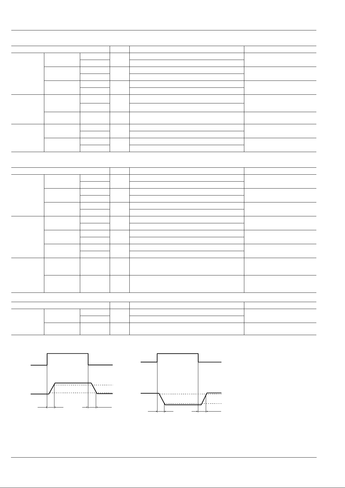
*Operate/Reverse time
For type of connection, see page 34.
Item Symbol AQS610TS Condition
Input
LED operate
current
Typical
I
Fon
0.9 mA
I
L
=Max.
Maximum 3 mA
LED reverse
current
Minimum
I
Foff
0.4 mA
I
L
=Max.
Typical 0.8 mA
LED dropout
voltage
Typical
V
F
1.14 (1.25 V at I
F
=50mA)
I
F
=5mA
Maximum 1.5 V
Output
On resistance
Typical
R
on
18 Ω
I
F
= 5 mA (N.O.), I
F
= 0 mA (N.C.)
I
L
= Max.
Within 1 s on time
Maximum 25 Ω
Off state leakage current
Maximum I
Leak
1 µ
A
I
F
= 0 mA (N.O.), I
F
= 5 mA (N.C.)
V
L
= Max.
Transfer char-
acteristics
Operate time*
Typical
T
on
0.23 ms (N.O.), 0.52 ms (N.C.)
I
F
= 0 mA → 5 mA
I
L
=Max.
Maximum 1.0 ms
Reverse time*
Typical
T
off
0.04 ms (N.O.), 0.23 ms (N.C.)
I
F
= 5 mA → 0 mA
I
L
=Max.
Maximum 1.0 ms
Item Symbol AQS610TS Condition
Input
LED operate
current
Typical
I
Fon
2 mA
I
C
= 2 mA
V
CE
= 0.5 V
Maximum 6 mA
LED turn off
current
Minimum
I
Foff
5 µ A
I
C
= 1 µ A
V
CE
= 5 V
Typical 35
µ
A
LED dropout
voltage
Typical
V
F
1.14 (1.25 V at I
F
= 50 mA)
I
F
= 5 mA
Maximum 1.5 V
Output
Saturation voltage
Typical
V
on
0.08 V
I
F
= 15 mA
I
C
= 2 mA
Maximum 0.5 V
Off state leakage current
Typical
I
CEO
0.01 nA
I
F
= 0
V
CE
= 5 V
Maximum 500 nA
Current transfer ratio
Minimum
—
33%
I
F
= 5 mA
V
CE
= 0.5 V
Typical 100%
Transfer char-
acteristics
Turn on time* Typical T
on
0.01 ms
I
F
= 5 mA
V
CE
= 5 V
I
C
=2 mA
Turn off time* Typical T
off
0.03ms
I
F
= 5 mA
V
CE
= 5 V
I
C
= 2 mA
Item Symbol AQS610TS Condition
Transfer char-
acteristics
I/O capacitance
Typical
C
iso
0.8pF
f = 1 MHz
V
B
= 0
Maximum 1.5pF
Initial I/O isolation resistance
Minimum R
iso
1,000M
Ω
500V DC
Ton
Input
Output 10%
90%
1) N.O. 2) N.C.
Toff
Toff
Input
Output
10%
90%
Ton
■
For Dimensions, see Page 28.
■
For Schematic and Wiring Diagrams, see Page 34.
■
For Cautions for Use, see Page 36.
 Loading...