

NAIS AQS210TSZ, AQS210TSX Datasheet
2 MOSFET Relay and
1 optocoupler type
4.4
1 MOSFET Relay and
10.37
.408
mm inch
1
2
3
4
5
6
7
8
Relay portion
(2,3,14,15,16 pins)
(4,5,11,12,13 pins)
Detector portion
(6,7,9,10 pins)
.173
2.1
2 optocouplers type
.083
16
15
14
13
12
11
10
9
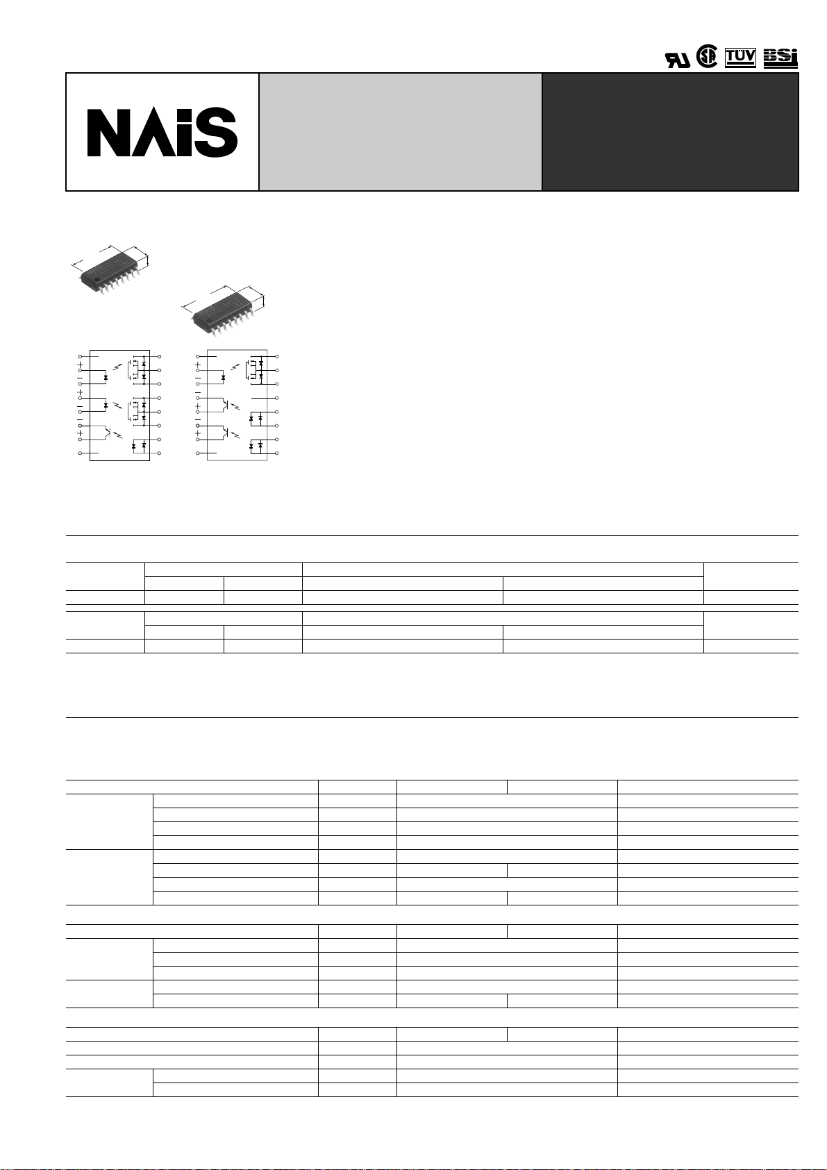
GU (General Use) Type
SOP Series
Multi-function (1a,2a MOSFET
& optocoupler) 16 Pin Type
4.4
10.37
.408
1
2
3
4
5
6
7
8
Relay portion
(2,3,14,15,16 pins)
Detector portion
(4,5,11,12 pins)
(6,7,9,10 pins)
.173
2.1
.083
FEATURES
1. SO package 16-Pin type in super
miniature design
The device comes in a super-miniature
SO package 16-Pin type measuring
(W)4.4 × (L)10.37 × (H) 2.1mm (W).173 ×
(L).408 × (H).083inch
2. Ideal for PC car d and Fax/Modem applications
16
The small size provides additional space
15
for increased functionality. The new de-
14
vice has been specifically designed for
13
the PCMCIA embedded and handheld
12
device markets.
11
10
3. Tape and reel
9
The device comes standard in a tape and
reel (1,000 pcs./reel) to facilitate automatic insertion machines.
AQS210TS, 210T2S
TESTING
PhotoMOS
RELAYS
TYPICAL APPLICATIONS
• PCMCIA Modem card (Data/fax modem)
• Laptop and notebook computers
• PDA's
• Mobile computing equipment
• Medical equipment
• Security systems
• Meters (Water, Gas, Vending machine)
TYPES
1 optocoupler
type
AC/DC type 350 V 100 mA AQS210TSX AQS210TSZ 1,000 pcs.
2 optocouplers
type
AC/DC type 350 V 120 mA AQS210T2SX AQS210T2SZ 1,000 pcs.
* Indicate the peak AC and DC values.
Notes: (1) Tape package is the standard packing style. Also available in tube. (Part No. suffix "X" or "Z" is not needed when ordering; Tube: 50 pcs.;
Case: 1,000 pcs.)
(2) For space reasons, the package type indicator "X" and "Z" are omitted from the seal.
Output rating* Part No.
Load voltage Load current Picked from the 1/2/3/4/5/6/7/8-pin side
Output rating* Part No.
Load voltage Load current Picked from the 1/2/3/4/5/6/7/8-pin side
Picked from the 9/10/11/12/13/14/15/16-pin side
Picked from the 9/10/11/12/13/14/15/16-pin side
Packing quantity
in tape and reel
Packing quantity
in tape and reel
RATING
1. Absolute maximum ratings (Ambient temperature: 25 ° C 77 ° F)
1) Relay portion (2, 3, 14, 15, 16 and 4, 5, 11, 12, 13 pins) [AQS210TS], (2, 3, 14, 15, 16 pins) [AQS210T2S]
Item Symbol AQS210TS AQS210T2S Remarks
LED forward current I
Input
Output
LED reverse voltage V
Peak forward current I
Power dissipation P
Load voltage V
Continuous load current I
Peak load current I
Power dissipation P
2) Detector portion (6, 7, 9, 10 pins) [AQS210TS], (4, 5, 11, 12 and 6, 7, 9, 10 pins) [AQS210T2S]
Item Symbol AQS210TS AQS210T2S Remarks
LED forward current I
Input
Output
Peak forward current I
Power dissipation P
Output voltage BV
Power dissipation P
3) Others
Item Symbol AQS210TS AQS210T2S Remarks
Total power dissipation P
I/O isolation voltage V
Temperature
limits
Operating T
Storage T
peak
F
R
FP
in
L
L
out
F
FP
in
CEO
out
T
iso
opr
stg
0.1A (0.12 A) 0.12A ( ) : in case of using only 1 channel
600mW 400mW
150mW 100mW
–40 ° C to +85 ° C –40 ° F to +185 ° F Non-condensing at low temperatures
–40 ° C to +100 ° C –40 ° F to +212 ° F
50mA
3V
1A f=100 Hz, Duty factor=0.1%
75mW
350V
0.36A 100 ms (1 shot), V
50mA
1A f = 100 Hz, Duty factor=0.1%
75mW
30V
650mW
1500V AC
L
= DC
89
AQS210TS, 210T2S
2. Electrical characteristics (Ambient temperature: 25 ° C 77 ° F)
1) Relay portion (2, 3, 14, 15, 16 and 4, 5, 11, 12, 13 pins) [AQS210TS] (2, 3, 14, 15, 16 pins) [AQS210T2S]
Item
Typical
Maximum 3mA
Minimum
Typical 0.8mA
Typical
Maximum 1.5V
Input
LED operate
current
LED turn off
current
LED dropout
voltage
Typical
Output
Transfer char-
acteristics
On resistance
Off state leakage current
Turn on time*
Turn off time*
Maximum 25 Ω
Maximum I
Typical
Maximum 1.0 ms
Typical
Maximum 1.0 ms
2) Detector portion (6, 7, 9, 10 pins) [AQS210TS] (4, 5, 11, 12 and 6, 7, 9, 10 pins) [AQS210T2S]
Item
Typical
Maximum 6mA
Minimum
Typical 35 µ A
Typical
Maximum 1.5V
Typical
Maximum 0.5V
Typical
Maximum 500nA
Minimum
Typical 100%
Input
Output
LED operate
current
LED turn off
current
LED dropout
voltage
Saturation voltage
Off state leakage current
Current transfer ratio
Turn on time* Typical T
Transfer char-
acteristics
Turn off time* Typical T
3) Others
Item
Typical
Maximum 1.5pF
Minimum R
Transfer char-
acteristics
I/O capacitance
Initial I/O isolation resistance
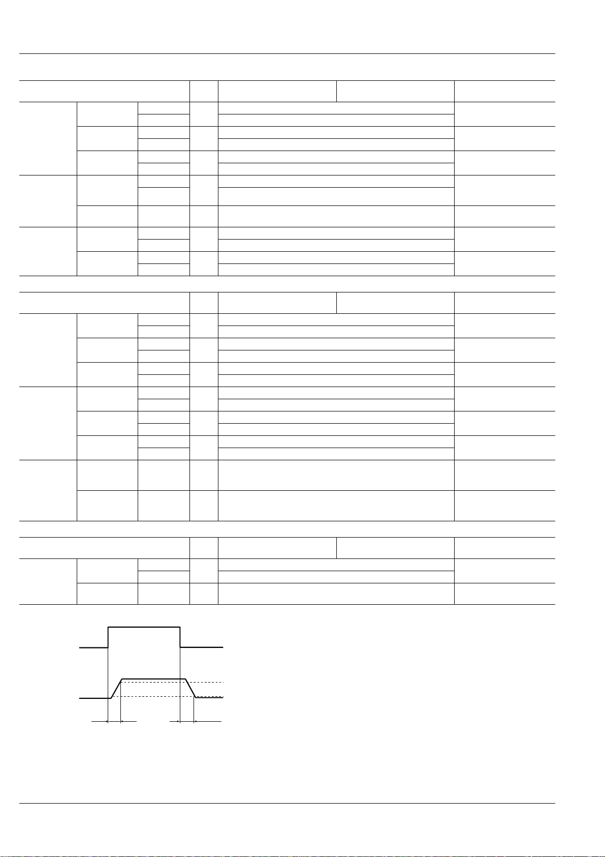
*Turn on/Turn off time
Sym-
bol
Fon
I
Foff
I
F
V
on
R
Leak
T
on
T
off
Sym-
bol
I
Fon
I
Foff
V
F
V
on
I
CEO
—
on
off
Sym-
bol
C
iso
iso
AQS210TS AQS210T2S Condition
0.9mA
0.4mA
1.14 (1.25 V at I
F
=50mA)
17 Ω
1 µ A
0.23ms
0.04ms
AQS210TS AQS210T2S Condition
2mA
5 µ A
1.14 (1.25 V at I
=50mA)
F
0.08V
0.01nA
33%
0.01ms
0.03ms
AQS210TS AQS210T2S Condition
0.8pF
1,000M Ω
For type of connection, see page 34.
■
■
■
Within 1 s on time
L
I
=Max.
L
I
=Max.
F
I
=5mA
I
=5mA
F
I
=Max.
L
I
=0
F
I
=Max.
L
I
=5mA
F
I
=Max.
L
I
=5mA
F
I
=Max.
L
I
=2mA
C
V
=0.5V
CE
I
=1 µ A
C
V
=5V
CE
I
=5mA
F
I
=15mA
F
I
=2mA
C
I
=0
F
V
=5V
CE
I
=5mA
F
V
=0.5V
CE
I
=5mA
F
V
=5V
CE
I
=2mA
C
I
=5mA
F
V
=5V
CE
I
=2mA
C
f =1 MHz
V
=0
B
500V DC
90
Input
90%
Output 10%
Ton
Toff
For Dimensions, see Page 28.
For Schematic and Wiring Diagrams, see Page 34.
For Cautions for Use, see Page 36.
 Loading...