

Page 1
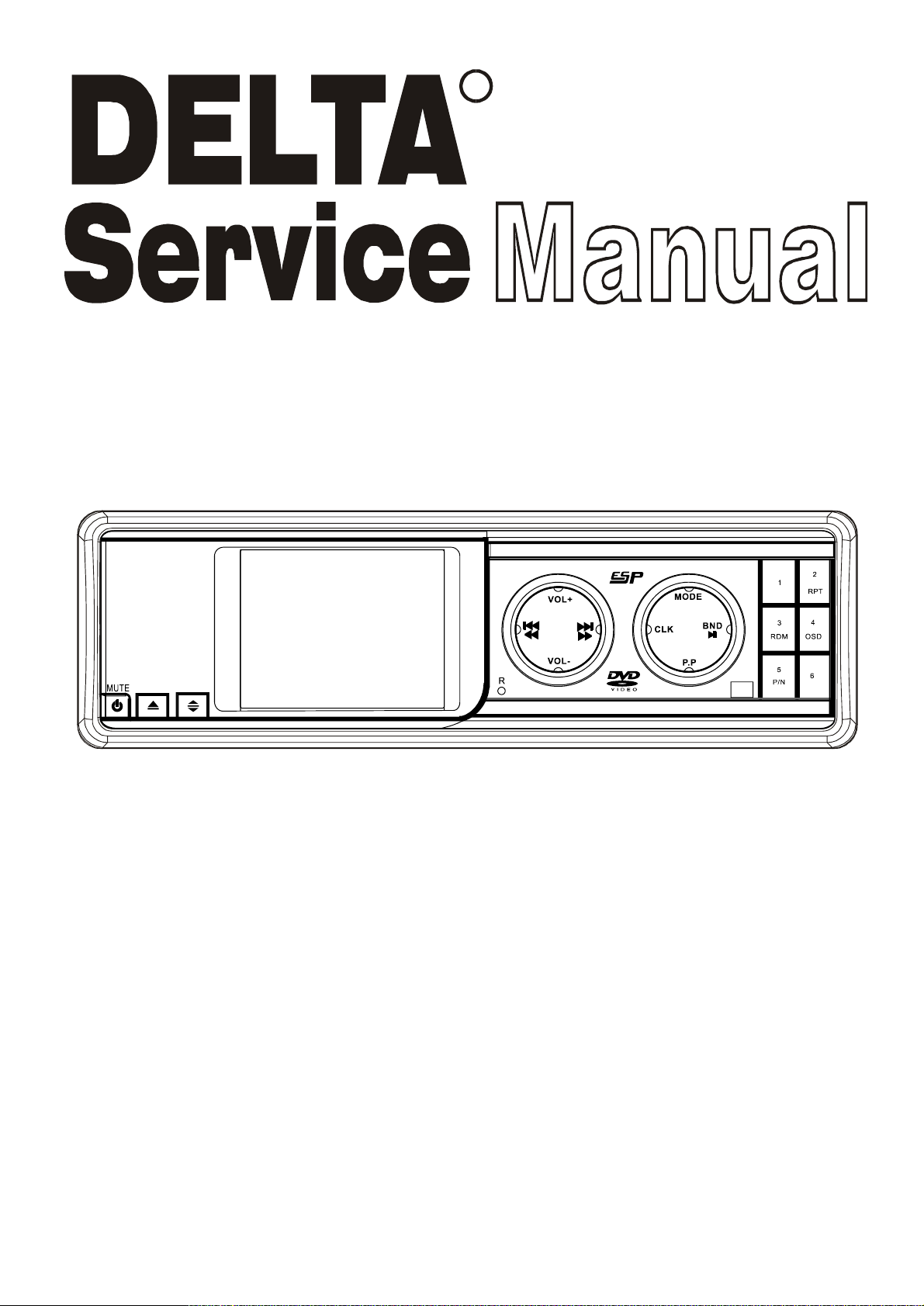
R
PLL SYNTHESIZER STEREO RADIO WITH
DVD/VCD/MP3/CD PLAYER DIGITAL
MODE:MMD-888
Page 2

CONTENTS
Page
Disassembly Instructions....................................................................................................3
Disassembly Diagram.........................................................................................................4
Operation Check................................................................................................................5
Block Diagram................................................................................................................ 6...
Alignment Locations...........................................................................................................7
Alignment Procedures........................................................................................................8
PrintedCircuit Boards.........................................................................................................9
Exploded Views (Panel)......................................................................................................15
Exploded ViewParts Lists (Panel).......................................................................................16
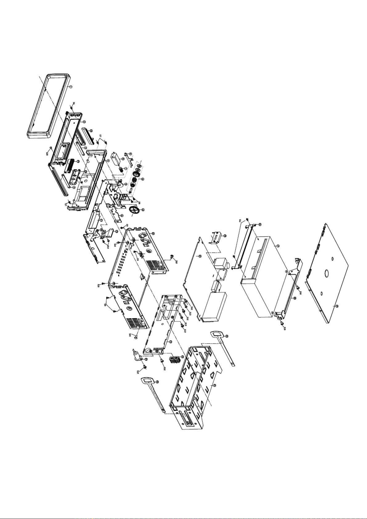
Exploded Views (Cabinet)..................................................................................................17
Exploded View Parts Lists(Cabinet).................................................................................... 18
Schematic Diagram............................................................................................................19
Electrical Parts List............................................................................................................25
Specifications....................................................................................................................29
2
Page 3

DISASSEMBLY INSTRUCTIONS
1. Using the unlock key that came with the unit or a similar tool, unlock the Mounting Box and remove
toward the read of the unit.
2. Remove two screws (A) located on the rear of the top cabinet then remove the Top Cabinet.
3. Remove two screw (B) located on the rear of the bottom cabinet then remove the Bottom Cabint.
4. Remove two screw (C) and (D) from the side bracket of the right side.
Remove the screw (E) and (F) from the side bracket of the left side.
5. Remove two screws (G) from the base of the front side then remove the two screws (H) loated unit
the front desk bracket then remove the Front Dect Bracket.
Remove two screws (I) located under the rear deck bracket then remove the Rear Deck Bracket.
6. Remove two screws (J) from the Heat Sink then remove the Spring Sheet.
7. Remove five screws (K) from the Heat Sink then remove the Heat Sink.
8. Remove two screws (L) located on the side bracket of the rear side then remove the ISO Antenna
Socket/Shore W/Holder.
9. Remove the screw (M) located on the side bracket of the rear side.
Remove two screws (N) located on the main board then remove the HeatSink (7809/DB435).
10. Remove the screw (O) located on the side bracket of the rear side then remove the 22PIN socket.
11. Take out the Panel and the Ring.
Remove two screws (P) from each side of the base then remove the Base.
12. Remove the screw (Q) located under the main board then remove the Main Board.
3
Page 4
DISASSEMBLY DIAGRAM
4
Page 5

OPERATION CHECK
GENERAL SPECIFICATIONS OF SIGNAL
Frequency range
OIRT
Intermediate frequency
Practicality neat(S/N 30dB)
Practicality neat(S/N 20dB)
Frequency Character
Signal/Noise Ratio
Channel
Power
FM
AM
FM 65-74MHz
FM
AM
FM Less than 22dB
AM
87.5, 108 MHz
522-1620 KHz
10.7 MHz
450 kHz
Less than 48dB
5-20,000Hz (+2dB)
70dB(1KHz)(1EC-A Network)
2 channels (stereo)
12-13.8V, -earth
The signal strength read in this section is voltage on the antenna.
Test Diagram
ANTENNA
SIDE BRAKE
B+ 12V
BACK CAMERA
VIDEO CONTROL
L(White)
AUX LINE INPUT
R(Red)
SUBWOOFER
(Green)
L(White)
RCALINE OUTPUT
R(Red)
VIDEO INPUT
(Yellow)
VIDEO OUTPUT
(Yellow)
Brown
Brown/white
Black
Black
Green
Brown
Brown
Yellow
Black
POWER
ANTENNA
AMPLIFIER
CONTROL
ACC +
FRONT
L SP
REAR
L SP
Blue
Blue/White
Red
+
White
-
White/Black
+
Green
-
Green/Black
Pink
DIMMER CONTROL
10A
Grey
Grey/Black
Purple
Purple/Black
UNIT
Yellow B+
Black B-
+
FRONT
R SP
-
+
REAR
R SP
-
-
+
5
Page 6

BLOCK DIAGRAM
6
Page 7

FM/MW/LW TUNER
ALIGNMENT LOCATIONS
7
Page 8

ALIGNMENT PROCEDURES
FM ADJUSTMENT
Equipment Required
AM IF/RF signal generator
Solid-state voltmeter (SSVM)
Regulated DC power supply
2-CH voltmeter
Distortion meter
FM Alignment Using FM Signal Generator
Note: Press the radio power switch to on the radio. Signal generator output must be kept as low as
possible to avoid overload and clipping.
Step
Stereo
separation
FM SNC
Adjustment
Stop
SENS.
Note: The tuner module is well-adjustand adjustemnt is not recommended.
Generator
coupling
Signal
Generator
to antenna
receptacle
98.1MHz
Dev. 75 khz
L+R=90%
Int. 1 khz
60dBuV output
Signal Generator
To antenna
receptale
Generator
98.1MHz
Int. 1 khz
Dev. 75 khz
L+R = 90 %
Pilot = 10 %
@
98.1 Mhz
Mod. 1kHZ
Dev 75kHz
Display
setting
98.1MHz
98.1MHz
98.1MHz
Adjustment Remarks
VR1
VR2
VR3
Adjust AF
output power
at maximum
separating
more than 30 dB
Stereo Separation
25 dB (+5dB)
Adjust AF to
stop station.
8
Page 9
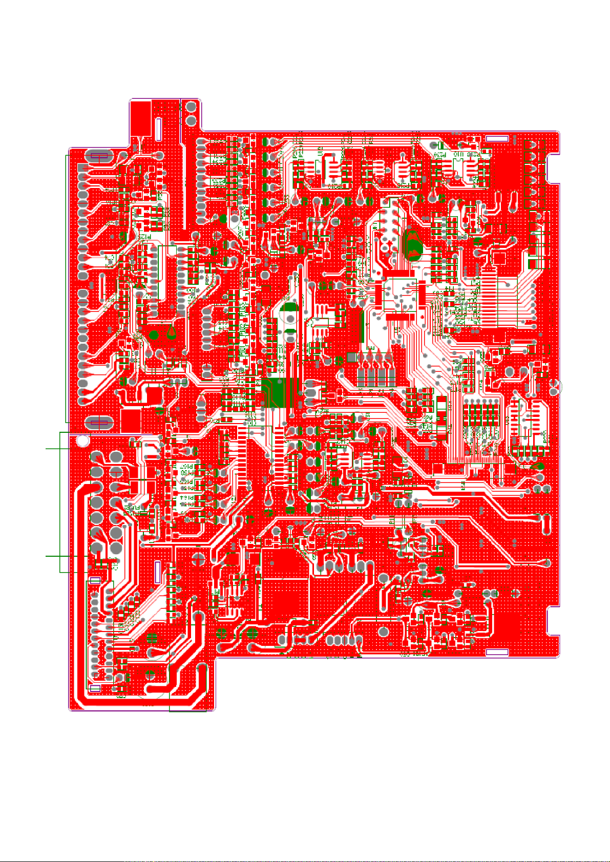
MAIN BOARD
PRINTED CIRCUIT BOARDS
TOP VIEW
9
Page 10

MAIN BOARD
BOTTOM VIEW
10
Page 11

KEY BOAR
TOP VIEW
11
Page 12

KEY BOARD
BOTTOM VIEW
12
Page 13

SERVO BOARD
TOP VIEW
13
Page 14

SERVO BOARD
BOTTOM VIEW
14
Page 15

PANEL
EXPLODED VIEW
15
Page 16

EXPLODED VIEW PARTS LIST
16
Page 17

CABINET
EXPLODED VIEW
17
Page 18

CABINET
EXPLODED VIEW PARTS LIST
18
Page 19

SCHEMATIC DIAGRAM(MAIN BOARD)
B
ATT
0.5A
FUSE2
FUSE3
0.5A
FUSE1
0.5A
L
AMP CONTROL
KB12V
C125 1000U
ZD14 12V
A2K
3
C42
47uF
C84104
HSD
20
6
25
ACGND
16
TAB
1
SVR
10
SGND
13
1
2
3
C124 474
C123
474
47uF
C44
19
1
000uF/10V
1
000uF/16V
Page 20

SCHEMATIC DIAGRAM(MAIN BOARD)
P
ANELCONNECTOR
KB_12V
KB12V
P2.2
P
1.1
3.3V
X OUT
DVCC
1
P6.3/A3
2
P6.4/A4
3
P6.5/A5
4
P6.6/A6
5
TB
TA
SW01
30
29
28
27
26
25
24
23
22
21
20
19
18
17
16
15
14
13
12
11
10
9
8
7
6
5
4
3
2
1
POWER_CON
XCS
XMC
XMD
IN_SW
DISK_SW
OUT_SW
AUDIO_DR
AUDIO_DL
AUDIO_FR
AUDIO_FL
AUDIO_SR
AUDIO_SL
AUDIO_SW
AUDIO_CE
VIDEO_B
VIDEO_G
VIDEO_R
TV-GND
CVBS
OPEN
CLOSE
P6.7/A7
6
VREF+
7
XIN
8
9
10
11
12
13
14
15
16
XOUT/TCLK
VeREF+
VREF-/VeREF-
P1.0/TACLK
P1.1/TA0
P1.2/TA1
P1.3/TA2
P1.4/SMCLK
P5.4/MCLK
48
P5.3
47
P5.2
46
P5.1
45
P5.0
44
P4.7/TBCLK
43
P4.6
42
P4.5
41
P4.4
40
P4.3
39
P4.2/TB2
38
P4.1/TB1
37
P4.0/TB0
36
P3.7
35
P3.6
34
P3.5/URXD0
33
R96 22K
22K
R87
20
Page 21

SCHEMATIC DIAGRAM(MAIN BOARD)
21
84 84 84
Page 22

SCHEMATIC DIAGRAM(MAIN BOARD)
84
6
5
4
3
2
1
22
Page 23

SCHEMATIC DIAGRAM(MAIN BOARD)
2
1
84
15
14
13
12
2
1
8
7
6
9
23
Page 24

Display Circuit
1
GND
2
GND
2
1
Y_SIG
TODISPPLAY
BS2
X
ENB
34
ENB
35
36
37
38
P
CD
39
40
BOUT
41
42
43
GOUT
44
45
ROUT
46
47
48
+3V3A
2
16 33
15
14
13
12
11
10
9
8
7
6
5
4
3
2
1
R37100R
100R
CE
R35
R75
47K
47K
R74
R73 47K
SCLK
DATA
N_TRAP
P_TRAP
Control Circuit
24
Page 25

ELECTRICAL PARTS LIST
* * * * * * * *KB board part* * * * * * *
Spare Number Spare Name Quantity Location
001-001117-033 IC AMS1117-3.3V 1 U4
001-004053-001
001-018P24-001
001-001380-001 IC AT1380AP tssop8 1 U6
001-004137-001 IC IV4137W SQFP64 1 U3
001-002651-001 IC LM2651MTC-ADJ 1 U2
002-002020-002 RED LED BLUE 0805 SMD
002-003020-06A SMT LED BLUE 0805 SMD
002-005817-001 DIODE 5817 D-58X
002-005819-001 DIODE 5819 D-58X
003-003904-001 AUDION
003-003400-001
003-000411-001
004-000443-004 Crystal Flap
004-000358-004 Crystal Flap
005-005160-020 CHIP CAP 16P/50V 0603 ð5% NPO
005-005390-020 CHIP CAP 39P/50V 0603 ð5% NPO
005-005820-020
005-005271-020 CHIP CAP 270P/50V 0603 ð5% NPO
005-005102-020
005-005222-020 CHIP CAP 222P/50V 0603 ð10% X7R
005-005472-020 CHIP CAP 472P/50V 0603 ð10% X7R
005-005682-020
005-005103-020
005-005333-020 CHIP CAP 333P/25V 0603 ð10% X7R
005-005473-020 CHIP CAP 473P/25V 0603 ð10% X7R
005-005104-020
005-005334-020 CHIP CAP 334P/25V 0603 ð20% Y5V
005-005474-020
005-005105-020
005-005106-01A
005-005226-01A
005-005336-01B
005-006107-00D Ta capacitance
006-250107-01D Ta capacitance
007-002100-020 CHIP RES
007-002360-020
007-002101-020 CHIP RES
007-002181-020 CHIP RES
007-002221-020 CHIP RES
007-002331-020
007-002471-020
007-002681-020
007-002102-020 CHIP RES 1K 0603 ð5% SMD
007-002152-020 CHIP RES 1.5K 0603 ð5% SMD
007-002222-020
007-002302-020
007-002332-020
007-002472-020 CHIP RES 4.7K 0603 ð5% SMD
007-002562-020
007-002822-020
007-002103-020 CHIP RES 10K 0603 ð5% SMD
007-002123-020
007-002153-020
007-002332-020
007-002473-020
007-002513-020
007-002334-020
IC 74HC4053M TSSOP-16 SMD 1 U5
IC MTV018P24-04 SO-24 SMD 1 U7
2N3904 SOT-23
AUDION
AUDION
CHIP CAP 82P/50V 0603 ð5% NPO
CHIP CAP
CHIP CAP 682P/50V
CHIP CAP 103P/50V
CHIP CAP
CHIP CAP
CHIP CAP 1uF/25V
CHIP CAP 10uF/16V
CHIP CAP 22uF/16V
CHIP CAP 33uF/16V
CHIP RES
CHIP RES
CHIP RES
CHIP RES
CHIP RES
CHIP RES
CHIP RES
CHIP RES
CHIP RES
CHIP RES
CHIP RES
CHIP RES
CHIP RES
CHIP RES
CHIP RES
AO3400 SOT-23
RB411D SOT-23 1 D6
4.433619MHz 49SS
3.579545MHz 49SS
102P/ 50V 0603
104P/ 25V 0603
474P/25V 0603
100uF/16V D type SMD
100uF/25V D type SMD
10
36 0603
100
180
220
330 0603
470 0603
680 0603
2K2 0603
3K 0603
3K3 0603
5K6 0603
8K2 0603
12K 0603
15K 0603
33K 0603
47K 0603
51K 0603
330K 0603
Spare Specification
SMD
SMD
SMD
SMD
SMD
SMD
ð10% X7R
0603
0603
0603
1206
1206
1210
0603 ð5% SMD
0603 ð5% SMD
0603 ð5% SMD
0603 ð5% SMD
ð10% X7R
ð10% X7R
ð10% X7R
ð20% Y5V
ð20% Y5V
ð20% Y5V
ð20% Y5V
ð20% Y5V
ð5% SMD
ð5% SMD
ð5% SMD
ð5% SMD
ð5% SMD
ð5% SMD
ð5% SMD
ð5% SMD
ð5% SMD
ð5% SMD
ð5% SMD
ð5% SMD
ð5% SMD
ð5% SMD
ð5% SMD
25
1 LD1
5 LD2-5,LED1a
1 D1
2 D2,3
1 Q1
1 Q2
1 X2
1 X1
2 C31,32
1 C47
1 C48
1 C52
1 C50
1 C22
1 C23
1 C49
4 C42-45
1 C29
1 C30
14 C1-9,39-41,54,55
1 C46
4 C35-38
6 C24-28,53
8 C10-17
1 C51
1 C34
2 C19,21
2 C18,20
1 R4
2 R67,68
7 R35,R37-39,R64-66
2 R5,6
2 R7,8
3 R9-11
2 R12,13
3 R14,15,21
7 R22-27,R1
2 R28,29
7 R2-3,R16-19,R1a
1 R78
2 R30,91
2 R31,92
3 R69,70,R72
2 R46,93
8 R51-57,R81
1 R76
3 R47,48,R82
1 R58
3 R73-75
4 R60-63
1 R77
Page 26

ELECTRICAL PARTS LIST - CONTINUED
*************** switchboard parts ***************
Spare Number Spare Name Quantity Location
072-009168-000 Motor 1
013-0013CR-002
013-0013CL-001
012-009168-009
Switch
Switch
Switch PCB
KCF-013CR 1
KFC-013CL 1
67X18X1.2MM 1
* * * * * * *main board parts* * * * * * * *
Spare Number Spare Name Quantity Location
001-072131-000 IC LC72131M
001-034063-001 IC MC34063
001-004558-001 IC RC4558 SOP8
001-007384-000 IC TDA7384
001-004053-001
01-DVD888-060114
001-007313-001 IC LP-7313 SMD
001-078M05-001 ZENER IC
001-078M08-001 ZENER IC
001-078M12-001 ZENER IC
001-000431-000
002-000030-002 LED
002-004007-000 DIODE IN4007
002-005401-000 DIODE 5401
002-004148-001 DIODE 4148
002-005819-001 DIODE 1N5819
002-005056-05A
002-005051-005
002-005056-005
002-005068-005
002-005100-005
002-005120-005
003-008050-000
003-008550-000
003-000882-000
003-001424-001
003-003906-001
003-008050-001 AUDION
003-008550-001
003-009015-001 AUDION 9015 SOT-23 400-1000 SMD
003-002955-000
004-032768-000 crystal oscillator
004-000045-000
005-000105-000 Ta capacitance 1uF/16V
005-005120-020
005-005270-020
005-005101-020
005-005221-020
005-005471-020
005-005102-020
005-005152-020
005-005222-020
005-005272-020
005-005332-020
005-005103-020
005-005153-020
005-005104-020 CHIP CAP
005-005474-020
IC 74HC4053M TSSOP-16 SMD
IC MSP430F007
78M05 5V SMD
78M08 8V SMD
78M12 12V SMD
TL431 Insert
3MM
ZENER DIODE
ZENER DIODE
ZENER DIODE
ZENER DIODE
ZENER DIODE
ZENER DIODE
AUDION
AUDION
AUDION
AUDION
AUDION
AUDION
AUDION
crystal oscillator
CHIP CAP
CHIP CAP
CHIP CAP 100P/50V
CHIP CAP 220P/50V
CHIP CAP
CHIP CAP
CHIP CAP
CHIP CAP
CHIP CAP
CHIP CAP
CHIP CAP 103P/50V
CHIP CAP
CHIP CAP
5.6V 0.5W
5.1V 0.5W
5.6V 0.5W
6V8 0.5W
10V 0.5W
12V 0.5W
S8050C TO-92 160-300
S8550D TO-92 120-200
D882
2SB1424 SOT-89
3906
8050 SOT-23 SMD
8550 SOT-23 SMD
9014AUDION003-009014-001
FD2955
32.768KHz
4.5MHz Insert
12P/50V 0603
27P/50V 0603
471P/50V 0603
102P/ 50V 0603
152P/ 50V 0603
222P/ 50V 0603
272P/ 50V 0603
332P/ 50V 0603
153P/ 50V 0603
104P/ 25V
474P/25V 0603
1uF/25VCHIP CAP005-005105-020
Spare Specification
Spare Specification
Insert
SMD
SMD
Insert
S-PQFP-G64
20MA Red
Insert
Insert
SMD
SMD
SMD
Insert
Insert
Insert
Insert
Insert
Insert
SMD
SMD
SMD200-600SOT-23
KX-327SP
0603
0603
0603
0603
0603
ð5% NPO
ð5% NPO
ð5% NPO
ð5% X7R
ð5% X7R
ð10% X7R
ð10% X7R
ð10% X7R
ð10% X7R
ð10% X7R
ð10% X7R
ð10% X7R
ð10% X7R
ð20% Y5V
Insert
Y5Vð20%
26
1 U3
1 U4
2 R9,U16
1 U7
1 U15
1 U5(888DTsol uti on)
1 U6
1 U13
1 U1
1 U2
IC
1 U8
1 LD1
5 D3,D7, D9, D10,D15
1 D11
7 D1,D2, D4-6,D13,D14
1 D12
11 ZD3-11, ZD17, ZD20
4 ZD1, ZD2,ZD18, ZD19
1 ZD16
1 ZD12
1 ZD13
1 ZD14
3 Q2, Q5,Q49
1 Q3
2 Q6, Q48
1 Q1
1 Q30
2 Q50,Q51
2 Q52,Q53
Q8-21,Q23,Q24, Q22,
25
Q31-36, Q43,Q45
3 Q25,Q26,Q28
1 Q7
1 X3
2 X1, X2
1 C4
2 C35, C36
4 C38- 41
2 C46, C47
1 C118
16 C62-65, C114-117,C127-134
3 C45, C60, C67
2 C90, C145
2 C108, C109
2 C110, C111
2 C141, C142
4 C112, C113, C71,C72
2 C146, C147
C73-89, C91-94, C97-
34
C102,C104, C105, C106, C136-
139
2 C123, C124
C5, C6, C8-15,C22,C23,
C5, C6, C8-15, C22,C23,
15
C26,C28, C201
Page 27

ELECTRICAL PARTS LIST ?CONTINUED
006-050104-004 E.CAP
006-050105-004 E.CAP 1uF/50V 4x5MM ð20%
006-016225-004 E.CAP 2.2uF/50V 4x5MM ð20%
006-016106-004 E.CAP 10uF/25V 4x5MM ð20%
006-016226-004 E.CAP 22uF/16V 5x5MM ð20%
006-016476-005 E.CAP 47uF/16V 5x5MM ð20%
006-016107-006 E.CAP 100uF/16V 6x5MM ð20%
006-016227-006 E.CAP 220uF/16V 8x5MM ð20%
006-016108-008
006-025228-010 E.CAP 2200uF/25V 10X30MM ð20%
007-005100-004 RES
007-005470-004
007-005101-002 RES
007-005101-004 RES
007-005221-004 RES
007-005332-004
007-002100-020 CHIP RES 10 0603
007-002220-020
007-002101-020 CHIP RES 100 0603
007-002151-020 CHIP RES 150 0603
007-002221-020 CHIP RES 220 0603
007-002331-020 CHIP RES 330 0603
007-002681-020 CHIP RES 680 0603
007-002102-020 CHIP RES 1K 0603
007-002182-020 CHIP RES 1.8K 0603
007-002302-020 CHIP RES
007-002332-020 CHIP RES
007-002472-020 CHIP RES
007-002562-020 CHIP RES
007-002682-020 CHIP RES 6.8K 0603 ð5% SMD
007-002822-020 CHIP RES 8.2K 0603 ð5% SMD
007-002103-020 CHIP RES
007-002153-020 CHIP RES 15K 0603
007-002223-020 CHIP RES 22K 0603
007-002273-020 CHIP RES 27K 0603
007-002333-020 CHIP RES 33K 0603
007-002393-020 CHIP RES 39K 0603
007-002473-020 CHIP RES 47K 0603
007-002104-020 CHIP RES 100K 0603
007-002124-020 CHIP RES 120K 0603
007-002154-020 CHIP RES 150K 0603
007-002224-020 CHIP RES 220K 0603
007-004103-005 10K resistance SE4.103A 5 PIN
009-003000-000
009-025033-010
009-104221-00A chip power inductance DS1204-221M 220uH 0.5X10.5MM
009-181005-001 inductance loop No seat 1 L2
012-DVD888-000
029-000021-001 Tuner MG-21FA
033-000005-001 Fuse 0.5A SMD
019-00905A-001 buzzer SHS-0905A
Spare Number Spare Name Quantity Location
001-003355-001 IC ALi M3355 SMD 1 U1
001-005954-001 IC BA5954FP SMD 1 U2
001-006289-001 IC BA6289F ROHM SMD 1 U3
001-001604-001 IC 1MX16X4Bank SMD 1 U4
E.CAP
RES
RES
CHIP RES
CHIP RES007-002222-020
i nductance
i nductance
PCB 170.5ð137ð1.6MM
0.1uF/ 50V 4x5MM
1000uF/16V 8X16MM
10
47 1/4W
100
100
220
3.3K 1/4W
22
2.2K
3K
3.3K
4.7K
5.6K
10K
FB ? 3MM ð 0.5 Insert
3.3uH 2.5MM
* * * * * * SERVO BOARD PARTS* * * * * *
1/4W ð5%
1/2W ð5%
1/4W ð5%
1/4W ð5%
0603 ð5% SMD
0603
0603
0603
0603
0603
0603
Spare Specification
ð20%
ð20%
ð5%
ð5%
ð5% SMD
ð5% SMD
ð5% SMD
ð5% SMD
ð5% SMD
ð5% SMD
ð5% SMD
ð5% SMD
ð5% SMD
ð5% SMD
ð5% SMD
ð5% SMD
ð5% SMD
ð5% SMD
ð5% SMD
ð5% SMD
ð5% SMD
ð5% SMD
ð5% SMD
ð5% SMD
ð5% SMD
ð5% SMD
ð5% SMD
resistance
-20 +105
-20 +105
-20 +105
-20 +105
-20 +105
-20 +105
-20 +105
-20 +105
-20 +105
-20 +105
SMDð5%
Insert
2 C95,C96
7 C1-3,C25,C27,C30, C34
4 C16-C19
5 C20,C24,C31-33
2 C7,C218
3 C42-C44
12 C50-57, C59, C235, C236, C237
3 C68,C121, C122
3 C119, C120,C125
1 C126
1 R80
1 R114
1 R140
3 R43,R132, R170
1 R142
1 R30
1 R81
1 R82
10 R3, R24,R26,R25,R196, R133-136,R27
1 R171
1 R143
5 R173, R186-189
1 R174
14 R1, 2, R4-11, R155- 158
2 R152, R153
R13,R15, R17,R18-R21,R28,
11
R29,R201,R202
1 R154
4 R31-34
8 R39-42, R180- 183
4 R44,R46,R47,R210
4 R35-38
2 R159, R160
R14,R50-72, R75-79, R87,
35
R94,R95, R96, R184, R185
4 R85,R86,R168,R169
13 R88-93, R97, R98, R100,R161,R175-177
4 R118, R127-129
2 R110, R111
1 R102
17 R119-126,R130, R162- 167,R236, R237
5 R83,R103, R137,R138,R139
4 R105- 108
1 R141
1 R84
RN1
1
2 L3,L5
1 L1
1 L4
mainboard
1
1 TUN1
3 FUSE1,2 ,3
1 S2
27
Page 28

ELECTRICAL PARTS LIST - CONTINUED
001-008766-001 IC WM8766 SSOP SMD 1 U8(use indoing 5.1)
001-008728-001 IC WM8728 SSOP SMD 1 U9
001-000MCU-001 IC MCU SMD 1 U10
001-001117-018 ZENER IC 1117/1V8 SOT223 1A SMD 1 Q7
001-001117-033 ZENER IC 1117/3V3 SOT223 1A SMD 1 Q8,
001-078L05-000
002-004148-001
002-004004-001
002-005822-001
002-005620-05A
002-000144-000 infrared transmitting tube
003-003904-001 AUDION 2N3904 SOT-23 SMD 2 Q2,Q1
003-003018-001 AUDION 2SK3018 SOT-23 SMD 2 Q4,Q3
003-001132-001 AUDION 2SB1132 SOT89 SMD 2 Q6,Q5
004-000027-000
005-005330-020 CHIP CAP 33P/50V 0603 ð5% NPO 2 C2,C3
005-005470-020 CHIP CAP 47P/50V 0603 ð5% NPO 1 C1
005-005101-020 CHIP CAP 100P/50V 0603 ð5% NPO 2 C29,C30
005-005271-020 CHIP CAP 270P/50V 0603 ð5% NPO 2 C35,C37
005-005331-020 CHIP CAP 330P/50V 0603 ð5% NPO 2 C36,C5
005-005391-020 CHIP CAP 390P/50V 0603 ð5% NPO 1 C9
005-005471-020 CHIP CAP 470P/50V 0603 ð5% NPO 8 C7,C8,BC8,BC16,C21,C22,C24,C25
005-005501-020 CHIP CAP 500P/50V 0603 ð5% NPO 2 C17,C18
005-005561-020 CHIP CAP 560P/50V 0603 ð5% NPO 1 C14
005-005102-020 CHIP CAP 102P/50V 0603 ð10% X7R 8 C10,C11,C12,C13,C19,C20,C33,C34
005-005472-020 CHIP CAP 472P/50V 0603 ð10% X7R 1 C31
005-005103-020 CHIP CAP 103/50V 0603 ð10% X7R 4 BC2,BC3,BC5,C15
005-005104-020 CHIP CAP
005-005224-020 CHIP CAP
005-005105-020 CHIP CAP 1uF/25V
006-016105-001 aluminum electrolytic capacitors 1U/16V ð20%
006-016106-001 aluminum electrolytic capacitors 10U/16V ð20%
006-016476-001 aluminum electrolytic capacitors 47U/16V ð20%
006-025476-001 aluminum electrolytic capacitors 47U/25V ð20%
006-016107-001 aluminum electrolytic capacitors 100U/16V ð20%
007-000101-001 chip resistance 100R 8PIN 4R SMD 2 RN2,RN1
007-000330-001 chip resistance 33R 8PIN 4R SMD 2 RN3,RN4
007-002000-020
007-002100-020
007-002220-020
007-002330-020 CHIP RES
007-002750-020
007-002221-020
007-002511-020
007-002681-020
007-002102-020
007-002152-020
007-002222-020
007-002332-020
007-002472-020
007-002682-020
007-002822-020
ZENER IC
DIODE
DIODE
DIODE
ZENER DIODE
crystal oscillator
CHIP RES
CHIP RES
CHIP RES
CHIP RES
CHIP RES
CHIP RES
CHIP RES
CHIP RES
CHIP RES
CHIP RES
CHIP RES
CHIP RES
CHIP RES
CHIP RES
78L05 small bulk insert
1N4148 SMD 10 D1,D2,D3,D4,D5,D7,D8,D21,D22,D23
1N4004 SMD 1 D6
1N5822 SMD 2 D10,D9
6.2V 0.5W SMD 1 ZD1
BIR-NM23C1 DM3mm 2 IR1,IR2
27MHz 49S 1 Y1
104P/ 25V
224P/25V 0603
0
10
22
33
75
220
510
680
1K 0603 ð5% SMD 7 R15,R50,R51,R54,R55,R47,R92
1.5K 0603 ð5% SMD 2 R41,R39
2.2K 0603 ð5% SMD 3 R14,R16,R17
3.3K 0603 ð5% SMD 1 R31
4.7K 0603 ð5% SMD 7 R9,R61,R67,R59,R65,R74,R75
6.8K 0603 ð5% SMD 1 R32
8.2K 0603 ð5% SMD 1 R13
0603
0603
0603 ð5% SMD 6 R33,R78,R79,R82,R12,R91
0603 ð5% SMD 2 R53,R52
0603 ð5% SMD 1 R5
0603 ð5% SMD 11
0603 ð5% SMD 1 R77
0603 ð5% SMD 1 R19
0603 1% SMD 1 R4
0603 ð5% SMD 2 R57,R56
ð10% X7R 60
ð20% Y5V 1 C6
ð20% Y5V 8
-20 +105
-20 +105
-20 +105
-20 +105
-20 +105
SMD 2 TC4,TC3
SMD 3 TC2,TC6,TC25
SMD 9
SMD 2 TC11,TC24
SMD 12
1 U6
C4,C16,C27,C32,C38,BC1,BC4,BC6,B
C7, BC9-BC15,BC18, BC19BC45,BC47,BC49,BC52,BC56-BC68
BC17,BC46,BC48,BC50,BC51,BC53,B
C54,BC55
TC1,TC12,TC13,TC17,TC23,TC26,TC
29,TC28, TC27
TC5,TC7,TC8,TC9,TC10,TC14,TC15,T
C16,TC18,TC19,TC20,TC22
R2,R6,R25,R71,R72,R85,R86,R87,R88,
R89, R90
28
Page 29

SPECIFICATIONS
T.H.D................................................................................................................Less than 0.35%
Signal to Noise Radio..........................................................................................More than 60dB
Channel Separation.............................................................................................More than 60dB
Frequency Response..............................................................................................20Hz - 20kHz
Stereo Separating(FM)..........................................................................................30dB(at 1kHz)
Singnalto Noise Ratio(FM).................................................................................Better than 50dB
Output Power..................................................................................................................4X40W
Speaker Output Impedance.........................................................................................4 To 8 ohm
Power Source.......................................................................................DC 12V, Negative ground
Frequency Range...........................................................................................FM 87.5-108.0MHz
.......................................................................................................................MW 522-1620kHz
..........................................................................................................................LW 144-288kHz
Sensitivity......................................................................................................FM 3uV(S/N=30dB)
.................................................................................................................MW32dBu(S/N=20dB)
..................................................................................................................LW35dBu(S/N=20dB)
Specifications are subject to change without notice.
29
Page 30

 Loading...