MYSON MTV24LC08-1, MTV24C08, MTV24C08-1, MTV24LC08 Datasheet

MYSON
TECHNOLOGY
MTV24C08/
24LC08
(Preliminary)
2-Wire 8912-Bit Serial CMOS EEPROM
This datasheet contains new product information. Analog Technology reserves the rights to modify the product specification without notice.
No liability is assumed as a result of the use of this product. No rights under any patent accompany the sale of the product.
MTV24C08/24LC08 Revision.1.0 11/03/1999
1/15
FEATURES
• State- of- the- Art Architecture
- Non-volatile data storage
- Standard Voltage and Low Voltage Operation
5.0(Vcc = 4.5V to 5.5V) for MTV24C08
3.0(Vcc = 2.7V to 5.5V) for 24LC08
• 2 wire I2C serial interface
- Provides bidirectional data transfer protocol
• 16-byte page write mode
- Minimizes total write time per word
• Self-timed write-cycle(including auto-erase)
• Durable and Reliable
- 10 years data retention after 1000K write/erase cycles
- Minimum of 1,000,000 write/erase cycles per word
- Unlimited read cycles
- ESD protection
• Low standby current
GENERAL DESCRIPTION
The MTV24C08/24LC08 is a low cost, non-volatile, 4096-bit serial EEPROM with enhanced security device
and conforms to all specifications in I2C 2 wire protocol. The whole memory can be disabled (Write
Protected) by connecting the WP pin to Vcc. This section of memory then becomes unalterable unless WP
is switched to Vss. It is enhanced with security function. Every word of the memory has a programmable
security bit to permit whether it can be altered or not. The MTV24C08/24LC08's communication protocol
uses CLOCK(SCL) and DATA I/O(SDA) lines to synchronously clock data between the master (for example
a microcomputer)and the slave EEPROM devices(s) .In addition, the bus structure allows for a maximum of
16K of EEPROM memory. This supports the family in 2K, 4K, 8K, 16K devices, allowing the user to
configure the memory as the application requires with any combination of EEPROMs (not to exceed 16K).
MTV EEPROMs are designed and tested for application requiring high endurance, high reliability, and low
power consumption.

MYSON
TECHNOLOGY
MTV24C08/
24LC08
(Preliminary)
MTV24C08/24LC08 Revision.1.0 11/03/1999
2/15
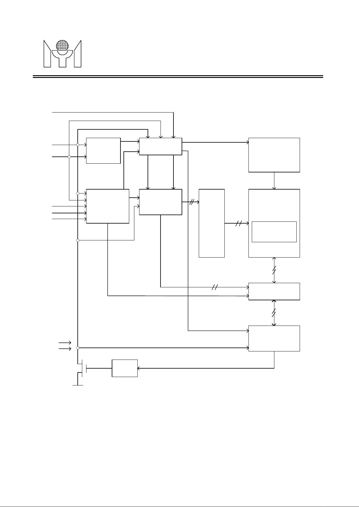
BLOCK DIAGRAM
START
STOP
LOGIC
CONTROL
LOGIC
SLAVE
ADDRESS
REGISTER
&
COMPARATOR
WORD
ADDRESS
COUNTER
H.V.
GENERATION
TIMING
&
CONTROL
XDEC
EEPROM
ARRAY
DATA
BIT
64X16X8
YDEC
DATA
REGISTER
DOUT
ACK
WP
SDA
SCL
A0
A1
A2
VCC
VSS
Din
R/W ~ , device address bit A0
4
Dout
128
64
6
incload
ck
start cycle
128

MYSON
TECHNOLOGY
MTV24C08/
24LC08
(Preliminary)
MTV24C08/24LC08 Revision.1.0 11/03/1999
3/15
PIN DESCRIPTIONS
SERIAL CLOCK (SCL)
The SCL input is used to clock all data into and out of the device.
SERIAL DATA (SDA)
SDA is a bidirection pin used to transfer data or security bit into and out of the device.
It is an open drain output and may be wire-ORed with any number of open drain or open collector outputs.
Thus, the SDA bus requires a pull-up resistor to Vcc (typical 4.7K£[ for 100KHZ, 1K£[ for 400KHZ)
DEVICE ADDRESS INPUTS (A0, A1, A2)
Device address pin A2 are connected to Vcc or Vss to configure the EEPROM address.
The following table (Table A) shows the active pins across the 24C/LCXX device family.
TABLE A
Device A0 A1 A2
24C02/24LC02 ADR ADR ADR
24C04/24LC04 XP ADR ADR
MTV24C08/24LC08 XP XP ADR
24C016/24LC016 XP XP XP
ADR indicates the device address pin.
XP indicates that device address pin don’ t care but refers to an internal PAGE BLOCK memory segment.
WRITE PROTECTION (WP)
If WP is connected to Vcc, PROGRAM operation onto the whole memory will not be executed. READ
operations are possible. If WP is connected to Vss, normal memory operation is enabled, READ/WRITE
over the entire memory is possible.
1.0 FUNCTIONAL DESCRIPTION
1.1 APPLICATIONS
MTV’ s electrically erasable programmable read only memories (EEPROMs) offer valuable security features
including write protect function , two write modes ,three read modes, and a wide variety of memory size.
Typical applications for the I2C bus and 24C/LCXX memories are included in SANs(small-area-networks),
stereos, televisions, automobiles and other scaled-down systems that don't require tremendous speeds but
instead cost efficiency and design simplicity.
1.2 ENDURANCE AND DATA RETENTION
The MTV24C08/24LC08 is designed for applications requiring up to 1,000,000 programming cycles (BYTE
WRITE and PAGE WRITE). It provides 10 years of secure data retention, without power after the execution
of 1,000,000 programming cycles.
1.3 DEVICE OPERATION

MYSON
TECHNOLOGY
MTV24C08/
24LC08
(Preliminary)
MTV24C08/24LC08 Revision.1.0 11/03/1999
4/15
The MTV24C08/24LC08 support a bi-directional bus oriented protocol. The protocol defines any device that
sends data onto the bus as a transmitter and the receiving device as the receiver. The device controlling the
transfer is the master and the device that is controlled is the slave. The master will always initiate data
transfers and provide the clock for both transmit and receive operations. Therefore, the MTV24C08/24LC08
is considered a slave in all applications.
Clock And Data Conventions
Data states on the SDA line can change only during SCL LOW. SDA state changes during SCL HIGH are
reserved for indicating start and stop conditions. (Shown in Figures 1 and 2)
Start Condition
A HIGH to LOW transition of the SDA line while the clock (SCL) is HIGH determines a START condition. All
commands must be preceded by a START condition. (Shown in Figure 2)
Stop Condition
A LOW to HIGH transition of the SDA line while the clock (SCL) is HIGH determines a STOP condition. All
operations must be ended with a STOP condition. (Shown in Figure 2)
Acknowledge
Each receiving device, when addressed, is obliged to generate an acknowledge after the reception of each
byte. The master device must generate an extra clock pulse which is associated with this acknowledge bit.
The device that acknowledges, has to pull down the SDA line during the acknowledge clock pulse in such a
way that the SDA line is stable LOW during the HIGH period of the acknowledge related clock pulse. Of
course, setup and hold times must be taken into account. A master must signal an end of data to the slave
by not generating an acknowledge bit on the last byte that has been clocked out of the slave. In this case,
the slave must leave the data line HIGH to enable the master to generate the STOP condition. (Shown in
Figure 3)
Devices Addressing
After generating a START condition, the bus master transmits the slave address consisting of a 4-bit device
code (1010) for the MTV24C08/24LC08, 3-bit device address (A2 A1 A0) and 1-bit value indicating the read
or write mode. All I2C EEPROMs use and internal protocol that defines a PAGE BLOCK size of 8K bits. The
MTV24C08/24LC08 contains four 2K-bits PAGE BLOCK, and the device address bits A0 and A1 are used
for determinating which PAGE BLOCK of memory segment the read/write operation will be proceeded in.
The eighth bit of slave address determines if the master device wants to read or write to the
MTV24C08/24LC08. (Refer to table B).
The MTV24C08/24LC08 monitor the bus for its corresponding slave address all the time. It generates an
acknowledge bit if the slave address was true and it is not in a programming mode.
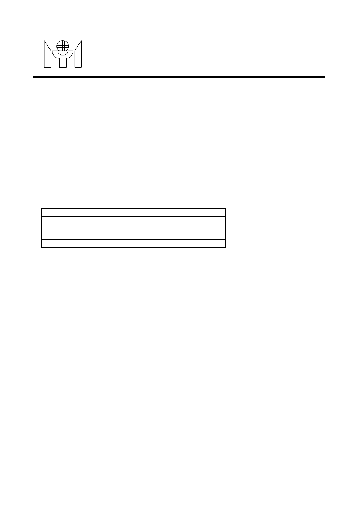
TABLE B
Operation Control Code Chip Select R/W
Read
Write
1010
1010
A2 A1 A0
A2 A1 A0
1
0
A2 are used to access device address for MTV24C08/24LC08, 8K bits’ size device.
A0 ,A1are used to access page blocks ,size of 8K bits, in the MTV24C08/24LC08

MYSON
TECHNOLOGY
MTV24C08/
24LC08
(Preliminary)
MTV24C08/24LC08 Revision.1.0 11/03/1999
5/15
WRITE OPERATIONS
Byte Write
Following the start signal from the master, the slave address is placed onto the bus by the
master transmitter. This indicates to the addressed slave receiver that a byte with a word address will follow
after it has generated an acknowledge bit during the ninth clock cycle.
Therefore the next byte transmitted by the master is the word address and will be written into the address
pointer of the MTV24C08/24LC08. After receiving another acknowledge signal from the MTV24C08/24LC08
the master device will transmit the data word to be written into the addressed memory location. The
MTV24C08/24LC08 acknowledges again and the master generates a stop condition. This initiates the
internal write cycle, and during this period the MTV24C08/24LC08 will not generate acknowledge signals.
(Shown in Figure 4)
Page Write
The write control byte, word address and the first data byte are transmitted to the MTV24C08/24LC08 in the
same way as in a byte write. But instead of generating a stop condition the master transmit up to 16 data
bytes to the MTV24C08/24LC08 which are temporarily stored in the on-chip page buffer and will be written
into the memory after the master has transmitted a stop condition. After the receipt of each byte, the two
lower order address pointer bits are internally incremented by one. The higher order six bits of the word
address remains constant. If the master should transmit more than 16 bytes prior to generating the stop
condition, the address counter will roll over and the previously received data will be overwritten. As with the
byte write operation, once the stop condition is received an internal write cycle will begin. (Shown in Figure
5).
Acknowledge Polling
Since the device will not acknowledge during a write cycle , this can be used to determine when the cycle is
complete (this feature can be used to maximize bus throughout). Once the stop condition for a write
command has been issued from the master, the device initiates the internally timed write cycle. ACK polling
can be initiated immediately. This involves the master sending a start condition followed by the control byte
for a write command (R/W = 0). If the device is still busy with the write cycle , then no ACK will returned. If
the cycle is complete then the device will return the ACK and the master can then proceed with the next
read or write commands.
Write Protection
Programming will not take place if the WP pin of the MTV24C08/24LC08 is connected to Vcc. The
MTV24C08/24LC08 will accept slave and byte addresses; but if the memory accessed is write protected by
the WP pin, the MTV24C08/24LC08 will not generate an acknowledge after the first byte of data has been
received, and thus the programming cycle will not be started when the stop condition is asserted.
READ OPERATIONS
Read operations are initiated in the same way as write operations with the exception that the R/W bit of the
slave address is set to one. There are three basic types of read operations: current address read, random
read, and sequential read.
 Loading...