

MYSON MTV112MV32 Datasheet
MYSON
-bytes internal RAM.
32K-bytes program Flash ROM.
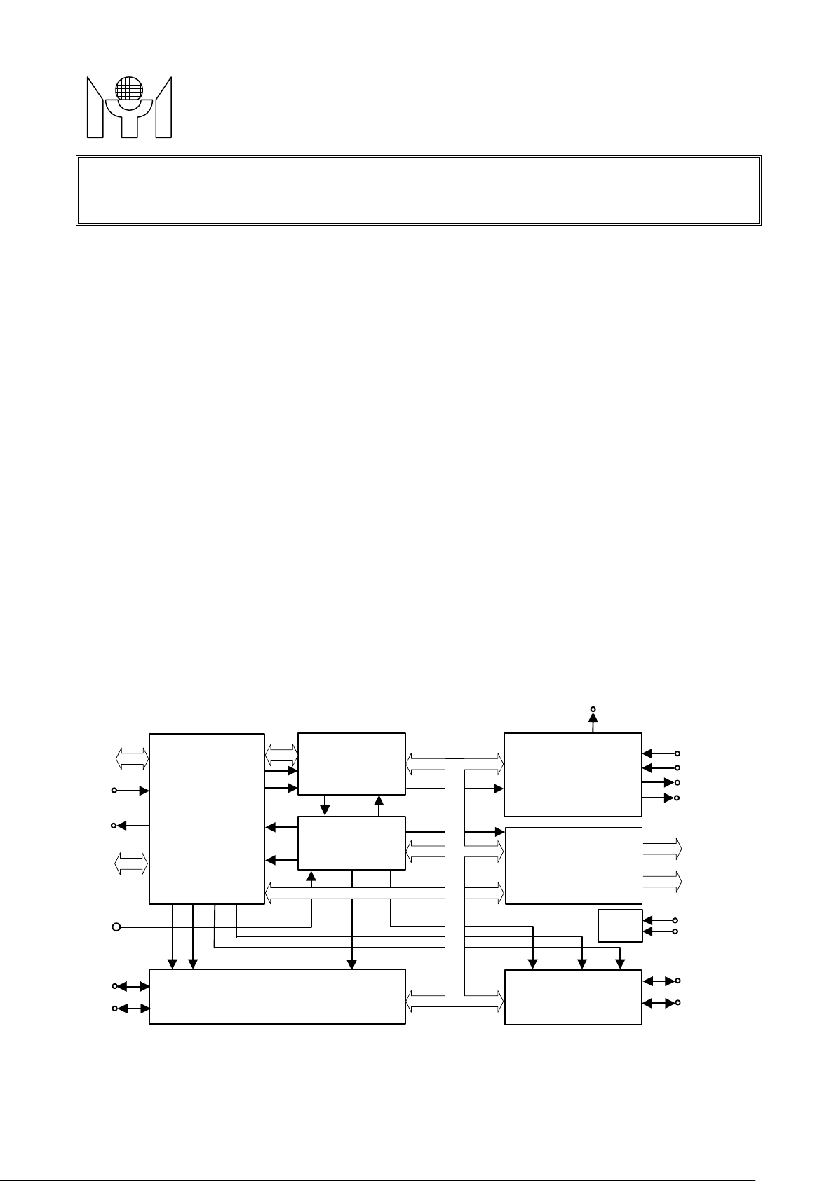
The MTV112M micro-controller is an 8051 CPU core embedded device specially tailored to CRT monitor
24Cxx series EEPROM interface, A/D converter and a 32K bytes internal program Flash ROM.
MTV112M
TECHNOLOGY
(Rev 2.0)
8051 Embedded CRT Monitor Controller
Flash Version
FEATURES
l 8051 core.
l 384
l
l 14-channels 5V open-drain PWM DAC, 10 dedicated channels and 4 channels shared with I/O pin.
l 28 bi-direction I/O pin,12 dedicated pin,12 shared with DAC, 4 shared with DDC/IIC interface.
l 3-output pin shared with H/V sync output and self test output pins.
l SYNC processor for composite separation, polarity and frequency check, and polarity adjustment.
l Built-in monitor self-test pattern generator.
l Built-in low power reset circuit.
l One slave mode IIC interface and one master mode IIC interface.
l IIC interface for DDC1/DDC2B and EEPROM, only one EEPROM needed to store DDC1/DDC2B and
display mode information.
l Dual 4-bit ADC or 4 channel 6-bit ADC.
l Watchdog timer with programmable interval.
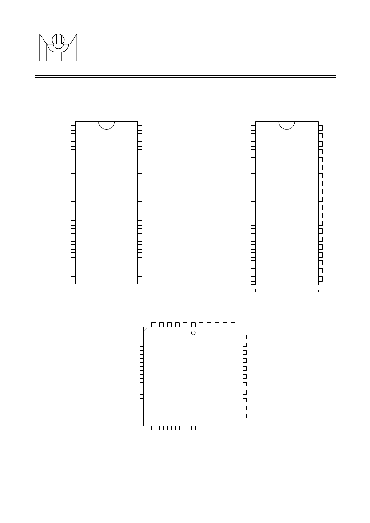
l 40-pin PDIP and 44-pin PLCC package.
GENERAL DESCRIPTION
applications. It includes an 8051 CPU core, 384-byte SRAM, 14 built-in PWM DACs, DDC1/DDC2B interface,
BL OCK DIAGRAM
STOUT
P1.0-7
X1
X2
P2.0-3
P3.0-P3.2
8051
CORE
P3.4
P0.0-7
RD
WR
INT
1
RST
P2.4-7
P0.0-7
XFR
RD
WR
WATCH-DOG
TIMER
RST
H / VSYNC
CONTROL
14 CHANNEL
PWM DAC
HSYNC
VSYNC
HBLANK
VBLANK
DA0-9
DA10-13
ADC
AD0
AD1
HSCL
HSDA
This datasheet contains new product information. Myson Technology reserves the rights to modify the product specification without
notice. No liability is assumed as a result of the use of this product. No rights under any patent accompany the sale of the product.
Revision 2.0 - 1 - 2001/05/18
DDC 1/2 B & FIFO
INTERFACE
IIC INTERFACE
ISCL
ISDA
MYSON
MTV112M
TECHNOLOGY
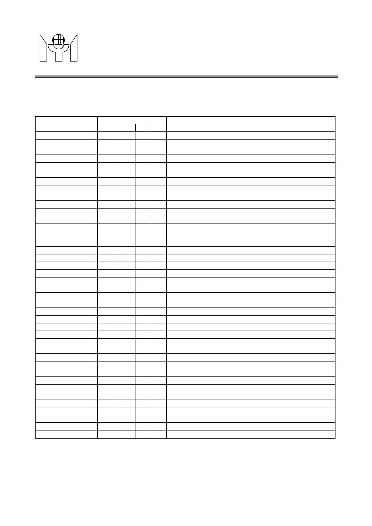
1.0 PIN CONNECTION
P1.0
P1.1/HALFV
P1.2/HALFH
P1.3/HCLAMP
P1.4/AD2
P1.5/AD3
P1.6/AD0
P1.7/AD1
RST
HSCL/P3.0/Rxd
HSDA/P3.1/Txd
ISDA/P3.2/INT0
HSYNC
ISCL/P3.4/T0
VSYNC
HBLANK/P4.1
VBLANK/P4.0
X2
X1
VSS
MTV112M
VDD
DA0/P5.0
DA1/P5.1
DA2/P5.2
DA3/P5.3
DA4/P5.4
DA5/P5.5
DA6/P5.6
DA7/P5.7
DA8
DA9
STOUT/P4.2
DA10/P2.7
DA11/P2.6
DA12/P2.5
DA13/P2.4
P2.3
P2.2
P2.1
P2.0/INT0
(Rev 2.0)
P1.0
P1.1/HALFV
P1.2/HALFH
P1.3/HCLAMP
P1.4/AD2
P1.5/AD3
P1.6/AD0
P1.7/AD1
RST
HSCL/P3.0/Rxd
HSDA/P3.1/Txd
ISDA/P3.2/INT0
HSYNC
ISCL/P3.4/T0
VSYNC
NC
HBLANK/P4.1
VBLANK/P4.0
VSS
X2
X1
MTV112M
VDD
DA0/P5.0
DA1/P5.1
DA2/P5.2
DA3/P5.3
DA4/P5.4
DA5/P5.5
DA6/P5.6
DA7/P5.7
DA8
DA9
NC
STOUT/P4.2
DA10/P2.7
DA11/P2.6
DA12/P2.5
DA13/P2.4
P2.3
P2.2
P2.1
P2.0/INT0
P1.4/AD2
P1.3/HCLAMP
P1.2/HALFH
P1.1/HALFV
P1.0
VDD
DA0/P5.0
DA1/P5.1
DA2/P5.2
DA3/P5.3
NC
6
5
4
3
2
1
4443424140
NC
P1.5/AD3
P1.6/AD0
P1.7/AD1
RESET
HSCL/P3.0/Rxd
HSDA/P3.1/Txd
ISDA/P3.2/INT0
HSYNC
ISCL/P3.4/T0
VSYNC
7
8
9
10
11
12
13
14
15
16
17
1819202122232425262728
NC
MTV112M
X2
VBLANK/P4.0
HBLANK/P4.1
X1
VSS
P2.1
P2.0/INT0
P2.2
P2.3
DA4/P5.4
39
DA5/P5.5
38
DA6/P5.6
37
DA7/P5.7
36
DA8
35
DA9
34
STOUT/P4.2
33
DA10/P2.7
32
DA11/P2.6
31
DA12/P2.5
30
NC
29
DA13/P2.4
Revision 2.0 - 2 - 2001/05/18
MYSON
Hsync half frequency output.
ISDA/P3.2/INT0
MTV112M
TECHNOLOGY
2.0 PIN DESCRIPTIONS
Name Type
P1.0
P1.1/HALFV
P1.2/HALFH
P1.3/HCLAM P
P1.4/AD2
P1.5/AD3
P1.6/AD0
P1.7/AD1
RST
HSCL/P3.0/Rxd
HSDA/P3.1/Txd
HSYNC
ISCL/P3.4/T0
VSYNC
HBLA NK /P4.1
VBL ANK /P4.0
X2
X1
VSS
P2.0/INT0
P2.1
P2.2
P2.3
DA13/P2.4
DA12/P2.5
DA11/P2.6
DA10/P2.7
STOUT/P4.2
DA9
DA8
DA7/P5.7
DA6/P5.6
DA5/P5.5
DA4/P5.4
DA3/P5.3
DA2/P5.2
DA1/P5.1
DA0/P5.0
VDD
(Rev 2.0)
Pin#
40 42 44
I/O 1 1 2 General purpose I/O
I/O 2 2 3 General purpose I/O / Vsync half frequency output.
I/O 3 3 4 General purpose I/O /
I/O 4 4 5 General purpose I/O / Hsync clamp pulse output.
I/O 5 5 6 General purpose I/O / ADC input.
I/O 6 6 8 General purpose I/O / ADC input.
I/O 7 7 9 General purpose I/O / ADC input
I/O 8 8 10 General purpose I/O / ADC input
I 9 9 11 Active high reset
I/O 10 10 12 IIC clock / General purpose I/O / Rxd
I/O 11 11 13 IIC data / General purpose I/O / Txd
I/O 12 12 14 IIC data / General purpose I/O / INT0
I 13 13 15 Horizontal SYNC or Composite SYNC
I/O 14 14 16 IIC clock / General purpose I/O / T0
I 15 15 17 Vertical SYNC
O 16 17 19 Horizontal blank / General purpose output
O 17 18 20 Vertical blank / General purpose output
O 18 19 21 Oscillator output
I 19 20 22 Oscillator input
- 20 21 23 Ground
I/O 21 22 24 General purpose I/O / INT0
I/O 22 23 25 General purpose I/O
I/O 23 24 26 General purpose I/O
I/O 24 25 27 General purpose I/O
I/O 25 26 28 PWM DAC output / General purpose I/O (open-drain)
I/O 26 27 30 PWM DAC output / General purpose I/O (open-drain)
I/O 27 28 31 PWM DAC output / General purpose I/O (open-drain)
I/O 28 29 32 PWM DAC output / General purpose I/O (open-drain)
O 29 30 33 Self-test video output / General purpose output
O 30 32 34 PWM DAC output / General purpose I/O (open-drain)
O 31 33 35 PWM DAC output / General purpose I/O (open-drain)
O 32 34 36 PWM DAC output / General purpose I/O (open-drain)
O 33 35 37 PWM DAC output / General purpose I/O (open-drain)
O 34 36 38 PWM DAC output / General purpose I/O (open-drain)
O 35 37 39 PWM DAC output / General purpose I/O (open-drain)
O 36 38 41 PWM DAC output / General purpose I/O (open-drain)
O 37 39 42 PWM DAC output / General purpose I/O (open-drain)
O 38 40 43 PWM DAC output / General purpose I/O (open-drain)
O 39 41 44 PWM DAC output / General purpose I/O (open-drain)
- 40 42 1 Positive power supply
Des cript ion
Revision 2.0 - 3 - 2001/05/18
MYSON
1.1 PSEN, ALE, RD and WR pins are disabled. The external RAM access is restricted to
PADMOD
PADMOD
PADMOD
MTV112M
TECHNOLOGY
(Rev 2.0)
3.0 FUNCTIONAL DESCRIPTION
1. 8051 CPU Core
MTV112M includes all 8051 functions with the following exceptions:
XFRs within
MTV112M.
1.2 Port 0, port 3.3, and ports 3.5 ~ 3.7 are not general-purpose I/O ports. They are dedicated to monitor
control or DAC pins.
1.3 INT1 and T1 input pins are not provided.
1.4 Ports 2.4 ~ 2.7 are shared with DAC pins; ports 3.0 ~ 3.2, and port3.4 are shared with monitor control
pins.
In addition, there are 2 timers, 5 interrupt sources and a serial interface compatible with the standard 8051.
The Txd/Rxd (P3.0/P3.1) pins are shared with DDC interface. INT0/T0 pins are shared with IIC interface. An
extra option can be used to switch the INT0 source from P3.2 to P2.0. This feature maintains an external
interrupt source when IIC interface is enabled.
Note: All regis t ers li st ed in th i s do c um ent resid e in the external RAM area (XFR). For the intern al
RAM memory m ap pl ease refer to th e 8051 spec.
Reg name
addr bit7 bit6 bit5 bit4 bit3 bit2 bit1 bit0
30h (w) SINT0 IICF DDCE IICE DA13E DA12E DA11E DA10E
31h (w) P57E P56E P55E P54E P53E P52E P51E P50E
37h (w) - - - - - - - MORE
SINT0 = 1 → INT0 source is pin #21.
= 0 → INT0 source is pin #12.
IICF = 1 → Selects 400kHz master IIC speed.
= 0 → Selects 100kHz master IIC speed.
DDCE = 1 → Pin #10 is HSCL; pin #11 is HSDA.
= 0 → Pin #10 is P3.0/Rxd; pin #11 is P3.1/Txd.
IICE = 1 → Pin #12 is ISDA; pin #14 is ISCL.
= 0 → Pin #12 is P3.2/(INT0*); pin #14 is P3.4/T0.
DA13E = 1 → Pin #25 is DA13.
= 0 → Pin #25 is P2.4.
DA12E = 1 → Pin #26 is DA12.
= 0 → Pin #26 is P2.5.
DA11E = 1 → Pin #27 is DA11.
= 0 → Pin #27 is P2.6.
DA10E = 1 → Pin #28 is DA10.
= 0 → Pin #28 is P2.7.
P57E = 1 → Pin #32 is P5.7.
= 0 → Pin #32 is DA7.
P56E = 1 → Pin #33 is P5.6.
= 0 → Pin #33 is DA6.
P55E = 1 → Pin #34 is P5.5.
= 0 → Pin #34 is DA5.
P54E = 1 → Pin #35 is P5.4.
= 0 → Pin #35 is DA4.
P53E = 1 → Pin #36 is P5.3.
= 0 → Pin #36 is DA3.
P52E = 1 → Pin #37 is P5.2.
Revision 2.0 - 4 - 2001/05/18

MYSON
controlled by (MCLK1,MCLK0) bits.
Memory Allocation
256 bytes, accessible by
pulse width is controlled by an 8-bit register in XFR. The frequency of PWM
tal, selected by DACK. And the frequency of these DAC outputs is (PWM
clk frequency)/256, selected by DIV253. If DIV253=1, writing FDH/FEH/FFH to the DAC register
MTV112M
TECHNOLOGY
= 0 → Pin #37 is DA2.
P51E = 1 → Pin #38 is P5.1.
= 0 → Pin #38 is DA1.
P50E = 1 → Pin #39 is P5.0.
= 0 → Pin #39 is DA0.
MORE = 1 → Bits P57E,P56E,P55E,P54E,P53E,P52E,P51E,P50E,DACK,EHALFV,
EHALFH,ENCLP,ADCMOD can be programmed,and master IIC speed is
= 0 → above bits internal keep “0” by MTV112M, and master IIC speed is controlled by
IICF bit.
* SINT0 should be 0 in this case.
2.
2.1 Internal Special Function Registers (SFR)
SFR is a group of registers that is the same as standard 8051.
2.2 Internal RAM
There is a 384 bytes RAM in MTV112M. The first portion of the RAM area contains
setting PSW.1=0; the second portion of the RAM area contains 128 bytes, accessible by setting PSW.1=1.
(Rev 2.0)
2.3 External Special Function Registers (XFR)
XFR is a group of registers allocated in the 8051 external RAM area. Most of the registers are used for
monitor control or PWM DAC. The program can initialize Ri value and use "MOVX" instruction to access
these registers.
FFH
80H
7FH
00H
3. PWM DAC
Each D/A converter's output
is X’tal or 2 * X’
or (PWM
generates stable high output. If DIV253=0, the output will pulse low at least once even if the DAC register's
content is FFH. Writing 00H to the DAC register generates stable low output.
Accessible by indirect
addressing only.
The value of PSW.1 =
both 0 and 1.
(Using MOV A, @Ri
instruction)
Accessible by direct
and indirect
addressing.
PSW.1=0
Accessible by direct
Accessible by direct
SFR
addressing.
and indirect
addressing.
PSW.1 =1
FFH
00H
XFR
Accessible by indirect
external RAM
addressing.
(Using MOVX A, @Ri
Instruction.)
clk frequency)/253
clk
reg name
DA0
DA1
Revision 2.0 - 5 - 2001/05/18
addr bit7 bit6 bit5 bit4 bit3 bit2 bit1 bit0
20h (r/w) DA0
21h (r/w)
DA1
b7
b7
DA0
DA1
b6
b6
DA0
DA1
b5
b5
DA0
DA1
b4
b4
DA0
DA1
b3
b3
DA0
DA1
b2
b2
DA0
DA1
b1
b1
DA0
DA1
b0
b0
MYSON
WCLR
WDT2
WDT1
WDT0
Watchdog timer & special control bit.
The PWM DAC outputs frequency is (PWM
The PWM DAC output frequency is
tal frequency).
output while VSYNC speeds up to a high DDC communication clock rate. T he present and frequency
4.2 H/V Frequency Counter
MTV112M
TECHNOLOGY
DA2
DA3
DA4
DA5
DA6
DA7
DA8
DA9
DA10
DA11
DA12
DA13
WDT
DACK = 1 → The PWM clk frequency is 2 x (X’
22h (r/w) DA2
23h (r/w)
24h (r/w) DA4
25h (r/w) DA5
26h (r/w) DA6
27h (r/w)
28h (r/w) DA8
29h (r/w) DA9
2Ah (r/w)
2Bh (r/w)
2Ch (r/w)
2Dh (r/w)
80h WEN
DA0 (r/w) : The output pulse width control for DA0.
DA1 (r/w) : The output pulse width control for DA1.
DA2 (r/w) : The output pulse width control for DA2.
DA3 (r/w) : The output pulse width control for DA3.
DA4 (r/w) : The output pulse width control for DA4.
DA5 (r/w) : The output pulse width control for DA5.
DA6 (r/w) : The output pulse width control for DA6.
DA7 (r/w) : The output pulse width control for DA7.
DA8 (r/w) : The output pulse width control for DA8.
DA9 (r/w) : The output pulse width control for DA9.
DA10 (r/w) : The output pulse width control for DA10.
DA11 (r/w) : The output pulse width control for DA11.
DA12 (r/w) : The output pulse width control for DA12.
DA13 (r/w) : The output pulse width control for DA13.
WDT (w) :
DIV253 = 1 →
= 0 →
= 0 → The PWM clk frequency is (X’tal frequency).
DA3
DA7
DA10b7DA10b6DA10b5DA10b4DA10b3DA10b2DA10b1DA10
DA11b7DA11b6DA11b5DA11b4DA11b3DA11b2DA11b1DA11
DA12b7DA12b6DA12b5DA12b4DA12b3DA12b2DA12b1DA12
DA13b7DA13b6DA13b5DA13b4DA13b3DA13b2DA13b1DA13
DA2
b7
DA3
b7
DA4
b7
DA5
b7
DA6
b7
DA7
b7
DA8
b7
DA9
b7
b6
b6
b6
b6
b6
b6
b6
b6
DA2
b5
DA3
b5
DA4
b5
DA5
b5
DA6
b5
DA7
b5
DA8
b5
DA9
b5
CLRDDC
DA2
DA3
DA4
DA5
DA6
DA7
DA8
DA9
DIV253 DACK
b4
b4
b4
b4
b4
b4
b4
b4
DA2
DA3
DA4
DA5
DA6
DA7
DA8
DA9
(Rev 2.0)
DA2
b3
b3
b3
b3
b3
b3
b3
b3
b2
DA3
b2
DA4
b2
DA5
b2
DA6
b2
DA7
b2
DA8
b2
DA9
b2
clk frequency)/253.
Xtal frequency/256.
DA2
DA3
DA4
DA5
DA6
DA7
DA8
DA9
b1
b1
b1
b1
b1
b1
b1
b1
DA2
DA3
DA4
DA5
DA6
DA7
DA8
DA9
b0
b0
b0
b0
b0
b0
b0
b0
b0
b0
b0
b0
*1. All D/A converters are centered with value 80h after power-on.
4. H/V SYNC Processing
The H/V SYNC processing block performs the functions of composite signal separation , SYNC input
presence check, frequency counting, and polarity detection and control, as well as the protection of VBLANK
function block treat any pulse less than one OSC period as noise.
4.1 Composite SYNC Separation
MTV112M continuously monitors the input HSYNC. If the vertical SYNC pulse can be extracted from the
input, a CVpre flag is set and the user can select the extracted "CVSYNC" for the source of polari ty check,
frequency count and VBLANK. The CVSYNC will have a 10-16 us delay compared to the original signal. The
delay depends on the OSC frequency and composite mix method.
MTV112M can discriminate HSYNC/VSYNC frequency and saves the information in XFRs. The 15-bit
Hcounter counts the time of the 64xHSYNC period, but only 11 upper bits are loaded into the
Revision 2.0 - 6 - 2001/05/18
 Loading...