MYSON MTP805N, MTP805S, MTP805V Datasheet

MYSON
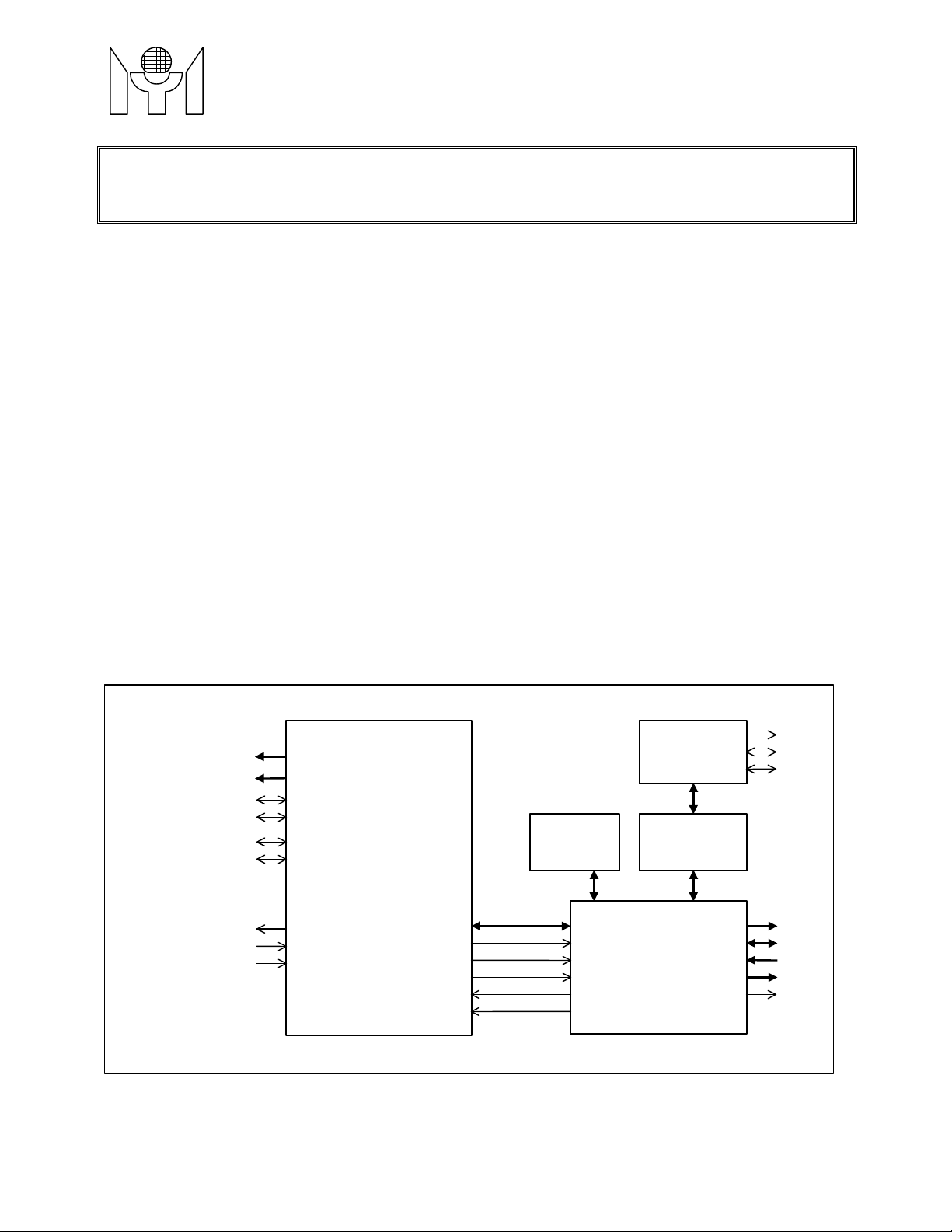
P1.0~7
8051
KSO0~7
P2.0~7
KSO8~15
P3.0
MSDATA
P3.1
MSCLK
P3.4
PS2CLK
P3.5
PS2DATA
OSC2
OSC1
RESET
DBUS
P0.0~7
/RD
/WR
ALE
/INT0
/INT1
P3.7
P3.6
ALE
P3.2
P3.3
XFR
SIE
XCVR
KSO16~17
GPIO0~1
KSI0~7
LED0~2
GPO0
V33
DP
DM
WDT
MTP805
TECHNOLOGY
(Rev. 0.9)
8051 Embedded USB/PS2 Keyboard/Mouse
Controller
FEATURES
• 8051 core, 6MHz operating frequency.
• 256-byte RAM, 8K-byte program Flash-ROM.
• Compliant with Low Speed USB Spec.1.1 including 3 Endpoints: one is Control endpoint (8-byte IN & 8-
byte OUT FIFOs), the other two are Interrupt endpoints (8-byte IN FIFOs).
• Built-in 3.3V regulator for USB Interface.
• Suspend / Resume operation.
• Idle and Power down mode wake-up by interrupt.
• 8 dedicated Key scan input pins and 18/19 Key scan output pins.
• Built-in low power reset circuit and Watchdog timer.
• PS2 compatible mouse interface.
• PS2 compatible keyboard interface share with USB interface.
• CPU clock can be double by S/W setting.
• 40-pin DIP, 42-pin SDIP or 44-pin PLCC package.
GENERAL DESCRIPTIONS
The MTP805 micro-controller is an 8051 CPU core embedded device specia lly tailored to USB/PS2
Keyboard/Mouse applications. It includes an 8051 CPU core, 256-byte SRAM, Low Speed USB Interface
and an 8K-byte internal program Flash-ROM.
BL OCK DIAGRAM
This datasheet contains new product information. Myson Technology reserv es the rights to modify the product specification without
notice. No liability is assumed as a result of the use of this product. No rights under any patent accompany the sale of the product.
Revision 0.9 - 1 - 2000/07/19

MYSON
VSS
KSI0
KSI1
KSI2
KSI3
KSI4
KSI5
KSI6
KSI7
KSO1024KSO11
KSO12
KSO9
KSO13
KSO14
NC
KSO5
KSO6
KSO7
KSO8
23222120282726
25
KSI1
6543214443424140
KSI0
RST
OSC2
OSC1
VSS
DP/PS2CLK
DM/PS2DATA
V33
VDD
NC
19
18
VSS
KSI0
KSI1
KSI2
KSI3
KSI4
KSI5
KSI6
KSI7
VSS
KSI0
KSI1
KSI2
KSI3
KSI4
KSI5
KSI6
KSI7
MTP805
TECHNOLOGY
PIN CONNECTION
RST
2
3
4
5
6
7
8
9
10
11
12
13
14
15
16
17
18
19
20
MTP805
40 Pin
PDIP #1
OSC1
OSC2
KSO0
KSO1
KSO2
KSO3
KSO4
KSO5
KSO6
KSO7
401
DP/PS2CLK
39
DM/PS2DATA
38
V33
37
VDD
36
LED0
35
LED1
34
LED2
33
MSCLK
32
MSDATA
31
GPIO0
30
KSO17
29
KSO16
28
KSO15
27
KSO14
26
KSO13
25
KSO12
24
KSO11
23
KSO10
22
KSO9
21
KSO8
(Rev. 0.9)
401
OSC1
OSC2
RST
KSO0
KSO1
KSO2
KSO3
KSO4
KSO5
KSO6
KSO7
2
3
4
5
6
7
8
9
10
11
12
13
14
15
16
17
18
19
20
MTP805
40 Pin
PDIP #2
39
38
37
36
35
34
33
32
31
30
29
28
27
26
25
24
23
22
21
DP/PS2CLK
DM/PS2DATA
V33
VDD
LED0
LED1
LED2
GPO0
MSCLK
MSDATA
KSO17
KSO16
KSO15
KSO14
KSO13
KSO12
KSO11
KSO10
KSO9
KSO8
OSC1
OSC2
RST
KSO0
KSO1
KSO2
KSO3
KSO4
KSO5
KSO6
KSO7
KSO8
1
2
3
4
5
6
7
8
9
10
11
12
13
14
15
16
17
18
19
20
MTP805
42 Pin
SDIP
DP/PS2CLK
42
DM/PS2DATA
41
40
V33
39
VDD
38
LED0
37
LED1
36
LED2
35
GPO0
34
MSCLK
33
MSDATA
32
GPIO1
31
GPIO0
30
KSO17
29
KSO16
28
KSO15
27
KSO14
26
KSO13
25
KSO12
24
KSO11
23
KSO10
2221
KSO9
KSI2
KSI3
KSI4
KSI5
KSI6
KSI7
KSO0
KSO1
KSO2
KSO3
KSO4
7
8
9
10
11
12
13
14
15
16
17
MTP805
44 Pin
PLCC
39
38
37
36
35
34
33
32
31
30
29
LED0
LED1
LED2
GPO0
MSCLK
MSDATA
GPIO1
GPIO0
KSO17
KSO16
KSO15
Revision 0.9 - 2 - 2000/07/19

MYSON
DM/PS2DATA
MTP805
TECHNOLOGY
PIN DESCRIPTION
Name Type Description
VSS
OSC1
OSC2
RST
KSI0
KSI1
KSI2
KSI3
KSI4
KSI5
KSI6
KSI7
KSO0
KSO1
KSO2
KSO3
KSO4
KSO5
KSO6
KSO7
KSO8
KSO9
KSO10
KSO11
KSO12
KSO13
KSO14
KSO15
KSO16
KSO17
GPIO0
GPIO1
MSDATA
MSCLK
GPO0
LED2
LED1
LED0
VDD
V33
DP/PS2CLK
- Ground.
I Oscillator input.
O Oscillator output.
I Active high reset. (with internal pull-down resistor)
I Key scan input 0. (Schmitt-trigger with 10K/33K/50K pull-up resistor)
I Key scan input 1. (Schmitt-trigger with 10K/33K/50K pull-up resistor)
I Key scan input 2. (Schmitt-trigger with 10K/33K/50K pull-up resistor)
I Key scan input 3. (Schmitt-trigger with 10K/33K/50K pull-up resistor)
I Key scan input 4. (Schmitt-trigger with 10K/33K/50K pull-up resistor)
I Key scan input 5. (Schmitt-trigger with 10K/33K/50K pull-up resistor)
I Key scan input 6. (Schmitt-trigger with 10K/33K/50K pull-up resistor)
I Key scan input 7. (Schmitt-trigger with 10K/33K/50K pull-up resistor)
O Key scan output 0 (8051’s P1.0). (Pseudo open-drain)
O Key scan output 1 (8051’s P1.1). (Pseudo open-drain)
O Key scan output 2 (8051’s P1.2). (Pseudo open-drain)
O Key scan output 3 (8051’s P1.3). (Pseudo open-drain)
O Key scan output 4 (8051’s P1.4). (Pseudo open-drain)
O Key scan output 5 (8051’s P1.5). (Pseudo open-drain)
O Key scan output 6 (8051’s P1.6). (Pseudo open-drain)
O Key scan output 7 (8051’s P1.7). (Pseudo open-drain)
O Key scan output 8 (8051’s P2.0). (Pseudo open-drain)
O Key scan output 9 (8051’s P2.1). (Pseudo open-drain)
O Key scan output 10 (8051’s P2.2). (Pseudo open-drain)
O Key scan output 11 (8051’s P2.3). (Pseudo open-drain)
O Key scan output 12 (8051’s P2.4). (Pseudo open-drain)
O Key scan output 13 (8051’s P2.5). (Pseudo open-drain)
O Key scan output 14 (8051’s P2.6). (Pseudo open-drain)
O Key scan output 15 (8051’s P2.7). (Pseudo open-drain)
I/O Key scan output 16. (Pseudo open-drain)
I/O Key scan output 17. (Pseudo open-drain)
I/O General purpose I/O 0. (Pseudo open-drain)
I/O General purpose I/O 1. (Pseudo open-drain)
I/O Mouse data (8051’s P3.0). (Pseudo open-drain)
I/O Mouse clock (8051’s P3.1). (Pseudo open-drain)
O General purpose output 0. (Open-drain with 420 ohm serial resistor)
O Output pin to drive LED 2. (Open-drain with 420 ohm serial resistor)
O Output pin to drive LED 1. (Open-drain with 420 ohm serial resistor)
O Output pin to drive LED 0. (Open-drain with 420 ohm serial resistor)
- Positive Power Supply.
O 3.3 Volt USB regulator output. (Must connect to 1uF or larger capacitor)
I/O USB DM / PS2 keyboard data (8051’s P3.5).
I/O USB DP / PS2 keyboard clock (8051’s P3.4).
(Rev. 0.9)
“Pseudo open-drain” pin is 8051 Port1’s standard. It can sink at least 4mA current when output low level, and
drive at least 4mA current for 2 X’tal cycle when output transit from low to high, then keep drive 100uA to
maintain the pin at high level.
Revision 0.9 - 3 - 2000/07/19

MYSON
MTP805
TECHNOLOGY
(Rev. 0.9)
FUNCTIONAL DESCRIPTIONS
1. 8051 CPU Core
MTP805 includes all 8051 functions with the following exceptions:
1.1 PSEN, ALE, #RD and #WR pins are disabled. The external RAM access is restricted to XFRs within the
MTP805.
1.2 Port0, port3.2, port3.3, port3.6 and port3.7 are not general-purpose I/O ports. They are dedicated to
special application.
1.3 #INT0 and #INT1 input pin is not provided, it is connected to special interrupt sources.
1.4 UART and Timer1 are not supported.
Note: All registers listed in this document reside in external RAM area (XFR). For internal RAM memory map
please refer to 8051 spec.
2. Memory Allo cati on
2.1 Internal Special Function Registers (SFR)
The SFR is a group of registers that are the same as standard 8051.
2.2 Internal RAM
There are total 256 bytes internal RAM in MTP805, same as standard 8052.
2.3 External Special Function Registers (XFR)
The XFR is a group of registers allocated in the 8051 external RAM area 00h - 2Fh. Most of the registers are
used for USB function. Program can initialize Ri value and use "MOVX" instruction to access these registers.
FFh
Internal RAM
Accessible by
addressing only
MOV A,@Ri
instruction)
80h
7Fh
Internal RAM
Accessible by
direct and indirect
addressing
00h
indirect
(Using
SFR
Accessible by
direct addressing
2Fh
Accessible by
indirect external
RAM addressing
MOVX A,@Ri
00h
XFR
(Using
instruction
Revision 0.9 - 4 - 2000/07/19

MYSON
MTP805
TECHNOLOGY
(Rev. 0.9)
3. I/O Pin Usage
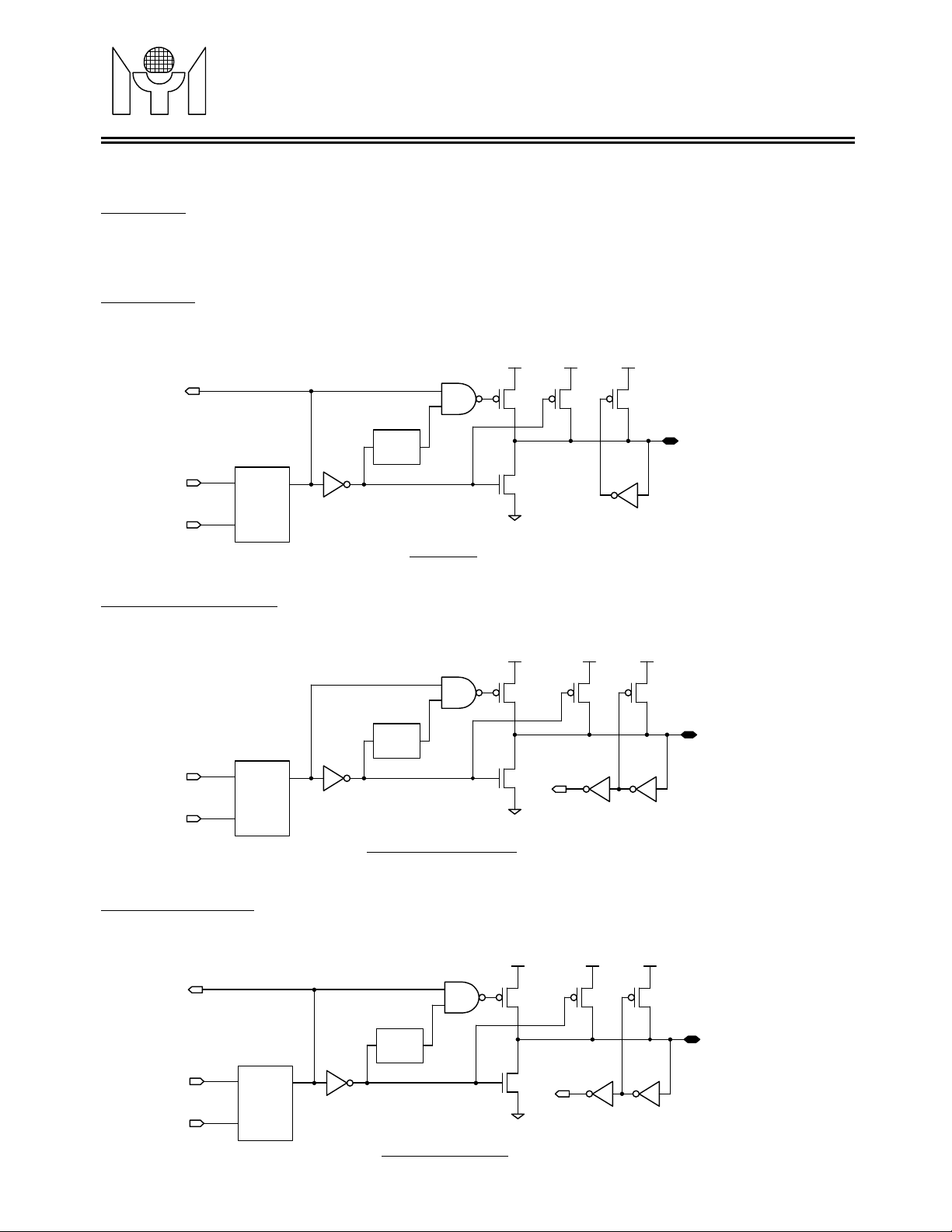
3.1 KSO0~7
These pins are direct output from the 8051’s Port1 and dedicated for key scan output. The pin’s input
function is removed. Read 8051’s Port1 is only read the data in the Port1’s output register. These pins are
“Pseudo open-drain” structure.
3.2 KSO8~15
These pins are direct output from the 8051’s Port2 and dedicated for key scan output. The pin’s input
function is removed. Read 8051’s Port2 is only read the data in the Port2’s output register. These pins are
“Pseudo open-drain” structure.
Read
Data
Write
Data
/WR
Output
Register
CK
4mA 50uA
2 OSC
period
delay
QD
4mA
500uA
Pin
KSO0~15
3.3 KSO16~17, GPIO0~1
These pins are output from MTP805’s XFR. They can be used as key scan output or general purpose I/O.
Read these pins will read the data on pin. These pins are also “Pseudo open-drain” structure.
Write
Data
/WR
Output
Register
CK
4mA 50uA
1 OSC
period
delay
QD
4mA
Read
Data
500uA
Pin
KSO16~17, GPIO0~1
3.4 MSCLK, MSDATA
These pins are connected to 8051’s P3.1 and P3.0. The usage of these pins are the same as standard 8051
except the UART’s function being not provided. These pins are also “Pseudo open-drain” structure.
Read
Latch
Data
Write
Data
/WR
Output
Register
CK
4mA 50uA
2 OSC
period
delay
QD
4mA
Read
Pin
Data
500uA
Pin
MSCLK, MSDATA
Revision 0.9 - 5 - 2000/07/19
 Loading...