MXIC MX98L715BEC Datasheet

1. FEATURES10/100M
PRELIMINARY
MX98L715BEC
3.3V SINGLE CHIP FAST ETHERNET NIC CONTROLLER
Ethernet Interface
• A single chip solution integrates 100/10 Base-T fast
Ethernet MAC, PHY and PMD
• Fully comply to IEEE 802.3u specification
• Operates over 100 meters of STP and cat 5 UTP cable
• Support full and half duplex operations in both 100
Base-TX and 10 Base-T mode
• Supports IEEE802.3x Frame Based Flow Control
scheme in full duplex mode.
• Supports transmission and reception of IEEE802.1Q
tagged frames.
• Supports QoS with prioritized traffic.
• Supports network and communication device class
OnNow requirements for Microsoft's PC99 specifications, including 3 wake up events :
- Link Change (link-on)
- Wake Up Frames
- Magic Packet
• 100/10 Base-T NWAY auto-negotiation function
• Support up to 5 LEDs for various network activities
• Supports early interrupt on both transmit and receive
operations.
• Support a variety of flexible address filtering modes
with 16 CAM address and 64 bits hash table
Home PNA interface
• Support 7-wire general purpose serial interface to link
with 1M8 PHY for home networking
PCI/MiniPCI interface
• Fully comply to PCI spec. 2.2 and Mini PCI spec. 0.73
up to 33MHz
• Fully comply to Advanced Configuration and Power
Interface (ACPI) Rev 1.1
• Fully comply to PCI Bus Power Management Interface
spec. Rev 1.1
• Bus master architecture with linked host buffers delivers the most optimized performance
• 32-bit bus master DMA channel provides ultra low
CPU utilization suitable for server and windows applications.
• Proprietary Adaptive Network Throughput Control
(ANTC) technology to optimize data integrity and
throughput
Other features
• Large on-chip FIFOs for both transmit and receive
operations without external local memory
• Support up to 128K bytes boot ROM/Flash interface
• MicroWire interface to EEPROM for customer's IDs
and configuration data
• Single 3.3V power supply, CMOS technology, 128-pin
PQFP package
( Magic Packet Technology is a trademark of Advanced Micro Device Corp. )
2. GENERAL DESCRIPTIONS
The MX98L715BEC controller is an IEEE802.3u compliant single chip 32-bit full duplex, 10/100Mbps highly
integrated Fast Ethernet combo solution, designed to
address high performance local area networking (LAN)
system application requirements.
MX98L715BEC's PCI bus master architecture delivers
the optimized performance for future high speed and powerful processor technologies. In other words, the
MX98L715BEC not only keeps CPU utilization low while
maximizing data throughput, but it also optimizes the
PCI bandwidth providing the highest PCI bandwidth utilization. To further reduce maintenance costs the
MX98L715BEC uses drivers that are backward compatible with the original MXIC MX98715 series controllers.
P/N:PM0695 REV. 0.3, MAR. 30, 2001
The MX98L715BEC contains a PCI local bus glueless
interface, a Direct Memory Access (DMA) buffer management unit, an IEEE802.3u-compliant Media Access
Controller (MAC), large T ransmit and Receive FIFOs , and
an on-chip 10 Base-T and 100 Base-TX transceiver simplifying system design and improving high speed signal
quality. Full-duplex operation are supported in both 10
Base-T and 100 Base-TX modes that increases the
controller's operating bandwidth up to 200Mbps.
Equipped with intelligent IEEE802.3u-compliant auto-negotiation, the MX98L715BEC-based adapter allows a
single RJ-45 connector to link with the other IEEE802.3ucompliant device without re-configuration.
1

In MX98L715BEC, an innovative and proprietary design
"Adaptive Network Throughput Control" (ANTC) is builtin to configure itself automatically by MXIC's driver based
on the PCI burst throughput of different PCs . With this
proprietary design, MX98L715BEC can always optimize
its operating bandwidth, network data integrity and
throughput for different PCs.
The MX98L715BEC features Remote-P ower-On and Remote-Wake-Up capability and is compliant with the Advanced Configuration and Power Interface version 1.0
(ACPI). This support enables a wide range of wak e-up
capabilities, including the ability to customize the content of specified packet which PC should respond to,
even when it is in a low-power state. PCs and workstations could take advantage of these capabilities of being waked up and served simultaneous over the network
by remote server or workstation. It helps organizations
reduce their maintenance cost of PC network.
The 32-bit multiplexed bus interface unit of
MX98L715BEC provides a direct interface to a PCI local bus, simplifying the design of an Ethernet adapter in
a PC system. With its on-chip support for both little and
big ending byte alignment, MX98L715BEC can also address non-PC applications.
MX98L715BEC
P/N:PM0695
REV. 0.3, MAR. 30, 2001
2
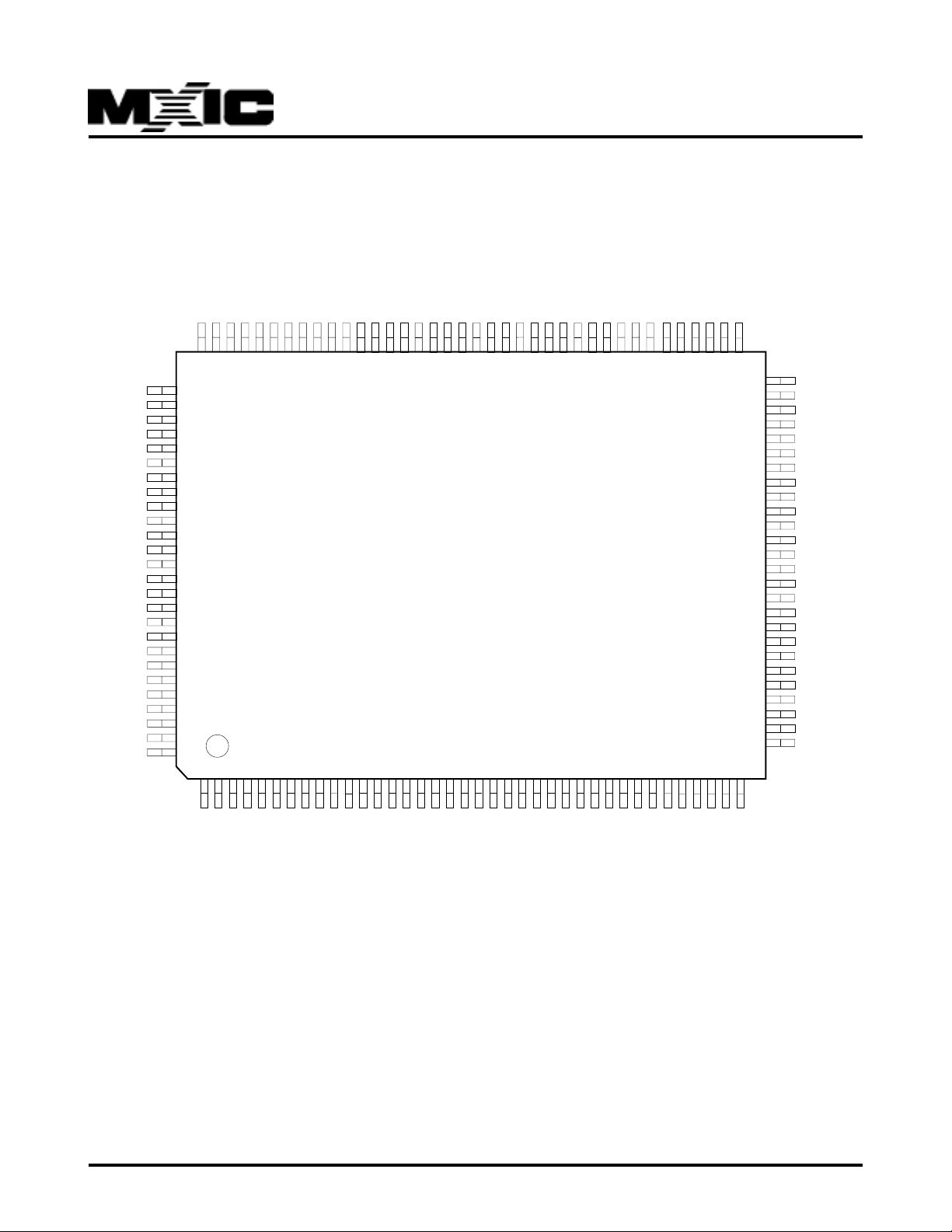
3. PIN CONFIGURATIONS
RTX
GNDA
GNDA
TXOP
TXON
VDDA
9998979695949392919089888786858483828180797877767574737271706968676665
102
101
100
VDDA
GNDA
VDDR
GNDR
CLKRUNB
ISOLATE
LANWAKE
PMEB
INTAB
RSTB
PCICLK
GNTB
REQB
AD31
AD30
GND
AD29
AD28
VDD
AD27
GND
AD26
AD25
GND
AD24
CBEB3
103
104
105
106
107
108
109
110
111
112
113
114
115
116
117
118
119
120
121
122
123
124
125
126
127
128
12345678910111213141516171819202122232425262728293031323334353637
GNDA
GNDR
VDDR
RXIP
RXIN
VDDR
GNDR
VDDA
GNDAXOXI/CKREF
VDDA
GNDA
MX98L715BEC
GNDA
VDDA
(LED3)FOEB
(LED2)BPA16
(LED1)BPA15
(LED0)BPA14
MX98L715BEC
(LED4)BPA13
GND
VDD
BPA12
BPA11
BPA10
BPA9
FCSB(VAUX)
FWEB(HLINKB)
BPA8
BPA7
BPA6
BPA5
64
63
62
61
60
59
58
57
56
55
54
53
52
51
50
49
48
47
46
45
44
43
42
41
40
39
38
BPA4
BPA3
BPA2
BPA1(EEDI)
BPA0(EECK)
EECS
BPD0(EED0)
BPD1(TXE)
BPD2(TXD)
BPD3(RXD)
BPD4(RXC)
BPD5(COL)
BPD6(CRS)
BPD7(TXC)
GND
VDD
AD0
AD1
GND
AD2
AD3
VDD
AD4
AD5
GND
AD6
P/N:PM0695
GND
IDSEL
AD23
AD22
GND
AD21
AD20
VDD
AD19
AD18
GND
AD17
AD16
CBEB2
FRAMEB
GND
IRDYB
TRDYB
DEVSELB
STOPB
VDD
PERRB
SERRB
PAR
AD15
CBEB1
GND
AD14
AD13
VDD
AD12
AD11
AD10
GND
AD9
AD8
AD7
CBEB0
REV. 0.3, MAR. 30, 2001
3

MX98L715BEC
4. PIN DESCRIPTION ( 128 PIN PQFP )
( T/S : tri-state, S/T/S : sustained tri-state, I : input, O : output, O/D : open drain )
Pin Name Type Pin No 128 Pin Function and Driver
AD[31:0] T/S 116, 117 PCI address/data bus: shared PCI address/data bus lines. Little or big ending
119,120, byte ordering are supported.
122,124,
125,127,
3,4,6,7,9,
10,12,13,
26,28,29,
31-33,35,
36,38,39,
41,42,44,
45,47,48
CBEB[3:0] T/S 128,14 PCI command and byte enable bus: shared PCI command byte enable bus,
25,37 during the address phase of the transaction, these four bits provide the bus
command. During the data phase, these four bits provide the byte enable.
FRAMEB S/T/S 1 5 PCI FRAMEB signal: shared PCI cycle start signal, asserted to indicate the
beginning of a bus transaction. As long as FRAMEB is asserted, data
transfers continue.
TRDYB S/T/S 1 8 PCI Target ready: issued by the target agent, a data phase is completed on
the rising edge of PCICLK when both IRD YB and TRDYB are asserted.
IRDYB S/T/S 1 7 PCI Master ready: indicates the bus master's ability to complete the current
data phase of the transaction. A data phase is completed on any rising edge
of PCICLK when both IRD YB and TRD YB are asserted.
DEVSELB S/T/S 19 PCI slave device select: asserted by the target of the current bus access.
When MX98L715BEC is the initiator of current bus access, the target must
assert DEVSELB within 5 bus cycles, otherwise cycle is aborted.
IDSEL I 1 PCI initialization device select: target specific device select signal for
configuration cycles issued by host.
PCICLK I 113 PCI bus clock input: PCI bus clock range from 16MHz to 33MHz.
RSTB I 112 PCI bus reset: host system hardware reset.
LANWAKE O 109 LAN wake up signal:asserts high to indicate one of the 3 wake up ev ents has
been detested in remote power on mode.
INTAB O /D 111 PCI bus interrupt request signal: wired to INTAB line.
SERRB O/ D 23 PCI bus system error signal: If an address parity error is detected and CFCS
bit 8 is enabled, SERRB and CFCS's bit 30 will be asserted.
PERRB S/T/S 22 PCI bus data error signal: As a b us master , when a data parity error is
detected and CFCS bit 8 is enabled, CFCS bit 24 and CSR5 bit 13 will be
asserted. As a bus target, a data parity error will cause PERRB to be
asserted.
P/N:PM0695
REV. 0.3, MAR. 30, 2001
4

MX98L715BEC
Pin Name Type Pin No 128 Pin Function and Driver
PAR T/S 2 4 PCI bus parity bit: shared PCI bus even parity bit for 32 bits AD bus and CBE
bus.
ST OP B S/T/S 20 PCI Target requested transf er stop signal: as b us master, assertion of STOPB
cause MX98L715BEC either to retry , disconnect, or abort.
REQB T/S 115 PCI bus request signal: to initiate a bus master cycle request
GNTB I 114 PCI bus grant acknowledge signal: host asserts to inform MX98L715BEC
that access to the bus is granted
EECS O 59 EEPROM Chip Select pin.
BPA1 O 61 Boot PROM address bit 1(EECS=0): together with BPA[15:0] to access
(EEDI) external boot PROM up to 256KB.
EEPROM data in(EECS=1): EEPROM serial data input pin.
BPA0 O 6 0 Boot PROM address bit 0(EECS=0): together with BPA[15:0] to access
(EECK) external boot PROM up to 256KB.
EEPROM clock(EECS=1): EEPROM clock input pin
BPA[12:0] O 74-71, Boot PROM address line.
68-60
BPA13 O 77 Boot PROM address line 13 ( LED4 )
(LED4)
BPA14 O 78 Boot PROM address line 14 (LED0)
( LED0)
BPA15 O 79 Boot PROM address line 15 ( LED1)
( LED1)
BPA16 O 80 Boot PROM address line 16 ( LED2)
( LED2)
BPD0 T/S 58 Boot PROM data line 0(EECS=0): boot PROM or flash data line 0.
(EEDO) EEPROM data out(EECS=1): EEPROM serial data outpin(during reset
initialization).
BPD[7:0] T/S 51-58 Boot PROM data lines: boot PROM or flash data lines 7-0.
FWEB T/S 69 Flash Write Enable Output ( or Home PNA Link activ e low input )
( HLINKB)
FCSB T/S 7 0 Boot PROM Chip Select Output or A uxiliary Vdd input with 10k e xternal
( V A UX) resistor pull-up. (Internal pull-down)
FOEB O 81 Boot PROM Output Enable ( LED3 )
( LED3 )
RTX O 102 Connecting an external resistor to ground, Resistor value=1K ohms
PMEB O/D 1 10 P ower Management Event Status Output
P/N:PM0695
REV. 0.3, MAR. 30, 2001
5

MX98L715BEC
Pin Name Type Pin No 128 Pin Function and Driver
RXIP I 93 Twisted pair receive differential input: Support both 10 Base-T and 100
Base-TX receive differential input.
RXIN I 92 Twisted pair receiv e differential input: Support both 10 Base-T and 100
Base-TX receive differential input
TXOP O 99 Twisted pair transmit differential output: Support both 10 Base-T and 100
Base-TX transmit differential output
TXON O 9 8 Twisted pair transmit diff erential output: Support both 10 Base-T and 100
Base-TX transmit differential output
XI/CKREF I 86 Reference clock: 25MHz oscillator clock input or Crystal in pin
XO I 8 7 Crystal out pin
LED0 O 78 Programmable LED0 pin:
CSR9.28=1 Set the LED0 as Link Speed (10/100) LED.
CSR9.28=0 Set the LED0 as Activity LED.
Default is Activity LED after reset.
LED1 O 79 Programmable LED1 pin:
CSR9.29=1 Set the LED1 as Link/Activity LED.
CSR9.29=0 Set the LED1 as Good Link LED.
Default is Good Link LED after reset.
LED2 O 80 Programmable LED2 pin:
CSR9.30=1 Set the LED2 as Collision LED .
CSR9.30=0 Set the LED2 as Link Speed (10/100) LED.
Default is Link Speed (10/100) LED after reset.
LED3 O 81 Programmable LED3 pin:
CSR9.31=1 Set the LED3 as Full/Half Duplex LED .
CSR9.31=0 Set the LED3 as RX LED.
Default is RX LED after reset.
LED4 O 77 Programmable LED4 pin:
CSR9.24=1 Set the LED4 as Pow er Management Event LED .
CSR9.24=0 Set the LED4 as COL LED.
Default is Collision LED after reset.
VDD P 8,21,30,43, Digital Power pins.
49,75,121
GN D G 2,5,11,16,27 Digital Ground pins.
34,40,46,50
76,118,123,
126
P/N:PM0695
REV. 0.3, MAR. 30, 2001
6

MX98L715BEC
Pin Name Type Pin No 128 Pin Function and Driver
VDDA P 82, 85, 89, Analog P ow er pins.
97,103,
GN D A G 83,84,88,96, Analog Ground pins.
100,101,104,
VDDR P 91, 94,105 Receive Channel Po wer pins.
GNDR G 90, 95,106 Receive Channel Ground pins.
TXE T/S 57 Transmit Enable Output : TXE signal in 7 wire interface for Home PNA
( BPD1) connection. ( Or BPD1 pin during Flash or boot ROM activities )
TXD T/S 56 Transmit Data Output : TXD signal in 7 wire interf ace f or Home PNA
( BPD2) connection. ( Or BPD2 pin during Flash or boot ROM activities )
RX D T/S 55 Receive Data Input : RXD signal in 7 wire interface for Home PNA
( BPD3) connection. ( Or BPD3 pin during Flash or boot ROM activities )
RX C T/S 54 Receive Clock Input : RXC signal in 7 wire interface for Home PNA
( BPD4) connection. ( Or BPD4 pin during Flash or boot ROM activities )
COL T/S 53 Collision Input : COL signal in 7 wire interface for Home PNA
( BPD5) connection. ( Or BPD5 pin during Flash or boot ROM activities )
CR S T/S 52 Transmit Enable Output : CRS signal in 7 wire interf ace f or Home PNA
( BPD6) connection. ( Or BPD6 pin during Flash or boot ROM activities )
TXC T/S 51 Transmit Clock Input : TXC signal in 7 wire interface for Home PNA
( BPD7) connection. ( Or BPD7 pin during Flash or boot ROM activities )
CLKRUNB T/S 107 Mini PCI bus CLock Run pin : Indicates the MiniPCI clock status, normally
controlled by host, low for normal clocking, high when clock is about to be
slowed down. Can be asserted low by MX98L715BEC to request normal
clocking when necessary .
ISOLATE T/S 10 8 ISOLATE pin : Output pin to isolate e xternal Home PNA PHY chip
P/N:PM0695
REV. 0.3, MAR. 30, 2001
7
5. PROGRAMMING INTERFACE
5.1 PCI CONFIGURA TION REGISTERS:
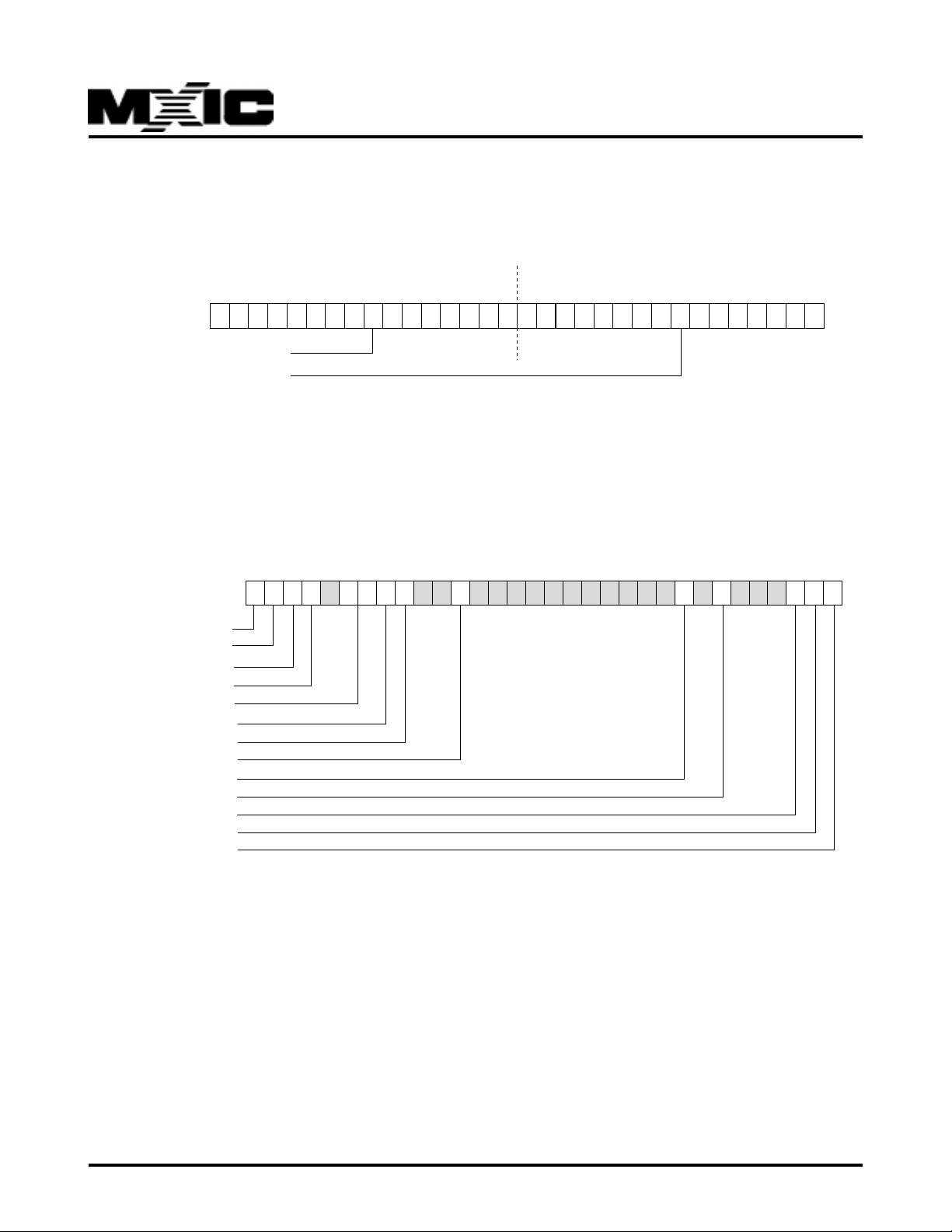
5.1.1 PCI ID REGISTER ( PFID ) ( Offset 03h-00h )
MX98L715BEC
31 30 29 28 27 26 25 24 23 22 21 20 19 18 17 16
Device ID (bit 31:16)
Vendor ID (bit 15:0)
15 14 13 12 11 10 9 8 7 6 5 4 3 2 1 0
This register can be loaded from external serial EEPROM or use a MXIC preset value of "10D9" and "0531" for vendor
ID and device ID respectively. Word location 3Eh and 3Dh in serial EEPROM are used to configure customer's
vendor ID and device ID respectiv ely . If location 3Eh contains"FFFF" value then MXIC's v endor ID and device ID will
be set in this register, otherwise both 3Eh and 3Dh will be loaded into this register from serial EEPROM.
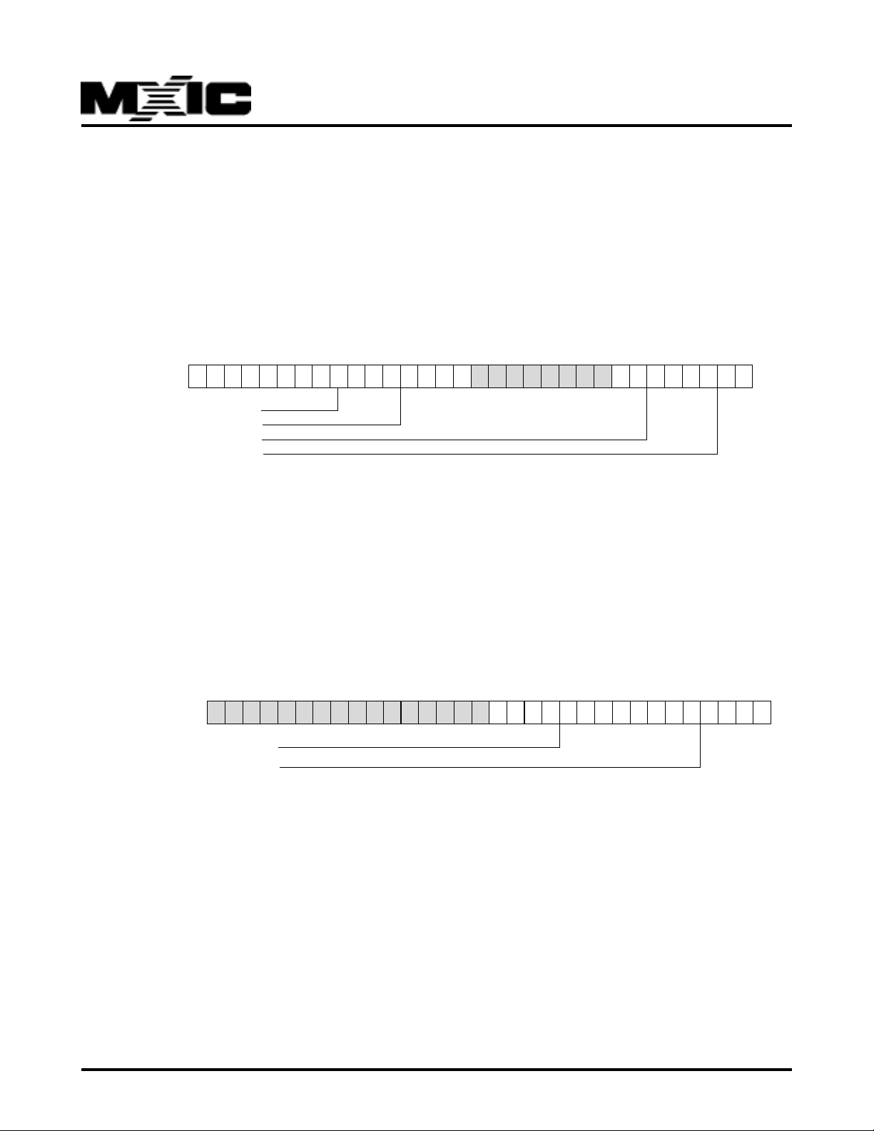
5.1.2 PCI COMMAND AND ST A TUS REGISTER ( PFCS ) ( Offset 07h-04h )
31 30 29 28 27 26 25 24 23 22 21 20 19 18 17 16
Detect Parity Error
Signal System Error
Receive Master Abort
Receive Target Abort
Deceive Select Timing
Data Parity Report
Fast Back-to-back
New Capability
System Error Enable
Parity Error Response
Master Operation
Memory Space Access
IO Space Access
15 14 13 12 11 10 9 8 7 6 5 4 3 2 1 0
The bit content will be reset to 0 when a 1 is written to the corresponding bit location.
bit 0 : IO Space Access, set to 1 enable IO access
bit 1 : Memory Space Access, set to 1 to enable memory access
bit 2 : Master Oper ation, set to 1 to support bus master mode
bit 5-3 : not used
bit 6 : P arity Error Response, set to 1 to enab le assertion of CSR<13> bit if parity error detected.
bit 7 : not used
bit 8 : System Error Enable, set to 1 to enable SERR# when parity error is detected on address lines and CBE[3:0].
bit 20 : Ne w capability. Set to support PCI power management.
bit 22-bit19 : not used
bit 23 : Fast Back-to back, always set to accept fast back-to-back transactions that are not sent to the same bus
device.
P/N:PM0695
8
REV. 0.3, MAR. 30, 2001
MX98L715BEC
bit 24:Data Parity Report, is set to 1 only if PERR# active and PFCS<6> is also set.
bit 26-25:Device Select Timing of DEVSELB pin.
bit 27:not used
bit 28:Receive Target Abort, is set to indicate a transaction is terminated by a target abort.
bit 29:Receive Master Abort, is set to indicate a master transaction with Master abort.
bit 30:Signal System Error, is set to indicate assertion of SERRB.
bit 31:Detected Parity Error , is set whenev er a parity error detected regardless of PFCS<6>.
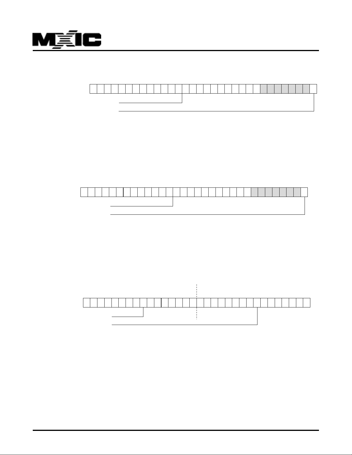
5.1.3 PCI REVISION REGISTER ( PFRV ) ( Offset 0Bh-08h )
31 30 29 28 27 26 25 24 23 22 21 20 19 18 17 16
Base Class
Subclass
Revision Number
Step Number
15 14 13 12 11 10 9 8 7 6 5 4 3 2 1 0
bit 3 - 0 : Step Number, range from 0 to Fh.
bit 7 - 4 : Re vision Number , fix ed to 6h f or MX98L715BEC
bit 15 - 8 : not used
bit 23 - 16 : Subclass, fixed to 0h.
bit 31 - 24 : Base Class, fixed to 2h.
5.1.4 PCI LA TENCY TIMER REGISTER ( PFLT ) (Offset 0Fh-0Ch)
PFL T Register (0Fh-0Ch)
31 30 29 28 27 26 25 24 23 22 21 20 19 18 17 16
Configuration Latency Timer
System cache line size
15 14 13 12 11 10 9 8 7 6 5 4 3 2 1 0
bit 0 - bit 7 : System cache line size in units of 32 bit word, device driver should use this value to program CSR0<15:14>.
bit 8 - bit 15 : Configuration Latency Timer, when MX98L715BEC asser t FRAMEB, it enables its latency timer to
count.
If MX98L715BEC desserts FRAMEB prior to timer expiration, then timer is ignored. Otherwise, after timer expires,
MX98L715BEC initiates transaction termination as soon as its GNTB is deserted.
P/N:PM0695
9
REV. 0.3, MAR. 30, 2001
5.1.5 PCI BASE IO ADDRESS REGISTER ( PBIO ) ( Offset 13h-10h )
MX98L715BEC
31 30 29 28 27 26 25 24 23 22 21 20 19 18 17 16
Configuration Base Memory Address
Memory Space Indicator
15 14 13 12 11 10 9 8 7 6 5 4 3 2 1 0
bit 0 : IO/Memory Space Indicator , fixed to 1 in this field will map into the IO space. This is a read only field.
bit 7 - 1 : not used, all 0 when read
bit 31 - 8 : Defines the address assignment mapping of MX98L715BEC CSR registers.
5.1.6 PCI Base Memory Address Register ( PBMA ) ( Offset 17h-14h )
31 30 29 28 27 26 25 24 23 22 21 20 19 18 17 16
Configuration Base IO Address
IO/Memory Space Indicator
15 14 13 12 11 10 9 8 7 6 5 4 3 2 1 0
bit 0 : Memory Space Indicator , fix ed to 0 in this field will map into the memory space. This is a read only field.
bit 7 - 1 : not used, all 0 when read
bit 31 - 7 : Defines the address assignment mapping of MX98L715BEC CSR registers.
5.1.7 PCI SUBSYSTEM ID REGISTER ( PSID ) ( Offset 2Fh-2Ch )
31 30 29 28 27 26 25 24 23 22 21 20 19 18 17 16
Subsystem ID (31:16)
Subsystem Vendor ID (bit 15:0)
15 14 13 12 11 10 9 8 7 6 5 4 3 2 1 0
This register is used to uniquely identify the add-on board or subsystem where the NIC controller resides. V alues in
this register are loaded directly from external serial EEPROM after system reset automatically . W ord location 36h of
EEPROM is subsystem vendor ID and location 35h is subsystem ID.
P/N:PM0695
10
REV. 0.3, MAR. 30, 2001
MX98L715BEC
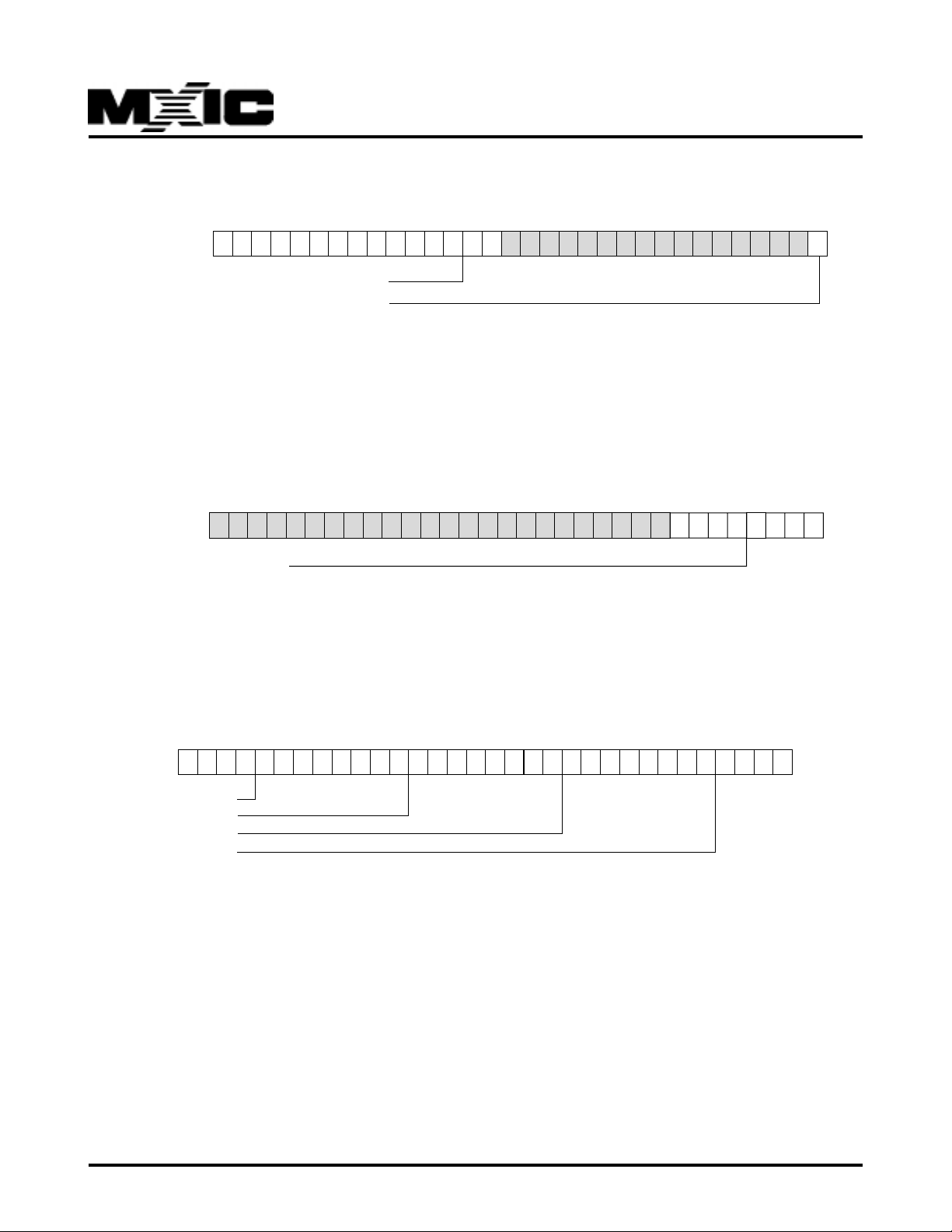
5.1.8 PCI BASE EXP ANSION R OM ADDRESS REGISTER ( PBER ) ( Offset 33h-30h )
31 30 29 28 27 26 25 24 23 22 21 20 19 18 17 16
Expansion ROM Base Address (upper 21 bit)
Address Decode Enable
15 14 13 12 11 10 9 8 7 6 5 4 3 2 1 0
bit 0 : Address Decode Enable, decoding will be enabled if only both enable bit in PFCS<1> and this expansion ROM
register are 1.
bit 16 - 1 : not use
bit 31 - 17 : Defines the upper 21 bits of expansion ROM base address.
5.1.9 PCI CAP ABILITY POINTER REGISTER ( PFCP ) ( Offset 37h-34h )
31 30 29 28 27 26 25 24 23 22 21 20 19 18 17 16
Capability Pointer (Set to 44h)
15 14 13 12 11 10 9 8 7 6 5 4 3 2 1 0
bit 7- 0 : Capability pointer (Cap_Ptr) is set to 44h.
bit 31- 8 : reserved
5.1.10 INTERRUPT REGISTER ( PFIT ) ( Offset 3Fh-3Ch )
31 30 29 28 27 26 25 24 23 22 21 20 19 18 17 16
0 0 1 1 1 0 0 0 0 0 0 0 1 0 0 0
Max_Lat
Min-Gnt
Interrupt Pin
Interrupt Line
15 14 13 12 11 10 9 8 7 6 5 4 3 2 1 0
bit 7 - 0 : Interrupt Line, system BIOS will writes the routing information into this field, driver can use this information
to determine priority and interrupt vector.
bit 15 - 8 : Interrupt Pin, fixed to 01h which use INTA#.
bit 31 - 24 : Max_Lat which is a maximum period for a access to PCI bus.
bit 23 - 16 : Min_Gnt which is the maximum period that MX98L715BEC needs to finish a burst PCI cycle.
P/N:PM0695
REV. 0.3, MAR. 30, 2001
11
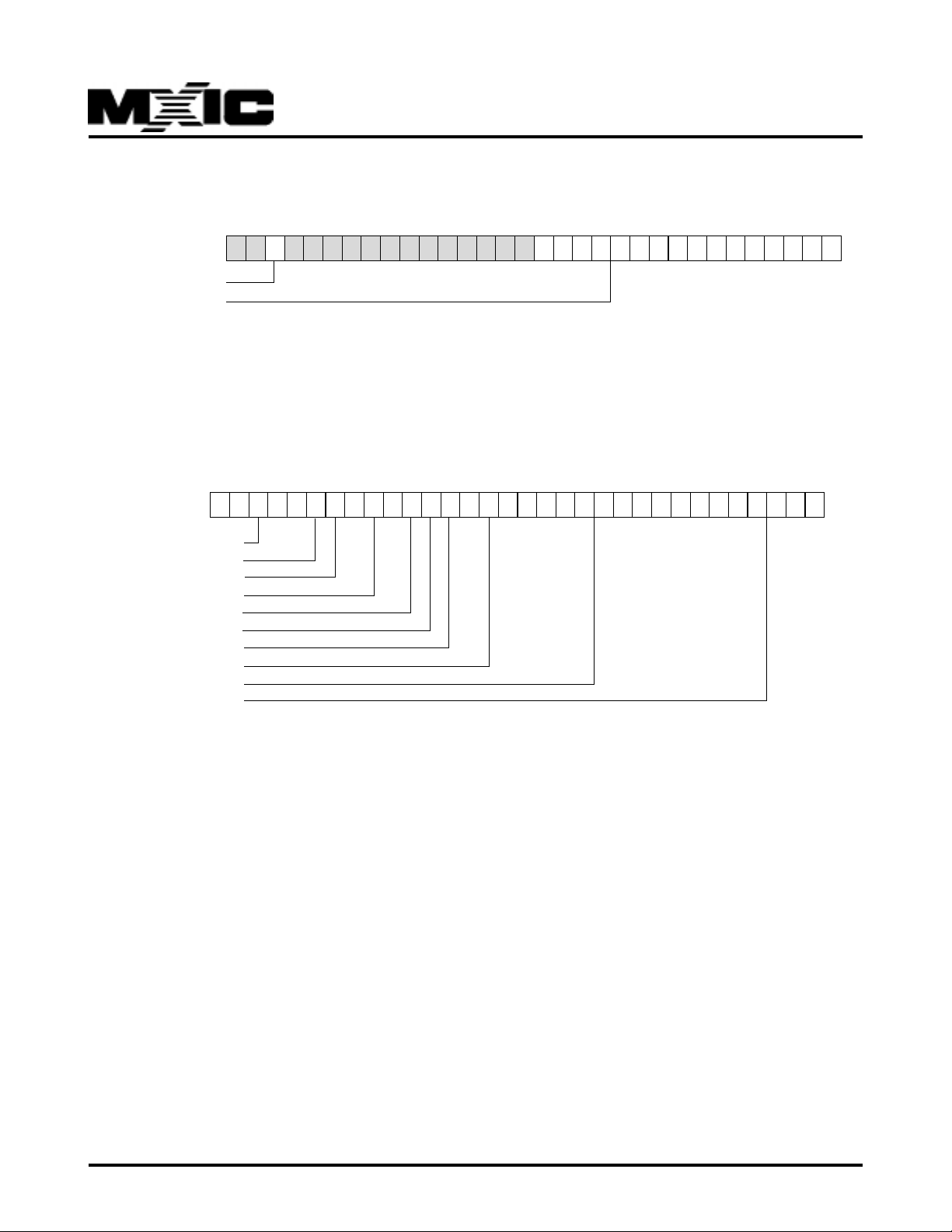
5.1.11 PCI DRIVER AREA REGISTER ( PFDA ) ( 43h-40h )
MX98L715BEC
31 30 29 28 27 26 25 24 23 22 21 20 19 18 17 16
Board T ype
Driver Special Use
15 14 13 12 11 10 9 8 7 6 5 4 3 2 1 0
bit 29 : board type
bit 15 - 8 : driver is free to read and write this field for any purpose.
bit 7 - 0 : not used.
5.1.12 PCI POWER MANA GEMENT CAP ABILITY REGISTER ( PPMC ) ( 47h-44h )
31 30 29 28 27 26 25 24 23 22 21 20 19 18 17 16
PME_Support
D2_Support
D1_Support
AUX_I
DSI
Auxiliary Power Source
PME Clock
Version
Next Pointer
Capability ID
15 14 13 12 11 10 9 8 7 6 5 4 3 2 1 0
0 0 0 0 0 0 0 0
bit 31- 27 : PME_Support, read only indicates the power states in which the function ma y assert LANW AKE pin.
bit 31 ---- PME_D3cold (value depending on V aux / FCSB pin )
bit 30 ---- PME_D3hot
bit 29 ---- PME_D2
bit 28 ---- PME_D1
bit 27 ---- PME_D0
bit 26 : D2 mode support, read only, set to 1.
bit 25 : D1 mode support, read only, set to 1.
bit 24-22 : AUX_I bits. Auxiliary current field, set to 000.
bit 21 : DSI, read only, reset to 0.
bit 20 : A uxiliary power source , supporting D3cold, set to 1. This bit is valid only when bit 15 is a '1'.
bit 19 : PME Clock, read only, reset to 0.
bit 18-16 : PCI po wer management version1.1, set to 010, read only.
bit 15-8 : Next Pointer, all bits reset to 0.
bit 7-0 : Capability ID, read only , set to 1 indicates support of power management
P/N:PM0695
12
REV. 0.3, MAR. 30, 2001

MX98L715BEC
5.1.13 PCI POWER MANA GEMENT COMMAND AND ST ATUS REGISTER ( PPMCSR ) ( 4Bh-48h )
31 30 29 28 27 26 25 24 23 22 21 20 19 18 17 16
Data
Bridge Extension Support
PME_Status
Data_Scale
Data_Select
PME_EN
Reserved
Power State
15 14 13 12 11 10 9 8 7 6 5 4 3 2 1 0
0 0 0 0 0 00 0 0 0 0 0 0 0
bit 1-0 : Power_State, read/write, D0 mode is 00, D1 mode is 01, D2 mode is 10, D3 hot mode is 11.
bit7-2 : all 0. Reserved.
bit8 : PME_EN, set 1 to enab le PMEB and LANWAKE pins. Set 0 to disable PMEB and LANWAKE assertion.
bit 12-9 : Data_Select f or report in the Data register located at bit 31:24. Not supported, reset to 0.
bit 14-13 : Data_Scale , read only, not supported, reset to 0.
bit 15 : PME_Status independent of the state of PME_EN. Cleared during power up.
When set, indicates a PME event.
Write 1 to clear the PMEB and LANWAKE assertion, PME-Status become 0. Write 0, no eff ect.
bit 21-16 : Reserved.
bit 22 : B2_B3# = 0, BPCC_EN = 1, read only, not support.
bit 23 : BPCC_EN = 0, Bus Power/Clock Control Enable, read only, not support.
bit 31-24 : Data = 0, read only, not support.
P/N:PM0695
REV. 0.3, MAR. 30, 2001
13

MX98L715BEC
5.2 HOST INTERF ACE REGISTERS
MX98L715BEC CSRs are located in the host I/O or memory address space. The CSRs are double w ord aligned and
32 bits long. Definitions and address for all CSRs are as follows :
CSR Mapping
Register Meaning Offset from CSR Base
Address ( PBIO and PBMA )
CSR0 Bus mode 0 0
CSR1 T ransmit poll demand 08 h
CSR2 Receive poll demand 10 h
CSR3 Receive list base address 18 h
CSR4 T ransmit list base address 20 h
CSR5 Interrupt status 28 h
CSR6 Operation mode 30h
CSR7 Interrupt enable 38 h
CSR8 Missed frame counter 40 h
CSR9 Serial ROM and MII management 48h
CSR10 Flash Memory Address Register 50h
CSR11 General Purpose timer 58 h
CSR12 10 Base-T status port 6 0h
CSR13 SIA Reset Register 68 h
CSR14 10 Base-T control port 7 0h
CSR15 Watchdog timer 78h
CSR16 ( Reserved ) Test Operation port 80 h
CSR17 ( Reserved ) IC Test P ort-1 88 h
CSR18 ( Reserved ) IC Test P ort-2 90 h
CSR19 ( Reserved ) IC test Port-3 98h
CSR20 Auto compensation A0h
CSR21 Flow control Register A4h
CSR22 MAC ID Byte 3-0 A8h
CSR23 Magic ID 5, 4 / MAC ID Byte 5, 4 ACh
CSR24 Magic ID Byte 3-0 B0h
CSR25 Filter 0 Byte Mask B4h
CSR26 Filter 1 Byte Mask B8h
CSR27 Filter 2 Byte Mask BCh
CSR28 Filter 3 Byte mask C0h
CRS29 Filter Offset C4h
CSR30 Filter 1&0 CRC-16 C8 h
CSR31 Filter 3&2 CRC-16 CC h
P/N:PM0695
REV. 0.3, MAR. 30, 2001
14

CSR32 Reserved A Register 1 D0 h
CSR33 Reserved A Register 2 D4 h
CSR34 Reserved A Register 3 D8 h
CSR35 Reserved A Register 4 DC h
CSR36 Reserved A Register 5 E0h
CSR37 Reserved P Register E4h
CSR38 VLAN Tag Register E8h
CSR39 Power Management Register ECh
MX98L715BEC
P/N:PM0695
REV. 0.3, MAR. 30, 2001
15
 Loading...