

MXIC MX97103FC Datasheet

FEATURE
PRELIMINARY
MX97103
ISDN S/T-PCI TRANSCEIVER
• Single chip solution for ISDN PC card with PCI interface
• Supports full duplex 2B+D ISDN S/T transceiver according to ITU I.430
• Integrate S-interface, D & B channel protocol controllers, and PCI controller
• 32-bit PCI bus interface
GENERAL DESCRIPTION
MX97103 is a single chip solution for ISDN-S connection on PCI bus. It integrates S-transceiver, D and B
channel protocol controllers, and PCI interface.
It can be divided into the following major functional bloc ks
: analog front end, la yer 1 function, GCI interface . LAPD
controller, B channel HDLC controllers, EEPR OM interface and PCI interface. The important function of each
major block will be described below.
According to ITU 1.430 spec. the S/T interface is a 4wire interface. Among them, 2 wires are used f or transmitting, and the other two are for receiving. The wiring
configurations include short passive bus, e xtended passive bus and point-to-point connection. For short passive bus , the operation distance is from 100m to 200m,
and the TEs(max 8)can be connected at random points
along the full length of the cable. F or e xtended passive
bus, TEs connect to the cable at the far end from the NT.
The total length would be at least 500m and a differential distance between TE connection points is of 25 to
50m. For point-to-point connection, the cable length can
be 1km.
• Each B channel has 2x64 byte FIFO for each direction
• D channel has 2x32 byte FIFO for each direction
• EEPROM interface for loading vendor-specific data
• One programmable LED
• Comply to ACPI Rev 1.0
• 0.5u CMOS
• 100-pin PQFP package
The layer 1 b lock comprises of PDLL, DA C, RT and MFC
functions. DPLL's function is to establish S/T frame synchronization. DAC resolves the contention issue for
differnet TE accessing D channel at the same time . R T
deals with the receiving S/T data extraction and put out
the transmitted data at the corrent time slot. MFC is the
multiframing S and Q channel control block.
GCI is the digital bus for the IC. It can accomodate 8
GCI-compatible devices . This bloc k conv erts the frame
between GCI and S/T interface.
LAPD block relieves the microprocessor of the duty to
generate HDLC frame on the D channel. It can generate flag, CRC, address and control field automatically.
And it can generate S-frame for HDLC protocol. It contains 2 FIFO of 2x32 byte each to facilitate the D pac ket
transmission and reception.
Two B channel HDLC controllers can handle tasks like
flag and CRC generation, zero insertion and deletion.
For each direction a 2x64 byte FIFO is pro vided to buffer
the data.
The analog front end deals with the signals transmitted
to and received from the wiring cable. It accepts the
digital data from layer 1 block and converts them into
appropriate signals to be sent out to the wire, and it also
receive the attenuated and distorted signal from the wire
and recover them to be processed b y la yer 1 block.
P/N:PM0564 REV. 1.0, FEB. 23, 1999
The EEPROM interface is used to load specific v endor
information after system hardware reset. V endor ID and
device ID can be load to distinguish different products.
If EEPROM is not used, default v alues will be set.
The PCI interface enables the chip attached to PCI bus
directly without any glue logic. The bus speed can be
from 25MHz to 33MHz.
1
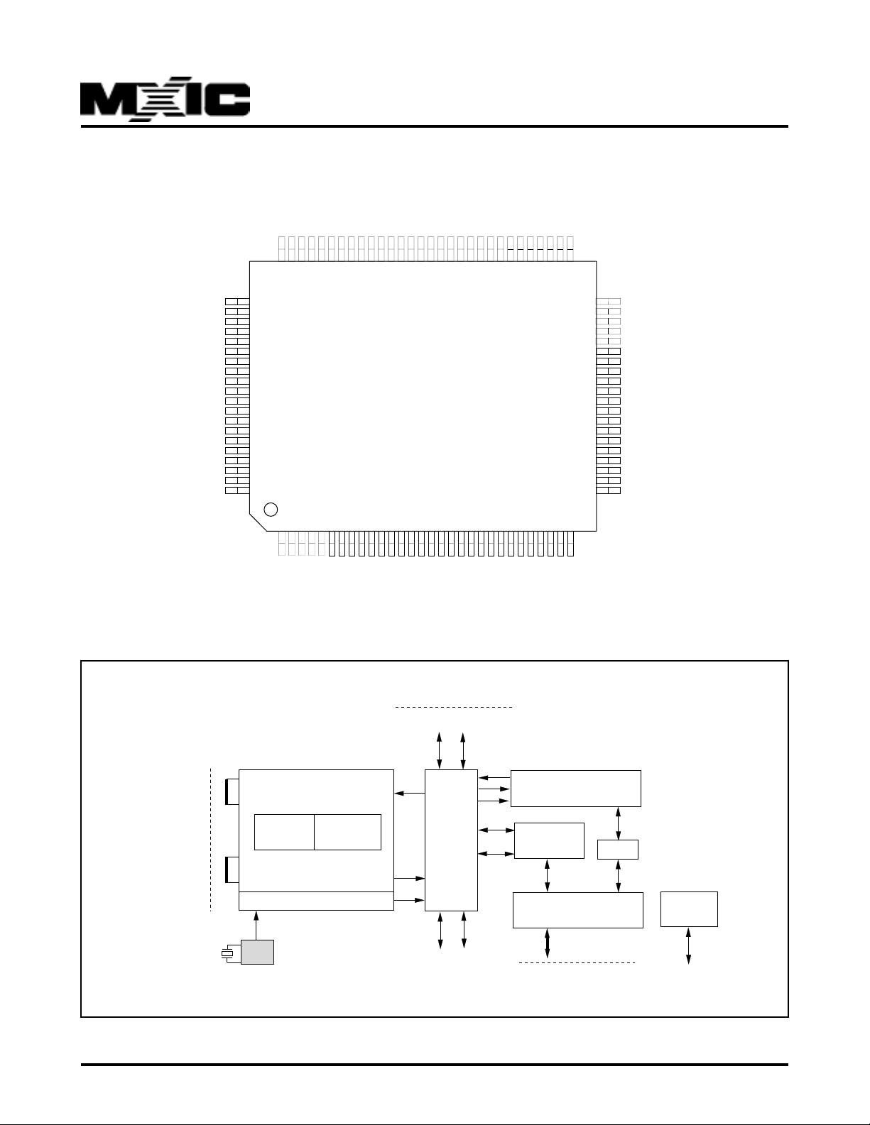
PIN CONFIGURATION
AD15
VSS
CBE1#
PAR
VDD
PERR#
STOP#
VSS
DEVSEL#
TRDY#
IRDY#
FRAME#
CBE2#
VSS
AD16
AD17
VSS
AD18
AD19
VDD
AD20
AD21
VSS
AD22
AD23
VSS
IDSEL
CBE3#
AD24
AD25
MX97103
AD14
VSS
AD13
AD12
VDD
AD11
AD10
VSS
AD9
AD8
VSS
CBE0#
AD7
AD6
VSS
AD5
AD4
VDD
AD3
AD2
BLOCK DIAGRAM
8079787776757473727170696867666564636261605958575655545352
81
82
83
84
85
86
87
88
89
90
91
92
93
94
95
96
97
98
99
100
1234567891011121314151617181920212223242526272829
AD1
AD0
VSS
VDD
EEDI
EEDO
EECK
EECS
PME
MX97103
VSS
TEST3
TEST2
LED1
TEST1
TEST4
VDD
DD
DU
FSC
DCL
VSS
SDS1
BCL
VSS
SDS2
XTAL2
XTAL1
SR2
AVSS(C)
51
30
SR1
50
49
48
47
46
45
44
43
42
41
40
39
38
37
36
35
34
33
32
31
VDD
AD26
AD17
VSS
AD28
AD29
VSS
AD30
AD31
VDD
CLK
VSS
RST#
INTA#
AVDD(C)
SX2
SX1
AVDDX
AVDD(P)
AVSS(P+X)
P/N:PM0564
S/T Interface
7.68MHZ
Transmitter
Multiframe
control
Receiver
OSC
Activation/
Deactivation
DPLL
GCI interface
DU DD
GCI
DCL FSC1
2
LAP-D&B-HDLC
B-channel
Switching FIFOS
PCI
Interface
PCI bus
EEPROM
Interface
REV. 1.0, FEB. 23, 1999
MX97103
PIN DESCRIPTION
PAD# PIN NAME TYPE DESCRIPTION
42, 43, 45, 46, 48, 49, AD[31:0] I/O PCI address/data bus.
51, 52, 56, 57, 59, 60,
62, 63, 65, 66, 80, 81,
83, 84, 86, 87, 89, 90,
93, 94, 96, 97, 99, 100,
2, 3
53, 68, 78, 92 CBE[3:0]# I PCI command/byte enable, command during address
phase, byte enable during data phase.
69 FRAME# I PCI FRAME# signal, asserted to indicate the start of a bus
transaction.
71 TRDY# O PCI Target ready, asserted by target agent.
70 IRDY# I PCI master ready, data transferred on the rising edge of
CLK when IRDY# and TRDY# both asserted.
72 DEVSEL# O PCI slave device select, specific for configuration cycle.
54 IDSEL I PCI Initialization device select, specific for configuration
cycle.
40 CLK I PCI clock, 33MHz
38 RST# I PCI bus reset
37 INTA# O/D PCI bus interrupt request
75 PERR# I/O PCI bus data error
77 PAR I/O PCI bus parity bit, even parity for AD and CBE
74 STOP# O PCI stop signal
23 BCL O GCI bit clock, 768KHz
22 SDS1 O GCI serial data strobe 1, programmable strobe signal
24 SDS2 O GCI serial data strobe 2, programmable strobe signal
19 FSC O(I) GCI frame sync
20 DCL O(I) GCI data clock, 1.536MHz
18 DU I/O GCI data upward to ST interface
17 DD I/O GCI data downward from ST interface
34 SX1 O S-bus transmitter output(positive)
35 SX2 O S-bus transmitter output(negative)
29 SR2 I S-bus receiver input
30 SR1 I S-bus receiver ref erence
27 XTAL1 I Connection f or 7.68MHz crystal/oscillator input
26 XTAL2 O Crystal output
9 LED2 O Auxillisry LED output 0
15 LED1 O Auxilliary LED output 1
P/N:PM0564
REV. 1.0, FEB. 23, 1999
3
PAD# PIN NAME TYPE DESCRIPTION
8 EECS O EEPROM chip select
7 EECK O EEPROM interf ace cloc k
6 EEDI O Output data to EEPROM
5 EEDO I Input data from EEPROM
10, 12, 13, 14 TEST[4:1] test pins
36, 33, 32 A VDD Analog po wer
31, 28 A VSS Analog ground
4, 16, 41, 50, 61, VDD Digital power
76, 85, 98
1, 11, 21, 25, 39, VSS Digital ground
44, 47, 55, 58, 64,
67, 73, 79, 82, 88,
91, 95
ABSOLUTE MAXIMUM RATINGS
MX97103
Supply Voltage(VDD) 4.75V to 5.25V
DC Input Voltage(Vin) -0.5V to VDD+0.5V
DC Output Voltage(Vout) -0.5V to VDD+0.5V
Storage T emperature Range(Tstg) -55°C to 150°C
Pow er Dissipation(PD) 500mW
Lead T emp.(TL)(Soldering, 10sec) 260°C
ESD Rating(Rzap=1.5k, Czap=100pf) 2000V
Clamp Diode Current ±20mA
P/N:PM0564
REV. 1.0, FEB. 23, 1999
4
 Loading...